Product
Folder
Order
Now
Support &
Community
Tools &
Software
Technical
Documents
LM5122ZA
SNVSB54A – MAY 2018 – REVISED NOVEMBER 2018
LM5122ZA Wide-Input Synchronous Boost Controller With Multiple Phase Capability
1 Features
2 Applications
•
•
•
•
•
•
•
•
•
•
•
•
•
•
•
•
•
•
•
•
•
•
1
•
•
•
•
Maximum Input Voltage: 65 V
Minimum Input Voltage: 3 V (4.5 V for Start-Up)
Output Voltage up to 100 V
Bypass (VOUT = VIN) Operation
1.2-V Reference with ±1% Accuracy
Free-Run and Synchronizable Switching to 1 MHz
Peak-Current-Mode Control
Robust 3-A Integrated Gate Drivers
Adaptive Dead-Time Control
Optional Diode-Emulation Mode
Programmable Cycle-by-Cycle Current Limit
Hiccup-Mode Overload Protection
Programmable Line UVLO
Programmable Soft Start
Thermal Shutdown Protection
Low Shutdown Quiescent Current: 9 μA
Programmable Slope Compensation
Programmable Skip-Cycle Mode Reduces
Standby Power
Allows External VCC Supply
Inductor DCR Current Sensing Capability
Multi-phase Capability
Thermally Enhanced 24-Pin HTSSOP
12-V, 24-V, and 48-V Power Systems
Wireless Infrastructure
Audio Power Supply
High-Current Boost Power Supply
3 Description
The LM5122ZA is a multi-phase capable
synchronous boost controller intended for highefficiency synchronous boost regulator applications.
The control method is based upon peak-current-mode
control. Current-mode control provides inherent line
feed forward, cycle-by-cycle current limiting, and ease
of loop compensation.
The switching frequency is programmable up to
1 MHz. Higher efficiency is achieved by two robust Nchannel MOSFET gate drivers with adaptive deadtime control. A user-selectable diode-emulation mode
also enables discontinuous-mode operation for
improved efficiency at light load conditions.
An internal charge pump allows 100% duty cycle for
high-side synchronous switch (bypass operation). A
180° phase shifted clock output enables easy multiphase interleaved configuration. Additional features
include thermal shutdown, frequency synchronization,
hiccup-mode current limit, and adjustable line
undervoltage lockout.
Device Information(1)
PART NUMBER
LM5122ZA
PACKAGE
BODY SIZE (NOM)
HTSSOP (24)
7.80 mm × 4.40 mm
(1) For all available packages, see the orderable addendum at
the end of the data sheet.
space
space
Simplified Application Diagram
VIN
VOUT
+
VCC BST
CSN
CSP
VIN
UVLO
SLOPE
SYNCIN/RT
SYNCOUT
LM5122ZA
SW
LO
HO
COMP
FB
RES
SS
MODE
PGND
AGND
OPT
Copyright © 2017, Texas Instruments Incorporated
1
An IMPORTANT NOTICE at the end of this data sheet addresses availability, warranty, changes, use in safety-critical applications,
intellectual property matters and other important disclaimers. PRODUCTION DATA.
�LM5122ZA
SNVSB54A – MAY 2018 – REVISED NOVEMBER 2018
www.ti.com
Table of Contents
1
2
3
4
5
6
Features ..................................................................
Applications ...........................................................
Description .............................................................
Revision History.....................................................
Pin Configuration and Functions .........................
Specifications.........................................................
6.1
6.2
6.3
6.4
6.5
6.6
7
1
1
1
2
3
5
Absolute Maximum Ratings ...................................... 5
ESD Ratings.............................................................. 5
Recommended Operating Conditions....................... 6
Thermal Information ................................................. 6
Electrical Characteristics........................................... 6
Typical Characteristics ............................................ 10
Detailed Description ............................................ 13
7.1 Overview ................................................................. 13
7.2 Functional Block Diagram ....................................... 13
7.3 Feature Description................................................. 14
7.4 Device Functional Modes........................................ 21
8
Application and Implementation ........................ 24
8.1 Application Information............................................ 24
8.2 Typical Application .................................................. 34
9 Power Supply Recommendations...................... 42
10 Layout................................................................... 42
10.1 Layout Guidelines ................................................. 42
10.2 Layout Example .................................................... 42
11 Device and Documentation Support ................. 43
11.1
11.2
11.3
11.4
11.5
Receiving Notification of Documentation Updates
Community Resources..........................................
Trademarks ...........................................................
Electrostatic Discharge Caution ............................
Glossary ................................................................
43
43
43
43
43
12 Mechanical, Packaging, and Orderable
Information ........................................................... 43
4 Revision History
NOTE: Page numbers for previous revisions may differ from page numbers in the current version.
Changes from Original (May 2018) to Revision A
•
2
Page
First release of production-data data sheet ........................................................................................................................... 1
Submit Documentation Feedback
Copyright © 2018, Texas Instruments Incorporated
Product Folder Links: LM5122ZA
�LM5122ZA
www.ti.com
SNVSB54A – MAY 2018 – REVISED NOVEMBER 2018
5 Pin Configuration and Functions
PWP Package
24-Pin HTSSOP With Exposed Pad
Top View
SYNCOUT
1
24
BST
OPT
2
23
HO
NC
3
22
SW
CSN
4
21
NC
CSP
5
20
NC
VIN
6
19
VCC
EP
NC
7
18
LO
UVLO
8
17
PGND
SS
9
16
RES
SYNCIN/RT
10
15
MODE
AGND
11
14
SLOPE
FB
12
13
COMP
Pin Functions
PIN
NAME
NO.
AGND
11
TYPE (1)
DESCRIPTION
G
\\Analog ground connection. Return for the internal voltage reference and\ analog circuits.
BST
24
P
High-side driver supply for bootstrap gate drive. Connect to the cathode of the external
bootstrap diode and to the bootstrap capacitor. The bootstrap capacitor supplies current to
charge the high-side N-channel MOSFET gate and should be placed as close to controller as
possible. An internal BST charge pump supplies 200-µA current into bootstrap capacitor for
bypass operation.
COMP
13
O
Output of the internal error amplifier. Connect the loop compensation network between this
pin and the FB pin.
CSN
4
I
Inverting input of current sense amplifier. Connect to the negative-side of the current sense
resistor.
CSP
5
I
Non-inverting input of current sense amplifier. Connect to the positive-side of the current
sense resistor.
FB
12
I
Feedback. Inverting input of the internal error amplifier. A resistor divider from the output to
this pin sets the output voltage level. The regulation threshold at the FB pin is 1.2 V. The
controller is configured as slave mode if the FB pin voltage is above 2.7 V at initial power-on.
HO
23
O
High-side N-channel MOSFET gate drive output. Connect to the gate of the high-side
synchronous N-channel MOSFET switch through a short, low inductance path.
LO
18
O
Low-side N-channel MOSFET gate drive output. Connect to the gate of the low-side Nchannel MOSFET switch through a short, low inductance path.
I
Switching mode selection pin. 700-kΩ pullup and 100-kΩ pulldown resistor internal hold
MODE pin to 0.15 V as a default. By adding external pullup or pulldown resistor, MODE pin
voltage can be programmed. When MODE pin voltage is greater than 1.2-V diode emulation
mode threshold, forced PWM mode is enabled, allowing current to flow in either direction
through the high-side N-channel MOSFET switch. When MODE pin voltage is less than
1.2 V, the controller works in diode emulation mode. Skip cycle comparator is activated as a
default. If MODE pin is grounded, the controller still operates in diode emulation mode, but
the skip cycle comparator will not be triggered in normal operation, this enables pulse
skipping operation at light load.
MODE
(1)
15
G = Ground, I = Input, O = Output, P = Power
Submit Documentation Feedback
Copyright © 2018, Texas Instruments Incorporated
Product Folder Links: LM5122ZA
3
�LM5122ZA
SNVSB54A – MAY 2018 – REVISED NOVEMBER 2018
www.ti.com
Pin Functions (continued)
PIN
NAME
NO.
TYPE (1)
DESCRIPTION
OPT
2
I
Clock synchronization selection pin. This pin also enables/disables SYNCOUT related with
master/slave configuration. The OPT pin should not be left floating.
PGND
17
G
Power ground connection pin for low-side N-channel MOSFET gate driver. Connect directly
to the source terminal of the low-side N-channel MOSFET switch.
RES
16
O
The restart timer pin for an external capacitor that configures hiccup mode off-time and
restart delay during over load conditions. Connect directly to the AGND when hiccup mode
operation is not required.
SLOPE
14
I
Slope compensation is programmed by a single resistor between SLOPE and the AGND.
SS
9
I
Soft-start programming pin. An external capacitor and an internal 10-μA current source set
the ramp rate of the internal error amplifier reference during soft-start.
SW
22
I/O
Switching node of the boost regulator. Connect to the bootstrap capacitor, the source
terminal of the high-side N-channel MOSFET switch and the drain terminal of the low-side Nchannel MOSFET switch through short, low inductance paths.
SYNCIN/RT
10
I
The internal oscillator frequency is programmed by a single resistor between RT and the
AGND. The internal oscillator can be synchronized to an external clock by applying a positive
pulse signal into this SYNCIN pin. The recommended maximum internal oscillator frequency
in master configuration is 2 MHz which leads to 1 MHz maximum switching frequency.
SYNCOUT
1
O
Clock output pin. SYNCOUT provides 180° shifted clock output for an interleaved operation.
SYNCOUT pin can be left floating when it is not used. See Slave Mode and SYNCOUT
section.
Undervoltage lockout programming pin. If the UVLO pin is below 0.4 V, the regulator is in the
shutdown mode with all functions disabled. If the UVLO pin voltage is greater than 0.4 V and
below 1.2 V, the regulator is in standby mode with the VCC regulator operational and no
switching at the HO and LO outputs. If the UVLO pin voltage is above 1.2 V, the start-up
sequence begins. A 10-μA current source at UVLO pin is enabled when UVLO exceeds 1.2
V and flows through the external UVLO resistors to provide hysteresis. The UVLO pin should
not be left floating.
UVLO
8
I
VCC
19
P/O/I
VIN
6
P/I
Supply voltage input source for the VCC regulator. Connect to input capacitor and source
power supply connection with short, low impedance paths.
N/A
Exposed pad of the package. Must be soldered to the large ground plane to reduce thermal
resistance.
EP
NC
4
3, 7, 20, 21
VCC bias supply pin. Locally decouple to PGND using a low ESR/ESL capacitor located as
close as possible to controller.
No electrical contact
Submit Documentation Feedback
Copyright © 2018, Texas Instruments Incorporated
Product Folder Links: LM5122ZA
�LM5122ZA
www.ti.com
SNVSB54A – MAY 2018 – REVISED NOVEMBER 2018
6 Specifications
6.1 Absolute Maximum Ratings
Over operating free-air temperature range (unless otherwise noted) (1)
VIN, CSP, CSN
BST to SW, FB, MODE, UVLO, OPT, VCC
Input
Output
(3)
Thermal
(2)
(2)
(3)
MAX
UNIT
75
V
–0.3
15
V
SW
–5
105
V
BST
–0.3
115
V
SS, SLOPE, SYNCIN/RT
–0.3
7
V
CSP to CSN, PGND
–0.3
0.3
V
HO to SW
–0.3
BST to SW + 0.3
V
LO
–0.3
VCC + 0.3
V
COMP, RES, SYNCOUT
–0.3
7
V
Junction temperature, TJ
–40
150
°C
–55
150
°C
Storage temperature, Tstg
(1)
MIN
–0.3
Stresses beyond those listed under Absolute Maximum Ratings may cause permanent damage to the device. These are stress ratings
only and functional operation of the device at these or any other conditions beyond those indicated under Recommended Operating
Conditions are not implied. Exposure to absolute-maximum-rated conditions for extended periods may affect device reliability. Unless
otherwise specified, all voltages are referenced to AGND pin.
See Application and Implementation when input supply voltage is less than the VCC voltage.
All output pins are not specified to have an external voltage applied.
6.2 ESD Ratings
VALUE
V(ESD)
(1)
(2)
Electrostatic
discharge
Human body model (HBM), per JESD22-A114
(1)
Charged device model (CDM), per JESD22-C101
±2000
(2)
±1000
UNIT
V
JEDEC document JEP155 states that 500-V HBM allows safe manufacturing with a standard ESD control process.
JEDEC document JEP157 states that 250-V CDM allows safe manufacturing with a standard ESD control process.
Submit Documentation Feedback
Copyright © 2018, Texas Instruments Incorporated
Product Folder Links: LM5122ZA
5
�LM5122ZA
SNVSB54A – MAY 2018 – REVISED NOVEMBER 2018
www.ti.com
6.3 Recommended Operating Conditions
over operating free-air temperature range (unless otherwise noted) (1)
Input supply voltage
(2)
VIN
MIN
MAX
UNIT
4.5
65
V
14
V
Low-side driver bias voltage
VCC
High-side driver bias voltage
BST to SW
3.8
14
V
Current sense common mode range (2)
CSP, CSN
3
65
V
Switch node voltage
SW
Junction temperature, TJ
(1)
(2)
–40
100
V
125
°C
Recommended Operating Conditions are conditions under which operation of the device is intended to be functional, but do not ensure
specific performance limits.
Minimum VIN operating voltage is always 4.5 V. The minimum input power supply voltage can be 3 V after start-up, assuming VIN
voltage is supplied from an available external source.
6.4 Thermal Information
LM5122ZA
THERMAL METRIC (1)
PWP (HTSSOP)
UNIT
24 PINS
RθJA
Junction-to-ambient thermal resistance
29.6
°C/W
RθJC(top)
Junction-to-case (top) thermal resistance
22.9
°C/W
RθJB
Junction-to-board thermal resistance
9.5
°C/W
ψJT
Junction-to-top characterization parameter
0.3
°C/W
ψJB
Junction-to-board characterization parameter
9.4
°C/W
RθJC(bot)
Junction-to-case (bottom) thermal resistance
2.1
°C/W
(1)
For more information about traditional and new thermal metrics, see the Semiconductor and IC Package Thermal Metrics application
report.
6.5 Electrical Characteristics
Unless otherwise specified, these specifications apply for –40°C ≤ TJ ≤ +125°C, VVIN = 12 V, VVCC = 8.3 V, RT = 20 kΩ, no
load on LO and HO. Typical values represent the most likely parametric norm at TJ = 25°C and are provided for reference
purposes only.
PARAMETER
TEST CONDITIONS
MIN
TYP
MAX
UNIT
9
17
µA
4
5
mA
VIN SUPPLY
ISHUTDOWN
VIN shutdown current
IBIAS
VIN operating current (exclude the
VUVLO = 2 V, non-switching
current into RT resistor)
VUVLO = 0 V
VCC REGULATOR
VCC(REG)
VCC regulation
VCC dropout (VIN to VCC)
IVCC
No load
6.9
7.6
VVIN = 4.5 V, no external load
VVIN = 4.5 V, IVCC = 25 mA
0.28
V
V
0.5
V
VCC sourcing current limit
VVCC = 0 V
VCC operating current (exclude
the current into RT resistor)
VVCC = 8.3 V
3.5
5
mA
VVCC = 12 V
4.5
8
mA
4
4.1
V
3.7
V
VCC undervoltage threshold
VCC rising, VVIN = 4.5 V
50
8.3
0.25
3.9
62
VCC falling, VVIN = 4.5 V
VCC undervoltage hysteresis
mA
0.385
V
UNDERVOLTAGE LOCKOUT
UVLO threshold
UVLO rising
UVLO hysteresis current
VUVLO = 1.4 V
UVLO standby enable threshold
UVLO rising
UVLO standby enable hysteresis
6
Submit Documentation Feedback
1.17
1.2
1.23
V
7
10
13
µA
0.3
0.4
0.5
V
0.1
0.125
V
Copyright © 2018, Texas Instruments Incorporated
Product Folder Links: LM5122ZA
�LM5122ZA
www.ti.com
SNVSB54A – MAY 2018 – REVISED NOVEMBER 2018
Electrical Characteristics (continued)
Unless otherwise specified, these specifications apply for –40°C ≤ TJ ≤ +125°C, VVIN = 12 V, VVCC = 8.3 V, RT = 20 kΩ, no
load on LO and HO. Typical values represent the most likely parametric norm at TJ = 25°C and are provided for reference
purposes only.
PARAMETER
TEST CONDITIONS
MIN
TYP
MAX
UNIT
1.2
1.24
1.28
V
145
155
170
mV
MODE
Diode emulation mode threshold
MODE rising
Diode emulation mode hysteresis
0.1
Default MODE voltage
Default skip cycle threshold
Skip cycle hysteresis
COMP rising, measured at COMP
1.290
COMP falling, measured at COMP
1.245
Measured at COMP
V
V
V
40
mV
ERROR AMPLIFIER
VREF
FB reference voltage
Measured at FB, VFB = VCOMP
FB input bias current
VFB = VREF
VOH
COMP output high voltage
VOL
COMP output low voltage
AOL
DC gain
fBW
Unity gain bandwidth
Slave mode threshold
1.188
1.2
1.212
V
5
nA
ISOURCE = 2 mA, VVCC = 4.5 V
2.75
V
ISOURCE = 2 mA, VVCC = 12 V
3.4
V
ISINK = 2 mA
0.25
FB rising
V
80
dB
3
MHz
2.7
3.4
V
OSCILLATOR
fSW1
Switching frequency 1
RT = 20 kΩ
400
450
500
kHz
fSW2
Switching frequency 2
RT = 10 kΩ
775
875
975
kHz
RT output voltage
1.2
RT sync rising threshold
RT rising
RT sync falling threshold
RT falling
Minimum sync pulse width
2.5
1.6
V
2.9
2
V
V
100
ns
SYNCOUT
SYNCOUT high-state voltage
ISYNCOUT = –1 mA
SYNCOUT low-state voltage
ISYNCOUT = 1 mA
Synchronization selection
threshold
OPT rising
3.3
4.3
V
0.15
0.25
V
2
3
4
V
1.17
1.2
1.23
V
1.375
1.65
1.925
V
RSLOPE= 20 kΩ, fSW= 100 kHz, 50% duty
cycle, TJ = 25°C
1.4
1.65
1.9
V
VSS = 0 V
7.5
10
12
µA
OPT
SLOPE COMPENSATION
SLOPE output voltage
VSLOPE
Slope compensation amplitude
RSLOPE = 20 kΩ, fSW = 100 kHz, 50% duty
cycle, TJ = –40°C to 125°C
SOFT START
ISS-SOURCE
SS current source
SS discharge switch RDS-ON
13
Ω
PWM COMPARATOR
tLO-OFF
tON-MIN
Forced LO off-time
Minimum LO on-time
COMP to PWM voltage drop
VVCC = 5.5 V
330
400
ns
VVCC = 4.5 V
560
750
ns
RSLOPE = 20 kΩ
150
RSLOPE = 200 kΩ
TJ = –40°C to 125°C
TJ = 25°C
ns
300
ns
0.95
1.1
1.25
V
1
1.1
1.2
V
Submit Documentation Feedback
Copyright © 2018, Texas Instruments Incorporated
Product Folder Links: LM5122ZA
7
�LM5122ZA
SNVSB54A – MAY 2018 – REVISED NOVEMBER 2018
www.ti.com
Electrical Characteristics (continued)
Unless otherwise specified, these specifications apply for –40°C ≤ TJ ≤ +125°C, VVIN = 12 V, VVCC = 8.3 V, RT = 20 kΩ, no
load on LO and HO. Typical values represent the most likely parametric norm at TJ = 25°C and are provided for reference
purposes only.
PARAMETER
TEST CONDITIONS
MIN
TYP
MAX
UNIT
65.5
75
87.5
mV
67
75
86
mV
CURRENT SENSE / CYCLE-BY-CYCLE CURRENT LIMIT
Cycle-by-cycle current limit
threshold
VCS-TH1
VCS-ZCD
Zero cross detection threshold
CSP to CSN, TJ = –40°C to 125°C
CSP to CSN, TJ = 25°C
CSP to CSN, rising
CSP to CSN, falling
7
0.5
6
mV
12
mV
Current sense amplifier gain
10
V/V
ICSP
CSP input bias current
12
µA
ICSN
CSN input bias current
11
µA
Bias current matching
ICSP – ICSN
CS to LO delay
Current sense / current limit delay
–2.5
1
8.75
150
µA
ns
HICCUP-MODE RESTART
VRES
Restart threshold
VHCP-
Hiccup counter upper threshold
UPPER
RES rising
1.15
1.2
1.25
V
RES rising
4.2
V
RES rising,
VVIN = VVCC = 4.5 V
3.6
V
RES falling
2.15
V
Hiccup counter lower threshold
RES falling,
VVIN = VVCC = 4.5 V
1.85
V
RES current source1
Fault-state charging current
IRES-SINK1
RES current sink1
Normal-state discharging current
IRES-
RES current source2
Hiccup-mode off-time charging current
RES current sink2
Hiccup-mode off-time discharging current
VHCPLOWER
IRES-
20
30
40
µA
SOURCE1
5
µA
10
µA
SOURCE2
IRES-SINK2
Hiccup cycle
RES discharge switch RDS-ON
Ratio of hiccup mode off-time to
restart delay time
5
µA
8
Cycles
40
Ω
122
HO GATE DRIVER
VOHH
HO high-state voltage drop
IHO = –100 mA, VOHH = VBST –VHO
0.15
0.24
VOLH
HO low-state voltage drop
IHO = 100 mA, VOLH = VHO –VSW
0.1
0.18
HO rise time (10% to 90%)
CLOAD = 4700 pF, VBST = 12 V
25
ns
HO fall time (90% to 10%)
CLOAD = 4700 pF, VBST = 12 V
20
ns
VHO = 0 V, VSW = 0 V, VBST = 4.5 V
0.8
A
VHO = 0 V, VSW = 0 V, VBST = 7.6 V
1.9
A
VHO = VBST = 4.5 V
1.9
A
VHO = VBST= 7.6 V
3.2
A
µA
IOHH
Peak HO source current
IOLH
Peak HO sink current
IBST
BST charge pump sourcing
current
BST charge pump regulation
8
V
VVIN = VSW = 9. V , VBST - VSW = 5 V
100
200
BST to SW, IBST= –70 μA,
VVIN = VSW = 9 V
5.3
6.2
6.75
V
7
8.5
9
V
3
3.5
V
30
45
µA
BST to SW, IBST = –70 μA,
VVIN = VSW = 12 V
BST to SW undervoltage
BST DC bias current
V
2
VBST – VSW = 12 V, VSW = 0 V
Submit Documentation Feedback
Copyright © 2018, Texas Instruments Incorporated
Product Folder Links: LM5122ZA
�LM5122ZA
www.ti.com
SNVSB54A – MAY 2018 – REVISED NOVEMBER 2018
Electrical Characteristics (continued)
Unless otherwise specified, these specifications apply for –40°C ≤ TJ ≤ +125°C, VVIN = 12 V, VVCC = 8.3 V, RT = 20 kΩ, no
load on LO and HO. Typical values represent the most likely parametric norm at TJ = 25°C and are provided for reference
purposes only.
PARAMETER
TEST CONDITIONS
MIN
TYP
MAX
UNIT
0.15
0.25
V
0.17
LO GATE DRIVER
VOHL
LO high-state voltage drop
ILO = –100 mA, VOHL = VVCC –VLO
VOLL
LO low-state voltage drop
ILO = 100 mA, VOLL = VLO
0.1
LO rise time (10% to 90%)
CLOAD = 4700 pF
25
ns
LO fall time (90% to 10%)
CLOAD = 4700 pF
20
ns
VLO = 0 V, VVCC = 4.5 V
0.8
A
2
A
VLO = VVCC = 4.5 V
1.8
A
VLO = VVCC
3.2
A
IOHL
IOLL
Peak LO source current
Peak LO sink current
VLO = 0 V
V
SWITCHING CHARACTERISTICS
tDLH
LO fall to HO rise delay
No load, 50% to 50%
50
80
145
ns
tDHL
HO fall to LO rise delay
No load, 50% to 50%
60
80
105
ns
Thermal shutdown
Temperature rising
THERMAL
TSD
Thermal shutdown hysteresis
165
°C
25
°C
Submit Documentation Feedback
Copyright © 2018, Texas Instruments Incorporated
Product Folder Links: LM5122ZA
9
�LM5122ZA
SNVSB54A – MAY 2018 – REVISED NOVEMBER 2018
www.ti.com
6.6 Typical Characteristics
6.00
5.00
4.00
3.00
LO PEAK CURRENT [A]
HO PEAK CURRENT [A]
5.00
SINK
2.00
SOURCE
1.00
4.00
SINK
3.00
SOURCE
2.00
1.00
VVIN = 12V
VSW = 0V
VVIN = 12V
0.00
0.00
4
5
6
7
8
9
10
11
12
13
VBST - VSW [V]
4
14
Figure 1. HO Peak Current vs VBST - VSW
7
8
95
80.00
90
70.00
85
Dead-time [ns]
90.00
60.00
tDHL
50.00
40.00
tDLH
VVIN = 12V
VSW = 12V
CLOAD=2600pF
1V to 1V
20.00
10.00
9
10
11
12
13
14
C001
Figure 2. LO Peak Current vs VVCC
100
Dead-time [ns]
6
VVCC [V]
100.00
30.00
5
C001
tDHL
80
75
70
tDLH
65
60
55
0.00
50
4
5
6
7
8
9
10
11
VVCC [V]
12
-50
-25
0
25
50
75
100
125
Temperature [ƒC]
C001
Figure 3. Dead Time vs VVCC
150
C001
Figure 4. Dead Time vs Temperature
100.0
20
90.0
15
70.0
tDHL
ISHUTDOWN [PA]
Dead-time [ns]
80.0
60.0
50.0
tDLH
40.0
30.0
VVIN = 12V
VVCC = 7.6V
CLOAD=2600pF
1V to 1V
20.0
10.0
10
5
0.0
0
0
10
20
30
40
VSW [V]
50
60
-50
C001
Figure 5. Dead Time vs VSW
10
-25
0
25
50
75
100
Temperature [ƒC]
125
150
C001
Figure 6. ISHUTDOWN vs Temperature
Submit Documentation Feedback
Copyright © 2018, Texas Instruments Incorporated
Product Folder Links: LM5122ZA
�LM5122ZA
www.ti.com
SNVSB54A – MAY 2018 – REVISED NOVEMBER 2018
Typical Characteristics (continued)
8
8
No load
6
VVCC [V]
VVCC [V]
6
4
4
2
2
0
0
No load
0
10
20
30
40
50
60
70
0
80
IVCC [mA]
1
2
3
4
5
6
8
9
10
11
12
13
14
C001
Figure 8. VVCC vs VVIN
Figure 7. VVCC vs IVCC
40
15
180
ACL=101, COMP unload
30
ICSP
PHASE
20
90
10
45
0
10000
100000
FREQUENCY [Hz]
1000000
10
ICSN
5
0
GAIN
-10
1000
ICSP, ICSN [PA]
135
PHASE [°]
GAIN [dB]
7
VVIN [V]
C001
0
-45
10000000
-50
-25
0
25
50
75
100
125
Temperature [ƒC]
C002
Figure 9. Error Amplifier Gain and Phase
vs Frequency
150
C001
Figure 10. ICSP, ICSN vs Temperature
15.0
300
280
BST Charging Current [PA]
IBST = -70uA
VBST-SW [V]
10.0
5.0
VVIN=VSW=9V
260
240
220
200
180
160
140
120
100
0.0
4
9
14
VSW [V]
19
-50
C001
Figure 11. VBST-SW vs VSW
-25
0
25
50
75
100
125
Temperature [ƒC]
150
C001
Figure 12. IBST vs Temperature
Submit Documentation Feedback
Copyright © 2018, Texas Instruments Incorporated
Product Folder Links: LM5122ZA
11
�LM5122ZA
SNVSB54A – MAY 2018 – REVISED NOVEMBER 2018
www.ti.com
Typical Characteristics (continued)
80
90
VVIN=VCSP
VCS-TH1 [mV]
VCS-TH1 [mV]
85
75
80
75
70
65
60
70
4
5
6
7
8
9
10
11
12
VVIN [V]
-50
-25
0
25
50
75
100
Temperature [ƒC]
C001
Figure 13. VCS-TH1 vs VVIN
125
150
C001
Figure 14. VCS-TH1 vs Temperature
12.00
11.00
10.00
VSW = 12V
9.00
VBST-SW [V]
8.00
7.00
6.00
5.00
VSW = 9V
4.00
3.00
VVIN = VSW
IBST = -70uA
2.00
1.00
0.00
-50
-25
0
25
50
75
100
Temperature [ƒC]
125
150
C001
Figure 15. VBST-SW vs Temperature
12
Submit Documentation Feedback
Copyright © 2018, Texas Instruments Incorporated
Product Folder Links: LM5122ZA
�LM5122ZA
www.ti.com
SNVSB54A – MAY 2018 – REVISED NOVEMBER 2018
7 Detailed Description
7.1 Overview
The LM5122ZA wide input range synchronous boost controller features all of the functions necessary to
implement a highly efficient synchronous boost regulator. The regulator control method is based upon peakcurrent-mode control. Peak-current-mode control provides inherent line feedforward and ease of loop
compensation. This highly integrated controller provides strong high-side and low-side N-channel MOSFET
drivers with adaptive dead-time control. The switching frequency is user programmable up to 1 MHz set by a
single resistor or synchronized to an external clock. The 180º-shifted clock output of the LM5122ZA enables easy
multi-phase configuration.
The control mode of high-side synchronous switch can be configured as either forced PWM (FPWM) or diodeemulation mode. Fault protection features include cycle-by-cycle current limiting, hiccup-mode overload
protection, thermal shutdown and remote shutdown capability by pulling down the UVLO pin. The UVLO input
enables the controller when the input voltage reaches a user selected threshold, and provides a tiny 9-μA
shutdown quiescent current when pulled low. The device is available in a 24-pin HTSSOP package featuring an
exposed pad to aid in thermal dissipation.
7.2 Functional Block Diagram
VIN
RS
LIN
CIN
CSP
VIN
10 uA
CSN
LM5122ZA
1.2 V
RUV2
STANDBY
+
+
UVLO
RUV1
A=10
0.4V/0.3V
+
VIN
CS
AMP
SHUTDOWN
SLOPE
RSLOPE
BST Charge Pump
SLOPE
Generator
9
VSLOPE =
COMP
+
BST
QH
VSENSE2
1.2 V
+
-
HO
+
- ZCD threshold
750 mV
Level Shift
Diode Emulation
+ ERR
C/L
Comparator
AMP
+
SS
PWM
Comparator
10 uA
CLK
S
Q
LO
Adaptive
Timer
PWM
QL
RFB2
Skip Cycle
Comparator
20 mV
+
MODE
100 k
COUT
R Q
1.2 V
700 k
SW
VCC
+
-
CSS
VOUT
CBST
+
-
FB
1.2 V
CVCC
DBST
VSENSE1
6 u 10
RSLOPE u fSW
CHF
CCOMP RCOMP
VCC
VCC
Regulator
1.2 V
+
-
+
-
Diode
Emulation
Comparator
Diode
Emulation
OPT
30 uA
40 mV
Hysteresis
Restart
Timer
CLK
Clock Generator
/SYNC Detector
SYNCIN/RT
SYNCOUT
10 uA
RFB1
RES
fCLK / 2
or
fCLK
5 uA
AGND
CRES
PGND
RT
Copyright © 2017, Texas Instruments Incorporated
Submit Documentation Feedback
Copyright © 2018, Texas Instruments Incorporated
Product Folder Links: LM5122ZA
13
�LM5122ZA
SNVSB54A – MAY 2018 – REVISED NOVEMBER 2018
www.ti.com
7.3 Feature Description
7.3.1 Undervoltage Lockout (UVLO)
The LM5122ZA features a dual level UVLO circuit. When the UVLO pin voltage is less than the 0.4-V UVLO
standby enable threshold, the LM5122ZA is in the shutdown mode with all functions disabled. The shutdown
comparator provides 0.1 V of hysteresis to avoid chatter during transition. If the UVLO pin voltage is greater than
0.4 V and below 1.2 V during power up, the controller is in standby mode with the VCC regulator operational and
no switching at the HO and LO outputs. This feature allows the UVLO pin to be used as a remote shutdown
function by pulling the UVLO pin down below the UVLO standby enable threshold with an external open collector
or open drain device.
VIN
UVLO Hysteresis
Current
RUV2
RUV1
STANDBY
UVLO
UVLO
Threshold
UVLO Standby
Enable Threshold
SHUTDOWN
+
+
STANDBY
SHUTDOWN
Figure 16. UVLO Remote Standby and Shutdown Control
If the UVLO pin voltage is above the 1.2-V UVLO threshold and VCC voltage exceeds the VCC UV threshold, a
start-up sequence begins. UVLO hysteresis is accomplished with an internal 10-μA current source that is
switched on or off into the impedance of the UVLO setpoint divider. When the UVLO pin voltage exceeds 1.2 V,
the current source is enabled to quickly raise the voltage at the UVLO pin. When the UVLO pin voltage falls
below the 1.2-V UVLO threshold, the current source is disabled causing the voltage at the UVLO pin to quickly
fall. In addition to the UVLO hysteresis current source, a 5-μs deglitch filter on both rising and falling edge of
UVLO toggling helps preventing chatter upon power up or down.
An external UVLO setpoint voltage divider from the supply voltage to AGND is used to set the minimum input
operating voltage of the regulator. The divider must be designed such that the voltage at the UVLO pin is greater
than 1.2 V when the input voltage is in the desired operating range. The maximum voltage rating of the UVLO
pin is 15 V. If necessary, the UVLO pin can be clamped with an external zener diode. The UVLO pin should not
be left floating. The values of RUV1 and RUV2 can be determined from Equation 1 and Equation 2.
VHYS
RUV2
ª: º
10 $ ¬ ¼
(1)
1.2V u RUV2
RUV1
ª: º
VIN(STARTUP) 1.2V ¬ ¼
(2)
where
•
•
VHYS is the desired UVLO hysteresis
VIN(STARTUP) is the desired startup voltage of the regulator during turn-on.
Typical shutdown voltage during turn-off can be calculated as follows:
VIN(SHUTDOWN) VIN(STARTUP) VHYS [V]
(3)
7.3.2 High-Voltage VCC Regulator
The LM5122ZA contains an internal high-voltage regulator that provides typical 7.6 V VCC bias supply for the
controller and N-channel MOSFET drivers. The input of VCC regulator, VIN, can be connected to an input
voltage source as high as 65 V. The VCC regulator turns on when the UVLO pin voltage is greater than 0.4 V.
When the input voltage is below the VCC setpoint level, the VCC output tracks VIN with a small dropout voltage.
The output of the VCC regulator is current limited at 50 mA minimum.
14
Submit Documentation Feedback
Copyright © 2018, Texas Instruments Incorporated
Product Folder Links: LM5122ZA
�LM5122ZA
www.ti.com
SNVSB54A – MAY 2018 – REVISED NOVEMBER 2018
Feature Description (continued)
Upon power up, the VCC regulator sources current into the capacitor connected to the VCC pin. TI recommends
a capacitance range for the VCC capacitor of 1 μF to 47 μF; capacitance at least 10 times greater than CBST
value is also recommnded. When operating with a VIN voltage less than 6 V, the value of VCC capacitor must be
4.7 µF or greater.
The internal power dissipation of the LM5122ZA device can be reduced by supplying VCC from an external
supply. If an external VCC bias supply exists and the voltage is greater than 9 V and below 14.5 V. The external
VCC bias supply can be applied to the VCC pin directly through a diode, as shown in Figure 17.
External
VCC
VCC Supply
CVCC
Figure 17. External Bias Supply when 9 V < VEXT< 14.5 V
A method to derive the VCC bias voltage with an additional winding on the boost inductor is shown in . This
circuit must be designed to raise the VCC voltage above VCC regulation voltage to shut off the internal VCC
regulator.
VCC
+
nuVOUT
nuVIN
+
+
nu(VOUT -VIN)
1:n
VIN
+
VOUT
+
Figure 18. External Bias Supply using Transformer
The VCC regulator series pass transistor includes a diode between VCC and VIN that must not be fully forward
biased in normal operation, as shown in Figure 19. If the voltage of the external VCC bias supply is greater than
the VIN pin voltage, an external blocking diode is required from the input power supply to the VIN pin to prevent
the external bias supply from passing current to the input supply through VCC. The need for the blocking diode
should be evaluated for all applications when the VCC is supplied by the external bias supply. Especially, when
the input power supply voltage is less than 4.5 V, the external VCC supply should be provided and the external
blocking diode is required.
Submit Documentation Feedback
Copyright © 2018, Texas Instruments Incorporated
Product Folder Links: LM5122ZA
15
�LM5122ZA
SNVSB54A – MAY 2018 – REVISED NOVEMBER 2018
www.ti.com
Feature Description (continued)
VIN
VIN
LM5122ZA
External
VCC Supply
VCC
Copyright © 2017, Texas Instruments Incorporated
Figure 19. VIN Configuration when VVIN < VVCC
7.3.3 Oscillator
The LM5122ZA switching frequency is programmable by a single external resistor connected between the RT pin
and the AGND pin. The resistor should be located very close to the device and connected directly to the RT pin
and AGND pin. To set a desired switching frequency (fSW), the resistor value can be calculated from Equation 4.
9 u 109
ª: º
fSW ¬ ¼
RT
(4)
7.3.4 Slope Compensation
For duty cycles greater than 50%, peak-current-mode regulators are subject to sub-harmonic oscillation. Subharmonic oscillation is normally characterized by observing alternating wide and narrow duty cycles. This subharmonic oscillation can be eliminated by a technique, which adds an artificial ramp, known as slope
compensation, to the sensed inductor current.
Additional slope
tON
Sensed Inductor Current
= ILIN u RS u10
Figure 20. Slope Compensation
The amount of slope compensation is programmable by a single resistor connected between the SLOPE pin and
the AGND pin. The amount of slope compensation can be calculated as follows:
VSLOPE =
6 u 109
u D' ª¬ V º¼
fSW u RSLOPE
where
D' 1
•
16
VIN
VOUT
(5)
Submit Documentation Feedback
Copyright © 2018, Texas Instruments Incorporated
Product Folder Links: LM5122ZA
�LM5122ZA
www.ti.com
SNVSB54A – MAY 2018 – REVISED NOVEMBER 2018
Feature Description (continued)
RSLOPE value can be determined from Equation 6 at minimum input voltage:
LIN u 6 u 109
¬ª: ¼º
ªK u VOUT VIN(MIN) º u RS u 10
¬
¼
RSLOPE
where
•
K = 0.82~1 as a default
(6)
From Equation 6, K can be calculated over the input range as follows:
·
§
LIN u 6 u 109
K = ¨1 +
¸ u D'
¨
VIN u RS u 10 u RSLOPE ¹¸
©
where
D'
•
VIN
VOUT
(7)
In any case, K should be greater than at least 0.5. At higher switching frequency over 500 kHz, TI recommends
that K factor be greater than or equal to 1 because the minimum on-time affects the amount of slope
compensation due to internal delays.
The sum of sensed inductor current and slope compensation should be less than COMP output high voltage
(VOH) for proper startup with load and proper current limit operation. This limits the minimum value of RSLOPE to
be:
RSLOPE !
•
VIN MIN ·
¸ ª: º
VOUT ¸ ¬ ¼
¹
This equation can be used in most cases
RSLOPE !
•
5.7 u 109 §
u ¨ 1.2
¨
fSW
©
8 u 109
ª: º
fSW ¬ ¼
Consider this conservative selection when VIN(MIN) < 5.5 V
The SLOPE pin cannot be left floating.
7.3.5 Error Amplifier
The internal high-gain error amplifier generates an error signal proportional to the difference between the FB pin
voltage and the internal precision 1.2-V reference. The output of the error amplifier is connected to the COMP pin
allowing the user to provide a Type 2 loop compensation network.
RCOMP, CCOMP and CHF configure the error amplifier gain and phase characteristics to achieve a stable voltage
loop. This network creates a pole at DC, a mid-band zero (fZ_EA) for phase boost, and a high frequency pole
(fP_EA). The minimum recommended value of RCOMP is 2 kΩ. See the Feedback Compensation section.
1
fZ _ EA
ªHz º
2S u RCOMP u CCOMP ¬ ¼
(9)
fP_EA =
2S u RCOMP
1
ªHz º
§ CCOMP u CHF · ¬ ¼
u ¨
¸
© CCOMP + CHF ¹
(10)
Submit Documentation Feedback
Copyright © 2018, Texas Instruments Incorporated
Product Folder Links: LM5122ZA
17
�LM5122ZA
SNVSB54A – MAY 2018 – REVISED NOVEMBER 2018
www.ti.com
Feature Description (continued)
7.3.6 PWM Comparator
The PWM comparator compares the sum of sensed inductor current and slope compensation ramp to the
voltage at the COMP pin through a 1.2-V internal COMP to PWM voltage drop, and terminates the present cycle
when the sum of sensed inductor current and slope compensation ramp is greater than VCOMP –1.2 V.
ILIN
RS
CSP
CSN
+
CS A=10
AMP
RSLOPE
SLOPE
Generator
VOUT
REF
+
+
-
+
PWM
Comparator
RFB2
1.2 V
FB
Error
Amplifier
COMP
RCOMP
CCOMP
RFB1
CHF (optional)
Type 2 Compensation Components
Figure 21. Feedback Configuration and PWM Comparator
7.3.7 Soft Start
The soft-start feature helps the regulator to gradually reach the steady state operating point, thus reducing startup stresses and surges. The LM5122ZA regulates the FB pin to the SS pin voltage or the internal 1.2-V
reference, whichever is lower. The internal 10-μA soft-start current source gradually increases the voltage on an
external soft-start capacitor connected to the SS pin. This results in a gradual rise of the output voltage starting
from the input voltage level to the target output voltage. Soft-start time (tSS) which varies by the input supply
voltage is calculated from Equation 11.
CSS u 1.2V §
VIN ·
u ¨1
tSS
¸ ªsec º¼
10 $
9OUT ¹ ¬
©
(11)
When the UVLO pin voltage is greater than the 1.2-V UVLO threshold and VCC voltage exceeds the VCC UV
threshold, an internal 10-μA soft-start current source turns on. At the beginning of this soft-start sequence, allow
VSS to fall down below 25 mV using the internal SS pulldown switch. The SS pin can be pulled down by external
switch to stop switching, but pulling up to enable switching is not allowed. The start-up delay (see Figure 22)
must be long enough for high-side boot capacitor to be fully charged up by internal BST charge pump.
The value of CSS must be large enough to charge the output capacitor during soft-start time.
10 $ u 9OUT &OUT
CSS !
u
ªF º
1.2V
IOUT ¬ ¼
18
Submit Documentation Feedback
(12)
Copyright © 2018, Texas Instruments Incorporated
Product Folder Links: LM5122ZA
�LM5122ZA
www.ti.com
SNVSB54A – MAY 2018 – REVISED NOVEMBER 2018
Feature Description (continued)
Standby
Shut down
1.2V
UVLO
0.4V
VCC UV threshold
VCC
Startup delay
1.2V
10µA
current
source
SS
LO
HO-SW
VIN
VOUT
tSS
Figure 22. Startup Sequence
7.3.8 HO and LO Drivers
The LM5122ZA contains strong N-channel MOSFET gate drivers and an associated high-side level shifter to
drive the external N-channel MOSFET switches. The high-side gate driver works in conjunction with an external
boot diode DBST, and bootstrap capacitor CBST. During the on-time of the low-side N-channel MOSFET driver, the
SW pin voltage is approximately 0 V, and the CBST is charged from VCC through the DBST. TI recommends a 0.1μF or larger ceramic capacitor, connected with short traces between the BST and SW pin.
The LO and HO outputs are controlled with an adaptive dead-time methodology which insures that both outputs
are never enabled at the same time. When the controller commands LO to be enabled, the adaptive dead-time
logic first disables HO and waits for HO-SW voltage to drop. LO is then enabled after a small delay (HO fall to
LO rise delay). Similarly, the HO turnon is delayed until the LO voltage has discharged. HO is then enabled after
a small delay (LO fall to HO rise delay). This technique insures adequate dead-time for any size N-channel
MOSFET device, especially when VCC is supplied by a higher external voltage source. Be careful when adding
series gate resistors, as this may decrease the effective dead time.
Exercise care when selecting the N-channel MOSFET devices threshold voltage, especially if the VIN voltage
range is below the VCC regulation level or a bypass operation is required. If the bypass operation is required,
especially when output voltage is less than 12 V, select a logic level device for the high-side N-channel
MOSFET. During start-up at low input voltages, the low-side N-channel MOSFET switch gate plateau voltage
must be sufficient to completely enhance the N-channel MOSFET device. If the low-side N-channel MOSFET
drive voltage is lower than the low-side N-channel MOSFET device gate plateau voltage during startup, the
regulator may not start up properly and it may stick at the maximum duty cycle in a high power dissipation state.
This condition can be avoided by selecting a lower threshold N-channel MOSFET switch or by increasing
VIN(STARTUP) with the UVLO pin voltage programming.
Submit Documentation Feedback
Copyright © 2018, Texas Instruments Incorporated
Product Folder Links: LM5122ZA
19
�LM5122ZA
SNVSB54A – MAY 2018 – REVISED NOVEMBER 2018
www.ti.com
Feature Description (continued)
7.3.9 Bypass Operation (VOUT = VIN)
The LM5122ZA allows 100% duty cycle operation for the high-side synchronous switch when the input supply
voltage is equal to or greater than the target output voltage. An internal 200 μA BST charge pump maintains
sufficient high-side driver supply voltage to keep the high-side N-channel MOSFET switch on without the power
stage switching. The internal BST charge pump is enabled when the UVLO pin voltage is greater than 1.2 V and
the VCC voltage exceeds the VCC UV threshold. The BST charge pump generates 5.3-V minimum BST to SW
voltage when SW voltage is greater than 9 V. This requires minimum 9 V boost output voltage for proper bypass
operation. The leakage current of the boot diode should be always less than the BST charge pump sourcing
current to maintain a sufficient driver supply voltage at both low and high temperatures. Forced-PWM mode is
the recommended PWM configuration when bypass operation is required.
7.3.10 Cycle-by-Cycle Current Limit
The LM5122ZA features a peak cycle-by-cycle current limit function. If the CSP to CSN voltage exceeds the 75mV cycle-by-cycle current-limit threshold, the current limit comparator immediately terminates the LO output.
For the case where the inductor current may overshoot, such as inductor saturation, the current-limit comparator
skips pulses until the current has decayed below the current-limit threshold. Peak inductor current in current limit
can be calculated as follows:
75mV
IPEAK(CL)
ªA º
RS ¬ ¼
(13)
7.3.11 Clock Synchronization
The SYNCIN/RT pin can be used to synchronize the internal oscillator to an external clock. A positive going
synchronization clock at the RT pin must exceed the RT sync rising threshold and negative going
synchronization clock at RT pin must exceed the RT sync falling threshold to trip the internal synchronization
pulse detector.
In Master1 mode, two types of configurations are allowed for clock synchronization. With the configuration in
Figure 23, the frequency of the external synchronization pulse is recommended to be within +40% and –20% of
the internal oscillator frequency programmed by the RT resistor. For example, 900-kHz external synchronization
clock and 20-kΩ RT resistor are required for 450-kHz switching in master1 mode. The internal oscillator can be
synchronized by AC coupling a positive edge into the RT pin. A 5-V amplitude pulse signal coupled through 100pF capacitor is a good starting point. The RT resistor is always required with AC coupling capacitor with the
Figure 23 configuration, whether the oscillator is free running or externally synchronized.
Care should be taken to ensure that the RT pin voltage does not go below –0.3 V at the falling edge of the
external pulse. This may limit the duty cycle of external synchronization pulse. There is approximately 400-ns
delay from the rising edge of the external pulse to the rising edge of LO.
fSYNC
SYNCIN/RT
RT
LM5122ZA
Figure 23. Oscillator Synchronization Through AC Coupling in Master1 Mode
With the configuration in Figure 24, the internal oscillator can be synchronized by connecting the external
synchronization clock into the RT pin through RT resistor with free of the duty cycle limit. The output stage of the
external clock source should be a low impedance totem-pole structure. Default logic state of fSYNC must be low.
20
Submit Documentation Feedback
Copyright © 2018, Texas Instruments Incorporated
Product Folder Links: LM5122ZA
�LM5122ZA
www.ti.com
SNVSB54A – MAY 2018 – REVISED NOVEMBER 2018
Feature Description (continued)
SYNCIN/RT
CSYNC
RT
LM5122ZA
Figure 24. Oscillator Synchronization Through a Resistor in Master1 Mode
In master2 and slave modes, connect this external synchronization clock directly to the RT pin and always
provide continuously. The internal oscillator frequency can be either of two times faster than switching frequency
or the same as the switching frequency by configuring the combination of FB and OPT pins (see Table 1).
7.3.12 Maximum Duty Cycle
When operating with a high PWM duty cycle, the low-side N-channel MOSFET device is forced off each cycle.
This forced LO off-time limits the maximum duty cycle of the controller. When designing a boost regulator with
high switching frequency and high duty-cycle requirements, check the required maximum duty cycle. The
minimum input supply voltage that can achieve the target output voltage is estimated from Equation 14 or
Equation 15.
Use Equation 14 if VVCC is greater than 5.5 V or VVIN is greater than 6 V. For low voltage applications that do not
satisfy either of these conditions use Equation 15.
VIN MIN
fSW u VOUT u 400ns margin [V]
(14)
VIN MIN
fSW u VOUT u 750ns margin [V]
(15)
In normal operation, about 100 ns of margin is recommended.
7.3.13 Thermal Protection
Internal thermal shutdown circuitry is provided to protect the controller in the event the maximum junction
temperature is exceeded. When activated, typically at 165°C, the controller is forced into a low-power shutdown
mode, disabling the output drivers, disconnection switch and the VCC regulator. This feature is designed to
prevent overheating and destroying the device.
7.4 Device Functional Modes
7.4.1 MODE Control (Forced-PWM Mode and Diode-Emulation Mode)
A fully synchronous boost regulator implemented with a high-side switch rather than a diode has the capability to
sink current from the output in certain conditions such as light load, overvoltage, or load transient. The
LM5122ZA can be configured to operate in either forced-PWM mode (FPWM) or diode emulation mode.
In FPWM, reverse current flow in high-side N-channel MOSFET switch is allowed, and the inductor current
conducts continuously at light or no load conditions. The benefit of the FPWM mode is fast light load to heavy
load transient response and constant frequency operation at light or no load conditions. To enable FPWM,
connect the MODE pin to VCC or tie to a voltage greater than 1.2 V. In FPWM, reverse current flow is not
limited.
In diode-emulation mode, current flow in the high-side switch is only permitted in one direction (source to drain).
Turnon of the high-side switch is allowed if CSP to CSN voltage is greater than 7 mV rising threshold of zero
current detection during low-side switch on-time. If CSP to CSN voltage is less than 6-mV falling threshold of
zero current detection during high-side switch on-time, reverse current flow from output to input through the highside N-channel MOSFET switch is prevented and discontinuous conduction mode of operation is enabled by
latching off the high-side N-channel MOSFET switch for the remainder of the PWM cycle. A benefit of the diode
emulation is lower power loss at light load conditions.
Submit Documentation Feedback
Copyright © 2018, Texas Instruments Incorporated
Product Folder Links: LM5122ZA
21
�LM5122ZA
SNVSB54A – MAY 2018 – REVISED NOVEMBER 2018
www.ti.com
Device Functional Modes (continued)
1.2 V
COMP
+
-
40mV
Hysteresis
1.2V
MODE
SkipCycle
+
700k
Default
150mV
20mV
+
Skip Cycle
Comparator
1.2V
100k
+
-
Diode
Emulation
Figure 25. MODE Selection
During start-up the LM5122ZA forces diode emulation, for start-up into a pre-biased load, while the SS pin
voltage is less than 1.2 V. Forced diode emulation is terminated by a pulse from the PWM comparator when SS
is greater than 1.2 V. If there are no LO pulses during the soft-start period, a 350-ns one-shot LO pulse is forced
at the end of soft start to help charge the boot strap capacitor. Due to the internal current sense delay,
configuring the LM5122ZA for diode emulation mode must be carefully evaluated if the inductor current ripple
ratio is high and when operating at very high switching frequency. The transient performance during full load to
no load in FPWM mode should also be verified.
7.4.2 MODE Control (Skip-Cycle Mode and Pulse-Skipping Mode)
Light load efficiency of the regulator typically drops as the losses associated with switching and bias currents of
the converter become a significant percentage of the total power delivered to the load. In order to increase the
light load efficiency the LM5122ZA provides two types of light load operation in diode-emulation mode.
The skip-cycle mode integrated into the LM5122ZA controller reduces switching losses and improves efficiency
at light-load condition by reducing the average switching frequency. Skip-cycle operation is achieved by the skip
cycle comparator. When a light-load condition occurs, the COMP pin voltage naturally decreases, reducing the
peak current delivered by the regulator. During COMP voltage falling, the skip-cycle threshold is defined as
VMODE – 20 mV and during COMP voltage rising, it is defined as VMODE + 20 mV. There is 40 mV of internal
hysteresis in the skip cycle comparator.
When the voltage at PWM comparator input falls below VMODE – 20 mV, both HO and LO outputs are disabled.
The controller continues to skip switching cycles until the voltage at PWM comparator input increases to VMODE +
20 mV, demanding more inductor current. The number of cycles skipped depends upon the load and the
response time of the frequency compensation network. The internal hysteresis of skip-cycle comparator helps to
produce a long skip cycle interval followed by a short burst of pulses. An internal 700-kΩ pullup resistor and 100kΩ pulldown resistor sets the MODE pin to 0.15 V as a default. Because the peak current limit threshold is set to
750 mV, the default skip threshold corresponds to approximately 17% of the peak level. In practice the skip level
is lower due to the added slope compensation. By adding an external pullup resistor to SLOPE or VCC pin or
adding an external pulldown resistor to the ground, the skip cycle threshold can be programmed. Because the
skip cycle comparator monitors the PWM comparator input which is proportional to the COMP voltage, skip-cycle
operation is not recommended when the bypass operation is required.
Conventional pulse-skipping operation can be achieved by connecting the MODE pin to ground. The negative
20-mV offset at the positive input of skip-cycle comparator ensures the skip-cycle comparator does not trigger in
normal operation. At light or no load conditions, the LM5122ZA skips LO pulses if the pulse width required by the
regulator is less than the minimum LO on-time of the device. Pulse skipping appears as a random behavior as
the error amplifier struggles to find an average pulse width for LO in order to maintain regulation at light or no
load conditions.
22
Submit Documentation Feedback
Copyright © 2018, Texas Instruments Incorporated
Product Folder Links: LM5122ZA
�LM5122ZA
www.ti.com
SNVSB54A – MAY 2018 – REVISED NOVEMBER 2018
Device Functional Modes (continued)
7.4.3 Hiccup-Mode Overload Protection
If cycle-by-cycle current limit is reached during any cycle, a 30-μA current is sourced into the RES capacitor for
the remainder of the clock cycle. If the RES capacitor voltage exceeds the 1.2-V restart threshold, a hiccup mode
over load protection sequence is initiated; The SS capacitor is discharged to GND, both LO and HO outputs are
disabled, the voltage on the RES capacitor is ramped up and down between 2-V hiccup counter lower threshold
and 4-V hiccup counter upper threshold eight times by 10-μA charge and 5-μA discharge currents. After the
eighth cycles, the SS capacitor is released and charged by the 10-μA soft-start current again. If a 3-V zener
diode is connected in parallel with the RES capacitor, the regulator enters into the hiccup-mode off mode and
then never restarts until UVLO shutdown is cycled. Connect RES pin directly to the AGND when the hiccupmode operation is not used.
IRES = 10µA
IRES = -5µA
4V
2.0V
1.2V
Count to Eight
IRES = 30µA
RES
Restart Delay tRD
Hiccup Mode Off-time tRES
SS
HO
LO
Figure 26. Hiccup Mode Overload Protection
7.4.4 Slave Mode and SYNCOUT
The LM5122ZA is designed to easily implement dual (or higher) phase boost converters by configuring one
controller as a master and all others as slaves. Slave mode is activated by connecting the FB pin to the VCC pin.
The FB pin is sampled during initial power-on and if a slave configuration is detected, the state is latched. In the
slave mode, the error amplifier is disabled and has a high impedance output, 10-μA hiccup-mode off-time
charging current and 5-μA hiccup-mode off-time discharging current are disabled, 5-μA normal-state RES
discharging current and 10-μA soft-start charging current are disabled, 30 μA fault-state RES charging current is
changed to 35 μA. 10-μA UVLO hysteresis current source works the same as master mode. Also, in slave mode,
the internal oscillator is disabled, and an external synchronization clock is required.
The SYNCOUT function provides a 180° phase shifted clock output, enabling easy dual-phase interleaved
configuration. By directly connecting master1 SYNCOUT to slave1 SYNCIN, the switching frequency of slave
controller is synchronized to the master controller with 180º phase shift. In master mode, if OPT pin is tied to
GND, an internal oscillator clock divided by two with 50% duty cycle is provided to achieve an 180º phase-shifted
operation in two phase interleaved configuration. Switching frequency of master controller is half of the external
clock frequency with this configuration. If the OPT pin voltage is higher than 2.7-V OPT threshold or the pin is
tied to VCC, SYNCOUT is disabled and the switching frequency of master controller becomes the same as the
external clock frequency. An external synchronization clock should be always provided and directly connected to
SYNCIN for master2, slave1 and slave2 configurations. See Interleaved Boost Configuration for detailed
information.
Table 1. LM5122ZA Multiphase Configuration
MULTIPHASE
CONFIGURATION
FB
OPT
ERROR
AMPLIFIER
SWITCHING FREQUENCY
Master1
Feedback
Slave1
VCC
GND
Enable
fSYNC/2, Free running with RT resistor
GND
Disable
fSYNC, No free running
Master2
Disable
Feedback
VCC
Enable
fSYNC, No free running
Disable
Slave2
VCC
VCC
Disable
fSYNC/2, No free running
SYNCOUT
fSYNC/2, fSW –180º
fSYNC/2, fSW –180º
Submit Documentation Feedback
Copyright © 2018, Texas Instruments Incorporated
Product Folder Links: LM5122ZA
23
�LM5122ZA
SNVSB54A – MAY 2018 – REVISED NOVEMBER 2018
www.ti.com
8 Application and Implementation
NOTE
Information in the following applications sections is not part of the TI component
specification, and TI does not warrant its accuracy or completeness. TI’s customers are
responsible for determining suitability of components for their purposes. Customers should
validate and test their design implementation to confirm system functionality.
8.1 Application Information
The LM5122ZA device is a step-up DC/DC converter. The device is typically used to convert a lower dc voltage
to a higher DC voltage. Use the following design procedure to select component values for the LM5122ZA
device. Alternately, use the WEBENCH® software to generate a complete design. The WEBENCH software uses
an iterative design procedure and accesses a comprehensive database of components when generating a
design. This section presents a simplified discussion of the design process.
8.1.1 Feedback Compensation
The open loop response of a boost regulator is defined as the product of modulator transfer function and
feedback transfer function. When plotted on a dB scale, the open loop gain is shown as the sum of modulator
gain and feedback gain. The modulator transfer function of a current mode boost regulator including a power
stage transfer function with an embedded current loop can be simplified as one pole, one zero, and one righthalf-plane (RHP) zero system.
Modulator transfer function is defined as follows:
§
· §
s
s
¨1
¸ u ¨1
¨
¸
¨
&Z _ ESR ¹ © &Z _ RHP
VÖ OUT (s)
AM u ©
§
VÖ COMP (s)
s ·
¨1
¸
¨ &P _ LF ¸
©
¹
·
¸
¸
¹
where
AM (Modulator DC gain)
•
•
&P _ LF /RDG SROH
2
RLOAD u COUT
&Z _ ESR (65 ]HUR
1
RESR u COUT
&Z _ RHP 5+3 ]HUR
RLOAD u (D' )2
LIN _ EQ
•
•
•
•
RLOAD
D'
u
RS _ EQ u A S 2
LIN _ EQ
LIN
, RS _ EQ
n
RS
n
n is the number of the phase.
(16)
If the equivalent series resistance (ESR) of COUT (RESR) is small enough and the RHP zero frequency is far away
from the target crossover frequency, the modulator transfer function can be further simplified to one pole system,
and the voltage loop can be closed with only two loop compensation components, RCOMP and CCOMP, leaving a
single pole response at the crossover frequency. A single pole response at the crossover frequency yields a very
stable loop with 90 degrees of phase margin.
The feedback transfer function includes the feedback resistor divider and loop compensation of the error
amplifier. RCOMP, CCOMP, and optional CHF configure the error amplifier gain and phase characteristics, create a
pole at origin, a low frequency zero and a high frequency pole.
Feedback transfer function is defined as follows:
24
Submit Documentation Feedback
Copyright © 2018, Texas Instruments Incorporated
Product Folder Links: LM5122ZA
�LM5122ZA
www.ti.com
SNVSB54A – MAY 2018 – REVISED NOVEMBER 2018
Application Information (continued)
VÖ COMP
VÖ
OUT
1
AFB u
s
&Z _ EA
§
s
s u ¨1
¨
&
P _ EA
©
·
¸
¸
¹
where
AFB (Feedback DC gain)
•
•
1
RFB2 u CCOMP
&Z _ EA /RZ IUHTXHQF\ ]HUR
&P _ EA +LJK IUHTXHQF\ SROH
•
CHF
1
RCOMP u CCOMP
1
RCOMP u CHF
(17)
The pole at the origin minimizes the output steady state error. Place the low frequency zero to cancel the load
pole of the modulator. The high frequency pole can be used to cancel the zero created by the output capacitor
ESR or to decrease noise susceptibility of the error amplifier. By placing the low frequency zero an order of
magnitude less than the crossover frequency, the maximum amount of phase boost can be achieved at the
crossover frequency. The high frequency pole should be placed beyond the crossover frequency since the
addition of CHF adds a pole in the feedback transfer function.
The crossover frequency (open loop bandwidth) is usually selected between one twentieth and one fifth of the
fSW. In a simplified formula, the estimated crossover frequency can be defined as:
RCOMP
fCROSS
u D' [Hz]
S u RS _ EQ u RFB2 u A S u COUT
where
D'
•
VIN
VOUT
(18)
For higher crossover frequency, RCOMP can be increased, while proportionally decreasing CCOMP. Conversely,
decreasing RCOMP while proportionally increasing CCOMP, results in lower bandwidth while keeping the same zero
frequency in the feedback transfer function.
The modulator transfer function can be measured by a network analyzer and the feedback transfer function can
be configured for the desired open loop transfer function. If the network analyzer is not available, step load
transient tests can be performed to verify acceptable performance. The step load goal is minimum
overshoot/undershoot with a damped response.
8.1.2 Sub-Harmonic Oscillation
Peak current mode regulator can exhibit unstable behavior when operating above 50% duty cycle. This behavior
is known as sub-harmonic oscillation and is characterized by alternating wide and narrow pulses at the SW pin.
Sub-harmonic oscillation can be prevented by adding an additional slope voltage ramp (slope compensation) on
top of the sensed inductor current. By choosing K ≥ 0.82~1, the sub-harmonic oscillation is eliminated even with
wide varying input voltage.
In time-domain analysis, the steady-state inductor current starting from an initial point returns to the same point.
When the amplitude of an end cycle current error (dI1) caused by an initial perturbation (dI0) is less than the
amplitude of dI0 or dI1/dI0 > –1, the perturbation naturally disappears after a few cycles. When dl1/dl0 < –1, the
initial perturbation no longer disappear, it results in sub-harmonic oscillation in steady-state.
Submit Documentation Feedback
Copyright © 2018, Texas Instruments Incorporated
Product Folder Links: LM5122ZA
25
�LM5122ZA
SNVSB54A – MAY 2018 – REVISED NOVEMBER 2018
www.ti.com
Application Information (continued)
Steady-State
Inductor Current
dI0
tON
dI1
Inductor Current with
Initial Perturbation
Figure 27. Effect of Initial Perturbation when dl1/dl0 < –1
dI1/dI0 can be calculated as:
dI1
1
1
dI0
K
(19)
The relationship between dI1/dI0 and K factor is illustrated graphically in Figure 28.
Figure 28. dl1/dl0 vs K Factor
The absolute minimum value of K is 0.5. When K < 0.5, the amplitude of dl1 is greater than the amplitude of dl0
and any initial perturbation results in sub-harmonic oscillation. If K = 1, any initial perturbation is removed in one
switching cycle. This is known as one-cycle damping. When –1 < dl1/dl0 < 0, any initial perturbationis underdamped. Any perturbation is over-damped when 0 < dl1/dl0 < 1.
In the frequency-domain, Q, the quality factor of sampling gain term in modulator transfer function, is used to
predict the tendency for sub-harmonic oscillation, which is defined as:
1
Q
S K 0.5
(20)
The relationship between Q and K factor is shown in Figure 29.
26
Submit Documentation Feedback
Copyright © 2018, Texas Instruments Incorporated
Product Folder Links: LM5122ZA
�LM5122ZA
www.ti.com
SNVSB54A – MAY 2018 – REVISED NOVEMBER 2018
Application Information (continued)
Figure 29. Sampling Gain Q vs K Factor
The recommended absolute minimum value of K is 0.5. High gain peaking when K is less than 0.5 results subharmonic oscillation at fSW/2. A higher value of K factor may introduce additional phase shift near the crossover
frequency, but has the benefit of reducing noise susceptibility in current loop. The maximum allowable value of K
factor can be calculated by the maximum crossover frequency equation in frequency analysis formulas in
Table 2.
Table 2. Boost Regulator Frequency Analysis
COMPREHENSIVE FORMULA (1)
SIMPLIFIED FORMULA
MODULATOR TRANSER
FUNCTION
Modulator DC gain
(2)
VÖ OUT (s)
Ö
V
(s)
COMP
§
s
¨1
¨
ZZ _ ESR
©
AM u
§
¨1
¨
©
RLOAD u (D')2
LIN _ EQ
ESR zero
&Z _ ESR
1
RESR u COUT
ESR pole
Not considered
Dominant load pole
&P _ LF
(2)
·
¸
¸
¹
VÖ OUT s
VÖ COMP s
1
RESR1 u COUT1
&P _ ESR
1
RESR1 u COUT1 / /COUT2
s2 ·
¸
&n2 ¸¹
2
RLOAD u COUT
Not considered
fSW
K 0.5
or
&P _ HF
Quality factor
§
s
¨1
¨
&P_LF
©
&Z _ ESR
&P _ HF
Sampled gain inductor pole
AM u
§
s · §
s ·
¨1
¸ u ¨1
¸
¨
&ZESR ¸ ¨© &ZRHP ¸¹
©
¹
· §
· §
s
s
¸ u ¨1
¸ u ¨1
¸ ¨
¸
¨
&
&P_HF
p _ ESR ¹ ©
¹ ©
RLOAD
D'
u
RS _ EQ u A S 2
AM
&Z _ RHP
RHP zero
· §
s
¸ u ¨1
¸ ¨
ZZ _ RHP
¹ ©
s ·
¸
ZP _ LF ¸¹
1
S K 0.5
Q
Not considered
4 u &n
(1)
Comprehensive equation includes an inductor pole and a gain peaking at fSW / 2, which is caused by sampling effect of the current
mode control. Also, it assumes that a ceramic capacitor COUT2 (No ESR) is connected in parallel with COUT1. RESR1 represents ESR of
COUT1.
(2)
With multiphase configuration, IN _ EQ n , S _ EQ n ,
number of phases. As is the current sense amplifier gain.
L
LIN
R
RS R
LOAD
VOUT
IOUT of each phase u n ,
and COUT = COUT of each phase x n, where n =
Submit Documentation Feedback
Copyright © 2018, Texas Instruments Incorporated
Product Folder Links: LM5122ZA
27
�LM5122ZA
SNVSB54A – MAY 2018 – REVISED NOVEMBER 2018
www.ti.com
Application Information (continued)
Table 2. Boost Regulator Frequency Analysis (continued)
COMPREHENSIVE FORMULA (1)
SIMPLIFIED FORMULA
&SW
2
&n
Sub-harmonic double pole
K factor
FEEDBACK TRANSFER
FUNCTION
Not considered
or
K=1
AFB u
OUT
§
s
s u ¨1
¨
&P _ EA
©
1
RFB2 u (CCOMP
Feedback DC gain
AFB
Mid-band Gain
AFB _ MID
Low frequency zero
&Z _ EA
1
RCOMP u CCOMP
High frequency pole
&P _ EA
1
RCOMP u CHF
T s
Crossover frequency (3)
(Open loop band width)
fCROSS
fSW
2
K
§
LIN u 6 u 109
¨1
¨
VIN u RS u 10 u RSLOPE
©
·
¸
¸
¹
RCOMP
RFB2
1
RCOMP u CCHF / /CCOMP
&P _ EA
· §
s
¸ u ¨1
¸ ¨ &Z _ RHP
¹ ©
s ·
¸
&P _ LF ¸¹
·
¸
¸
¹u
1
s
&Z _ EA
§
s
s u ¨1
¨ &P _ EA
©
RCOMP
u D'
S u RS _ EQ u RFB2 u A S u COUT
·
¸
¸
¹
AM u AFB u
T s
fSW &Z _RHP
or
whichever is smaller
5
2u Su 4
fCROSS _MAX
§
· §
·
s
s
¨1
¸ u ¨1
¸
¨
&Z _ ESR ¸¹ ¨© &Z _ RHP ¸¹
©
§
· §
s · §
s
s
¨1
¸ u ¨1
¸ u ¨1
¨
&P _ LF ¸¹ ¨©
&p _ ESR ¸¹ ¨©
&PHF
©
1
s2 ·
¸
&n2 ¸¹
u
s
&Z _ EA
§
s
s u ¨1
¨
&P _ EA
©
·
¸
¸
¹
Use graphic tool
fCROSS _MAX
Maximum cross over
frequency (4)
·
¸ u D'
¸
¹
CHF )
§
s
¨1
¨ &Z _ ESR
©
AM u AFB u
§
¨1
¨
©
OPEN LOOP RESPONSE
fn
s
&Z _ EA
1
VÖ COMP (s)
VÖ
(s)
S u ISW
fSW §
u ¨ 1 4 u Q2
4uQ ©
1 ·¸
¹
or
&Z _ RHP
2u Su 4
, whichever is smaller
(3)
(4)
28
f
&Z _ RHP
CCOMP
RLOAD u COUT
D'
4 u RCOMP , and
Assuming &Z _ EA &P _ LF, &P _ EA &Z _ ESR, CROSS 2 u S u 10 ,
The frequency at which 45° phase shift occurs in modulator phase characteristics.
Submit Documentation Feedback
VIN
VOUT .
Copyright © 2018, Texas Instruments Incorporated
Product Folder Links: LM5122ZA
�LM5122ZA
www.ti.com
SNVSB54A – MAY 2018 – REVISED NOVEMBER 2018
8.1.3 Interleaved Boost Configuration
Interleaved operation offers many advantages in single output, high current applications such as higher
efficiency, lower component stresses and reduced input and output ripple. For dual phase interleaved operation,
the output power path is split reducing the input current in each phase by one-half. Ripple currents in the input
and output capacitors are reduced significantly since each channel operates 180 degrees out of phase from the
other. Shown in Figure 30 is a normalized (IRMS / IOUT) output capacitor ripple current vs duty cycle for both a
single phase and dual phase boost converter, where IRMS is the output current ripple RMS.
Figure 30. Normalized Output Capacitor RMS Ripple Current
To configure for dual phase interleaved operation, configure one device as a master and configure the other
device in slave mode by connecting FB to VCC. Also connect COMP, UVLO, RES, SS and SYNCOUT on the
master side to COMP, UVLO, RES, SS and SYNCIN on slave side, respectively. The compensation network is
connected between master FB and the common COMP connection. The output capacitors of the two power
stages are connected together at the common output.
VSUPPLY
VOUT
+
CSN VCC BST
SW
CSP
VIN
LO
HO
UVLO
SLOPE
RES
OPT
SS
SYNCOUT
SYNCIN/RT
FB
COMP
MASTER
VSUPPLY
CSN VCC
CSP
BST
SW
LO
VIN
HO
COMP
SYNCIN/RT
SS
SLOPE
OPT
VCC
RES
FB
UVLO
SLAVE
Figure 31. Dual Phase Interleaved Boost Configuration
Submit Documentation Feedback
Copyright © 2018, Texas Instruments Incorporated
Product Folder Links: LM5122ZA
29
�LM5122ZA
SNVSB54A – MAY 2018 – REVISED NOVEMBER 2018
www.ti.com
Shown in Figure 32 is a dual phase timing diagram. The 180° phase shift is realized by connecting SYNCOUT on
the master side to the SYNCIN on the slave side.
fSYNC
Free running when no
SYNCIN(MASTER)
external synchronization.
Optional fSYNC
GND
Master
CSYNC
Internal
SYNCIN/RT
(5VPP)
CLK(MASTER)
SYNCOUT
RT
Duty cycle of fSYNC
Should be controlled
OPT=GND
SW(MASTER)
Slave
for RT not to go below GND
SYNCOUT(MASTER)
SYNCIN(SLAVE)
(50%Duty-cycle)
SYNCIN/RT
OPT=GND
Internal
CLK(SLAVE)
SW(SLAVE)
Figure 32. Dual Phase Configuration and Timing Diagram
Each channel is synchronized by an individual external clock in Figure 33. The SYNCOUT pin is used in
Figure 34 requiring only one external clock source. A 50% duty cycle of external synchronization pulse should be
always provided with this daisy chain configuration.
Current sharing between phases is achieved by sharing one error amplifier output of the master controller with
the 3 slave controllers. Resistor sensing is a preferred method of current sensing to accurately balance the
phase currents.
fSYNC should be always provided
(5VPP)
Master
SYNCIN/RT
OPT=VCC
fSYNC1
fSYNC1
SYNCIN_MASTER
Slave1
SYNCIN/RT
fSYNC2
OPT=GND
fSYNC2
SYNCIN_SLAVE1
Slave2
fSYNC3
SYNCIN_SLAVE2
SYNCIN/RT
OPT=GND
fSYNC3
fSYNC4
SYNCIN_SLAVE3
Slave3
SYNCIN/RT
OPT=GND
fSYNC4
Figure 33. 4-Phase Timing Diagram Individual Clock
30
Submit Documentation Feedback
Copyright © 2018, Texas Instruments Incorporated
Product Folder Links: LM5122ZA
�LM5122ZA
www.ti.com
SNVSB54A – MAY 2018 – REVISED NOVEMBER 2018
Master
fSYNC should be always provided
SYNCIN
(5VPP)
fSYNC
RT
SYNCOUT
OPT=GND
D QZ
fSYNC
Slave1
SYNCIN_MASTER
SYNCIN
Q
OPT=GND
SYNCIN_SLAVE1
Slave2
SYNCIN
RT
SYNCOUT
SYNCIN_SLAVE2
OPT=VCC
Slave3
SYNCIN_SLAVE3
SYNCIN
OPT=GND
Figure 34. 4-Phase Timing Diagram Daisy Chain
8.1.4 DCR Sensing
For the applications requiring lowest cost with minimum conduction loss, inductor DC resistance (DCR) is used to
sense the inductor current rather than using a sense resistor. Shown in Figure 35 is a DCR sensing configuration
using two DCR sensing resistors and one capacitor.
VOUT
LIN
RDCR
VIN
+
RCSP
+
CDCR
RCSN
SW
HO
LO
CSN
CSP
LM5122ZA
Copyright © 2017, Texas Instruments Incorporated
Figure 35. DCR Sensing
RCSN and CDCR selection must meet Equation 21 because this indirect current sensing method requires a time
constant matching. CDCR is usually selected to be in the range of 0.1 µF to 2.2 µF.
LIN
CDCR u RCSN
RDCR
(21)
Smaller value of RCSN minimizes the voltage drop caused by CSN bias current, but increases the dynamic power
dissipation of RCSN. The DC voltage drop of RCSN can be compensated by selecting the same value of RCSP, but
the gain of current amplifier, which is typically 10, is affected by adding RCSP. The gain of current amplifier with
the DCR sensing network can be determined as:
A CS _ DCR 12.5 k: / (1.25 k: RCSP )
(22)
Due to the reduced accuracy of DCR sensing, TI recommends FPWM operation when DCR sensing is used.
Submit Documentation Feedback
Copyright © 2018, Texas Instruments Incorporated
Product Folder Links: LM5122ZA
31
�LM5122ZA
SNVSB54A – MAY 2018 – REVISED NOVEMBER 2018
www.ti.com
8.1.5 Output Overvoltage Protection
Output overvoltage protection can be achieved by adding a simple external circuit. The output overvoltage
protection circuit shown in Figure 36 shuts down the LM5122ZA when the output voltage exceeds the
overvoltage threshold set by the zener diode.
VOUT
LM5122ZA
UVLO
Figure 36. Output Overvoltage Protection
8.1.6 SEPIC Converter Simplified Schematic
VSUPPLY 9V ~ 36V
VOUT 12V
COUPLED
INDUCTOR
LO
LM5122ZA
HO
CSN
FB
CSP
COMP
VIN
SYNCOUT
UVLO
SLOPE
SYNCIN/RT
+
RES
SS
OPT
PGND
AGND
MODE VCC BST SW
Copyright © 2017, Texas Instruments Incorporated
Figure 37. Sepic Converter Simplified Schematic
32
Submit Documentation Feedback
Copyright © 2018, Texas Instruments Incorporated
Product Folder Links: LM5122ZA
�LM5122ZA
www.ti.com
SNVSB54A – MAY 2018 – REVISED NOVEMBER 2018
8.1.7 Non-Isolated Synchronous Flyback Converter Simplified Schematic
VSUPPLY 9V ~ 36V
VOUT 12V
744851101
+
COUPLED
INDUCTOR
LO
HO
LM5122ZA
CSN
FB
CSP
COMP
VIN
RES
SYNCOUT
UVLO
SLOPE
SYNCIN/RT
SS
OPT
PGND
AGND
MODE VCC BST SW
Copyright © 2017, Texas Instruments Incorporated
Figure 38. Non-Isolated Synchronous Flyback Converter Simplified Schematic
8.1.8 Negative to Positive Conversion
+VOUT
+
Load
-VIN
-VIN
VCC
BST
CSN
CSP
VIN
UVLO
SLOPE
SYNCIN/RT
SYNCOUT
LM5122ZA
-VIN
SW
LO
HO
COMP
FB
RES
SS
MODE
PGND
AGND
OPT
-VIN
-VIN
-VIN
-VIN
-VIN
Copyright © 2017, Texas Instruments Incorporated
Figure 39. Negative to Positive Converter Simplified Schematic
Submit Documentation Feedback
Copyright © 2018, Texas Instruments Incorporated
Product Folder Links: LM5122ZA
33
�LM5122ZA
SNVSB54A – MAY 2018 – REVISED NOVEMBER 2018
www.ti.com
8.2 Typical Application
Figure 40. Single Phase Example Schematic
8.2.1 Design Requirements
DESIGN PARAMETERS
34
VALUE
Output voltage (VOUT)
24 V
Full load current (IOUT)
4.5 A
Output Power
108 W
Minimum input voltage (VIN(MIN))
9V
Typical input voltage (VIN(TYP))
12 V
Maximum input voltage (VIN(MAX))
20 V
Switching frequency (fSW)
250 kHz
Submit Documentation Feedback
Copyright © 2018, Texas Instruments Incorporated
Product Folder Links: LM5122ZA
�LM5122ZA
www.ti.com
SNVSB54A – MAY 2018 – REVISED NOVEMBER 2018
8.2.2 Detailed Design Procedure
8.2.2.1 Timing Resistor RT
Generally, higher frequency applications are smaller but have higher losses. Operation at 250 kHz is selected for
this example as a reasonable compromise between small size and high-efficiency. The value of RT for 250 kHz
switching frequency is calculated as follows:
RT
9 u 109
fSW
9 u 109
250 kHz
36.0 k:
(23)
A standard value of 36.5 kΩ is chosen for RT.
8.2.2.2 UVLO Divider RUV2, RUV1
The desired start-up voltage and the hysteresis are set by the voltage divider RUV2, RUV1. The UVLO shutdown
voltage should be high enough to enhance the low-side N-channel MOSFET switch fully. For this design, the
startup voltage is set to 8.7 V which is 0.3 V below VIN(MIN). VHYS is set to 0.5 V. This results 8.2 V of
VIN(SHUTDOWN). The values of RUV2, RUV1 are calculated as follows:
VHYS
0.5 V
RUV2
50 k:
IHYS
10 PA
(24)
RUV1
1.2V u RUV2
VIN(STARTUP) 1.2V
1.2V u 50 k:
8.7V 1.2V
8 k:
(25)
A standard value of 49.9 kΩ is selected for RUV2. RUV1 is selected to be a standard value of 8.06 kΩ.
8.2.2.3 Input Inductor LIN
The inductor ripple current is typically set between 20% and 40% of the full load current, known as a good
compromise between core loss and copper loss of the inductor. Higher ripple current allows for a smaller inductor
size, but places more of a burden on the output capacitor to smooth the ripple voltage on the output. For this
example, a ripple ratio (RR) of 0.25, 25% of the input current was chosen. Knowing the switching frequency and
the typical output voltage, the inductor value can be calculated as follows:
LIN
VIN
VIN ·
1 §
u
u ¨1
¸
IIN u RR fSW ©
VOUT ¹
12V
1
§ 12V ·
u
u ¨1
108W
250 kHz © 24V ¸¹
u 0.25
12V
10.7 +
(26)
The closest standard value of 10 μH was chosen for LIN.
The saturation current rating of inductor should be greater than the peak inductor current, which is calculated at
the minimum input voltage and full load. 8.7 V startup voltage is used conservatively.
IPEAK
IIN
§
VIN
VIN ·
1
u
u ¨1
¸
2 LIN u fSW © VOUT ¹
24V u 4.5A
8.7V
1
8.7V
§ 8.7V ·
13.5 A
u
u ¨1
2 10 + u
N+] ©
9 ¹¸
(27)
8.2.2.4 Current Sense Resistor RS
The maximum peak input current capability should be 20% to 50% higher than the required peak current at low
input voltage and full load, accounting for tolerances. For this example, 40% margin is chosen.
VCS TH1
75 mV
RS
3.97 m:
IPEAK(CL) 13.5 A u 1.4
(28)
A closest standard value of 4 mΩ is selected for RS. The maximum power loss of RS is calculated as follows.
PLOSS(RS)
I2R
(13.5 A u 1.4)2 u 4 m:
1.43 W
(29)
8.2.2.5 Current Sense Filter RCSFP, RCSFN, CCS
The current sense filter is optional. 100 pF of CCS and 100 Ω of RCSFP, RCSFN are normal recommendations.
Because CSP and CSN pins are high impedance, place CCS physically as close to the device.
Submit Documentation Feedback
Copyright © 2018, Texas Instruments Incorporated
Product Folder Links: LM5122ZA
35
�LM5122ZA
SNVSB54A – MAY 2018 – REVISED NOVEMBER 2018
www.ti.com
VIN
RCSFN
+
RCSFP
RS
CSN
CCS
LM5122ZA
CSP
Copyright © 2017, Texas Instruments Incorporated
Figure 41. Current Sense Filter
8.2.2.6 Slope Compensation Resistor RSLOPE
The K value is selected to be 1 at the minimum input voltage. Carefully select RSLOPE so that the sum of sensed
inductor current and slope compensation is less than COMP output high voltage.
RSLOPE !
8 u 109
fSW
8 u 109
250 kHz
32 k:
(30)
9
RSLOPE
LIN u 6 u 10
ªK u VOUT VIN(MIN) º u RS u 10
¬
¼
9
10 + u u
1u 24V 9V u 4m: u 10
100 k:
(31)
A closest standard value of 100 kΩ is selected for RSLOPE.
8.2.2.7 Output Capacitor COUT
The output capacitors smooth the output voltage ripple and provide a source of charge during transient loading
conditions. Also the output capacitors reduce the output voltage overshoot when the load is disconnected
suddenly.
Ripple current rating of output capacitor should be carefully selected. In boost regulator, the output is supplied by
discontinuous current and the ripple current requirement is usually high. In practice, the ripple current
requirement can be dramatically reduced by placing high-quality ceramic capacitors earlier than the bulk
aluminum capacitors close to the power switches.
The output voltage ripple is dominated by ESR of the output capacitors. Paralleling output capacitor is a good
choice to minimize effective ESR and split the output ripple current into capacitors.
In this example, three 330 µF aluminum capacitors are used to share the output ripple current and source the
required charge. The maximum output ripple current can be simply calculated at the minimum input voltage as
follows:
IOUT
4.5A
IRIPPLE _ MAX(COUT)
6A
VIN(MIN)
9V
2u
2u
24V
VOUT
(32)
Assuming 60 mΩ of ESR per an output capacitor, the output voltage ripple at the minimum input voltage is
calculated as follows:
§
· 4.5A § 60m:
IOUT
·
1
1
VRIPPLE _ MAX(COUT)
u ¨ RESR
u
¸
¸ 0.252V
VIN(MIN) ©
9V ¨© 3
4 u COUT u fSW ¹
4 u 3 u 330 ) u
N+] ¹
24V
VOUT
(33)
In practice, four 10-µF ceramic capacitors are additionally placed earlier than the bulk aluminum capacitors to
reduce the output voltage ripple and split the output ripple current.
36
Submit Documentation Feedback
Copyright © 2018, Texas Instruments Incorporated
Product Folder Links: LM5122ZA
�LM5122ZA
www.ti.com
SNVSB54A – MAY 2018 – REVISED NOVEMBER 2018
Due to the inherent path from input to output, unlimited inrush current can flow when the input voltage rises
quickly and charges the output capacitor. The slew rate of input voltage rising should be controlled by a hot-swap
or by starting the input power supply softly for the inrush current not to damage the inductor, sense resistor or
high-side N-channel MOSFET switch.
8.2.2.8 Input Capacitor CIN
The input capacitors smooth the input voltage ripple. Assuming high-quality ceramic capacitors are used for the
input capacitors, the maximum input voltage ripple which happens when the input voltage is half of the output
voltage can be calculated as follows:
VOUT
24V
VRIPPLE _ MAX(CIN)
0.09V
32 u LIN u CIN u fSW 2 32 u 10 + u u
)u
N+]2
(34)
The value of input capacitor is also a function of source impedance, the impedance of source power supply. The
more input capacitor will be required to prevent a chatter condition upon power up if the impedance of source
power supply is not enough low.
8.2.2.9 VIN Filter RVIN, CVIN
An R-C filter (RVIN, CVIN) on VIN pin is optional. It is not required if CIN capacitors are high-quality ceramic
capacitors and placed physically close to the device. The filter helps to prevent faults caused by high frequency
switching noise injection into the VIN pin. A 0.47-μF ceramic capacitor is used this example. 3 Ω of RVIN and 0.47
µF of CVIN are normal recommendations. TI recommends a larger filter with 2.2 µF to 4.7 µF CVINwhen the input
voltage is lower than 8 V or the required duty cycle is close to the maximum duty-cycle limit.
VIN
VIN
RVIN
CVIN
LM5122ZA
Figure 42. VIN Filter
8.2.2.10 Bootstrap Capacitor CBST and Boost Diode DBST
The bootstrap capacitor between the BST and SW pin supplies the gate current to charge the high-side Nchannel MOSFET device gate during each cycle’s turnon and also supplies recovery charge for the bootstrap
diode. These current peaks can be several amperes. The recommended value of the bootstrap capacitor is 0.1
μF. CBST must be a good-quality, low-ESR, ceramic capacitor located at the pins of the device to minimize
potentially damaging voltage transients caused by trace inductance. The minimum value for the bootstrap
capacitor is calculated as follows:
QG
CBST
ªF º
û9BST ¬ ¼
where
•
•
QG is the high-side N-channel MOSFET gate charge
ΔVBST is the tolerable voltage droop on CBST, which is typically less than 5% of VCC or 0.15 V,
conservatively
(35)
In this example, the value of the BST capacitor (CBST) is 0.1 µF.
The voltage rating of DBST must be greater than the peak SW node voltage plus 16 V. A low leakage diode is
mandatory for the bypass operation. The leakage current of DBST must be low enough for the BST charge pump
to maintain a sufficient high-side driver supply voltage at high temperature. A low leakage diode also prevents
the possibility of excessive VCC voltage during shutdown, in high output voltage applications. If the leakage is
excessive, a zener VCC clamp or bleed resistor may be required. High-side driver supply voltage must be
greater than the high-side N-channel MOSFET switch’s gate plateau at the minimum input voltage.
Submit Documentation Feedback
Copyright © 2018, Texas Instruments Incorporated
Product Folder Links: LM5122ZA
37
�LM5122ZA
SNVSB54A – MAY 2018 – REVISED NOVEMBER 2018
www.ti.com
8.2.2.11 VCC Capacitor CVCC
The primary purpose of the VCC capacitor is to supply the peak transient currents of the LO driver and bootstrap
diode as well as provide stability for the VCC regulator. These peak currents can be several amperes. The value
of CVCC must be at least 10 times greater than the value of CBST and should be a good-quality, low-ESR, ceramic
capacitor. Place CVCC close to the pins of the device to minimize potentially damaging voltage transients caused
by trace inductance. A value of 4.7 µF was selected for this design example.
8.2.2.12 Output Voltage Divider RFB1, RFB2
RFB1 and RFB2 set the output voltage level. The ratio of these resistors is calculated as follows:
VOUT
RFB2
1
RFB1
1.2V
(36)
The ratio between RCOMP and RFB2 determines the mid-band gain, AFB_MID. A larger value for RFB2 may require a
corresponding larger value for RCOMP. RFB2 should be large enough to keep the total divider power dissipation
small. 49.9 kΩ in series with 825 Ω was chosen for high-side feedback resistors in this example, which results in
a RFB1 value of 2.67 kΩ for 24-V output.
8.2.2.13 Soft-Start Capacitor CSS
The soft-start time (tSS) is the time for the output voltage to reach the target voltage from the input voltage. The
soft-start time is not only proportional with the soft-start capacitor, but also depends on the input voltage. With
0.1 µF of CSS, the soft-start time is calculated as follows:
CSS u 1.2V § VIN(MAX) · 0.1 ) u 9 §
9·
tSS(MIN)
2 msec
u ¨¨1
u ¨1
¸¸
ISS
VOUT ¹
10 $
9 ¸¹
©
©
(37)
VIN(MIN)
CSS u 1.2V §
u ¨¨ 1
ISS
VOUT
©
t SS(MAX)
·
¸¸
¹
0.1 ) u
9 §
u ¨1
10 $
©
9 ·
9 ¸¹
7.5 msec
(38)
8.2.2.14 Restart Capacitor CRES
The restart capacitor determines restart delay time tRD and hiccup mode off time tRES (see Figure 26). tRD must
be greater than tSS(MAX). The minimum required value of CRES can be calculated at the low input voltage as
follows:
IRES u tSS(MAX) 30 $ u
PVHF
CRES(MIN)
0.19 PF
VRES
1.2V
(39)
A standard value of 0.47 µF is selected for CRES.
8.2.2.15 Low-Side Power Switch QL
Selection of the power N-channel MOSFET devices by breaking down the losses is one way to compare the
relative efficiencies of different devices. Losses in the low-side N-channel MOSFET device can be separated into
conduction loss and switching loss.
Low-side conduction loss is approximately calculated as follows:
2
PCOND(LS)
D u IIN2 u RDS _ ON(LS) u 1.3
§
VIN · § IOUT u VOUT ·
¨1
¸u¨
¸ u RDS _ ON(LS) u 1.3 [W]
VOUT ¹ ©
VIN
¹
©
where
•
•
D is the duty cycle
the factor of 1.3 accounts for the increase in the N-channel MOSFET device on-resistance due to heating (40)
Alternatively, the factor of 1.3 can be eliminated, and the high temperature on-resistance of the N-channel
MOSFET device can be estimated using the RDS(ON) vs temperature curves in the N-channel MOSFET
datasheet.
38
Submit Documentation Feedback
Copyright © 2018, Texas Instruments Incorporated
Product Folder Links: LM5122ZA
�LM5122ZA
www.ti.com
SNVSB54A – MAY 2018 – REVISED NOVEMBER 2018
Switching loss occurs during the brief transition period as the low-side N-channel MOSFET device turns on and
off. During the transition period both current and voltage are present in the channel of the N-channel MOSFET
device. The low-side switching loss is approximately calculated as follows:
PSW(LS) 0.5 u VOUT u IIN u (tR tF ) u fSW [W]
(41)
tR and tF are the rise and fall times of the low-side N-channel MOSFET device. The rise and fall times are usually
mentioned in the N-channel MOSFET data sheet or can be empirically observed with an oscilloscope.
An additional Schottky diode can be placed in parallel with the low-side N-channel MOSFET switch, with short
connections to the source and drain in order to minimize negative voltage spikes at the SW node.
8.2.2.16 High-Side Power Switch QH and Additional Parallel Schottky Diode
Losses in the high-side N-channel MOSFET device can be separated into conduction loss, dead-time loss, and
reverse recovery loss. Switching loss is calculated for the low-side N-channel MOSFET device only. Switching
loss in the high-side N-channel MOSFET device is negligible because the body diode of the high-side N-channel
MOSFET device turns on before and after the high-side N-channel MOSFET device switches.
High-side conduction loss is approximately calculated as follows:
2
PCOND(HS)
(1 D) u IIN2 u RDS _ ON(HS) u 1.3
§ VIN · § IOUT u VOUT ·
¨
¸u¨
¸ u RDS _ ON(HS) u 1.3 [W]
VIN
¹
© VOUT ¹ ©
(42)
Dead-time loss is approximately calculated as follows:
PDT(HS) VD x IIN x (tDLH tDHL ) x fSW [W]
where
•
VD is the forward voltage drop of the high-side NMOS body diode.
(43)
Reverse recovery characteristics of the high-side N-channel MOSFET switch strongly affect efficiency, especially
when the output voltage is high. Small reverse recovery charge helps to increase the efficiency while also
minimizes switching noise.
Reverse recovery loss is approximately calculated as follows:
PRR(HS) VOUT u QRR u fSW [W]
(44)
where
•
QRR is the reverse recovery charge of the high-side N-channel MOSFET body diode.
(45)
An additional Schottky diode can be placed in parallel with the high-side switch to improve efficiency. Usually, the
power rating of this parallel Schottky diode can be less than the high-side switch’s because the diode conducts
only during dead-times. The power rating of the parallel diode should be equivalent or higher than high-side
switch’s if bypass operation is required, hiccup mode operation is required or any load exists before switching.
8.2.2.17 Snubber Components
A resistor-capacitor snubber network across the high-side N-channel MOSFET device reduces ringing and
spikes at the switching node. Excessive ringing and spikes can cause erratic operation and can couple noise to
the output voltage. Selecting the values for the snubber is best accomplished through empirical methods. First,
make sure the lead lengths for the snubber connections are very short. Start with a resistor value between 5 and
50 Ω. Increasing the value of the snubber capacitor results more damping, but this also results higher snubber
losses. Select a minimum value for the snubber capacitor that provides adequate damping of the spikes on the
switch waveform at heavy load. A snubber may not be necessary with an optimized layout.
Submit Documentation Feedback
Copyright © 2018, Texas Instruments Incorporated
Product Folder Links: LM5122ZA
39
�LM5122ZA
SNVSB54A – MAY 2018 – REVISED NOVEMBER 2018
www.ti.com
8.2.2.18 Loop Compensation Components CCOMP, RCOMP, CHF
RCOMP, CCOMP and CHF configure the error amplifier gain and phase characteristics to produce a stable voltage
loop. For a quick start, follow the following 4 steps:
1. Select fCROSS
Select the cross over frequency (fCROSS) at one fourth of the RHP zero or one tenth of the switching
frequency whichever is lower.
fSW
25 kHz
10
(46)
VOUT
V
u ( IN )2
fZ _ RHP
RLOAD u (D')2
IOUT
VOUT
5.3 kHz
4
4 u 2S u LIN _ EQ
4 u 2S u LIN _ EQ
(47)
5.3 kHz of the crossover frequency is selected between two. RHP zero at minimum input voltage should be
considered if the input voltage range is wide.
2. Determine required RCOMP
Knowing fCROSS, RCOMP is calculated as follows:
V
RCOMP fCROSS u S u RS u RFB2 u 10 u COUT u OUT
VIN
68.5 k:
(48)
A standard value of 68.1 kΩ is selected for RCOMP
3. Determine CCOMP to cancel load pole. Place error amplifier zero at the twice of load pole frequency. Knowing
RCOMP, CCOMP is calculated as follows:
RLOAD x COUT
CCOMP
20.2nF
4 x RCOMP
(49)
A standard value of 22 nF is selected for CCOMP
4. Determine CHF to cancel ESR zero.
Knowing RCOMP, RESR and CCOMP, CHF is calculated as follows:
RESR u COUT u CCOMP
CHF
307 pF
RCOMP u CCOMP RESR u COUT
(50)
A standard value of 330 pF is selected for CHF.
40
Submit Documentation Feedback
Copyright © 2018, Texas Instruments Incorporated
Product Folder Links: LM5122ZA
�LM5122ZA
www.ti.com
SNVSB54A – MAY 2018 – REVISED NOVEMBER 2018
8.2.3 Application Curves
C1: FSYNC
C2: SW
VSUPPLY = 12 V,
FSYNC = 500 kHz
C1:SW
Figure 43. Clock Synchronization
C1:SW
VSUPPLY = 12 V
VSUPPLY = 12 V
Figure 47. Loop Response
ILOAD = 0 A
Figure 44. Forced PWM
ILOAD = 0 A
C1:SW
Figure 45. Pulse Skip
C1:SW
VSUPPLY = 12 V
VSUPPLY = 12 V
ILOAD = 0 A
Figure 46. Skip Cycle
ILOAD = 0 A
C1: VSUPPLY, C2: Inductor current
C3: VOUT, C4: SS
VSUPPLY = 12 V
ILOAD = 0 A
Figure 48. Start-Up
Submit Documentation Feedback
Copyright © 2018, Texas Instruments Incorporated
Product Folder Links: LM5122ZA
41
�LM5122ZA
SNVSB54A – MAY 2018 – REVISED NOVEMBER 2018
www.ti.com
9 Power Supply Recommendations
The LM5122ZA is a power management device. The power supply for the device is any DC voltage source within
the specified input range.
10 Layout
10.1 Layout Guidelines
In a boost regulator, the primary switching loop consists of the output capacitor and N-channel MOSFET power
switches. Minimizing the area of this loop reduces the stray inductance and minimizes noise. Especially, placing
high quality ceramic output capacitors as close to this loop earlier than bulk aluminum output capacitors
minimizes output voltage ripple and ripple current of the aluminum capacitors.
In order to prevent a dv/dt induced turnon of high-side switch, connect HO and SW to the gate and source of the
high-side synchronous N-channel MOSFET switch through short and low inductance paths. In FPWM mode, the
dv/dt induced turnon can occur on the low-side switch. Connect LO and PGND to the gate and source of the lowside N-channel MOSFET, through short and low inductance paths. All of the power ground connections must be
connected to a single point. Also, all of the noise sensitive low power ground connections must be connected
together near the AGND pin, and a single connection must be made to the single point PGND. CSP and CSN
are high-impedance pins and noise sensitive. Route CSP and CSN traces together with kelvin connections to the
current sense resistor as short as possible. If needed, place 100-pF ceramic filter capacitor close to the device.
MODE pin is also high impedance and noise sensitive. If an external pullup or pulldown resistor is used at MODE
pin, place the resistor close to the device. VCC, VIN, and BST capacitor must be as physically close as possible
to the device.
The LM5122ZA has an exposed thermal pad to aid power dissipation. Adding several vias under the exposed
pad helps conduct heat away from the device. The junction to ambient thermal resistance varies with application.
The most significant variables are the area of copper in the PC board, the number of vias under the exposed pad
and the amount of forced air cooling. The integrity of the solder connection from the device exposed pad to the
PC board is critical. Excessive voids greatly decrease the thermal dissipation capacity. The highest power
dissipating components are the two power switches. Selecting N-channel MOSFET switches with exposed pads
aids the power dissipation of these devices.
10.2 Layout Example
Inductor
Controller
Place controller as
close to the switches
QL
QH
RSENSE
COUT
CIN
COUT
CIN
VOUT
GND
GND
VIN
Figure 49. Power Path Layout
42
Submit Documentation Feedback
Copyright © 2018, Texas Instruments Incorporated
Product Folder Links: LM5122ZA
�LM5122ZA
www.ti.com
SNVSB54A – MAY 2018 – REVISED NOVEMBER 2018
11 Device and Documentation Support
11.1 Receiving Notification of Documentation Updates
To receive notification of documentation updates, navigate to the device product folder on ti.com. In the upper
right corner, click on Alert me to register and receive a weekly digest of any product information that has
changed. For change details, review the revision history included in any revised document.
11.2 Community Resources
The following links connect to TI community resources. Linked contents are provided "AS IS" by the respective
contributors. They do not constitute TI specifications and do not necessarily reflect TI's views; see TI's Terms of
Use.
TI E2E™ Online Community TI's Engineer-to-Engineer (E2E) Community. Created to foster collaboration
among engineers. At e2e.ti.com, you can ask questions, share knowledge, explore ideas and help
solve problems with fellow engineers.
Design Support TI's Design Support Quickly find helpful E2E forums along with design support tools and
contact information for technical support.
11.3 Trademarks
E2E is a trademark of Texas Instruments.
WEBENCH is a registered trademark of Texas Instruments.
All other trademarks are the property of their respective owners.
11.4 Electrostatic Discharge Caution
These devices have limited built-in ESD protection. The leads should be shorted together or the device placed in conductive foam
during storage or handling to prevent electrostatic damage to the MOS gates.
11.5 Glossary
SLYZ022 — TI Glossary.
This glossary lists and explains terms, acronyms, and definitions.
12 Mechanical, Packaging, and Orderable Information
The following pages include mechanical, packaging, and orderable information. This information is the most
current data available for the designated devices. This data is subject to change without notice and revision of
this document. For browser-based versions of this data sheet, refer to the left-hand navigation.
Submit Documentation Feedback
Copyright © 2018, Texas Instruments Incorporated
Product Folder Links: LM5122ZA
43
�LM5122ZA
SNVSB54A – MAY 2018 – REVISED NOVEMBER 2018
www.ti.com
PACKAGE OUTLINE
PWP0024M
TM
PowerPAD TSSOP - 1.2 mm max height
SCALE 2.000
SMALL OUTLINE PACKAGE
C
6.6
TYP
6.2
A
0.1 C
PIN 1 INDEX
AREA
SEATING
PLANE
22X 0.65
24
1
2X
7.9
7.7
NOTE 3
7.15
12
13
B
0.30
0.19
0.1
C A B
24X
4.5
4.3
SEE DETAIL A
(0.15) TYP
2X 1.07 MAX
NOTE 5
(0.36)
12
13
2X 0.3 MAX
NOTE 5
0.25
GAGE PLANE
1.2 MAX
25
3.93
3.32
THERMAL
PAD
0 -8
0.15
0.05
0.75
0.50
DETAIL A
A 20
TYPICAL
24
1
2.93
2.16
4224354/A 06/2018
PowerPAD is a trademark of Texas Instruments.
NOTES:
1. All linear dimensions are in millimeters. Any dimensions in parenthesis are for reference only. Dimensioning and tolerancing
per ASME Y14.5M.
2. This drawing is subject to change without notice.
3. This dimension does not include mold flash, protrusions, or gate burrs. Mold flash, protrusions, or gate burrs shall not
exceed 0.15 mm per side.
4. Reference JEDEC registration MO-153.
5. Features may differ or may not be present.
www.ti.com
44
Submit Documentation Feedback
Copyright © 2018, Texas Instruments Incorporated
Product Folder Links: LM5122ZA
�LM5122ZA
www.ti.com
SNVSB54A – MAY 2018 – REVISED NOVEMBER 2018
EXAMPLE BOARD LAYOUT
PWP0024M
TM
PowerPAD TSSOP - 1.2 mm max height
SMALL OUTLINE PACKAGE
(3.4)
NOTE 9
(2.93)
METAL COVERED
BY SOLDER MASK
SYMM
24X (1.5)
1
24
24X (0.45)
SEE DETAILS
(R0.05) TYP
(3.93)
22X (0.65)
SYMM
25
(7.8)
NOTE 9
(1.2) TYP
SOLDER MASK
DEFINED PAD
( 0.2) TYP
VIA
13
12
(1.2) TYP
(5.8)
LAND PATTERN EXAMPLE
EXPOSED METAL SHOWN
SCALE: 8X
SOLDER MASK
OPENING
METAL UNDER
SOLDER MASK
METAL
SOLDER MASK
OPENING
EXPOSED METAL
EXPOSED METAL
0.07 MAX
ALL AROUND
0.07 MIN
ALL AROUND
NON-SOLDER MASK
DEFINED
SOLDER MASK
DEFINED
SOLDER MASK DETAILS
15.000
4224354/A 06/2018
NOTES: (continued)
6. Publication IPC-7351 may have alternate designs.
7. Solder mask tolerances between and around signal pads can vary based on board fabrication site.
8. This package is designed to be soldered to a thermal pad on the board. For more information, see Texas Instruments literature
numbers SLMA002 (www.ti.com/lit/slma002) and SLMA004 (www.ti.com/lit/slma004).
9. Size of metal pad may vary due to creepage requirement.
10. Vias are optional depending on application, refer to device data sheet. It is recommended that vias under paste be filled, plugged
or tented.
www.ti.com
Submit Documentation Feedback
Copyright © 2018, Texas Instruments Incorporated
Product Folder Links: LM5122ZA
45
�LM5122ZA
SNVSB54A – MAY 2018 – REVISED NOVEMBER 2018
www.ti.com
EXAMPLE STENCIL DESIGN
PWP0024M
TM
PowerPAD TSSOP - 1.2 mm max height
SMALL OUTLINE PACKAGE
(2.93)
BASED ON
0.125 THICK
STENCIL
24X (1.5)
1
METAL COVERED
BY SOLDER MASK
24
24X (0.45)
(R0.05) TYP
22X (0.65)
SYMM
(3.93)
BASED ON
0.125 THICK
STENCIL
25
12
13
SYMM
(5.8)
SEE TABLE FOR
DIFFERENT OPENINGS
FOR OTHER STENCIL
THICKNESSES
SOLDER PASTE EXAMPLE
BASED ON 0.125 mm THICK STENCIL
SCALE: 8X
STENCIL
THICKNESS
SOLDER STENCIL
OPENING
0.1
0.125
0.15
0.175
3.28 X 4.39
2.93 X 3.93 (SHOWN)
2.67 X 3.59
2.48 X 3.32
4224354/A 06/2018
NOTES: (continued)
11. Laser cutting apertures with trapezoidal walls and rounded corners may offer better paste release. IPC-7525 may have alternate
design recommendations.
12. Board assembly site may have different recommendations for stencil design.
www.ti.com
46
Submit Documentation Feedback
Copyright © 2018, Texas Instruments Incorporated
Product Folder Links: LM5122ZA
�PACKAGE OPTION ADDENDUM
www.ti.com
10-Dec-2020
PACKAGING INFORMATION
Orderable Device
Status
(1)
Package Type Package Pins Package
Drawing
Qty
Eco Plan
(2)
Lead finish/
Ball material
MSL Peak Temp
Op Temp (°C)
Device Marking
(3)
(4/5)
(6)
LM5122ZAPWPR
ACTIVE
HTSSOP
PWP
24
2000
RoHS & Green
NIPDAU
Level-3-260C-168 HR
-40 to 125
LM5122ZA
LM5122ZAPWPT
ACTIVE
HTSSOP
PWP
24
250
RoHS & Green
NIPDAU
Level-3-260C-168 HR
-40 to 125
LM5122ZA
(1)
The marketing status values are defined as follows:
ACTIVE: Product device recommended for new designs.
LIFEBUY: TI has announced that the device will be discontinued, and a lifetime-buy period is in effect.
NRND: Not recommended for new designs. Device is in production to support existing customers, but TI does not recommend using this part in a new design.
PREVIEW: Device has been announced but is not in production. Samples may or may not be available.
OBSOLETE: TI has discontinued the production of the device.
(2)
RoHS: TI defines "RoHS" to mean semiconductor products that are compliant with the current EU RoHS requirements for all 10 RoHS substances, including the requirement that RoHS substance
do not exceed 0.1% by weight in homogeneous materials. Where designed to be soldered at high temperatures, "RoHS" products are suitable for use in specified lead-free processes. TI may
reference these types of products as "Pb-Free".
RoHS Exempt: TI defines "RoHS Exempt" to mean products that contain lead but are compliant with EU RoHS pursuant to a specific EU RoHS exemption.
Green: TI defines "Green" to mean the content of Chlorine (Cl) and Bromine (Br) based flame retardants meet JS709B low halogen requirements of
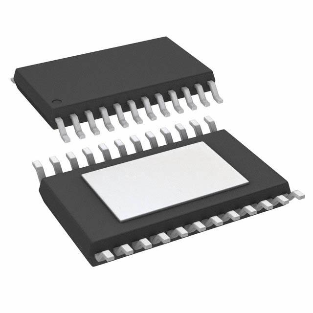


 工商网监
湘ICP备2023018690号
工商网监
湘ICP备2023018690号

