Order
Now
Product
Folder
Support &
Community
Tools &
Software
Technical
Documents
Reference
Design
LM5141-Q1
SNVSAJ6D – JULY 2016 – REVISED DECEMBER 2017
LM5141-Q1 Wide Input Range Synchronous Buck Controller
1 Features
2 Applications
•
•
•
1
•
•
•
•
•
•
•
•
•
•
•
•
•
•
•
•
•
Qualified for Automotive Applications
AEC-Q100 Qualified With the Following Results:
– Device Temperature Grade 1: –40°C to
+125°C Ambient Operating Temperature
– Device HBM ESD Classification Level 2
– Device CDM ESD Classification Level C4B
VIN: 3.8 V to 65 V (70 V Absolute Maximum)
Output: Fixed 3.3 V, 5 V, or Adjustable From
1.5 V to 15 V with ±0.8% Accuracy
Fixed 2.2-MHz or 440-kHz Switching Frequency
with ±5% Accuracy
High-Side and Low-Side Gate Drive With SlewRate Control
Optional Frequency Shift by Varying an Analog
Voltage or RT Resistor
Optional Synchronization to an External Clock
Optional Spread Spectrum
Shutdown Mode IQ: 10 µA Typical
Low Standby Mode IQ: 35 µA Typical
75-mV Current Limit Threshold with ±0.9%
Accuracy
External Resistor or DCR Current Sensing
Output Enable Logic Input
Hiccup Mode for Sustained Overload
Power-Good Indication Output
Selectable Diode Emulation or Forced PulseWidth Modulation
24-pin VQFN Package With Wettable Flanks
Create a Custom Design Using the LM5141-Q1
With the WEBENCH® Power Designer
Automotive Applications Including:
– Infotainment Systems
– Instrumentation Clusters
– Advanced Driver Assistance Systems (ADAS)
3 Description
The LM5141-Q1 is a synchronous buck controller,
intended for high voltage wide VIN step-down
converter applications. The control method is peak
current mode control. Current mode control provides
inherent line feed-forward, cycle-by-cycle current
limiting, and ease-of-loop compensation. The
LM5141-Q1 features slew rate control to simplify the
compliance with CISPR and automotive EMI
requirements.
The LM5141-Q1 has two selectable switching
frequencies: 2.2 MHz and 440 kHz. Gate drivers with
slew rate Control that can be adjusted to reduce EMI.
In light or no-load conditions, the LM5141-Q1
operates in skip cycle mode for improved low power
efficiency. The LM5141-Q1 has a high voltage bias
regulator with automatic switch-over to an external
bias to reduce the IQ current from VIN. Additional
features include frequency synchronization, cycle-bycycle current limit, hiccup mode fault protection for
sustained overload, and power good output.
Device Information(1)
PART NUMBER
LM5141-Q1
PACKAGE
VQFN (24)
BODY SIZE (NOM)
4.00 mm × 4.00 mm
(1) For all available packages, see the orderable addendum at
the end of the data sheet.
Simplified Schematic
VIN
CIN
VCC
VIN
DBST
CVCC
HB
CBST
RES
HO
SS
DITH
CRES
CSS
CDITH
LOUT
HOL
SW
LM5141-Q1
RSENSE
VOUT
COUT
LO
LOL
PGND
PG
CS
EN
DEMB
VOUT
VCCX
RCOMP CCOMP
COMP
AGND
RT
RT
FB
OSC VDDA
CVDDA
Copyright © 2016, Texas Instruments Incorporated
1
An IMPORTANT NOTICE at the end of this data sheet addresses availability, warranty, changes, use in safety-critical applications,
intellectual property matters and other important disclaimers. PRODUCTION DATA.
�LM5141-Q1
SNVSAJ6D – JULY 2016 – REVISED DECEMBER 2017
www.ti.com
Table of Contents
1
2
3
4
5
6
7
Features ..................................................................
Applications ...........................................................
Description .............................................................
Revision History.....................................................
Pin Configuration and Functions .........................
Specifications.........................................................
1
1
1
2
3
4
6.1
6.2
6.3
6.4
6.5
6.6
6.7
4
5
5
5
6
8
9
Absolute Maximum Ratings ......................................
ESD Ratings..............................................................
Recommended Operating Conditions.......................
Thermal Information ..................................................
Electrical Characteristics...........................................
Switching Characteristics ..........................................
Typical Characteristics ..............................................
Detailed Description ............................................ 12
7.1 Overview ................................................................. 12
7.2 Functional Block Diagram ....................................... 12
7.3 Feature Description................................................. 13
8
Application and Implementation ........................ 22
8.1 Application Information............................................ 22
8.2 Typical Application ................................................. 22
9 Power Supply Recommendations...................... 35
10 Layout................................................................... 35
10.1 Layout Guidelines ................................................. 35
10.2 Layout Examples................................................... 36
11 Device and Documentation Support ................. 39
11.1
11.2
11.3
11.4
11.5
11.6
Custom Design With WEBENCH® Tools .............
Receiving Notification of Documentation Updates
Community Resources..........................................
Trademarks ...........................................................
Electrostatic Discharge Caution ............................
Glossary ................................................................
39
39
39
39
39
39
12 Mechanical, Packaging, and Orderable
Information ........................................................... 39
4 Revision History
Changes from Revision C (February 2017) to Revision D
Page
•
Added top navigator icon for TI Design reference design ..................................................................................................... 1
•
Changed "CDS18534Q5A" to "CSD18534Q5A" to fix typo.................................................................................................. 29
•
Changed "+" to "×" in Equation 56 ...................................................................................................................................... 32
Changes from Revision B (January 2017) to Revision C
Page
•
Changed the FBD with updates in the CS pin area ............................................................................................................. 12
•
Updated ISTEP definition in Equation 28 ............................................................................................................................... 25
Changes from Revision A (July 2016) to Revision B
Page
•
Added 'Systems' to the ADAS bullet in Applications ............................................................................................................. 1
•
Changed Description text From: 'conducted EMI' To: 'EMI' ................................................................................................... 1
•
Changed test conditions for RT parameter from: OSC = VDD to: OSC = GND ................................................................... 8
•
Changed equation unit From: '0.815 Apk' To: '0.815 A' ....................................................................................................... 24
•
Changed equation unit From: '6.41 Apk' To: '6.41 A' ........................................................................................................... 24
•
Changed equation unit From: '8.81 Apk' To: ' 8.81 A' .......................................................................................................... 25
•
Changed equation unit From: '0.235 ARMS' To: '0.235 A'...................................................................................................... 26
•
Changed text From: 'a capacitance value greater than filter capacitor CIN' To: 'a capacitance value greater than 5
times the filter capacitor CIN' ................................................................................................................................................ 28
•
Changed equation text From: '62A' and '105 nc' To: '(6A)2' and '105 nC' ............................................................................ 28
•
Added GCS to equation definition list .................................................................................................................................... 31
•
Added Ω and µS symbols to equation text ........................................................................................................................... 33
Changes from Original (July 2016) to Revision A
•
2
Page
Changed Product Preview to Production Data Release ........................................................................................................ 1
Submit Documentation Feedback
Copyright © 2016–2017, Texas Instruments Incorporated
Product Folder Links: LM5141-Q1
�LM5141-Q1
www.ti.com
SNVSAJ6D – JULY 2016 – REVISED DECEMBER 2017
5 Pin Configuration and Functions
RES
EN
SS
PG
COMP
FB
24
23
22
21
20
19
RGE Package
24-Pin VQFN With Exposed Thermal Pad
Top View
DEMB
1
18
CS
VDDA
2
17
VOUT
AGND
3
16
VCCX
15
VIN
Thermal
Pad
11
12
SW
HO
HB
13
10
6
VCC
OSC
9
HOL
PGND
14
8
5
LO
DITH
7
4
LOL
RT
Not to scale
Connect Exposed Pad on bottom to AGND and PGND on the PCB.
Pin Functions
PIN
TYPE
DESCRIPTION
DEMB
I
Diode emulation pin. Connect the DEMB pin to AGND to enable diode emulation. If it is
connected to VDDA the LM5141-Q1 operates in forced PWM (FPWM) mode with continuous
conduction at light loads. The DEMB pin can also be used as a synchronization input, to
synchronize the internal oscillator to an external clock.
2
VDDA
P
Internal analog bias regulator output. Connect a capacitor from the VDDA pin to AGND.
3
AGND
G
Analog ground connection. Ground return for the internal voltage reference and analog
circuits.
4
RT
I
A resistor from the RT pin to ground shifts the oscillator frequency up or down from 2.2 MHz
(1.8 MHz to 2.53 MHz), or 440 kHz (300 kHz to 500 kHz). An analog voltage can be applied
to the RT pin (through a resistor) to shift the oscillator frequency.
NO.
NAME
1
5
DITH
O
A capacitor connected between the DITH pin and AGND is charged and discharged with a
20 µA current source. If Dither is enabled, the voltage on the DITH pin ramps up and down
modulating the oscillator frequency between –5% and +5% of the internal oscillator.
Connecting DITH to VDDA disables the dithering feature. DITH is ignored if an external
synchronization clock is used.
6
OSC
I
Frequency selection pin. Connecting the OSC pin to VDDA sets the oscillator frequency to
2.2 MHz. Connecting the OSC pin to AGND sets the frequency to 440 kHz.
7
LOL
O
Low-side gate driver turnoff output.
8
LO
O
Low-side gate driver turnon output.
9
PGND
G
Power ground connection pin for low-side NMOS gate driver.
10
VCC
P
VCC bias supply pin. Connect a capacitor from the VCC pin to PGND.
11
HB
P
High-side driver supply for bootstrap gate drive.
12
SW
13
HO
O
High-side gate driver turnon output.
14
HOL
O
High-side gate driver turnoff output.
Switching node of the buck regulator. Connect to the bootstrap capacitor, the source terminal
of the high-side MOSFET and the drain terminal of the low-side MOSFET.
Submit Documentation Feedback
Copyright © 2016–2017, Texas Instruments Incorporated
Product Folder Links: LM5141-Q1
3
�LM5141-Q1
SNVSAJ6D – JULY 2016 – REVISED DECEMBER 2017
www.ti.com
Pin Functions (continued)
PIN
NO.
TYPE
NAME
DESCRIPTION
15
VIN
P
Supply voltage input source for the VCC regulator
16
VCCX
P
Optional input for an external bias supply. If VCCX > 4.5 V, VCCX is internally connected to
the VCC pin and the internal VCC regulator is disabled. If VCCX is unused, it should be
grounded.
17
VOUT
I
Current sense amplifier input. Connect this pin to the output side of the current sense
resistor.
18
CS
I
Current sense amplifier input. Make a low current Kelvin connection between this pin and the
inductor side of the external current sense resistor.
19
FB
I
Connect the FB pin to VDDA for a fixed 3.3-V output or connect FB to AGND for a fixed 5-V
output. Connecting the FB pin to the appropriate output divider network will set the output
voltage between 1.5 V and 15 V. The regulation threshold at the FB pin is 1.2 V.
20
COMP
I
Output of the transconductance error amplifier.
21
PG
O
An open collector output which switches low if VOUT is outside of the power good window.
22
SS
I
Soft-start programming pin. An external capacitor and an internal 20-μA current source set
the ramp rate of the internal error amplifier reference during soft-start. Pulling SS pin below
80 mV turns-off the gate driver outputs, but all the other functions remain active.
23
EN
I
An active high logic input enables the controller.
O
Restart timer pin. An external capacitor configures the hiccup mode current limiting. The
capacitor at the RES pin determines the time the controller will remain off before
automatically restarting in hiccup mode. The hiccup mode commences when the controller
experiences 512 consecutive PWM cycles with cycle-by-cycle current limiting. Connecting
the RES pin to VDD during power up disables hiccup mode protection.
24
RES
6 Specifications
6.1 Absolute Maximum Ratings
over operating free-air temperature range (unless otherwise noted) (1)
MIN
MAX
UNIT
VIN
–0.3
70
V
SW to PGND
–0.3
70
V
SW to PGND (20 ns transient)
–5
HB to SW
–0.3
HB to SW (20 ns transient)
–5
HO, HOL to SW
Input voltage
(2)
4
V
V
HB + 0.3
–5
V
V
LO, LOL to PGND
–0.3
LO, LOL to PGND (20 ns transient)
–1.5
OSC, SS, COMP, RES, DEMB, RT, DITH
–0.3
VDD + 0.3
V
EN to PGND
–0.3
70
V
VCC, VCCX, VDD, PG, FB
–0.3
6.5
V
VOUT, CS
–0.3
15.5
V
–0.3
0.3
V
–40
150
°C
–65
150
°C
(2)
Storage temperature, Tstg
(1)
–0.3
HO, HOL to SW (20 ns transient)
PGND to AGND
Operating junction temperature
V
6.5
VCC + 0.3
V
V
Stresses beyond those listed under Absolute Maximum Ratings may cause permanent damage to the device. These are stress ratings
only, which do not imply functional operation of the device at these or any other conditions beyond those indicated under Recommended
Operating Conditions. Exposure to absolute-maximum-rated conditions for extended periods may affect device reliability.
High junction temperatures degrade operating lifetimes. Operating lifetime is de-rated for junction temperatures greater than 125°C.
Submit Documentation Feedback
Copyright © 2016–2017, Texas Instruments Incorporated
Product Folder Links: LM5141-Q1
�LM5141-Q1
www.ti.com
SNVSAJ6D – JULY 2016 – REVISED DECEMBER 2017
6.2 ESD Ratings
VALUE
Human-body model (HBM), per AEC Q100-002 (1)
V(ESD)
(1)
Electrostatic discharge
Charged-device model (CDM), per AEC
Q100-011
UNIT
±2000
All pins except
1,6,7,12,13,18,19, and 24
±500
Pins 1,6,7,12,13,18,19, and
24
±750
V
AEC Q100-002 indicates that HBM stressing shall be in accordance with the ANSI/ESDA/JEDEC JS-001 specification.
6.3 Recommended Operating Conditions
over operating free-air temperature range (unless otherwise noted) (1)
MIN
VIN
VIN
Input voltage
(2)
MAX
UNIT
65
V
SW to PGND
–0.3
65
V
HB to SW
–0.3
HO, HOL to SW
–0.3
LO, LOL to PGND
–0.3
FB, PG, OSC, SS, RES, DEMB,
VCCX
–0.3
EN to PGND
–0.3
VCC, VDD
–0.3
5
1.5
5
VOUT, CS
(1)
NOM
3.8
5
5
5.25
V
HB + 0.3
V
5.25
V
5
V
65
V
5.25
V
15
V
PGND to AGND
–0.3
0.3
V
Operating junction temperature (2)
–40
150
°C
Recommended Operating Conditions are conditions under which the device is intended to be functional. For specifications and test
conditions, see Electrical Characteristics.
High junction temperatures degrade operating lifetimes. Operating lifetime is de-rated for junction temperatures greater than 125°C.
6.4 Thermal Information
LM5141-Q1
THERMAL METRIC (1)
RGE (QFN)
UNIT
24 PINS
RθJA
Junction-to-ambient thermal resistance
34.1
°C/W
RθJC(top)
Junction-to-case (top) thermal resistance
36.8
°C/W
RθJB
Junction-to-board thermal resistance
12.1
°C/W
ψJT
Junction-to-top characterization parameter
0.5
°C/W
ψJB
Junction-to-board characterization parameter
12.2
°C/W
RθJC(bot)
Junction-to-case (bottom) thermal resistance
2.9
°C/W
(1)
For more information about traditional and new thermal metrics, see the Semiconductor and IC Package Thermal Metrics application
report.
Submit Documentation Feedback
Copyright © 2016–2017, Texas Instruments Incorporated
Product Folder Links: LM5141-Q1
5
�LM5141-Q1
SNVSAJ6D – JULY 2016 – REVISED DECEMBER 2017
www.ti.com
6.5 Electrical Characteristics
TJ = –40°C to +125°C, Typical values TJ = 25°C, VIN = 12 V, VCCX = 5 V, VOUT = 5 V, EN = 5 V, OSC = VDD, FSW = 2.2
MHz, no-load on the drive outputs (HO, HOL, LO, and LOL outputs), over operating free-air temperature range (unless
otherwise noted) (1) (2)
PARAMETER
TEST CONDITIONS
MIN
TYP
MAX
UNIT
VIN = 8–18 V, EN = 0 V, VCCX = 0 V
10
12.5
µA
EN = 5 V, FB = VDD, VOUT in
regulation, no-load, not switching,
DEMB = GND.
35
45
EN = 5 V, FB = 0 V, VOUT in
regulation, no-load, not switching,
VCCX = 5 V, DEMB = GND.
42
55
5
5.25
3.4
3.55
VIN SUPPLY VOLTAGE
ISHUTDOWN
ISTANDBY
Shutdown mode current
Standby current
µA
VCC REGULATOR
VCC(REG)
VCC regulation voltage
VIN = 6 to 18 V, 0 to 75 mA, VCCX =
0V
4.75
VCC(UVLO)
VCC undervoltage threshold
VCC rising, VCCX = 0 V
3.25
VCC(HYST)
VCC hysteresis voltage
VCCX = 0 V
ICC(LIM)
VCC sourcing current limit
VCCX = 0 V
Internal bias supply power
VCCX = 0 V
V
V
175
mV
85
125
mA
4.75
5
5.25
3.2
3.3
VDDA
VDDA(REG)
3.1
V
VDDA(UVLO)
VCC rising, VCCX = 0 V
VDDA(HYST)
VCCX = 0 V
125
mV
V
RVDDA
VCCX = 0 V
55
Ω
VCCX
VCCX(ON)
VCC rising
4.1
VCCX(HYST)
R(VCCX)
VCCX = 5 V
4.3
4.4
V
80
mV
2
Ω
OSCILLATOR SELECT THRESHOLDS
Oscillator select threshold 2.2 MHz
(OSC pin)
Oscillator select threshold 440 kHz
(OSC pin)
2.0
V
0.8
V
82
mV
CURENT LIMIT
V(CS)
Current limit threshold
tdly
Current sense delay to output
ILSET = VDDA, measure from CS to
VOUT
75
40
Current sense amplifier gain
ICS(BIAS)
68
11.4
12
Amplifier input bias
ns
12.6
V/V
10
nA
RES
I(RES)
RES current source
20
V(RES)
RES threshold
1.2
µA
V
Timer
Timer hiccup mode fault
512
cycles
RDS(ON)
RES pulldown
4
Ω
OUTPUT VOLTAGE REGULATION
3.3 V
VIN = 3.8 to 42 V
3.273
3.3
3.327
V
5V
VIN = 5.5 to 42 V
4.96
5.0
5.04
V
1.2
1.207
FEEDBACK
(1)
(2)
6
VOUT select threshold 3.3 V
VDD - 0.3
Regulated feedback voltage
1.193
V
V
All minimum and maximum limits are specified by correlating the electrical characteristics to process and temperature variations and
applying statistical process control.
The junction temperature (TJ in ºC) is calculated from the ambient temperature (TA in ºC) and power dissipation (PD in Watts) as follows:
TJ = TA + (PD × RθJA) where RθJA (in °C/W) is the package thermal impedance provided in the Thermal Information section.
Submit Documentation Feedback
Copyright © 2016–2017, Texas Instruments Incorporated
Product Folder Links: LM5141-Q1
�LM5141-Q1
www.ti.com
SNVSAJ6D – JULY 2016 – REVISED DECEMBER 2017
Electrical Characteristics (continued)
TJ = –40°C to +125°C, Typical values TJ = 25°C, VIN = 12 V, VCCX = 5 V, VOUT = 5 V, EN = 5 V, OSC = VDD, FSW = 2.2
MHz, no-load on the drive outputs (HO, HOL, LO, and LOL outputs), over operating free-air temperature range (unless
otherwise noted)(1)(2)
PARAMETER
FB(LOWRES)
Resistance to ground on FB for FB
= 0 detection
FB(EXTRES)
Thevenin equivalent resistance at
FB for external regulation detection
TEST CONDITIONS
FB < 2 V
MIN
TYP
MAX
UNIT
500
Ω
5
kΩ
TRANSCONDUCTANCE AMPLIFIER
Gm
Gain
Feedback to COMP
1010
1200
Input bias current
µS
15
nA
Transconductance amplifier source
current
COMP = 1 V, FB = 1 V
100
µA
Transconductance amplifier sink
current
COMP = 1 V, FB = 1.4 V
100
µA
POWER GOOD
PG(UV)
PG undervoltage trip levels
Falling with respect to the regulation
voltage
90%
92%
94%
PG(OVP)
PG overvoltage trip levels
Rising with respect to the regulation
voltage
108%
110%
112%
PG(VOL)
PG
Open collector, Isink = 2 mA
PG(rdly)
OV filter time
VOUT rising
25
µs
PG(fdly)
UV filter time
VOUT falling
30
µs
PG(HYST)
3.4%
0.4
V
HO GATE DRIVER
VOLH
HO Low-state output voltage
IHO = 100 mA
0.05
V
VOHH
HO High-state output voltage
IHO = –100 mA, VOHH = VHB - VHO
0.07
V
trHO
HO rise time (10% to 90%)
CLOAD = 2700 pf
4
ns
tfHO
HO fall time (90% to 10%)
CLOAD = 2700 pf
3
ns
IOHH
HO peak source current
VHO = 0 V, SW = 0 V, HB = 5 V,
VCCX = 5 V
3.25
Apk
IOLH
HO peak sink current
VCCX = 5 V
4.25
Apk
UVLO
HO falling
V(BOOT)
I(BOOT)
Hysteresis
Quiescent current
2.5
V
110
mV
3
µA
V
LO GATE DRIVER
VOLL
LO Low-state output voltage
ILO = 100 mA
0.05
VOHL
LO High-state output voltage
ILO = –100 mA, VOHL = VCC – VLO
0.07
V
trLO
LO rise time (10% to 90%)
CLOAD = 2700 pf
4
ns
tfLO
LO fall time (90% to 10%)
CLOAD = 2700 pf
3
ns
IOHL
LO peak source current
VCCX = 5 V
3.25
Apk
IOLL
LO peak sink current
VCCX = 5 V
4.25
Apk
2.5
V
ADAPTIVE DEAD TIME CONTROL
V(GS-DET)
VGS detection threshold
VGS falling, no load
tdly1
HO off to LO on dead time
20
40
ns
tdly2
LO off to HO on dead time
20
38
ns
0.8
V
DIODE EMULATION
VIL
DEMB input low threshold
VIH
FPWM input high threshold
SW
Zero cross threshold
2
V
–5
Submit Documentation Feedback
Copyright © 2016–2017, Texas Instruments Incorporated
Product Folder Links: LM5141-Q1
mV
7
�LM5141-Q1
SNVSAJ6D – JULY 2016 – REVISED DECEMBER 2017
www.ti.com
Electrical Characteristics (continued)
TJ = –40°C to +125°C, Typical values TJ = 25°C, VIN = 12 V, VCCX = 5 V, VOUT = 5 V, EN = 5 V, OSC = VDD, FSW = 2.2
MHz, no-load on the drive outputs (HO, HOL, LO, and LOL outputs), over operating free-air temperature range (unless
otherwise noted)(1)(2)
PARAMETER
TEST CONDITIONS
MIN
TYP
MAX
UNIT
ENABLE INPUT
VIL
Enable input low threshold
VCCX = 0 V
VIH
Enable input high threshold
VCCX = 0 V
IIkg
Leakage
EN logic input only
0.8
2.0
V
V
1
µA
SYN INPUT (DEMB pin)
VIL
DEMB input low threshold
VIH
DEMB input high threshold
0.8
2
V
V
DEMB input low frequency range
440 kHz
350
550
kHz
DEMB input high frequency range
2.2 MHz
1800
2600
kHz
DITHER
IDITHER
Dither source/sink current
20
µA
VDITHER
Dither high threshold
1.26
V
Dither low threshold
1.14
V
SOFT-START
ISS
Soft-Start current
RDS(ON)
Soft-Start pull-down resistance
16
22
28
µA
3
Ω
175
ºC
15
ºC
THERMAL
TSD Thermal Shutdown
Thermal shutdown hysteresis
6.6 Switching Characteristics
over operating free-air temperature range (unless otherwise noted)
PARAMETER
RT
MIN
TYP
MAX
UNIT
Oscillator Frequency 2.2 MHz
OSC = VDDA, VIN = 8–18 V
2100
2200
2300
kHz
Oscillator Frequency 440 kHz
OSC = GND, VIN = 8–18 V
420
440
460
kHz
Adjustment
Range
2.2 MHz
RT
Adjustment
Range
TEST CONDITIONS
Minimum
OSC = VDD, RTMIN = 61.9 kΩ
1710
1800
1890
kHz
Typical
OSC = VDD, RTTYP = 49.9 kΩ
2100
2200
2300
kHz
Maximum
OSC = VDD, RTMAX = 43.2 kΩ
2405
2530
2655
kHz
Minimum
OSC = GND, RTMIN = 73.2 k
285
300
315
kHz
Typical
OSC = GND, RTTYP = 49.9 kΩ
420
440
460
kHz
440 kHz
Maximum
OSC = GND, RTMAX = 44.2 kΩ
475
500
525
kHz
RT
Response
time
RT= 61.9–43.2 kΩ
RT
Response
time
RT = 43.2–61.9 kΩ
RT
2
µs
3.5
µs
Response
time
16
µs
ton
Minimum on-time
45
toff
Minimum off-time
8
Submit Documentation Feedback
66
ns
100
ns
Copyright © 2016–2017, Texas Instruments Incorporated
Product Folder Links: LM5141-Q1
�LM5141-Q1
www.ti.com
SNVSAJ6D – JULY 2016 – REVISED DECEMBER 2017
6.7 Typical Characteristics
100
100
90
90
80
80
Efficiency (%)
Efficiency (%)
At TA = 25ºC, unless otherwise noted
70
60
50
70
60
50
40
40
VIN 8 V
VIN 12 V
VIN 18 V
30
VIN 8 V
VIN 12 V
VIN 18 V
30
20
20
0
0.5
1
1.5
2
2.5
3
3.5
Output Current (A)
VIN 8–18 V
VOUT 5 V
4
4.5
0
5
0.5
1
EN = 12 V
FPWM
2.2 MHz
2
2.5
3
3.5
Output Current (A)
VIN 8–18 V
VOUT 5 V
Figure 1. Efficiency vs IOUT
4
5
D002
EN = 12 V
DEMB
2.2 MHz
Figure 2. Efficiency vs IOUT
125qC
25qC
-40qC
65
60
10
ISHUTDOWN (PA)
55
50
45
40
8
6
4
35
VIN 8 V
VIN 12 V
VIN 18 V
2
30
0
-50
25
8
9
10
11
12
13
14
VIN (V)
15
16
17
18
-30
-10
10
D003
EN = 12 V
30
50
70
90
Temperature (qC)
110
130
150
D004
D001
VIN 8–18 V
Figure 3. ISTANDBY vs VIN
EN = 0 V
Figure 4. ISHUTDOWN vs Temperature
5.25
3.50
5.20
3.48
5.15
3.46
5.10
3.44
VCC (UVLO) (V)
VCC ( REG) (V)
4.5
12
70
ISTANDBY (PA)
1.5
D001
5.05
5.00
4.95
3.42
3.40
3.38
4.90
3.36
4.85
3.34
4.80
3.32
4.75
3.30
6
7
8
9
10
11
12
13
14
15
VIN (V)
VIN 6-18 V
EN = GND
16
17
18
-60
-40
-20
0
20
40
60
80
100
120
Temperature (°C)
D005
VIN 8–18 V
Figure 5. VCC(REG) vs VIN
140
D006
EN = 12 V
Figure 6. VCC(UVLO) vs Temperature
Submit Documentation Feedback
Copyright © 2016–2017, Texas Instruments Incorporated
Product Folder Links: LM5141-Q1
9
�LM5141-Q1
SNVSAJ6D – JULY 2016 – REVISED DECEMBER 2017
www.ti.com
Typical Characteristics (continued)
5.25
3.30
5.20
3.28
5.15
3.26
5.10
3.24
VDDA (UVLO) (V)
VDDA (REG) (V)
At TA = 25ºC, unless otherwise noted
5.05
5.00
4.95
3.22
3.20
3.18
4.90
3.16
4.85
3.14
4.80
3.12
4.75
3.10
-60
-40
-20
0
20
40
60
80
100
120
140
Temperature (°C)
VCC Rising
-60
-40
EN = 12 V
VCC Rising
13.00
4.45
12.80
4.40
12.60
CS Amplifier Gain (V/V)
VCCX (ON) (V)
20
40
60
80
100
120
140
D008
EN = 12 V
Figure 8. VDD(UVLO) vs Temperature
4.50
4.35
4.30
4.25
4.20
4.15
4.10
12.40
12.20
12.00
11.80
11.60
11.40
4.05
11.20
4.00
-60
-40
-20
0
20
40
60
80
100
120
VCC Rising
11.00
-60
140
Temperature (°C)
-40
-20
0
D009
EN = 12 V
20
40
60
80
Temperature (qC)
100
120
140
D010
VIN 12 V
Figure 9. VCCX(ON) vs Temperature
EN = 12 V
Figure 10. Current Sense Amplifier Gain vs Temperature
3.32
5.000
+125qC
+25qC
-40qC
3.31
3.3
+125qC
+25qC
-40qC
4.995
4.990
3.29
Output Voltage (V)
Output Voltage (V)
0
Temperature (°C)
Figure 7. VDD(REG) vs Temperature
3.28
3.27
3.26
3.25
4.985
4.980
4.975
4.970
4.965
3.24
4.960
3.23
4.955
3.22
4.950
0
0.5
1
VIN 12 V
1.5
2
2.5
3
3.5
Output Current (A)
FB = VDDA
4
4.5
5
0
0.5
1
D011
EN = 12 V
Figure 11. 3.3-V Output Voltage Regulation vs IOUT
10
-20
D007
VIN 12 V
1.5
2
2.5
3
3.5
Output Current (V)
EN = 12 V
4
4.5
5
D012
FB = GND
Figure 12. 5-V Output Voltage Regulation vs IOUT
Submit Documentation Feedback
Copyright © 2016–2017, Texas Instruments Incorporated
Product Folder Links: LM5141-Q1
�LM5141-Q1
www.ti.com
SNVSAJ6D – JULY 2016 – REVISED DECEMBER 2017
Typical Characteristics (continued)
At TA = 25ºC, unless otherwise noted
2400
470
465
2340
460
Frequency (KHz)
Frequency (KHz)
455
2280
2220
2160
450
445
440
435
430
425
2100
420
415
2040
-60
-40
-20
0
20
40
60
80
Temperature (qC)
VIN 12 V
100
120
410
-60
140
EN = 12 V
OSC = VDDA
0
20
40
60
80
Temperature (qC)
100
120
140
D014
EN = 12 V
OSC = AGND
Figure 14. 440-kHz Oscillator Frequency vs Temperature
90
110
80
105
100
70
95
toff(ns)
60
50
40
90
85
80
30
75
20
70
10
65
0
-60
-40
-20
0
20
40
60
80
Temperature (qC)
100
120
60
-60
140
-40
0
20
40
60
80
Temperature (qC)
VIN 3.8 V
Figure 15. ton Minimum vs Temperature
100
120
140
D016
VOUT 3.3 V
Figure 16. toff Minimum vs Temperature
600
2500
560
2400
520
2300
480
Frequency (KHz)
2600
2200
2100
2000
1900
1800
440
400
360
320
280
1700
1600
-60
-20
D015
VIN 18 V
Frequency (KHz)
-20
VIN 12 V
Figure 13. 2.2-MHz Oscillator Frequency vs Temperature
ton (ns)
-40
D013
RT 49.9 kΩ
-40
-20
0
RT 43.2 kΩ
20
40
60
Temperature (°C)
240
RT 61.9 kΩ
80
100
120
140
RT 49.9 k:
200
-60
-40
-20
D017
VIN 12 V
0
RT 44.2 k:
20
40
60
80
Temperature (qC)
RT 73.2 k:
100
120
140
D018
VIN 12 V
Figure 17. RT Frequency vs Temperature (2.2 MHz)
Figure 18. RT Frequency vs Temperature (440 kHz)
Submit Documentation Feedback
Copyright © 2016–2017, Texas Instruments Incorporated
Product Folder Links: LM5141-Q1
11
�LM5141-Q1
SNVSAJ6D – JULY 2016 – REVISED DECEMBER 2017
www.ti.com
7 Detailed Description
7.1 Overview
The LM5141-Q1 is a switching controller that features all of the functions necessary to implement a highefficiency buck power supply that can operate over a wide input-voltage range. The LM5141-Q1 is configured to
provide a single fixed 3.3-V or 5-V output, or an adjustable output between 1.5 V to 15 V. This easy-to-use
controller integrates high-side and low-side MOSFET drivers capable of sourcing 3.25 A and sinking 4.25 A
peak. The control method is current mode control, which provides inherent line feed-forward, cycle-by-cycle
current limiting, and ease-of-loop compensation. With the OSC pin connected to VDD, the default oscillator
frequency is 2.2 MHz. With the OSC pin grounded, the oscillator frequency is 440 kHz. The LM5141-Q1 can be
synchronized by applying an external clock to the DEMB pin. Fault protection features include current limiting,
thermal shutdown, and remote shutdown capability.
The LM5141-Q1 incorporates features that simplify compliance with the CISPR and automotive EMI
requirements. The LM5141-Q1 has optional spread spectrum to reduce the peak EMI and gate drivers with slewrate control. The QFN-24 package features an exposed pad to aid in thermal dissipation.
7.2 Functional Block Diagram
VIN
VCCX
VREF 1.2 V
BIAS
VCC
VDDA
CONTROL
VDDA
20 uA
RESTART
LOGIC
RES
CL
HICCUP FAULT
TIMER 256 CYCLES
CLK
OUT
CURRENT
LIMIT
Gain = 12
75 mV
+
CS
VOUT
DEMB
DEMB/
FPWM/
SYNIN
EN
CL
OSC
RT
DITH
+
SLOPE
COMPENSATION
RAMP
3.3 V
HB1 UVLO
HB
5V
VOUT
DECODER/
MUX
+
DEMB
HO
HOL
OUT
FB
+
STBY
SSCOMPLETE
FBi
20 uA
VREF
SS
R
Q
S
Q
PWM
1200 uS
CLK
LEVEL SHIFT
ADAPTIVE
DEAD TIME
SW
VCC
LO
LOL
+
+
SS
SS
PGND
COMP
1.356 V STBY
AGND
PGOV
PGDLY
25 us
+
PG
STAND-BY
PGUV
1.056 V
VSTBY
+
+
+
Copyright © 2016, Texas Instruments Incorporated
12
Submit Documentation Feedback
Copyright © 2016–2017, Texas Instruments Incorporated
Product Folder Links: LM5141-Q1
�LM5141-Q1
www.ti.com
SNVSAJ6D – JULY 2016 – REVISED DECEMBER 2017
7.3 Feature Description
7.3.1 High Voltage Start-up Regulator
The LM5141-Q1 contains an internal high voltage VCC bias regulator that provides the bias supply for the PWM
controller and the gate drivers for the external MOSFETs. The input pin (VIN) can be connected directly to an
input voltage source up to 65 V. The output of the VCC regulator is set to 5 V. When the input voltage is below
the VCC set-point level, the VCC output will track VIN with a small voltage drop. In high voltage applications
extra care should be taken to ensure the VIN pin does not exceed the absolute maximum voltage rating of 70 V
including line or load transients. Voltage ringing on the VIN pin that exceeds the absolute maximum ratings can
damage the IC. Use a high quality bypass capacitor between VIN and ground to minimize ringing.
7.3.2 VCC Regulator
The VCC regulator output current limit is 75 mA (minimum). At power-up, the regulator sources current into the
capacitors connected to the VCC pin. When the voltage on the VCC pin exceeds 3.4 V the output is enabled and
the soft-start sequence begins. The output remains active unless the voltage on the VCC pin falls below the
VCC(UVLO) threshold of 3.2 V (typical) or the enable pin is switched to a low state. The recommended range for
the VCC capacitor is 2.2 µF to 4.7 µF
An internal 5-V linear regulator generates the VDDA bias supply. Bypass VDDA with a 100-nF or greater ceramic
capacitor to ensure a low noise internal bias rail. Normally VDDA is 5 V, but there are two operating conditions
where it regulates at 3.3 V. The first is in skip cycle mode with VOUT of 3.3 V. The second is when VIN is less
than 5 V. Under these conditions both VCC and VDD drop below 5 V. Internal power dissipation in the VCC
Regulator can be minimized by connecting the VCCX pin to a 5-V output or to an external 5-V supply. If VCCX >
4.5 V, VCCX is internally connected to VCC and the internal VCC regulator is disabled. If VCCX is unused, it
should be grounded. Never connect the VCCX pin to a voltage greater than 6.5 V.
7.3.3 Oscillator
The LM5141-Q1 has an internal trimmed oscillator with two frequency options: 2.2 MHz, or 440 kHz. With the
OSC pin connected to VDDA the oscillator frequency is 2.2 MHz. With the OSC pin grounded, the oscillator
frequency is 440 kHz. The state of the OSC pin is read and latched during VCC power-up and cannot be
changed until VCC drops below the VCC(UVLO) threshold.
The oscillator frequency can be modulated up or down from the nominal oscillator frequency (2.2 MHz or 440
kHz) on demand by connecting a resistor from the RT pin to ground (refer to Figure 19). To disable the
frequency modulation option, the RT pin can be grounded or left open. If the RT pin is connected to ground
during power-up the frequency modulation option is latch-off and cannot be changed unless VCC is allowed to
drop below the VCC(UVLO) threshold. If the RT pin is left open during power-up the frequency modulation option
will be disabled, but it can be enabled at a later time by switching in a valid RT resistor. When the frequency
modulation option is disabled, the LM5141-Q1 will operate at the internal oscillator frequency (2.2 MHz or 440
kHz).
On power up, after soft-start is complete and the output voltage is in regulation, a 16-µs timer is initiated. If a
valid RT resistor is connected, the LM5141-Q1 will switch to the frequency set by the RT resistor n the
completion of the 16-µs time delay.
The modulation range for 2.2 MHz is 1.8 MHz to 2.53 MHz (refer to Table 1). If an RT resistor value > 95 kΩ
(typical) is placed on the RT pin, the LM5141-Q1 controller will assume that the RT pin is open, and will use the
internal oscillator. If an RT resistor < 27 kΩ (typical) is connected, the controller will use the internal oscillator. To
calculate an RT resistor for a specific oscillator frequency, use Equation 1 for the 2.2 MHz frequency range or
Equation 2 for the 440 kHz frequency range.
1
- 0.0216
RT2.2 MHz Fsw
0.0086
where
•
RT is kΩ and Fsw is in MHz
(1)
Submit Documentation Feedback
Copyright © 2016–2017, Texas Instruments Incorporated
Product Folder Links: LM5141-Q1
13
�LM5141-Q1
SNVSAJ6D – JULY 2016 – REVISED DECEMBER 2017
www.ti.com
Feature Description (continued)
RT440 kHz
1
- 1.38 u 10-5
Fsw
4.5 u 10-5
where
•
RT is in kΩ and Fsw is in kHz
(2)
Table 1. RT Resistance vs Oscillator Frequency
S1
S2
RT RESISTANCE
(TYPICAL) 2.2 MHz
2.2 MHZ OSCILLATOR
RANGE (TYPICAL)
RT RESISTANCE
(TYPICAL) 440 kHz
440 kHz OSCILLATOR
RANGE (TYPICAL)
X
X
> 95 kΩ
internal oscillator
> 95 kΩ
internal oscillator
OFF
OFF
61.98 kΩ total
1.8 MHz
73.8 kΩ total
300 kHz
OFF
ON
50.18 kΩ total
2.2 MHz
50.1 kΩ total
440 kHz
ON
OFF
43.2 kΩ
2.53 MHz
44.2 kΩ
500 kHz
X
X
< 27 kΩ
internal oscillator
< 27 kΩ
internal oscillator
LM5141-Q1
VDDA
OSC
RT
43.2 k
S1
6.98 k
S2
11.8 k
Copyright © 2016, Texas Instruments Incorporated
Figure 19. RT Connection Circuit, 2.2 MHz
LM5141-Q1
OSC
RT
44.2 k
S1
S2
5.9 k
23.7 k
Copyright © 2016, Texas Instruments Incorporated
Figure 20. RT Connection Circuit, 440 kHz
14
Submit Documentation Feedback
Copyright © 2016–2017, Texas Instruments Incorporated
Product Folder Links: LM5141-Q1
�LM5141-Q1
www.ti.com
SNVSAJ6D – JULY 2016 – REVISED DECEMBER 2017
An alternative method to modulate the oscillator frequency is to use an analog voltage connected to the RT pin
through a resistor. See Figure 21. An analog voltage of 0.0 V to 0.6 V modulates the oscillator frequency
between 1.8 MHz to 2.53 MHz (OSC at 2.2 MHz), or 300 kHz to 500 kHz (OSC at 440 kHz). The analog voltage
source must be able to sink current.
DEM/SYNC
LM5141-Q1
OSC
RT
44.2 k
0V±6V
Copyright © 2016, Texas Instruments Incorporated
Figure 21. Analog Voltage Control of the Oscillator Frequency
When the LM5141-Q1 is in the low IQ standby mode, the controller sets the RT pin to a high impedance state
and ignores the RT resistor. After coming out of standby mode, the controller will monitor the RT pin. If a valid
resistor is connected, and there have been 16 µs of continuous switching without a zero-crossing event, the
LM5141-Q1 will switch to the frequency set by the RT resistor.
7.3.4 Synchronization
To synchronize the LM5141-Q1 to an external source, apply a logic level clock signal to the DEMB pin. The
synchronization range is 350 kHz to 550 kHz when the internal oscillator is set to 440 kHz. When the internal
oscillator is set to 2.2 MHz, the synchronization range is 1.8 MHz to 2.6 MHz. If there is a valid RT resistor and a
synchronization signal, the LM5141-Q1 with ignore the RT resistor and synchronize the controller to the external
clock. Under low VIN conditions, when the minimum toff time is reached (100ns), the synchronization clock will be
ignored to allow the frequency to drop to maintain output voltage regulation.
7.3.5 Frequency Dithering (Spread Spectrum)
The LM5141-Q1 provides a frequency dithering option that is enabled by connecting a capacitor from the DITH
pin to AGND. A triangular waveform centered at 1.2 V is generated across the CDITH capacitor. Refer to
Figure 22. The triangular waveform modulates the oscillator frequency by ±5% of the nominal frequency set by
the OSC pin or by an RT resistor. The CDITH capacitance value sets the rate of the low frequency modulation. A
lower CDITH capacitance will modulate the oscillator frequency at a faster rate than a higher capacitance. For the
dithering circuit to effectively reduce the peak EMI, the modulation rate must be less than the oscillator frequency
(FSW). Equation 3 calculates the DITH pin capacitance required to set the modulation frequency, FMOD.
20 PA
CDITH
2 u FMOD u 0.12 V
(3)
If the DITH pin is connected to VDDA during power-up the dither feature is latch-off and cannot be changed
unless VCC is allowed to drop below the VCC(UVLO) threshold. If the DITH pin is connected to ground on power
up, dither will be disabled, but it can be enabled by raising the DITH pin voltage above ground and connecting it
to CDITH. When the LM5141 is synchronized to an external clock, Dither is disabled.
Submit Documentation Feedback
Copyright © 2016–2017, Texas Instruments Incorporated
Product Folder Links: LM5141-Q1
15
�LM5141-Q1
SNVSAJ6D – JULY 2016 – REVISED DECEMBER 2017
www.ti.com
1.26 V +5%
1.2 V
1.14 V -5%
DITH
CDITH
LM5141-Q1
Copyright © 2016, Texas Instruments Incorporated
Figure 22. Dither Operation
7.3.6 Enable
The LM5141-Q1 has an enable input EN for start-up and shutdown control of the output. The EN pin can be
connected to a voltage as high as 70 V. If the enable input is greater than 2 V the output is enabled. If the enable
pin is pulled below 0.8 V, the output will be in shutdown, and the LM5141-Q1 is switched to a low IQ shutdown
mode, with a 10-µA typical current drawn from the VIN pin. It is not recommended to leave the EN pin left
floating.
7.3.7 Power Good
The LM5141-Q1 includes an output voltage monitoring function to simplify sequencing and supervision. The
power-good function can be used to enable circuits that are supplied by the output voltage rail or to turn on
sequenced supplies. The PG pin switches to a high impedance state when the output voltage is in regulation.
The PG signal switches low when the output voltage drops below the lower power good threshold (92% typical)
or rises above the upper power good threshold (110% typical). A 25-μs deglitch filter prevents any false tripping
of the power good signal due to transients. TI recommends a pullup resistor of 10 kΩ from the PG pin to the
relevant logic rail. Power good is asserted low during soft start and when the buck converter is disabled by EN.
7.3.8 Output Voltage
The LM5141-Q1 output can be configured for one of the two fixed output voltages with no external feedback
resistors, or the output can be adjusted to the desired voltage using an external resistor divider. VOUT can be
configured as a 3.3-V output by connecting the FB pin to VDDA, or a 5-V output by connecting the FB pin to
ground with a maximum resistance of 500 Ω. The FB connections (either VDDA or GND) are detected during
power up.
The configuration setting is latched and cannot be changed until the LM5141-Q1 is powered down with VCC
falling below VCC(UVLO) (3.4 V typical) and then powered up again.
Alternatively the output voltage can be set using an external resistive dividers from the output to the FB pin. The
output voltage adjustment range is between 1.5 V and 15 V. The regulation threshold at the FB pin is 1.2 V
(VREF). To calculate RFB1 and RFB2 use Equation 4. Refer to Figure 23:
RFB2
§ VOUT ·
- 1¸ u RFB1
¨
© VREF ¹
(4)
The recommend starting point is to select RFB1 between 10 kΩ to 20 kΩ.
The Thevenin equivalent impedance of the resistive divider connected to the FB pin must be greater than 5 kΩ
for the LM5141-Q1 to detect the divider and set the controller to the adjustable output mode. Refer to Equation 5.
RFB1 u RFB2
RTH
! 5 k:
RFB1 RFB2
(5)
16
Submit Documentation Feedback
Copyright © 2016–2017, Texas Instruments Incorporated
Product Folder Links: LM5141-Q1
�LM5141-Q1
www.ti.com
SNVSAJ6D – JULY 2016 – REVISED DECEMBER 2017
If a low IQ mode is required, take care when selecting the external resistors. The extra current drawn from the
external divider is added to the LM5141-Q1 ISTANDBY current (35 μA typical). The divider current reflected to VIN
is divided down by the ratio of VOUT/VIN. For example, if VIN is 12 V and VOUT is set to 5.5 V with RFB1 10 kΩ, and
RFB2 = 35.7 kΩ, the input current at VIN required to supply the current in the feedback resistors is:
VOUT
V
5.5 V
5.5 V
IDIVIDER
u OUT
u
55.16 PA
RFB1 RFB2
VIN
10 k 35.7 k 12 V
where
•
VIN = 12 V
(6)
The total input current in this condition is:
IVIN | ISTANDBY IDIVIDER | 35 PA 55.16 P | 90.16 PA
(7)
LOUT
VOUT
COUT
RFB2
LM5141 Transconductance Amplifier
gm 1200 uS
FB
_
RFB1
VREF
+
SS
+
COMP
Copyright © 2016, Texas Instruments Incorporated
Figure 23. Voltage Feedback
7.3.8.1 Minimum Output Voltage Adjustment
There are two limitations to the minimum output voltage adjustment range: the LM5141-Q1 voltage reference of
1.2 V and the minimum switch node pulse width, tSW.
The minimum controllable on-time at the switch node (tSW) limits the voltage conversion ratio (VOUT/VIN). For
fixed-frequency PWM operation, the voltage conversion ratio should meet the following condition:
VOUT
> t sw × Fsw
VIN
where
•
•
tSW is 70 ns (typical)
FSW is the switching frequency
(8)
If the desired voltage conversion ratio does not meet the above condition, the controller transitions from fixed
frequency operation into a pulse skipping mode to maintain regulation of the output voltage.
For example if the desired output voltage is 3.3 V with a VIN of 20 V and operating at 2.2 MHz, the voltage
conversion ratio test is satisfied:
3.3 V
! 70 ns u2.2MHz
20 V
(9)
0.165 > 0.154
For wide VIN applications and lower output voltages, an alternative is to use the LM5141-Q1 with a 440-kHz
oscillator frequency. Operating at 440 kHz, the limitation of the minimum tSW time is less significant. For example,
if a 1.8-V output is required with a VIN of 50 V:
1.8 V
! 70 ns u 440 kHz
50 V
(10)
0.036 > 0.0308
Submit Documentation Feedback
Copyright © 2016–2017, Texas Instruments Incorporated
Product Folder Links: LM5141-Q1
17
�LM5141-Q1
SNVSAJ6D – JULY 2016 – REVISED DECEMBER 2017
www.ti.com
7.3.9 Current Sense
There are two methods to sense the inductor current of the buck converter. The first is using current sense
resistor in series with the inductor and the second is to use the dc resistance of the inductor (DCR sensing).
Figure 24 shows inductor current sensing using a current-sense resistor. This configuration continuously
monitors the inductor current providing accurate current-limit protection. For the best current-sense accuracy and
overcurrent protection, use a low inductance ±1% tolerance current-sense resistor between the inductor and
output, with a Kelvin connection to the LM5141-Q1 sense amplifier.
If the peak differential current signal sensed from CS to VOUT exceeds 75 mV, the current limit comparator
immediately terminates the HO output for cycle-by-cycle current limiting.
RSENSE
V CS
§
¨ IOUT MAX
©
'I ·
2 ¸¹
where
•
V(CS) = 75 mV
(11)
IOUT(MAX) is the overcurrent setpoint, which is set higher than the maximum load current to avoid tripping the over
current comparator during load transients. ΔI is the peak-peak inductor ripple current.
VOUT
RSENSE
LOUT
COUT
LM5141 Current Sense Amplifier
CS
Gain = 12
+
VOUT
_
Copyright © 2016, Texas Instruments Incorporated
Figure 24. Current Sense
7.3.10 DCR Current Sensing
For high-power applications which do not require high accuracy current-limit protection, DCR sensing may be
preferable. This technique provides lossless and continuous monitoring of the output current using an RC sense
network in parallel with the inductor. Using an inductor with a low DCR tolerance, the user can achieve a typical
current limit accuracy within the range of ±10% to ±15% at room temperature.
Components RCS and CCS in Figure 25 create a low-pass filter across the inductor to enable differential sensing
of the voltage drop across inductor DCR. When RCS × CCS is equal to LOUT/RDCR, the voltage developed across
the sense capacitor, CCS, is a replica of the inductor DCR voltage waveform. Choose the capacitance of CCS to
be greater than 0.1 μF to maintain a low impedance sensing network, thus reducing the susceptibility of noise
pickup from the switch node. Carefully observe the PCB layout guidelines to ensure the noise and DC errors do
not corrupt the differential current-sense signals applied across the CS and VOUT pins.
The voltage drop across CCS:
sLOUT
RDCR
Ipk u RDCR
1 sRCS CCS
1
VCS s
18
(12)
Submit Documentation Feedback
Copyright © 2016–2017, Texas Instruments Incorporated
Product Folder Links: LM5141-Q1
�LM5141-Q1
www.ti.com
SNVSAJ6D – JULY 2016 – REVISED DECEMBER 2017
VOUT
LOUT
RDCR
COUT
CCS
LM5141 Current Sense Amplifier
RCS
CS
Gain = 12
+
VOUT
_
Copyright © 2016, Texas Instruments Incorporated
Figure 25. DCR Current Sensing
RCSCCS = LOUT/RDCR → accurate DC and AC current sensing
If the RC time constant is not equal to the LOUT/LDRC time constant there will be an error
RCSCCS > LOUT/RDCR → DC level still correct, the AC amplitude will be attenuated
RCSCCS < LOUT/RDCR→ DC level still correct, the AC amplitude will be amplified
7.3.11 Error Amplifier and PWM Comparator
The LM5141-Q1 has a high-gain transconductance amplifier that generates an error current proportional to the
difference between the feedback voltage and an internal precision reference (1.2 V). The output of the
transconductance amplifier is connected to the COMP pin allowing the user to provide external control loop
compensation. Generally for current mode control a type II network is recommended.
7.3.12 Slope Compensation
The LM5141-Q1 provides internal slope compensation to ensure stable operation with a duty cycle greater than
50%. To correctly use the internal slope compensation, the inductor value must be calculated based on the
following guidelines (Equation 12 assumes an inductor ripple current of 30%):
VOUT
LOUT t
Fsw u 0.3 u IOUT
(13)
•
•
Lower inductor values increase the peak-to-peak inductor current, which minimizes size and cost and
improves transient response at the cost of reduced efficiency due to higher peak currents.
Higher inductance values decrease the peak-to-peak inductor current typically increases efficiency by
reducing the RMS current at the cost of requiring larger output capacitors to meet load-transient
specifications.
7.3.13 Hiccup Mode Current Limiting
The LM5141-Q1 includes an optional hiccup mode protection function that is enabled when a capacitor is
connected to the RES pin. In normal operation the RES capacitor is discharged to ground. If 512 consecutive
cycles of cycle-by-cycle current limiting occur, the SS pin capacitor is pulled low and the HO and LO outputs are
disabled (refer to Figure 26). A 20-μA current source begins to charge the RES capacitor.
When the RES pin charges to 1.2 V, the RES pin is pulled low, and the SS capacitor begins to charge. The 512
cycle hiccup counter is reset if 4 consecutive switching cycles occur without exceeding the current limit threshold.
The controller is in forced PWM (FPWM) continuous conduction mode when the DEMB pin is connected to
VDDA. In this mode the SS pin is clamped to a level 200 mV above the feedback voltage to the internal error
amplifier. This ensures that SS can be pulled low quickly during a brief overcurrent event and prevent overshoot
of VOUT when the overcurrent condition is removed.
Submit Documentation Feedback
Copyright © 2016–2017, Texas Instruments Incorporated
Product Folder Links: LM5141-Q1
19
�LM5141-Q1
SNVSAJ6D – JULY 2016 – REVISED DECEMBER 2017
www.ti.com
If DEMB = 0 V, the controller operates in diode emulation with light loads (discontinuous conduction mode) and
the SS pin is allowed to charge to VDDA. This reduces the quiescent current of the LM5141-Q1. If 32 or more
cycle-by-cycle current limit events occur, the SS pin is clamped to 200 mV above the feedback voltage to the
internal error amplifier until the hiccup counter is reset. Thus, if a momentary overload occurs that causes at least
32 cycles of current limiting, the SS capacitor voltage will be slightly higher than the FB voltage and will control
VOUT during overload recovery.
Current Limit
Detected
RES
IRES = 20 µA
1.2V RES Threshold
0V
ISS = 20 µA
SS
1.2 V REF
HO/HOL
LO/LOL
tRES
tSS
Current Limit persists
during 512
consecutive cycles
Figure 26. Hiccup Mode
7.3.14 Standby Mode
The LM5141-Q1 operates with peak current mode control such that the compensation voltage is proportional to
the peak inductor current. During no-load or light load conditions, the output capacitor will discharge very slowly.
As a result the compensation voltage will not demand a driver output pulses on a cycle-by-cycle basis. When the
LM5141-Q1 controller detects that there have been 16 missing switching cycles, it enters standby mode and
switches to a low IQ state to reduce the current drawn from VIN. For the LM5141-Q1 to go into a standby mode,
the controller must be programmed for diode emulation (DEMB pin < 0.4 V). The typical IQ in standby mode is
35 μA with VOUT regulating at 3.3 V.
7.3.15 Soft Start
The soft-start feature allows the controller to gradually reach the steady state operating point, thus reducing startup stresses and surges. The LM5141-Q1 regulates the FB pin to the SS pin voltage or the internal 1.2-V
reference, whichever is lower. At the beginning of the soft-start sequence when SS = 0 V, the internal 20 µA softstart current source gradually increases the voltage on an external soft-start capacitor connected to the SS pin,
resulting in a gradual rise of the FB and output voltages. The controller is in the forced PWM (FPWM) mode
when the DEMB pin is connected to VDDA. In this mode, the SS pin is clamped at 200 mV above the feedback
voltage. This ensures that SS will be pulled low quickly when FB falls during brief over-current events to prevent
overshoot of VOUT during recovery. SS can be pulled low with an external circuit to stop switching, but this is not
recommended. Pulling SS low results in COMP being pulled down internally as well. If the controller is operating
in FPWM mode (DEMB = VDDA), LO remains on, and the low-side MOSFET discharges the VOUT capacitor
resulting in large negative inductor current. In contrast when the LM5141-Q1 pulls SS low internally due to a fault
condition, the LO gate driver is disabled.
7.3.16 Diode Emulation
A fully synchronous buck controller implemented with a free-wheel MOSFET rather than a diode has the
capability to sink negative current from the output in certain conditions such as light load, over-voltage, and prebias start-up. The LM5141-Q1 provides a diode emulation feature that can be enabled to prevent reverse (drain
to source) current flow in the low-side free-wheel MOSFET. The diode emulation feature is configured with the
DEMB pin. To enable diode emulation, connect the DEMB pin to ground. When configured for diode emulation,
the low-side MOSFET is disabled when reverse current flow is detected. The benefit of this configuration is lower
power loss at no load or light load conditions and the ability to turn on into a pre-biased output without
discharging the output. The negative effect of diode emulation is degraded light load transient response times.
Enabling the diode emulation feature is recommended to allow discontinuous conduction operation. If continuous
conduction operation is desired, the DEMB pin should be tied to VDDA.
20
Submit Documentation Feedback
Copyright © 2016–2017, Texas Instruments Incorporated
Product Folder Links: LM5141-Q1
�LM5141-Q1
www.ti.com
SNVSAJ6D – JULY 2016 – REVISED DECEMBER 2017
Table 2. DEMB Pin Modes
DEMB PIN
MODE
1
FPWM
0
DEMB
CLK
FPWM
7.3.17 High- and Low-Side Drivers
The LM5141-Q1 contains N-channel MOSFET gate drivers and an associated high-side level shifter to drive the
external N-channel MOSFETs. The high-side gate driver works in conjunction with an external bootstrap diode
DBST, and bootstrap capacitor CBST (refer to Figure 27). During the on-time of the low-side MOSFET, the SW pin
voltage is approximately 0 V, and CBST is charged from VCC through the DBST. A 0.1-μF or larger ceramic
capacitor, connected with short traces between the HB and SW pin is recommended.
The LO and HO outputs are controlled with an adaptive dead-time methodology which ensures that both outputs
(HO and LO) are never enabled at the same time, preventing cross conduction. When the controller commands
LO to be enabled, the adaptive dead-time logic first disables HO and waits for the HO-SW voltage to drop below
2.5 V typical. LO is then enabled after a small delay (HO falling to LO rising delay). Similarly, the HO turn-on is
delayed until the LO voltage has dropped below 2.5 V. HO is then enabled after a small delay (LO falling to HO
rising delay). This technique ensures adequate dead-time for any size N-channel MOSFET device or parallel
MOSFET configurations. Caution is advised when adding series gate resistors, as this may decrease the
effective dead-time. Each of the high and low-side drivers have independent driver source and sink output pins.
This allows the user to adjust drive strength to optimize the switching losses for maximum efficiency and to
control the slew rate for reduced EMI. The selected N-channel high-side MOSFET determines the appropriate
boost capacitance values CBST in Figure 27 according toEquation 14.
QG
CBST
'VBST
where
•
•
QG is the total gate charge of the high-side MOSFET
ΔVBST is the voltage variation allowed on the high-side MOSFET driver after turnon
(14)
Choose ΔVBST such that the available gate-drive voltage is not significantly degraded when determining CBST. A
typical range of ΔVBST is 100 mV to 300 mV. The bootstrap capacitor should be a low-ESR ceramic capacitor. A
minimum value of 0.1 μF to 0.47 μF is best in most cases. The gate threshold of the high-side and low-side
MOSFETs should be a logic level variety appropriate for 5-V gate drive.
VCC
DBST
HB
HO
HOL
RHO
CBST
RHOL
SW
VCC
LO
LOL
RLO
CVCC
RLOL
PGND
Figure 27. Drivers
Submit Documentation Feedback
Copyright © 2016–2017, Texas Instruments Incorporated
Product Folder Links: LM5141-Q1
21
�LM5141-Q1
SNVSAJ6D – JULY 2016 – REVISED DECEMBER 2017
www.ti.com
8 Application and Implementation
NOTE
Information in the following applications sections is not part of the TI component
specification, and TI does not warrant its accuracy or completeness. TI’s customers are
responsible for determining suitability of components for their purposes. Customers should
validate and test their design implementation to confirm system functionality.
8.1 Application Information
The LM5141-Q1 is a synchronous buck controller used to convert a higher input voltage to a lower output
voltage. The following design procedure can be used to select external component values. Alternately, the
WEBENCH® software may be used to generate a complete design. The WEBENCH software uses an iterative
design procedure and accesses a comprehensive database of components when generating a design. This
section presents a simplified design process. In addition to the WEBENCH software the LM5141ADESIGNCALC.xls quick-start Excel calculator is available at www.ti.com.
8.2 Typical Application
VIN
CIN
VCC
VIN
DBST
CVCC
HB
CBST
RES
HO
SS
DITH
CRES
CSS
LOUT
HOL
SW
CDITH
LM5141-Q1
RSENSE
VOUT
COUT
LO
LOL
PGND
PG
CS
EN
DEMB
VOUT
VCCX
RCOMP CCOMP
COMP
AGND
RT
RT
FB
OSC VDDA
CVDDA
Copyright © 2016, Texas Instruments Incorporated
Figure 28. Typical Application Schematic
22
Submit Documentation Feedback
Copyright © 2016–2017, Texas Instruments Incorporated
Product Folder Links: LM5141-Q1
�LM5141-Q1
www.ti.com
SNVSAJ6D – JULY 2016 – REVISED DECEMBER 2017
Typical Application (continued)
8.2.1 Design Requirements
For this design example, the intended input, output, and performance parameters are shown in Table 3.
Table 3. Design Requirements
DESIGN PARAMETER
EXAMPLE VALUE
Input voltage range (steady state)
8 V to 18 V
VIN maximum (transient)
42 V
VIN minimum (cold crank)
3.8 V
Output voltage
3.3 V
Output current
6A
Operating frequency
2.2 MHz
Output voltage regulation
±1%
Standby current, one output enabled, no-load
< 35 µA
Shutdown current
10 µA
8.2.2 Detailed Design Procedure
8.2.2.1 Custom Design With WEBENCH® Tools
Click here to create a custom design using the LM5141-Q1 device with the WEBENCH® Power Designer.
1. Start by entering the input voltage (VIN), output voltage (VOUT), and output current (IOUT) requirements.
2. Optimize the design for key parameters such as efficiency, footprint, and cost using the optimizer dial.
3. Compare the generated design with other possible solutions from Texas Instruments.
The WEBENCH Power Designer provides a customized schematic along with a list of materials with real-time
pricing and component availability.
In most cases, these actions are available:
• Run electrical simulations to see important waveforms and circuit performance
• Run thermal simulations to understand board thermal performance
• Export customized schematic and layout into popular CAD formats
• Print PDF reports for the design, and share the design with colleagues
Get more information about WEBENCH tools at www.ti.com/WEBENCH.
•
•
•
•
•
•
•
Buck Inductor value
Calculate the peak inductor current
Current Sense resistor value
Output capacitor value
Input filter
MOSFET selection
Control Loop design
Submit Documentation Feedback
Copyright © 2016–2017, Texas Instruments Incorporated
Product Folder Links: LM5141-Q1
23
�LM5141-Q1
SNVSAJ6D – JULY 2016 – REVISED DECEMBER 2017
www.ti.com
8.2.2.2 Inductor Calculation
For peak current mode control, sub-harmonic oscillation occurs with a duty cycle greater than 50% and is
characterized by alternating wide and narrow pulses at the SW pin. By adding a slope compensating ramp equal
to at least one-half the inductor current down-slope, any tendency toward sub-harmonic oscillation is damped
within one switching cycle. For design simplification, the LM5141-Q1 has an internal slope compensation ramp
added to the current sense signal.
For the slope compensation ramp to dampen sub-harmonic oscillation, the inductor value should be calculated
based on the following guidelines (Equation 15 assumes an inductor ripple current 30%):
VOUT
LOUT t
Fsw u 0.3 u IOUT
(15)
•
•
Lower inductor values increase the peak-to-peak inductor current, which minimizes size and cost and
improves transient response at the expense of reduced efficiency due to higher peak currents.
Higher inductance values decrease the peak-to-peak inductor current, which typically increases efficiency by
reducing the RMS current but requires larger output capacitors to meet load-transient specifications.
3.3 V
LOUT t
2.2MHz u 0.3 u 6 A
(16)
LOUT t 0.833P H
A standard inductor value of 1.5 µH was selected
VOUT
3.3 V
DMAX
0.413
VIN MIN
8V
DMIN
VOUT
VIN MAX
3.3 V
18 V
0.183
(18)
The peak-to-peak inductor current is:
VIN MAX - VOUT D
'I
u MIN
LOUT
Fsw
18 V 3.3 V
0.183
'I
u
1.5 PH
2.2MHz
'I
Ipk IOUT
2
0.815
Ipk 6 A
6.41A
2
24
(17)
(19)
0.815 A
(20)
(21)
(22)
Submit Documentation Feedback
Copyright © 2016–2017, Texas Instruments Incorporated
Product Folder Links: LM5141-Q1
�LM5141-Q1
www.ti.com
SNVSAJ6D – JULY 2016 – REVISED DECEMBER 2017
8.2.2.3 Current Sense Resistor
When calculating the current sense resistor, the maximum output current capability (IOUT(MAX)) must be at least
20% higher than the required full load current to account for tolerances, ripple current, and load transients. For
this example, 120% of the 6.41-A peak inductor current calculated in Inductor Calculation (IPK) is 7.69 A. The
current sense resistor value can be calculated using:
V CS
RSENSE
IOUT MAX
(23)
75 mV
7.69 A
RSENSE
0.00975 :
where
•
V(CS) is the 75 mV current limit threshold
(24)
The RSENSE value selected is 9 mΩ.
Carefully observe the PCB layout guidelines to ensure that noise and DC errors do not corrupt the differential
current sense signals between the CS and VOUT pins. Place the sense resistor close to the devices with short,
direct traces, creating Kelvin-sense connections between the current-sense resistor and the LM5141-Q1.
The propagation delays through the current limit comparator, logic, and external MOSFET gate drivers allow the
peak current to increase above the calculated current limit threshold. For a propagation delay of tdly, the worstcase peak current through the inductor with the output shorted can be calculated from:
V CS
VIN MAX u t dly
Ipk SCKT
RSENSE
LOUT
(25)
From Electrical Characteristics, tdly1 is typically 40 ns.
75 mV 18 V u 40 ns
Ipk SCKT
8.81A
0.009:
1.5 PH
(26)
Once the peak current and the inductance parameters are known, the inductor can be chosen. Select an inductor
with a saturation current greater than IpkSCKT (8.81 Apk).
8.2.2.4 Output Capacitor
In a switch mode power supply, the minimum output capacitance is typically selected based on the capacitor
ripple current rating and the load transient requirements. The output capacitor must be large enough to absorb
the inductor energy and limit over voltage when transitioning from full-load to no-load, and to limit the output
voltage undershoot during no-load to full load transients. The worst-case load transient from zero to full load
occurs when the input voltage is at the maximum value and a current switching cycle has just finished. The total
output voltage drop ΔVOUT is the sum of the voltage drop while the inductor is ramping up to support the full load
and the voltage drop before the next pulse can occur.
The output capacitance required to maintain the minimum output voltage drop (ΔVOUT) can be calculated as
follows:
LOUT u ISTEP ²
COUT MIN
2 u 'VOUT u DMAX u VIN MIN - VOUT
(27)
2
COUT MIN
1.5 PH u 4 A
2 u 33 mV u 0.413 u 8 V - 3.3 V
186 µF
where
•
•
ISTEP (the transient step load current for this example) = 4 A
ΔVOUT = 1% of 3.3 V, or 33 mV
(28)
For this example a total of 211 μF of capacitance is used, two 82-μF aluminum capacitors for energy storage and
one 47-μF low ESR ceramic capacitor to reduce high frequency noise.
Submit Documentation Feedback
Copyright © 2016–2017, Texas Instruments Incorporated
Product Folder Links: LM5141-Q1
25
�LM5141-Q1
SNVSAJ6D – JULY 2016 – REVISED DECEMBER 2017
www.ti.com
Generally, when sufficient capacitance is used to satisfy the undershoot requirement, the overshoot during a fullload to no-load transient will also be satisfactory. After the output capacitance has been selected, calculate the
output ripple current and verify that the ripple current is within the capacitor ripple current ratings.
'I
IOUT RMS
12
(29)
0.815 A
IOUT RMS
0.235 A
12
(30)
8.2.2.5 Input Filter
A power supply input typically has a relatively high source impedance at the switching frequency. Good-quality
input capacitors are necessary to limit the ripple voltage at the VIN pin while supplying most of the switch current
during the buck switch on-time. When the buck switch turns on, the current drawn from the input capacitor steps
from zero to the valley of the inductor current waveform, then ramps up to the peak value, and then drops to the
zero at turn-off.
Average input current can be calculated from the total input power required to support the load at VOUT:
VOUT u IOUT
PIN
K
The efficiency (η) is assumed to be 83% for this design example, yielding a total input power:
3.3 V u 6 A
PIN
23.86 W
0.83
PIN
Iavg
VIN MIN
Iavg
28.6 W
8V
(31)
(32)
(33)
3.58 A
(34)
The input capacitors should be selected with sufficient RMS current rating and the maximum voltage rating.
IIN RMS
IIN RMS
26
ª
« Ipk - Iavg
¬«
2
'I2 º
» x DMAX
12 ¼»
6.41A - 3.58 A
2
2
(Iavg ² u 1- DMAX )
(35)
0.815
u 0.413
12
3.58 A 2 u 1- 0.413
Submit Documentation Feedback
2.93 A
(36)
Copyright © 2016–2017, Texas Instruments Incorporated
Product Folder Links: LM5141-Q1
�LM5141-Q1
www.ti.com
SNVSAJ6D – JULY 2016 – REVISED DECEMBER 2017
8.2.2.5.1 EMI Filter Design
EMI Filter Design Steps:
• Calculate the required attenuation
• Capacitor CIN represents the existing capacitor at the input of the switching converter (10 µF was used for this
application)
• Inductor LF is usually selected between 1 μH and 10 μH (1.8 µH was used for this application), but can be
smaller to reduce losses in a high current design
• Calculate capacitor CF
VIN
LF
CF
CIN
CD
RD
Figure 29. Input EMI Filter
By calculating the first harmonic current from the Fourier series of the input current waveform and multiplying it
by the input impedance (the impedance is defined by the existing input capacitor CIN), a formula can be derived
to obtain the required attenuation:
Ipk
ª
º
u sin S u DMAX »
« 2
S u FSW u CIN
» V
Attn 20 u log «
MAX
«
»
1 PV
«
»
¬
¼
(37)
Attn
6.41A
ª
u sin S u 0.413
« 2
S u 2.2MHz u 10 PF
«
20log
«
1PV
«
¬
º
»
» - 45 dBPV
»
»
¼
44.07 dB
(38)
VMAX is the allowed dBμV noise level for the particular EMI standard. CIN is the existing input capacitors of the
Buck converter, for this application 10 µF was selected. DMAX is the maximum duty cycle, Ipk is the inductor
current, the current at the input can be modeled as a square wave, FSW is the switching frequency.
º
»
»
»
¼»
2
CF
Attn
ª
1 « 10 40
«
LF « 2 u S u FSW
¬«
CF
§
·
¸
1 ¨
¨
¸
1.8 PH ¨ 2 u S u 2.2 MHz ¸
©
¹
44.07
10 40
(39)
2
0.47 µF
(40)
For this application, CF was chosen to be 1 μF. Adding an input filter to a switching regulator modifies the controlto output transfer function. The output impedance of the filter must be sufficiently small such that the input filter
does not significantly affect the loop gain of the buck converter. The impedance of the filter peaks at the filter
resonant frequency.
1
FR
2 u S LFCIN
(41)
FR
1
2 u S 1.8 PH u 10 PF
37.53 kHz
(42)
Submit Documentation Feedback
Copyright © 2016–2017, Texas Instruments Incorporated
Product Folder Links: LM5141-Q1
27
�LM5141-Q1
SNVSAJ6D – JULY 2016 – REVISED DECEMBER 2017
www.ti.com
Referring to Figure 29, the purpose of RD is to reduce the peak output impedance of the filter at the cutoff
frequency. The capacitor CD blocks the dc component of the input voltage, and avoids excessive power
dissipation on RD. The capacitor CD should have lower impedance than RD at the resonant frequency, with a
capacitance value greater than 5 times the filter capacitor CIN. This will prevent it from interfering with the cutoff
frequency of the main filter. Added damping is needed when the output impedance is high at the resonant
frequency (Q) of filter formed by CIN and LF is too high):
An electrolytic cap CD can be used as damping device, with value:
LF
CIN
RD
(43)
For this design CD = 47 µF was selected
1.8 PH
10 PF
RD
0.424 :
(44)
8.2.2.5.2 MOSFET Selection
The LM5141-Q1 gate drivers are powered by the internal 5-V VCC bias regulator. To reduce power dissipation in
the controller and improve efficiency, the VCCX pin should be connected to the 5-V output or an external 5 V
bias supply. The MOSFETs used with the LM5141-Q1 require a logic-level gate threshold with RDS(ON) specified
with VGS = 4.5 V or lower.
The MOSFETs must be chosen with a VDS rating to withstand the maximum VIN voltage plus supply voltage
transients and spikes (ringing). For automotive applications, the maximum VIN occurs during a load dump and the
voltage can surge up to 42 V under some conditions. A MOSFET with a VDS rating of 60 V would meet most
application requirements. The N-channel MOSFETs must be capable of delivering the load current plus peak
ripple current during switching.
The high-side MOSFET losses are associated with the RDS(ON) of the MOSFET and the switching losses.
1
PD HS
IOUT 2 u RDS ON u DMAX
u VIN u tr t f u IOUT u FSW
2
1
PD HS
(6 A)2 u 0.026 : u 0.413
u 12 V u 17ns 17ns u 6 A u 2.2MHz 2.69 W
2
(45)
where
•
tr = ts = 17 ns
(46)
The losses in the low side MOSFET include: RDS(ON) losses, dead time losses, and losses in the MOSFETs
internal body diode. The body diode conducts the inductor current during the dead time before the rising edge of
the switch node; minority carriers are injected into and stored in the diode PN junction when forward biased. As
the high side FET starts to turn-on, a negative current must first flow through the diode to remove the stored
charge before the diode can block a reverse voltage. During this time, the high side drain-source voltage remains
at VIN until all the diode minority carriers are removed. Then, the diode begins to block negative voltage and the
reverse current continues to flow to charge the body diode depletion capacitance. The total charge involved in
this period is called reverse-recovery charge Qrr.
PD LO
IOUT 2 u RDS ON u 1 DMAX
PD LO
(6A)2 u 26m: u 1 0.413
IOUT u t dr
t df
u FSW u VD FET
DQrr u FSW u VIN
6 A u 20ns 20ns u 2.2MHz u 0.8 V
105nC u 2.2MHz u 12 V
(47)
3.744 W
where
•
•
•
•
28
tdr and tdf are the switch node voltage rise and fall times (20 ns)
VD(FET) is the forward voltage drop across the low-side MOSFET internal body diode (0.8 V)
DQrr is the internal body diodes reverse recovery charge (105 nC)
RDS(ON) is the on resistance of the MOSFETs (26 mΩ at TJ = 125ºC)
Submit Documentation Feedback
(48)
Copyright © 2016–2017, Texas Instruments Incorporated
Product Folder Links: LM5141-Q1
�LM5141-Q1
www.ti.com
SNVSAJ6D – JULY 2016 – REVISED DECEMBER 2017
Table 4 provides parameters for several MOSFETs that have tested in the LM5141-Q1 evaluation module.
Table 4. EVM MOSFETs
MANUFACTURER
PART
NUMBER
VDS (V)
ID (A)
Qg(MAX) (nC)
VGS = 4.5 V
RDS(ON)
VGS = 4.5 V (Ω)
COSS(MAX) (pF)
APPLICATION
VISHAY
SQJ850EP
60
24
30
32
215
Automotive high
power
VISHAY
SQ7414EN
60
5.6
25
36
175
Automotive low
power
Texas Instruments
CSD18534Q5A
60
13
11.1
12.4
217
Industrial
8.2.2.5.3 Driver Slew-Rate Control
Figure 30 shows the high current driver outputs with independent source and current sink pins for slew-rate
control. Slew-rate control enables the user to adjust the switch node rise and fall times which can reduce the
conducted EMI in the FM radio band (30 MHz to 108 MHz). Using the LM5141-Q1 EVM, conducted emissions
were measured in accordance with CISPR 25 Class 5. Figure 31 shows the measured results without slew-rate
control.
The conducted EMI results with slew-rate control are shown in Figure 32, a 10-dB reduction in conduction
emissions in the FM band is attained by using slew-rate control. This can help reduce the size and cost of the
EMI filters.
VCC
DBST
HB
HO
HOL
RHO
CBST
RHOL
SW
VCC
LO
LOL
RLO
CVCC
RLOL
PGND
Figure 30. Drivers With Slew-Rate Control
Figure 31. EMI Measurements CISPR 25 Class 5, Without Slew-Rate Control
Submit Documentation Feedback
Copyright © 2016–2017, Texas Instruments Incorporated
Product Folder Links: LM5141-Q1
29
�LM5141-Q1
SNVSAJ6D – JULY 2016 – REVISED DECEMBER 2017
www.ti.com
Figure 32. EMI Measurements CISPR 25 With Slew-Rate Control
8.2.2.5.4 Frequency Dithering
Figure 33 shows the CISPR 25 Class 5 conducted emission test run on the LM5141-Q1EVM, without the dither
feature enabled. The first harmonic (peak measurement) is 48 dBµV, Figure 34 shows the conducted emissions
test results with the dither feature enabled. With the dither featured enabled, the first harmonic (peak
measurement) was lowered to 40 dBµV, an 8-dB reduction.
Figure 33. CISPR 25 Class 5 Conducted EMI, Without Dither
30
Submit Documentation Feedback
Copyright © 2016–2017, Texas Instruments Incorporated
Product Folder Links: LM5141-Q1
�LM5141-Q1
www.ti.com
SNVSAJ6D – JULY 2016 – REVISED DECEMBER 2017
Figure 34. CISPR 25 Class 5 With Dither
8.2.2.6 Control Loop
The open loop gain is defined as the product of modulator transfer function and feedback transfer function. When
plotted on a dB scale, the open loop gain is shown as the sum of modulator gain and feedback gain.
DC modulator gain is:
AM
RSENSE
RLOAD
RDCR u GCS
(49)
The modulator gain plus power stage transfer function with an embedded current loop is show in Equation 50.
The equation includes the sample gain at FSW /2 (ωn), which is caused by sampling effect of current mode
control.
VÖ OUT
VÖ s
C
§
s ·
¨1
¸
ZZ ¹
©
AM u
§
s · §
s
¨1
¸ u ¨1
ZP ¹ ¨©
ZnQ
©
s2 ·
¸
Zn2 ¸¹
where
•
s = 2 × π × FSW
Q
•
ZZ
•
Zp
•
Zn
•
•
1
S K 0.5
1
CESR u COUT
1
RLOAD u COUT
S u FSW
K=1
GCS is the current sense amplifier gain which is 12
(50)
Submit Documentation Feedback
Copyright © 2016–2017, Texas Instruments Incorporated
Product Folder Links: LM5141-Q1
31
�LM5141-Q1
SNVSAJ6D – JULY 2016 – REVISED DECEMBER 2017
www.ti.com
Because the loop crossover frequency is well below sample gain effects, Equation 50 can be simplified as one
pole and a one zero system as shown in Equation 51.
§
s ·
¨1
¸
ZZ ¹
©
AM u
§
s ·
¨1
¸
¨ Zp ¸
©
¹
VÖ OUT s
VÖ s
C
(51)
RLOAD is the load resistance
RDCR is the dc resistance on the output inductor which is 8.1 mΩ
RSENSE is the current sense resistance which is 9 mΩ
8.2.2.6.1 Feedback Compensator
A type II compensator using an transconductance error amplifier (EA), Gm, is shown in Figure 35. The dominant
pole of the EA open-loop gain is set by the EA output resistance, RAMP, and effective bandwidth-limiting
capacitance, CO, as follows:
GEA
openloop
s
GmR AMP
1 sRAMPCO
(52)
The EA high frequency pole is neglected in the above expression. The compensator transfer function from output
voltage to COMP, including the gain contribution from the feedback resistor divider network is:
GC s
VÖ C s
Ö
VOUT s
RLOWER
RLOWER RUPPER
VREF
u Gm u ZEAOUT s
VOUT
(53)
VREF
VOUT
(54)
where
ZEAOUT s
§
§
Gm u ¨ RAMP ¨ RCOMP
¨
©
©
· 1
1 ·
¸
¸
sCCOMP ¹ sCHF sCO ¹¸
1
(55)
Which simplifies to:
s
ZzEA
R AMP
§
s · §
s ·
¸ u ¨¨ 1
¨¨ 1
¸
¸¸
© ZpEA1 ¹ © ZpEA2 ¹
1
ZEAOUT s
(56)
VOUT
RUPPER
Gm
VREF +
-
COUT
VC
RLOAD
RCOMP
RLOWER
RAMP
CO
CCOMP
CHF
CESR
Figure 35. Transconductance Amplifier
32
Submit Documentation Feedback
Copyright © 2016–2017, Texas Instruments Incorporated
Product Folder Links: LM5141-Q1
�LM5141-Q1
www.ti.com
ZzEA
ZpEA1
ZpEA2
SNVSAJ6D – JULY 2016 – REVISED DECEMBER 2017
1
RCOMP u CCOMP
R AMP
RCOMP
(57)
1
CCOMP
1
RCOMP CCOMP CHF
CO
CHF
#
1
#
R AMP u CCOMP
CO
(58)
1
RCOMP u CHF
(59)
Typically RCOMP > (CHF + CO) so the approximations are valid.
where
VREF is the feedback voltage reference (1.2 V)
Gm is the error amplifier gain transconductance (1200 µs)
RAMP is the error amplifier output impedance (2.5 MΩ)
The error amplifier compensation components create a pole at the origin, a zero, and a high frequency pole.
The procedure for choosing compensation components for a stable closed loop is:
• Select the desired open loop gain crossover frequency (fc); for this application 30 kHz was chosen
• Calculate the RCOMP resistor for the gain crossover frequency at 30 kHz
•
VOUT 2 u S u COUT u RSENSE
u
VREF
Gm
RCOMP
fc
RCOMP
30KHz u
RDCR u GCS
(60)
3.3 V 2 u S u 293 PF u 0.009: 0.0081: u 12
u
1.2 V
1200 u 10 6 PS
25927 :
(61)
The value selected for RCOMP is 22.6 kΩ.
where
RDCR = 0.0081 Ω
Calculate the CCOMP capacitor value to create a zero that cancels the pole ωp ( ωp = 1/RLOAD × COUT)
CCOMP
RLOAD u COUT
RCOMP
CCOMP
0.477: u 290 PF
22.6k:
(62)
6nF
(63)
The value selected for CCOMP is 10 nF.
Submit Documentation Feedback
Copyright © 2016–2017, Texas Instruments Incorporated
Product Folder Links: LM5141-Q1
33
�LM5141-Q1
SNVSAJ6D – JULY 2016 – REVISED DECEMBER 2017
www.ti.com
8.2.3 Application Curves
The Bode plots of the modulator and plus power stage are shown in refer to Figure 36. The results of the total
loop gain crossover frequency are 40 kHz with 112º of phase margin, (see Figure 37).
Figure 36. (VOUT/VC) Modulator Gain and Phase
Figure 37. Loop Gain and Phase
34
Submit Documentation Feedback
Copyright © 2016–2017, Texas Instruments Incorporated
Product Folder Links: LM5141-Q1
�LM5141-Q1
www.ti.com
SNVSAJ6D – JULY 2016 – REVISED DECEMBER 2017
9 Power Supply Recommendations
The LM5141-Q1EVM is designed to operate over an input voltage supply range between 5.5 V and 42 V. The
input supply must be well regulated. If the power source is located more than a few inches from the LM5141-Q1
EVM, additional bulk capacitance and ceramic bypass capacitors may be required at the power supply input. An
electrolytic capacitor with a value of 47 μF is typically a good choice.
10 Layout
10.1 Layout Guidelines
Careful PCB layout is critical to achieve low EMI and stable power supply operation. Make the high frequency
current loops as small as possible, and follow these guidelines of good layout practices:
1. Keep the high-current paths short. This is essential for stable, jitter-free operation.
2. Keep the power traces and load connections short. This is essential for high efficiency. Using 2 oz or thicker
copper can enhance full load efficiency.
3. Minimize current-sensing errors by routing CS and VOUT using a kelvin sensing directly across the current
sense resistor (RSENSE).
4. Route high-speed switching nodes (HB, HO, LO, and SW) away from sensitive analog signals (FB, CS, and
VOUT).
10.1.1 Layout Procedure
Place the power components first, with ground terminals adjacent to the low-side FET.
• Mount the controller IC as close as possible to the high and low-side MOSFETs. Make the grounds and high
and low-sided drive gate drive lines as short and wide as possible. Place the series gate drive resistor as
close to the MOSFET as possible to minimize gate ringing.
• Locate the gate drive components (D1 and C12) together and near the controller IC; refer to Figure 38. Be
aware that peak gate drive currents can be as high as 4 A. Average current up to 75 mA can flow from the
VCC pin to the VCC capacitor through the bootstrap diode to the bootstrap capacitor. Size the traces
accordingly.
• Figure 39 shows the high frequency loops of the synchronous buck converter. The high frequency current
flows through Q1 and Q2, through the power ground plane and back to VIN through the ceramic capacitors
C6, C7, and C8. This loop must be as small as possible to minimize EMI. Refer to Figure 41 and Figure 42
for the recommended PCB layout.
• Make the PGND and AGND connections to the LM5141-Q1 controller as shown in Figure 40. Create a power
grounds directly connected to all high-power components and an analog ground plane for sensitive analog
components. The analog ground plane (AGND) and power ground plane (PGND) must be connected at a
single point directly under the IC (at the die attach pad or DAP).
Submit Documentation Feedback
Copyright © 2016–2017, Texas Instruments Incorporated
Product Folder Links: LM5141-Q1
35
�LM5141-Q1
SNVSAJ6D – JULY 2016 – REVISED DECEMBER 2017
www.ti.com
10.2 Layout Examples
Figure 38. EVM Top Side
Figure 39. EVM Bottom Layer, High Frequency Current Loop
36
Submit Documentation Feedback
Copyright © 2016–2017, Texas Instruments Incorporated
Product Folder Links: LM5141-Q1
�LM5141-Q1
www.ti.com
SNVSAJ6D – JULY 2016 – REVISED DECEMBER 2017
Layout Examples (continued)
Figure 40. AGND and PGND Connections
Figure 41 and Figure 42 show the top and bottom layer of the LM5141-Q1 EVM.
Figure 41. EVM Top Layer
Submit Documentation Feedback
Copyright © 2016–2017, Texas Instruments Incorporated
Product Folder Links: LM5141-Q1
37
�LM5141-Q1
SNVSAJ6D – JULY 2016 – REVISED DECEMBER 2017
www.ti.com
Layout Examples (continued)
Figure 42. EVM Bottom Layer
38
Submit Documentation Feedback
Copyright © 2016–2017, Texas Instruments Incorporated
Product Folder Links: LM5141-Q1
�LM5141-Q1
www.ti.com
SNVSAJ6D – JULY 2016 – REVISED DECEMBER 2017
11 Device and Documentation Support
11.1 Custom Design With WEBENCH® Tools
Click here to create a custom design using the LM5141-Q1 device with the WEBENCH® Power Designer.
1. Start by entering the input voltage (VIN), output voltage (VOUT), and output current (IOUT) requirements.
2. Optimize the design for key parameters such as efficiency, footprint, and cost using the optimizer dial.
3. Compare the generated design with other possible solutions from Texas Instruments.
The WEBENCH Power Designer provides a customized schematic along with a list of materials with real-time
pricing and component availability.
In most cases, these actions are available:
• Run electrical simulations to see important waveforms and circuit performance
• Run thermal simulations to understand board thermal performance
• Export customized schematic and layout into popular CAD formats
• Print PDF reports for the design, and share the design with colleagues
Get more information about WEBENCH tools at www.ti.com/WEBENCH.
11.2 Receiving Notification of Documentation Updates
To receive notification of documentation updates, navigate to the device product folder on ti.com. In the upper
right corner, click on Alert me to register and receive a weekly digest of any product information that has
changed. For change details, review the revision history included in any revised document.
11.3 Community Resources
The following links connect to TI community resources. Linked contents are provided "AS IS" by the respective
contributors. They do not constitute TI specifications and do not necessarily reflect TI's views; see TI's Terms of
Use.
TI E2E™ Online Community TI's Engineer-to-Engineer (E2E) Community. Created to foster collaboration
among engineers. At e2e.ti.com, you can ask questions, share knowledge, explore ideas and help
solve problems with fellow engineers.
Design Support TI's Design Support Quickly find helpful E2E forums along with design support tools and
contact information for technical support.
11.4 Trademarks
E2E is a trademark of Texas Instruments.
WEBENCH is a registered trademark of Texas Instruments.
All other trademarks are the property of their respective owners.
11.5 Electrostatic Discharge Caution
This integrated circuit can be damaged by ESD. Texas Instruments recommends that all integrated circuits be handled with
appropriate precautions. Failure to observe proper handling and installation procedures can cause damage.
ESD damage can range from subtle performance degradation to complete device failure. Precision integrated circuits may be more
susceptible to damage because very small parametric changes could cause the device not to meet its published specifications.
11.6 Glossary
SLYZ022 — TI Glossary.
This glossary lists and explains terms, acronyms, and definitions.
12 Mechanical, Packaging, and Orderable Information
The following pages include mechanical, packaging, and orderable information. This information is the most
current data available for the designated devices. This data is subject to change without notice and revision of
this document. For browser-based versions of this data sheet, refer to the left-hand navigation.
Submit Documentation Feedback
Copyright © 2016–2017, Texas Instruments Incorporated
Product Folder Links: LM5141-Q1
39
�PACKAGE OPTION ADDENDUM
www.ti.com
16-Mar-2022
PACKAGING INFORMATION
Orderable Device
Status
(1)
Package Type Package Pins Package
Drawing
Qty
Eco Plan
(2)
Lead finish/
Ball material
MSL Peak Temp
Op Temp (°C)
Device Marking
(3)
(4/5)
(6)
LM5141QRGERQ1
ACTIVE
VQFN
RGE
24
3000
RoHS & Green
NIPDAU | SN
Level-2-260C-1 YEAR
-40 to 150
LM5141
RGEQ1
LM5141QRGETQ1
ACTIVE
VQFN
RGE
24
250
RoHS & Green
NIPDAU | SN
Level-2-260C-1 YEAR
-40 to 150
LM5141
RGEQ1
LM5141QURGERQ1
ACTIVE
VQFN
RGE
24
3000
RoHS & Green
SN
Level-2-260C-1 YEAR
-40 to 150
5141Q
RGEU
(1)
The marketing status values are defined as follows:
ACTIVE: Product device recommended for new designs.
LIFEBUY: TI has announced that the device will be discontinued, and a lifetime-buy period is in effect.
NRND: Not recommended for new designs. Device is in production to support existing customers, but TI does not recommend using this part in a new design.
PREVIEW: Device has been announced but is not in production. Samples may or may not be available.
OBSOLETE: TI has discontinued the production of the device.
(2)
RoHS: TI defines "RoHS" to mean semiconductor products that are compliant with the current EU RoHS requirements for all 10 RoHS substances, including the requirement that RoHS substance
do not exceed 0.1% by weight in homogeneous materials. Where designed to be soldered at high temperatures, "RoHS" products are suitable for use in specified lead-free processes. TI may
reference these types of products as "Pb-Free".
RoHS Exempt: TI defines "RoHS Exempt" to mean products that contain lead but are compliant with EU RoHS pursuant to a specific EU RoHS exemption.
Green: TI defines "Green" to mean the content of Chlorine (Cl) and Bromine (Br) based flame retardants meet JS709B low halogen requirements of
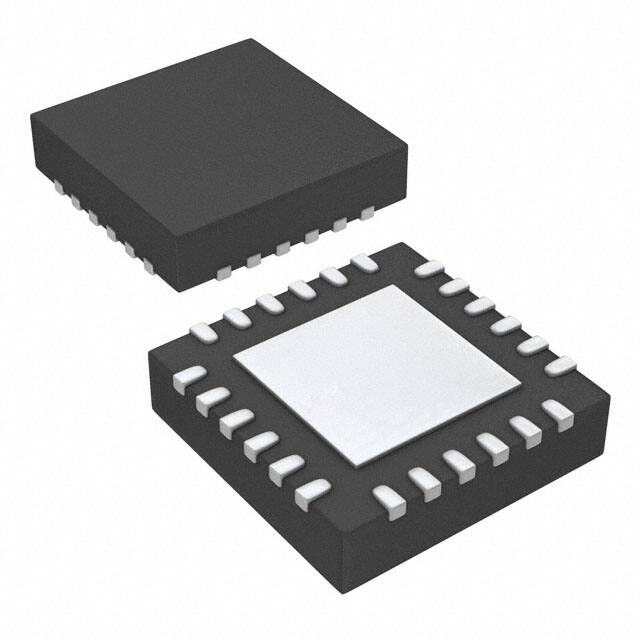


 工商网监
湘ICP备2023018690号
工商网监
湘ICP备2023018690号
