LM5150-Q1
SNVSAP6C – SEPTEMBER 2017 – REVISED OCTOBER 2021
LM5150-Q1 Wide VIN Automotive Low IQ Boost Controller
1 Features
3 Description
•
The LM5150-Q1 device is a wide input range
automatic boost controller. The device is suitable
for use as a pre-boost converter which maintains
the output voltage from a vehicle battery during
automotive cranking or from a back-up battery during
the loss of vehicle battery.
•
•
•
•
•
•
•
•
•
•
•
•
•
2 Applications
•
•
•
The LM5150-Q1 switching frequency is programmed
by a resistor from 220 kHz to 2.3 MHz. Fast switching
(≥ 2.2 MHz) minimizes AM band interference and
allows for a small solution size and fast transient
response.
The LM5150-Q1 operates in low IQ standby mode
when the input or output voltage is above the preset
standby thresholds and automatically wakes up when
the output voltage drops below the preset wake-up
threshold.
The device transients in and out of the low IQ standby
mode to extend battery life at light load. A single
resistor programs the target output regulation voltage
as well as the configuration. Additional features
include low shutdown current, boost status indicator,
adjustable cycle-by-cycle current limit, and thermal
shutdown.
Device Information
LM5150-Q1
(1)
Automotive start-stop system
Automotive emergency call system
Battery-powered boost converters
VSUPPLY
PACKAGE(1)
PART NUMBER
WQFN (16)
BODY SIZE (NOM)
4.00 mm × 4.00 mm
For all available packages, see the orderable addendum at
the end of the data sheet.
100
VLOAD
95
VIN
LO
CS
AGND
PGND
VOUT
EN
STATUS
Efficiency (%)
•
AEC-Q100 qualified:
– Device temperature grade 1: –40°C to +125°C
ambient operating temperature range
– Device HBM ESD classification level 2
– Device CDM ESD classification level C4B
Functional Safety-Capable
– Documentation available to aid functional safety
system design
Wide VIN input range from 1.5 V to 42 V when
VOUT ≥ 5 V (65-V absolute maximum)
Low shutdown current (IQ ≤ 5 µA)
Low standby current (IQ ≤ 15 µA)
Four programmable output voltage options and
two selectable configurations
– 6.8 V, 7.5 V, 8.5 V, or 10.5 V
– Start-stop or e-call configurations
Adjustable switching frequency from 220 kHz to
2.3 MHz
Automatic wake-up and standby mode transition
Optional clock synchronization
Boost status indicator
1.5-A peak MOSFET gate driver
Adjustable cycle-by-cycle current limit
Thermal shutdown
16-pin WQFN with wettable and non-wettable flank
options
Create a custom design using the LM5150-Q1 with
the WEBENCH® Power Designer
90
85
80
LM5150
VSUPPLY=5.5V
VSUPPLY=4.5V
VSUPPLY=3.5V
VSUPPLY=2.5V
COMP
SYNC
75
RT
VSET
VCC
AVCC
70
0
Typical Application Circuit
0.3
0.6
0.9
1.2 1.5 1.8
Load Current (A)
2.1
2.4
2.7
3
D008
Efficiency (VLOAD = 6.8 V, FSW = 440 kHz)
An IMPORTANT NOTICE at the end of this data sheet addresses availability, warranty, changes, use in safety-critical applications,
intellectual property matters and other important disclaimers. PRODUCTION DATA.
�LM5150-Q1
www.ti.com
SNVSAP6C – SEPTEMBER 2017 – REVISED OCTOBER 2021
Table of Contents
1 Features............................................................................1
2 Applications..................................................................... 1
3 Description.......................................................................1
4 Revision History.............................................................. 2
5 Device Comparison Table...............................................3
6 Pin Configuration and Functions...................................4
7 Specifications.................................................................. 6
7.1 Absolute Maximum Ratings........................................ 6
7.2 ESD Ratings............................................................... 6
7.3 Recommended Operating Conditions.........................6
7.4 Thermal Information....................................................7
7.5 Electrical Characteristics.............................................7
7.6 Typical Characteristics.............................................. 10
8 Detailed Description......................................................12
8.1 Overview................................................................... 12
8.2 Functional Block Diagram......................................... 12
8.3 Feature Description...................................................13
8.4 Device Functional Modes..........................................19
9 Application and Implementation.................................. 23
9.1 Application Information............................................. 23
9.2 Typical Application.................................................... 26
9.3 System Examples..................................................... 34
10 Power Supply Recommendations..............................36
11 Layout........................................................................... 37
11.1 Layout Guidelines................................................... 37
11.2 Layout Example...................................................... 38
12 Device and Documentation Support..........................39
12.1 Device Support....................................................... 39
12.2 Receiving Notification of Documentation Updates..39
12.3 Support Resources................................................. 39
12.4 Trademarks............................................................. 39
12.5 Electrostatic Discharge Caution..............................39
12.6 Glossary..................................................................39
13 Mechanical, Packaging, and Orderable
Information.................................................................... 40
4 Revision History
NOTE: Page numbers for previous revisions may differ from page numbers in the current version.
Changes from Revision B (June 2020) to Revision C (October 2021)
Page
• Added non-wettable flank options ......................................................................................................................1
• Updated the numbering format for tables, figures, and cross-references throughout the document. ................1
• Added Section 5 ................................................................................................................................................ 3
Changes from Revision A (February 2020) to Revision B (June 2020)
Page
• Added functional safety bullet to Section 1 ........................................................................................................1
2
Submit Document Feedback
Copyright © 2021 Texas Instruments Incorporated
Product Folder Links: LM5150-Q1
�LM5150-Q1
www.ti.com
SNVSAP6C – SEPTEMBER 2017 – REVISED OCTOBER 2021
5 Device Comparison Table
PART NUMBER
LM5150QRUMRQ1
LM5150QRUMTQ1
LM5150QURUMRQ1
PACKAGE OUTLINE
WETTABLE (WF)/NON-WETTABLE
FLANKS (NON-WF)
RUM0016C
WF
RUM0016F
Non-WF
Submit Document Feedback
Copyright © 2021 Texas Instruments Incorporated
Product Folder Links: LM5150-Q1
3
�LM5150-Q1
www.ti.com
SNVSAP6C – SEPTEMBER 2017 – REVISED OCTOBER 2021
SYNC
1
STATUS
2
VSET
RT
COMP
AP
VIN
6 Pin Configuration and Functions
16
15
14
13
AP
12
CS
11
AGND
EP
VOUT
4
9
LO
AP
5
6
7
8
NC
PGND
AVCC
10
NC
3
PVCC
EN
AP
Figure 6-1. 16-Pin WQFN RUM Package (Top View)
Table 6-1. Pin Functions
PIN
4
I/O(1)
DESCRIPTION
NO.
NAME
1
SYNC
I
External synchronization clock input pin. The internal oscillator is synchronized to an
external clock by applying a pulse signal into the SYNC pin in the start-stop configuration.
Connect directly to ground if not used or in emergency call configuration. Maximum duty
cycle limit can be programmed by controlling the external synchronization clock frequency.
2
STATUS
O
Status indicator with an open-drain output stage. Internal pulldown switch holds the pin low
when the device is not boosting. The pin can be left floating if not used.
3
EN
I
Enable pin. If EN is below 1 V, the device is in shutdown mode. The pin must be raised
above 2 V to enable the device. Connect directly to VOUT pin for an automatic boost.
4
VOUT
I/P
Boost output voltage-sensing pin and input to VCC regulator. Connect to the output of the
boost converter.
5
PVCC
O/P
Output of the VCC bias regulator. Decouple locally to PGND using a low-ESR or low-ESL
ceramic capacitor located as close to the device as possible.
6
NC
—
No internal electrical connection. Leave the pin floating or connect directly to ground.
7
AVCC
I/P
Analog VCC supply input. Decouple locally to AGND using 0.1-µF low-ESR or low-ESL
ceramic capacitor located as close to the device as possible. Connect to the PVCC pin
through 10-Ω resistor.
8
NC
—
No internal electrical connection. Leave the pin floating or connect directly to ground.
9
LO
O
N-channel MOSFET gate drive output. Connect to the gate of the N-channel MOSFET
through a short, low inductance path.
10
PGND
G
Power ground pin. Connect to the ground connection of the sense resistor through a wide
and short path.
11
AGND
G
Analog ground pin. Connect to the analog ground plane through a wide and short path.
12
CS
I
Current sense input pin. Connect to the positive side of the current sense resistor through a
short path.
13
COMP
O
Output of the internal transconductance error amplifier. The loop compensation components
must be connected between this pin and AGND.
14
RT
I
Switching frequency setting pin. The switching frequency is programmed by a single resistor
between RT and AGND.
15
VSET
I
Configuration selection and VOUT regulation target programming pin. During initial power
on, a resistor between the VSET pin and AGND configures the VOUT regulation target and
the configuration.
Submit Document Feedback
Copyright © 2021 Texas Instruments Incorporated
Product Folder Links: LM5150-Q1
�LM5150-Q1
www.ti.com
SNVSAP6C – SEPTEMBER 2017 – REVISED OCTOBER 2021
Table 6-1. Pin Functions (continued)
PIN
NO.
NAME
I/O(1)
16
VIN
I
—
EP
—
—
—
AP
(1)
DESCRIPTION
Boost input voltage sensing pin. Connect to the input supply of the boost converter.
Exposed pad of the package. No internal electrical connection to silicon die. The EP is
electrically connected to anchor pads. The EP must be connected to the large ground
copper plain to reduce thermal resistance.
Anchor pad of the package. No internal electrical connection to silicon die. The AP is
electrically connected to the EP. The AP can be left floating or soldered to the ground
copper.
G = Ground, I = Input, O = Output, P = Power
Submit Document Feedback
Copyright © 2021 Texas Instruments Incorporated
Product Folder Links: LM5150-Q1
5
�LM5150-Q1
www.ti.com
SNVSAP6C – SEPTEMBER 2017 – REVISED OCTOBER 2021
7 Specifications
7.1 Absolute Maximum Ratings
Over the recommended operating junction temperature range of –40°C to 150°C (unless otherwise noted)(1)
MIN
MAX
VIN to AGND
–0.3
65
VOUT to AGND
–0.3
65
EN to AGND
–0.3
65
RT to
Input
Output
AGND(2)
UNIT
–0.3
AVCC + 0.3
SYNC to AGND
–0.3
7
VSET to AGND
–0.3
7
CS to AGND (DC)
–0.3
AVCC + 0.3
CS to AGND (40-ns transient)
–1.0
AVCC + 0.3
CS to AGND (20-ns transient)
–2.0
AVCC + 0.3
PGND to AGND
–0.3
0.3
LO to AGND (DC)
–0.3
PVCC + 0.3
LO to AGND (40-ns transient)
–1.0
PVCC + 0.3
LO to AGND (20-ns transient)
–2.0
PVCC + 0.3
STATUS to AGND(3)
–0.3
65
COMP to
AGND(2)
V
V
–0.3
AVCC + 0.3
AVCC to AGND
–0.3
7
PVCC to AVCC
–0.3
0.3
TJ
Junction temperature(4)
–40
150
℃
Tstg
Storage temperature
–55
150
℃
(1)
(2)
(3)
(4)
Stresses beyond those listed under Absolute Maximum Ratings may cause permanent damage to the device. These are stress
ratings only, which do not imply functional operation of the device at these or any other conditions beyond those indicated
underRecommended Operating Conditions. Exposure to absolute-maximum-rated conditions for extended periods may affect device
reliability.
The pin voltage is clamped by an internal circuit, and is not specified to have an external voltage applied.
STATUS can go below ground during the STATUS low-to-high transition. The negative voltage on STATUS during this transition is
clamped by an internal diode and it does not damage the device.
High junction temperatures degrade operating lifetimes. Operating lifetime is de-rated for junction temperatures greater than 125°C.
7.2 ESD Ratings
Human body model (HBM), per AEC
V(ESD)
(1)
Electrostatic discharge
Charged device model
(CDM), per AEC Q100-011
Q100-002(1)
MIN
MAX
–2000
2000
Corner pins
–750
750
Other pins
–500
500
UNIT
V
AEC Q100-002 indicates HBM stressing is done in accordance with the ANSI/ESDA/JEDEC JS-001 specification.
7.3 Recommended Operating Conditions
Over the recommended operating junction temperature range of –40°C to 150°C (unless otherwise specified)(1)
MIN
VVIN
6
Boost input voltage sense
VVOUT
Boost output voltage
VEN
EN input
sense(2)
voltage(3)
VPVCC
PVCC
VSYNC
SYNC input
VCS
Current sense input
FSW
Typical switching frequency
MAX
UNIT
42
V
5
42
V
0
42
V
5.5
V
5.5
V
4.5
0
Submit Document Feedback
NOM
1.5
5
0
0.3
220
2300
V
kHz
Copyright © 2021 Texas Instruments Incorporated
Product Folder Links: LM5150-Q1
�LM5150-Q1
www.ti.com
SNVSAP6C – SEPTEMBER 2017 – REVISED OCTOBER 2021
Over the recommended operating junction temperature range of –40°C to 150°C (unless otherwise specified)(1)
MIN
FSYNC
TJ
(1)
(2)
(3)
(4)
MAX
UNIT
Synchronization pulse frequency
220
2300
kHz
temperature(4)
–40
150
°C
Operating junction
NOM
Operating Ratings are conditions under the device is intended to be functional. For specifications and test conditions, see Electrical
Characteristics.
The device requires minimum 5V at VOUT pin to start up
VPVCC should be less than VVOUT + 0.3 V
High junction temperatures degrade operating lifetimes. Operating lifetime is derated for junction temperatures greater than 125°C.
7.4 Thermal Information
LM5150-Q1
THERMAL METRIC(1)
RUM (WQFN)
UNIT
16 PINS
RθJA
Junction-to-ambient thermal resistance
44.4
°C/W
RθJC(top)
Junction-to-case (top) thermal resistance
33.4
°C/W
RθJB
Junction-to-board thermal resistance
19.5
°C/W
ΨJT
Junction-to-top characterization parameter
0.5
°C/W
ΨJB
Junction-to-board characterization parameter
19.3
°C/W
RθJC(bot)
Junction-to-case (bottom) thermal resistance
2
°C/W
(1)
For more information about traditional and new thermal metrics, see the Semiconductor and IC Package Thermal Metrics application
report.
7.5 Electrical Characteristics
Typical values correspond to TJ = 25°C. Minimum and maximum limits apply over TJ = –40°C to 125°C. Unless otherwise
stated, VVOUT = 6.8 V, RT = 9.09 kΩ
PARAMETER
TEST CONDITIONS
MIN
TYP
MAX UNIT
SUPPLY CURRENT
ISHUTDOWN(VOUT)
VOUT shutdown current
VVOUT = 12 V, VEN = 0 V
5
12
µA
ISTANDBY(VOUT)
VOUT standby current (PVCC in
regulation, STATUS is low)
VVOUT = 12 V, VEN = 3.3 V, RSET =
90.9 kΩ
15
25
µA
IWAKEUP(VOUT)
VOUT operating current (exclude
current into RT resistor)
VVOUT = 10.5 V, VEN = 2.5 V, nonswitching, RT = 9.09 kΩ
1.2
2.0
mA
ISHUTDOWN(VIN)
VIN shutdown current
VVIN = 12 V, VEN = 0 V
0.1
0.5
µA
ISTANDBY(VIN)
VIN standby current
VVIN = 12 V, VEN = 3.3 V, RSET = 29.4
kΩ
0.1
0.5
µA
IWAKEUP(VIN)
VIN operating current
VVIN = 10.5 V, VEN = 2.5 V, nonswitching, RT = 9.09 kΩ
30
45
µA
VVCC-REG-NOLOAD
PVCC regulation
VVOUT = 6.0 V, No load, wake-up mode
4.75
5
5.25
V
VVCC-REG-FULLLOAD
PVCC regulation
VVOUT = 5.0 V, IPVCC = 70 mA
4.5
4.8
VVCC-UVLO-RISING
AVCC UVLO threshold
AVCC rising
4.1
4.3
4.5
V
VVCC-UVLO-FALLING
AVCC UVLO threshold
AVCC falling
3.9
4.1
4.3
V
VVCC-UVLO-HYS
AVCC UVLO hysteresis
IVCC-CL
PVCC sourcing current limit
VPVCC = 0 V, wake-up mode
75
VEN-RISING
Enable threshold
EN rising
VEN-FALLING
Enable threshold
EN falling
IEN
EN bias current
VEN = 42 V
VCC REGULATOR
V
0.2
V
mA
ENABLE
1.7
1
2
V
100
nA
1.3
V
6.8-V SETTING
Submit Document Feedback
Copyright © 2021 Texas Instruments Incorporated
Product Folder Links: LM5150-Q1
7
�LM5150-Q1
www.ti.com
SNVSAP6C – SEPTEMBER 2017 – REVISED OCTOBER 2021
Typical values correspond to TJ = 25°C. Minimum and maximum limits apply over TJ = –40°C to 125°C. Unless otherwise
stated, VVOUT = 6.8 V, RT = 9.09 kΩ
PARAMETER
TEST CONDITIONS
MIN
TYP
MAX UNIT
VVOUT-REG
VOUT regulation target
RSET = 29.4 kΩ or 90.9 kΩ
6.66
6.80
6.98
V
VVOUT-WAKEUP
VOUT wake-up threshold
(VVOUT-REG + 3%)
RSET = 29.4 kΩ or 90.9 kΩ, VOUT
falling
6.83
7.00
7.14
V
VVOUT-STANDBY1
VOUT standby threshold
(VVOUT-REG + 6%, EC config)
RSET = 90.9 kΩ, VOUT rising
7.02
7.21
7.35
V
VVOUT-STATUS-OFF
VOUT status off threshold
(VVOUT-REG + 12%, EC config)
RSET = 90.9 kΩ, VOUT rising
7.42
7.62
7.81
V
VVOUT-STANDBY2
VOUT standby threshold
(VVOUT-REG + 24%, SS config)
RSET = 29.4 kΩ, VOUT rising
8.22
8.43
8.60
V
VVIN-STANDBY
VIN standby threshold
(VVOUT-WAKEUP + 1.0 V, SS config)
RSET = 29.4 kΩ, VIN rising
7.82
8.00
8.19
V
VVOUT-REG
VOUT regulation target
RSET = 19.1 kΩ or 71.5 kΩ
7.37
7.50
7.67
V
VVOUT-WAKEUP
VOUT wake-up threshold
(VVOUT-REG + 3%)
RSET = 19.1 kΩ or 71.5 kΩ, VOUT
falling
7.52
7.73
7.88
V
VVOUT-STANDBY1
VOUT standby threshold
(VVOUT-REG + 6%, EC config)
RSET = 71.5 kΩ, VOUT rising
7.74
7.95
8.11
V
VVOUT-STATUS-OFF
VOUT status off threshold
(VVOUT-REG + 12%, EC config)
RSET = 71.5 kΩ, VOUT rising
8.19
8.40
8.61
V
VVOUT-STANDBY2
VOUT standby threshold
(VVOUT-REG + 24%, SS config)
RSET = 19.1 kΩ, VOUT rising
9.07
9.30
9.46
V
VVIN-STANDBY
VIN standby threshold
(VVOUT-WAKEUP + 1.0 V, SS config)
RSET = 19.1 kΩ, VIN rising
8.50
8.73
8.93
V
VVOUT-REG
VOUT regulation target
RSET = 9.53 kΩ or 54.9 kΩ
8.37
8.50
8.69
V
VVOUT-WAKEUP
VOUT wake-up threshold
(VVOUT-REG + 3%)
RSET = 9.53 kΩ or 54.9 kΩ, VOUT
falling
8.52
8.76
8.93
V
VVOUT-STANDBY1
VOUT standby threshold
(VVOUT-REG + 6%, EC config)
RSET = 54.9 kΩ, VOUT rising
8.78
9.01
9.19
V
VVOUT-STATUS-OFF
VOUT status off threshold
(VVOUT-REG + 12%, EC config)
RSET = 54.9 kΩ, VOUT rising
9.28
9.52
9.75
V
VVOUT-STANDBY2
VOUT standby threshold
(VVOUT-REG + 24%, SS config)
RSET = 9.53 kΩ, VOUT rising
10.29
10.54
10.72
V
VVIN-STANDBY
VIN standby threshold
(VVOUT-WAKEUP + 1.0 V, SS config)
RSET = 9.53 kΩ, VIN rising
9.50
9.76
9.98
V
VVOUT-REG
VOUT regulation target
RSET = GND or 41.2 kΩ
10.31
10.50
10.75
V
VVOUT-WAKEUP
VOUT wake-up threshold
(VVOUT-REG + 3%)
RSET = GND or 41.2 kΩ, VOUT falling
10.53
10.82
11.02
V
VVOUT-STANDBY1
VOUT standby threshold
(VVOUT-REG + 6%, EC config)
RSET = 41.2 kΩ, VOUT rising
10.84
11.13
11.33
V
VVOUT-STATUS-OFF
VOUT status off threshold
(VVOUT-REG + 12%, EC config)
RSET = 41.2 kΩ, VOUT rising
11.46
11.76
12.04
V
VVOUT-STANDBY2
VOUT standby threshold
(VVOUT-REG + 24%, SS config)
RSET = GND, VOUT rising
12.70
13.02
13.24
V
VVIN-STANDBY
VIN standby threshold
(VVOUT-WAKEUP + 1.0 V, SS config)
RSET = GND, VIN rising
11.47
11.82
12.11
V
7.5-V SETTING
8.5-V SETTING
10.5-V SETTING
RT
VRT-REG
RT regulation voltage
1.2
V
CLOCK SYNCHRONIZATION
VSYNC-RISING
8
SYNC rising threshold
2.0
Submit Document Feedback
2.4
V
Copyright © 2021 Texas Instruments Incorporated
Product Folder Links: LM5150-Q1
�LM5150-Q1
www.ti.com
SNVSAP6C – SEPTEMBER 2017 – REVISED OCTOBER 2021
Typical values correspond to TJ = 25°C. Minimum and maximum limits apply over TJ = –40°C to 125°C. Unless otherwise
stated, VVOUT = 6.8 V, RT = 9.09 kΩ
PARAMETER
VSYNC-FALLING
TEST CONDITIONS
SYNC falling threshold
MIN
TYP
0.4
1.5
MAX UNIT
V
PULSE WIDTH MODULATION AND OSCILLATOR
FSW1
Switching frequency
RT = 93.1 kΩ
204
239
270
kHz
FSW2
Switching frequency
RT = 9.09 kΩ
2100
2300
2500
kHz
FSW3
Switching frequency
RT = 9.09 kΩ,
FSYNC = 2.0 MHz
TON-MIN
Forced minimum on time
SS config, VCOMP = 0 V
DMIN
Minimum duty cycle limit (EC config)
DMAX
Maximum duty cycle limit
2000
30
50
RT = 9.09 kΩ, VVIN = 1.5 V, VVOUT =
6.8 V, VCOMP = 0 V
60%
RT = 93.1 kΩ, VVIN = 8.4 V, VVOUT =
10.5 V, VCOMP = 0 V
16%
kHz
70
SS config, RT = 9.09 kΩ
83%
87% 91.5%
EC config, RT = 93.1 kΩ
83%
87% 91.5%
ns
CURRENT SENSE
VCSTH
Current limit threshold
(CS-AGND)(1)
VVIN = 5.1 V, VVOUT = 6.8 V at 25% DC
102
120
138
mV
VVIN = 3.4 V, VVOUT = 6.8 V at 50% DC
102
120
138
mV
VVIN = 1.7 V, VVOUT = 6.8 V at 75% DC
102
120
138
mV
ERROR AMPLIFIER
Gm
Transconductance
2
mA/V
COMP souring current
VCOMP = 0 V
312
µA
COMP sinking current
VCOMP = 1.5 V
120
µA
COMP clamp voltage
2.4
COMP to PWM offset
2.6
V
0.3
V
0.1
V
STATUS
Low-state voltage drop
1-mA sinking
STATUS rise to LO delay
5-kΩ pullup to 5 V
High-state voltage drop
50-mA sinking
0.075
V
Low-state voltage drop
50-mA sourcing
0.055
V
175
°C
15
°C
4
5
6
µs
MOSFET DRIVER
THERMAL SHUTDOWN (TSD)
Thermal shutdown threshold
Temperature rising
Thermal shutdown hysteresis
(1)
VCL at the current limit comparator input is 10 x VCSTH
Submit Document Feedback
Copyright © 2021 Texas Instruments Incorporated
Product Folder Links: LM5150-Q1
9
�LM5150-Q1
www.ti.com
SNVSAP6C – SEPTEMBER 2017 – REVISED OCTOBER 2021
7.6 Typical Characteristics
126
17
Peak Current in Current Limit (A)
16.5
16
Current Limit Threshold at CS (mV)
6.8V output
7.5V output
8.5V output
10.5V output
15.5
15
14.5
14
13.5
13
2
3
4
5
6
7
Supply Voltage (V)
8
9
6.8V output
7.5V output
8.5V output
10.5V output
124
122
120
118
116
114
20
10
30
40
D001
Figure 7-1. Peak Inductor Current vs Supply
Voltage (FSW = 250 kHz, RS = 8 mΩ)
50
60
Duty Cycle (%)
70
80
D002
Figure 7-2. Current Limit Threshold at CS vs Duty
Cycle
6
6
5.5
5
5
4.5
4
VPVCC (V)
VPVCC (V)
4
3
3.5
3
2.5
2
2
1.5
1
1
0.5
0
0
0
20
40
60
80
IPVCC (mA)
100
120
1
1.5
2
2.5 3 3.5
VVOUT (V)
4
4.5
5
5.5
6
D004
Figure 7-4. VPVCC vs VVOUT (EN = 3.3 V, IPVCC = 10
mA, VOUT Rising)
100
2500
90
Duty Cycle Limit in EC mode (%)
2750
2250
2000
Frequency (kHz)
0.5
D003
Figure 7-3. VPVCC vs IPVCC (VOUT = 6 V)
1750
1500
1250
1000
750
500
250
VVOUT=6.8V
VVOUT=7.5V
VVOUT=8.5V
VVOUT=10.5V
80
70
60
50
40
30
20
10
0
0
10
20
30
40
50
60
RT (k:)
70
80
90
100
0
0
1
D005
Figure 7-5. Frequency vs RT
10
0
140
2
3
4
5
6
7
VVIN (V)
8
9
10
11
12
D006
Figure 7-6. Duty Cycle Limit in EC Configuration vs
VVIN
Submit Document Feedback
Copyright © 2021 Texas Instruments Incorporated
Product Folder Links: LM5150-Q1
�LM5150-Q1
www.ti.com
SNVSAP6C – SEPTEMBER 2017 – REVISED OCTOBER 2021
100
20
18
95
16
Efficiency (%)
IVOUT (uA)
14
Shutdown
Standby
12
10
8
6
4
90
85
80
VSUPPLY=5.5V
VSUPPLY=4.5V
VSUPPLY=3.5V
VSUPPLY=2.5V
75
2
0
-60
70
-40
-20
0
20 40 60 80
Temperature (°C)
100 120 140 160
0
0.3
D007
Figure 7-7. IVOUT vs Temperature
0.6
0.9
1.2 1.5 1.8
Load Current (A)
2.1
2.4
2.7
3
D008
Figure 7-8. Efficiency vs Load Current (VLOAD = 6.8
V, FSW = 440 kHz, SS Configuration)
Submit Document Feedback
Copyright © 2021 Texas Instruments Incorporated
Product Folder Links: LM5150-Q1
11
�LM5150-Q1
www.ti.com
SNVSAP6C – SEPTEMBER 2017 – REVISED OCTOBER 2021
8 Detailed Description
8.1 Overview
The LM5150-Q1 device is a wide input range automotive boost controller designed for automotive start-stop
or emergency-call applications. The device can maintain the output voltage from a vehicle battery during
automotive cranking or from a back-up battery during the loss of vehicle battery. The wide input range of the
device covers automotive load dump transient. The control method is based upon peak current mode control.
To extend the battery life time, the LM5150-Q1 features a low IQ standby mode with automatic wake-up and
standby control. The device stays in low IQ standby mode when the boost operation is not required, and
automatically enters wake-up mode when the output voltage drops below the preset wake-up threshold. High
value feedback resistors are included inside the device to minimize leakage current in the low IQ standby mode.
The LM5150-Q1 operates in one of two selectable configurations when waking up. In Start-Stop configuration
(SS configuration), the device runs at a fixed switching frequency without any pulse skipping until it enters
standby mode, which helps to have a fixed EMI spectrum. In Emergency-Call configuration (EC configuration),
the device will skip pulses as it automatically alternates between low IQ standby mode and wake-up mode to
extend the battery life in light load conditions.
The LM5150-Q1 switching frequency is programmable from 220 kHz to 2.3 MHz. Fast switching (≥ 2.2 MHz)
minimizes AM band interference and allows for a small solution size and fast transient response. A single
resistor at the VSET pin programs the target output regulation voltage as well as the configuration. This
eliminates the need for an external feedback resistor divider which enables low IQ operation. The device also
features clock synchronization in the SS configuration, low quiescent current in shutdown mode, a boost status
indicator, adjustable cycle-by-cycle current will limit, and thermal shutdown protection.
8.2 Functional Block Diagram
VSUPPLY
D1
VLOAD
LM
COUT
CIN
RLOAD
STATUS
VIN
(SS Mode)
VIN_STANDBY
StatusB
VSET
Standby
RSET
S
Q
R
Q
S
±
REF
+
Wakeup
FB
VOUT
±
VO_WAKE
REF
+
(EC Mode)
VO_STATUS_OFF
StatusB
VOUT
±
R
Q
+
VIN_STANDBY (SS Mode)
2.0 V/1.0 V
AVCC
REF
CAVCC
+
VOUT
Enable
±
EN
VOUT-STANDBY
±
VO_STANDBY
VSET
Ready
POWER
ON
VOLTAGE
SELECT
Q
+
PVCC
Ready
VCC_OK
LM5150
TSD
VOUT
VCL + 0.3 V
±
VCC
Regulator
Enable
Standby
VCC_OK
C/L
+
S
Q
R
Q
RAVCC
CPVCC
VCC
UVLO
LO
VCS_OFFSET
Wakeup
+
ISLOPE
±
±
VCS
VCS_OFFSET
+
PGND
AGND
30 uA peak
DMAX/Forced_Toff
CLOCK
GENERATOR
GM AMP
COMP
RCOMP
Q1
DMIN/Forced_Ton
C/L
+
RT
SYNC
±
FB
REF
PWM
+
A = 10
±
CS
RSL
(optional)
RF
2k
TLEB
CF
RS
0.3 V
RT
CCOMP
12
Submit Document Feedback
Copyright © 2021 Texas Instruments Incorporated
Product Folder Links: LM5150-Q1
�LM5150-Q1
www.ti.com
SNVSAP6C – SEPTEMBER 2017 – REVISED OCTOBER 2021
8.3 Feature Description
8.3.1 Enable (EN Pin)
When the EN pin voltage is less than 1 V, the LM5150-Q1 is in shutdown mode with all other functions disabled.
To turn on the internal VCC regulator and begin start-up sequence, the EN pin voltage must be greater than 2 V.
If the EN pin is controlled by user input, it is recommended to supply a voltage greater than 3 V at the EN pin. If
the EN pin is not controlled by user input, connect the EN pin to the VOUT pin directly. See Section 8.4 for more
detailed information.
8.3.2 High Voltage VCC Regulator (PVCC, AVCC Pin)
The LM5150-Q1 contains an internal high voltage VCC regulator. The VCC regulator turns on when the EN pin
voltage is greater than 2 V. The VCC regulator is sourced from the VOUT pin and provides 5 V (typical) bias
supply for the N-channel MOSFET driver and other internal circuits.
The VCC regulator sources current into the capacitor connected to the PVCC pin with a minimum of 75-mA
capability when the LM5150-Q1 is in the wake-up mode and during the device configuration period. The
maximum sourcing capability is decreased to 17 mA in standby mode. The recommended PVCC capacitor
is 4.7 µF to 10 µF. In normal operation, the PVCC pin voltage is either 5 V or VVOUT + 0.3 V, whichever is lower.
The AVCC pin is the analog bias supply input of the LM5150-Q1. The recommended AVCC capacitor is 0.1-μF.
Connect to the PVCC pin through 10-Ω resistor.
8.3.3 Power-On Voltage Selection (VSET Pin)
During initial power on, the VOUT regulation target and the configuration are configured by a resistor connected
between the VSET and the AGND pins. The configuration starts when the EN pin voltage is greater than 2 V
and the AVCC voltage crosses the AVCC UVLO threshold, and requires typically 50 µs to finish. To reset and
reconfigure, EN should be toggled below 1 V or AVCC/VOUT must be fully discharged.
EN
Wake-up or standby
Configuration
AVCC
Shutdown
Configuration
Shutdown
Wake-up or standby
VCC
UVLO
50 us
50 us
Figure 8-1. Power-On Voltage Selection
The VOUT regulation target can be programmed to 6.8 V, 7.5 V, 8.5 V, or 10.5 V with the appropriate resistor
with 5% tolerance. The configuration can be selected as either SS or EC configuration. The LM5150-Q1 will not
switch during the 50-µs configuration time.
Table 8-1. VSET Resistors(1)
CONFIGURATION
(1)
EMERGENCY-CALL
START-STOP
VOUT regulation target
6.8 V
7.5 V
8.5 V
10.5 V
6.8 V
7.5 V
8.5 V
10.5 V
RSET [Ω]
90.9 k
71.5 k
54.9 k
41.2 k
29.4 k
19.1 k
9.53 k
Ground
If other output regulation targets are required, contact the sales office/distributors for availability.
Submit Document Feedback
Copyright © 2021 Texas Instruments Incorporated
Product Folder Links: LM5150-Q1
13
�LM5150-Q1
SNVSAP6C – SEPTEMBER 2017 – REVISED OCTOBER 2021
www.ti.com
8.3.4 Switching Frequency (RT Pin)
The switching frequency of the LM5150-Q1 is set by a single RT resistor connected between the RT and the
AGND pins. The resistor value to set the switching frequency (FSW) is calculated using Equation 1.
RT
2.233 u 1010
FSW _ RT
619 :
TYPICAL
(1)
The RT pin is regulated to 1.2 V by the internal RT regulator during wake-up.
8.3.5 Clock Synchronization (SYNC Pin in SS Configuration)
In SS configuration, the switching frequency of the LM5150-Q1 can be synchronized to an external clock by
directly applying a pulse signal to the SYNC pin. The internal clock of the LM5150-Q1 is synchronized at the
rising edge of the external clock. The device ignores the rising edge input during forced off-time.
The external synchronization pulse must be greater than the 2.4 V in the high logic state and must be less than
0.4 V in the low logic state. The duty cycle of the external synchronization pulse is not limited, but the minimum
pulse width should be greater than 100 ns. Because the maximum duty cycle limit and the peak current limit
threshold are affected by synchronizing the switching frequency to an external synchronization pulse, take extra
care when using the clock synchronization function. See Section 8.3.11 and Section 8.3.7 for more detailed
information.
If the minimum input supply voltage of the boost converter is greater than ¼ of the VOUT regulation target
(VVOUT-REG), the frequency of the external synchronization pulse (FSYNC) should be within +15% and –15% of
the typical free-running switching frequency (FSW(TYPICAL))
0.85 ´ FSW_RT(TYPICAL) £ FSYNC £ 1.15 ´ FSW_RT(TYPICAL)
(2)
In this range, a maximum 1:4 (VSUPPLY:VLOAD) step-up ratio is allowed.
A higher step-up ratio can be achieved by supplying a lower frequency synchronization pulse. 1:5 step-up ratio
can be achieved by selecting FSYNC within –25% and –15% of the FSW_RT(TYPICAL).
0.75 ´ FSW_RT(TYPICAL) £ FSYNC £ 0.85 ´ FSW_RT(TYPICAL)
(3)
In this range, a maximum 1:5 (VSUPPLY:VLOAD) step-up ratio is allowed.
8.3.6 Current Sense, Slope Compensation, and PWM (CS Pin)
The LM5150-Q1 features a low-side current sense amplifier with a gain of 10, and provides an internal slope
compensation ramp to prevent subharmonic oscillation at high duty cycle. The device generates the slope
compensation ramp using a sawtooth current source with a slope of 30 µA × FSW (typical). This current flows
through an internal 2-kΩ resistor and out of the CS pin. The slope compensation ramp is determined by the RT
resistor and is 60 mV × FSW (typical) at the input of the current sense amplifier and 600 mV × FSW (typical)
at the output of the current sense amplifier. The slope compensation ramp can be increased by adding an
external slope resistor (RSL) between the sense resistor (RS) and the CS pin, but take extra care when using
RSL, because the peak current limit is affected by adding RSL. See Section 8.3.7 for more detailed information.
14
Submit Document Feedback
Copyright © 2021 Texas Instruments Incorporated
Product Folder Links: LM5150-Q1
�LM5150-Q1
www.ti.com
SNVSAP6C – SEPTEMBER 2017 – REVISED OCTOBER 2021
Current Limit
Q1
±
VCL +0.3 V
30 uA peak
+
ISLOPE
+
+
PWM
±
±
2k
CS
RSL
(optional)
RF
+
A = 10
±
CF
0.3 V
RS
COMP
Figure 8-2. Current Sensing and Slope Compensation
According to peak current mode control theory, the slope of the compensation ramp must be greater than half
of the sensed inductor current falling slope to prevent subharmonic oscillation at high duty cycle. Therefore, the
minimum amount of slope compensation should satisfy the following inequality:
0.5 ´
(VLOAD + VF ) - VSUPPLY
× RS × Margin < 30mA ´ (2kΩ + RSL )× FSW
LM
(4)
VF is a forward voltage drop of D1, the external diode. 1.2 is recommended as a margin to cover non-ideal
factors.
If required, RSL can be added to increase the slope of the compensation ramp from half to 82% of the slope of
the sensed inductor current during the falling slope. The typical RSL value is calculated using Equation 5. The
maximum RSL value is 1 kΩ
0.82 ´
(VLOAD + VF ) - VSUPPLY
× RS = 30mA ´ (2kΩ + RSL )× FSW
LM
(5)
The PWM comparator in Figure 8-2 compares the sum of sensed inductor current, the slope compensation
ramp, and a 0.3-V (typical) internal COMP-to-PWM offset with the COMP pin voltage (VCOMP), and terminates
the present cycle if the sum is greater than VCOMP.
8.3.7 Current Limit (CS Pin)
The LM5150-Q1 features cycle-by-cycle peak current limit without subharmonic oscillation at high duty cycle. If
the sum of the sensed inductor current and the slope compensation ramp exceeds the current limit threshold at
the current limit comparator input (VCL), the current limit comparator immediately terminates the present cycle.
To minimize the peak current limit variation due to changes in either the supply voltage or the output voltage, the
device features a variable current limit threshold which is calculated using Equation 6.
VCL = 1.2 + 0.6 ×
(VVOUT - VVIN )
[V]
VVOUT-REG
(6)
Cycle-by-cycle peak inductor current limit (IPEAK-CL) in steady state calculated as follows:
VCL - 10 ´ 30mA ´ (2kW + RSL ) ´
IPEAK -CL =
FSW_RT
FSYNC
´D
10 ´ RS
(7)
Submit Document Feedback
Copyright © 2021 Texas Instruments Incorporated
Product Folder Links: LM5150-Q1
15
�LM5150-Q1
www.ti.com
SNVSAP6C – SEPTEMBER 2017 – REVISED OCTOBER 2021
D = 1-
VSUPPLY
VLOAD +VF
(8)
FSYNC is included in the equation because the peak amplitude of the slope compensation varies with the
frequency of the external synchronization clock. Substitute FSW_RT for FSYNC if clock synchronization is not used.
Boost converters have a natural pass-through path from the supply to the load through the high-side power
diode (D1). Due to this path, boost converters cannot provide current limit protection when the output voltage is
close to or less than the input supply voltage.
A small external RC filter (RF, CF) at the CS pin is required to overcome the leading edge spike of the current
sense signal. Select an RF value which is greater than 30 Ω and a CF value which is greater than 1 nF. Due to
the effect of the filter, the peak current limit is not valid when the on-time is less than 2 × RF × CF.
8.3.8 Feedback and Error Amplifier (COMP Pin)
The LM5150-Q1 includes internal feedback resistors which are set based on the VSET pin resistor selection.
These feedback resistors are disconnected from the VOUT pin in standby mode to minimize quiescent current.
The feedback resistor divider is connected to an internal transconductance error amplifier which features high
output resistance (RO = 10 MΩ) and wide bandwidth (BW = 3 MHz). The internal transconductance error
amplifier sources current which is proportional to the difference between the feedback resistor divider voltage
and the internal reference. The output of the error amplifier is connected to the COMP pin, allowing the use of a
Type 2 loop compensation network.
RCOMP, CCOMP and optional CHF loop compensation components configure the error amplifier gain and phase
characteristics to achieve a stable loop response. This compensation network creates a pole at very low
frequency (FDP), a mid-band zero (FZ_EA), and a high frequency pole (FP_EA). See Section 9.2.2.8 for more
detailed information.
8.3.9 Automatic Wake-Up and Standby
The LM5150-Q1 wakes up when VVOUT drops below the VOUT wake-up threshold. The device goes into
standby when VVOUT rises above the VOUT standby threshold in EC or SS configuration or when VVIN rises
above the VIN standby threshold in SS configuration. The VOUT wake-up threshold is typically 3% higher than
the VOUT regulation target. The STATUS output is released in 3 µs (with a 50-kΩ pullup resistor to 5 V) after the
wake-up event. The LO driver is enabled 6 µs after the STATUS output starts rising.
VOUT
VIN
WAKEUP
+
+
VVOUT-STANDBY
REF
VIN_STANDBY
(SS Config)
Standby
Wakeup
FB
Q
S
Q
R
VO_STANDBY
VOUT
VO_WAKE
+
REF
Figure 8-3. Automatic Wake-Up and Standby Control
16
Submit Document Feedback
Copyright © 2021 Texas Instruments Incorporated
Product Folder Links: LM5150-Q1
�LM5150-Q1
www.ti.com
SNVSAP6C – SEPTEMBER 2017 – REVISED OCTOBER 2021
In SS configuration, the VOUT standby threshold is typically 24% higher than the VOUT regulation target. The
VIN standby threshold is typically 1 V higher than the VOUT wake-up threshold in SS configuration. To prevent
chatter, the forward voltage drop of diode D1 must be less than 0.95 V. See Figure 8-7.
VSUPPLY (Fast fall)
Engine Cranking
VLOAD
VVOUT-STANDBY2 = 1.24 x VVOUT-REG
VVIN-STANDBY = VVOUT-WAKE +1.0
when FSW is low
VVOUT-WAKEUP = 1.03 x VVOUT-REG
VVOUT-REG
Wake-up/Standby
Wake-up
Standby
Wake-up
Standby
STATUS
Full load
ILOAD
Very light load
Full load
Figure 8-4. Automatic Wake-Up and Standby Operation in the SS Configuration (With Fast VSUPPLY Fall
and Slow Switching)
VSUPPLY (Slow fall)
Engine Cranking
VLOAD
VVOUT-STANDBY2 = 1.24 x VVOUT-REG
VVIN-STANDBY = VVOUT-WAKE +1.0
when FSW is fast
VVOUT-WAKEUP = 1.03 x VVOUT-REG
VVOUT-REG
Standby
Wake-up
Standby
W-up
Wake-up/Standby
Standby
Wake-up
Standby
STATUS
ILOAD
Full load
Very light load /No load
Full load
Figure 8-5. Automatic Wake-Up and Standby Operation in the SS Configuration (With Slow VSUPPLY Fall
and Fast Switching)
In EC configuration, the VOUT standby threshold is typically 6% higher than the VOUT regulation target.
Because of the minimum duty cycle limit (see Section 8.4.3.2), the LM5150-Q1 alternates between the wake-up
and the low IQ standby modes at medium or light load. See Figure 8-8.
Submit Document Feedback
Copyright © 2021 Texas Instruments Incorporated
Product Folder Links: LM5150-Q1
17
�LM5150-Q1
www.ti.com
SNVSAP6C – SEPTEMBER 2017 – REVISED OCTOBER 2021
Vehicle Battery Disconnect
VLOAD
Vehicle Battery Reconnect
VVOUT_STATUS_OFF = 1.12 x VVOUT-REG
VVOUT-STANDBY1 = 1.06 x VVOUT-REG
VVOUT-WAKEUP = 1.03 x VVOUT-REG
VSUPPLY
VVOUT-REG
Standby
W-up
Wake-up
Standby
Standby
Wake-up
Standby
STATUS
Full load
ILOAD
Mid / Light load
Full load
Figure 8-6. Automatic Wake-Up and Standby Operation in EC Configuration
To minimize output undershoot when waking up, the LM5150-Q1 boosts the VOUT regulation target during the
first 128 cycles after the wake-up event. The regulation target becomes 3% higher than the original regulation
target for 64 cycles, 2% higher for the next 32 cycles and 1% higher for the final 32 cycles. The VOUT pin
voltage can rise up above the VOUT standby threshold even if switching stops at the VOUT standby threshold
because the energy stored in the inductor transfers to the output capacitor when switching stops. See Section
8.4 for more information about the automatic wake-up and standby operation.
8.3.10 Boost Status Indicator (STATUS Pin)
STATUS is an open-drain output and requires a pullup resistor between 5 kΩ and 100 kΩ. The pin is pulled up
after VVOUT falls below the VOUT wake-up threshold, and is toggled to a low logic state when VVIN rises above
the VIN standby threshold in SS configuration or when VVOUT rises above the VOUT status off-threshold in EC
configuration. The pin is also pulled to ground when EN < 1 V and VOUT is greater than about 2 V, when AVCC
< VVCC-UVLO-FALLING or during thermal shutdown.
8.3.11 Maximum Duty Cycle Limit, Minimum Input Supply Voltage
When designing a boost converter, the maximum duty cycle should be reviewed at the minimum supply voltage.
The minimum input supply voltage which can achieve the target output voltage is estimated from Equation 9.
VSUPPLY(MIN) » (VVOUT -REG + VF ) ´ (1 - DMAX ) ´
FSYNC
+ ISUPPLY(MAX) ´ RDCR + ISUPPLY(MAX) ´ (RDS(ON) + RS ) ´ DMAX
FSW_RT
(9)
where
•
•
•
ISUPPLY(MAX) is the maximum input current
RDCR is the DC resistance of the inductor
RDS(ON) is the on-resistance of the MOSFET
Substitute FSW_RT for FSYNC if the clock synchronization is not used. The minimum input supply voltage can be
decreased by supplying FSYNC which is less than FSW_RT.
This maximum duty cycle limit (DMAX) is 87% (typical), but can fall down below 80% if the external
synchronization clock frequency is higher than 0.85 × FSW (TYPICAL). Select an FSYNC which is within –25%
and –15% of the FSW (TYPICAL) if 1:5 step-up ratio is required with clock synchronization. The minimum input
supply voltage can be further decreased by supplying a lower frequency external synchronization clock. See
Section 8.3.5 for more information.
18
Submit Document Feedback
Copyright © 2021 Texas Instruments Incorporated
Product Folder Links: LM5150-Q1
�LM5150-Q1
www.ti.com
SNVSAP6C – SEPTEMBER 2017 – REVISED OCTOBER 2021
8.3.12 MOSFET Driver (LO Pin)
The LM5150-Q1 provides an N-channel MOSFET driver which can source or sink a peak current of 1.5 A. The
driver is powered by the 5-V VCC regulator and is enabled when the EN pin voltage is greater than 2 V and the
AVCC pin voltage is greater than the AVCC UVLO threshold.
8.3.13 Thermal Shutdown
Internal thermal shutdown is provided to protect the LM5150-Q1 if the junction temperature exceeds 175°C
(typical). When thermal shutdown is activated, the device is forced into a low power thermal shutdown state with
the MOSFET driver and the VCC regulator disabled. After the junction temperature is reduced (typical hysteresis
is 15⁰C), the device is re-enabled.
8.4 Device Functional Modes
8.4.1 Shutdown Mode
If the EN pin voltage is below 1 V, the LM5150-Q1 is in shutdown mode with all functions disabled except EN.
In shutdown mode, the device reduces the VOUT pin current consumption to below 5.25 µA (typical) and the
STATUS pin is pulled to ground. The device can be enabled by raising the EN pin above 2 V and operates in
either the standby mode or the wake-up mode if VAVCC is greater than the AVCC UVLO threshold.
Table 8-2. State of Each Pin in Shutdown Mode
STATUS
SYNC
RT
COMP
EN
VOUT
PVCC/AVCC
LO
CS
VIN
VSET
Grounded
Disabled
Disabled
Disabled
Enabled
IQ ≤ 5 µA
Disabled
Grounded
Disabled
IQ ≈ 0.1 µA
Disabled
8.4.2 Standby Mode
If VOUT is greater than the VOUT standby threshold or VIN is greater than the VIN standby threshold in the SS
mode, the LM5150-Q1 enters into standby mode.
In standby mode, most functions are disabled, including the thermal shutdown, to minimize the current
consumption. The VOUT wake-up monitor is enabled in standby mode to allow wake-up if the VOUT voltage
drops below the VOUT wake-up threshold. The VCC regulator reduces the sourcing capability to 17 mA in
standby mode and the AVCC UVLO comparator is disabled.
The VOUT standby threshold effectively fulfills the overvoltage protection (OVP) function.
Table 8-3. State of Each Pin in Standby Mode
STATUS
Released or
Grounded
SYNC
Disabled
RT
Disabled
COMP
Disabled
EN
VOUT
PVCC/AVCC
LO
CS
VIN
VSET
Enabled
IQ ≤ 15 µA. VOUT
wake-up monitor
enabled
Enabled IPVCC
capability ≈ 17
mA
Grounded
Disabled
IQ ≈ 0.1 µA
Disabled
8.4.3 Wake-Up Mode
The LM5150-Q1 wakes up from standby mode if VOUT drops below the VOUT wake-up threshold. There are
two configurations when the device wakes up. One is start-stop configuration (SS configuration) and the other is
emergency-call configuration (EC configuration). The configuration is selectable by the VSET resistor (see Table
8-1).
Submit Document Feedback
Copyright © 2021 Texas Instruments Incorporated
Product Folder Links: LM5150-Q1
19
�LM5150-Q1
www.ti.com
SNVSAP6C – SEPTEMBER 2017 – REVISED OCTOBER 2021
8.4.3.1 Start-Stop Configuration (SS Configuration)
Bypass path
D1
VSUPPLY
VLOAD
LM
+
±
Reverse Battery
Protection Diode
COUT
Q1
RLOAD
CIN
Vehicle
Battery
RS
VIN
LO
AGND
CS
PGND
STATUS
SYNC
LM5150
EN
COMP
VOUT
RT
RCOMP
VSET
PVCC
AVCC
C VOUT
CCOMP
RT
RSET
Figure 8-7. Typical Start-Stop Application
The LM5150-Q1 runs at fixed switching frequency without any pulse skipping in SS configuration. The device
turns on the LO driver every cycle with TON-MIN until entering into standby mode, which helps to prevent EMI
spectrum shifts. Because the MOSFET turns on every cycle, the boost converter output can be above the
regulation target if the required on-time is less than TON-MIN when the boost supply voltage is close to the VOUT
regulation target or the load current is very small. The output voltage will rise above the VOUT regulation target if
the one of the inequalities below is true.
D´
1
FSW
< TON-MIN
(10)
(VSUPPLY ´ TON-MIN )2
FSW
´
> ILOAD
2 ´ LM
(VLOAD + VF - VSUPPLY )
(11)
In SS configuration, the LM5150-Q1 enters into the standby mode if VOUT is greater than the VOUT standby
threshold—which is 24% higher than the VOUT regulation target—or if VIN is greater than the VIN standby
threshold.
20
Submit Document Feedback
Copyright © 2021 Texas Instruments Incorporated
Product Folder Links: LM5150-Q1
�LM5150-Q1
www.ti.com
SNVSAP6C – SEPTEMBER 2017 – REVISED OCTOBER 2021
8.4.3.2 Emergency-Call Configuration (EC Configuration)
Other
loads
+
±
Vehicle
Battery
D1
VSUPPLY
VLOAD
LM
+
COUT
Q1
CIN
RLOAD
Back-up
battery
RS
VIN LO
CS
AGND
STATUS
SYNC
LM5150
EN
COMP
RT
RCOMP
CCOMP
RT
PGND
VOUT
VSET
PVCC
AVCC
CVOUT
RSET
Figure 8-8. Typical Emergency Call Application
The EC configuration achieves high efficiency at light/medium load by alternating between the wake-up and low
IQ standby modes. In EC configuration, the LM5150-Q1 limits the minimum duty cycle programmed by VVOUT
and VVIN. The minimum duty cycle limit is calculated using Equation 12.
æ
ö
VVIN
DMIN = 0.75 ´ ç 1 ÷
VVOUT -REG ø
è
(12)
Due to this minimum duty cycle limit, the boost converter sources more current than required when the load
current is relatively small. As a result, the output voltage increases and eventually crosses the VOUT standby
threshold which is typically 6% higher than the VOUT regulation target. The LM5150-Q1 then goes into the low
IQ standby mode. The LM5150-Q1 wakes up when VOUT drops below the VOUT wake-up threshold which is
typically 3% higher than the VOUT regulation target. The device alternates between these two modes when the
inequality below is true.
2
æ
DMIN ö
ç VSUPPLY ´
÷
FSW ø
FSW
è
´
> ILOAD
2 ´ LM
(VLOAD + VF - VSUPPLY )
(13)
Assuming VLOAD = VVOUT = VVOUT-REG and VSUPPLY = VVIN, the skip cycle operation starts when the inequality
below is true.
2
æ
æ VLOAD - VSUPPLY ö ö
çç VSUPPLY ´ 0.75 ´ ç
÷ ÷÷
VLOAD
è
øø
è
>ILOAD
2 ´ LM ´ FSW ´ (VLOAD + VF - VSUPPLY )
(14)
Submit Document Feedback
Copyright © 2021 Texas Instruments Incorporated
Product Folder Links: LM5150-Q1
21
�LM5150-Q1
www.ti.com
SNVSAP6C – SEPTEMBER 2017 – REVISED OCTOBER 2021
In EC configuration, the LM5150-Q1 does not generate any pulse if VCOMP is less than the 0.3 V and the
required minimum duty cycle limit is zero.
If the peak current limit is triggered before reaching the minimum duty cycle, the device terminates the LO driver
output immediately.
If VOUT is greater than the VOUT status-off threshold (typically 12% higher than the VOUT regulation target),
the LM5150-Q1 pulls the STATUS pin low.
In EC configuration, light load efficiency is proportional with the inductor current ripple ratio.
Table 8-4. State of Each Pin in Wake-Up Mode
STATUS
SYNC
Enabled in
SS
Released
configuratio
n
RT
Enabled
COMP
Enabled
EN
Enabled
VOUT
PVCC/AVCC
LO
VOUT standby
monitor is enabled.
VOUT status-off
Enabled IPVCC
monitor is
capability ≈ 75 mA
enabled in EC
configuration.
PWM
CS
VIN
VSET
Enabled
IQ ≈ 30 µA.
VIN status-off
monitor is
enabled in SS
configuration
Disabled
Table 8-5. Start-Stop versus Emergency-Call Configuration
CONFIGURATION
START-STOP
VOUT regulation options
EMERGENCY-CALL
6.8 V, 7.5 V, 8.5 V, 10.5 V
VSET resistor value [Ω]
29.4 k, 19.1 k, 9.53 k, GND
90.9 k, 71.5 k, 54.9 k, 41.2 k
Clock Synchronization
Yes
No, SYNC should be grounded
VOUT wake-up threshold [V]
VOUT standby threshold [V]
VVOUT-REG × 1.03
VVOUT-REG × 1.24
VVOUT-REG × 1.06
VOUT status-off threshold [V]
N/A
VVOUT-REG × 1.12
VIN standby threshold [V]
VVOUT-REG × 1.03 + 1.0 V
N/A
STATUS pin control (Open-drain with pullup
resistor)
Released by VOUT wake-up
Pulled down by VIN standby
Released by VOUT wake-up
Pulled down by VOUT status-off
At heavy load when VVIN « VVOUT
Pulse width modulation (PWM)
At light/no load when VVIN « VVOUT
LO turns on at every cycle in wake-up configuration. Skip cycle operation by
alternating between wake-up and standby configurations.
When VVIN ≈ VVOUT or VVIN ≥ VVOUT
Minimum on-time is limited
Minimum duty cycle is limited
LO turns on at every cycle in wake-up
configuration. On-time is limited by TONMIN. VOUT goes out of regulation.
Duty cycle can drop to 0%. No pulses if
VCOMP < 0.3 V and DMIN ≤ 0%.
Maximum duty-cycle limit
22
Typically 87%
Submit Document Feedback
Copyright © 2021 Texas Instruments Incorporated
Product Folder Links: LM5150-Q1
�LM5150-Q1
www.ti.com
SNVSAP6C – SEPTEMBER 2017 – REVISED OCTOBER 2021
9 Application and Implementation
Note
Information in the following applications sections is not part of the TI component specification,
and TI does not warrant its accuracy or completeness. TI’s customers are responsible for
determining suitability of components for their purposes, as well as validating and testing their design
implementation to confirm system functionality.
9.1 Application Information
The LM5150-Q1 is a non-synchronous boost controller. The following design procedure can be used to select
the external components for the LM5150-Q1. Alternately, the WEBENCH® software can be used to generate
complete designs. The WEBENCH software uses an iterative design procedure and accesses comprehensive
data bases of components when generating a design. This section presents a simplified discussion of the design
process.
9.1.1 Bypass Switch / Disconnection Switch Control
The STATUS pin can be used to control an external bypass switch, which turns on when the boost is in standby
mode, or to control an external disconnection switch that turns off when the boost is in standby mode. In Figure
9-1, a P-channel MOSFET is used to connect the boost supply input to the load directly when the boost is in
standby mode. This bypass switch can be turned on slowly, but it must be turned off fast after the STATUS pin is
pulled up by the wake-up event. The STATUS pin is rated to the absolute maximum 65 V.
VSUPPLY
VLOAD
STATUS
Figure 9-1. Bypass Switch Control Example
In Figure 9-2, a P-channel MOSFET is used to disconnect the boost supply output from the battery when boost
is not required. This disconnection switch can be turned off slowly, but it must be turned on fast after the
STATUS pin is pulled up by the wake-up event.
Submit Document Feedback
Copyright © 2021 Texas Instruments Incorporated
Product Folder Links: LM5150-Q1
23
�LM5150-Q1
www.ti.com
SNVSAP6C – SEPTEMBER 2017 – REVISED OCTOBER 2021
VLOAD
VBAT
PVCC
STATUS
LM5150
Figure 9-2. Disconnection Switch Control Example
9.1.2 Loop Response
The open-loop transfer function of a boost regulator is defined as the product of modulator transfer function and
feedback transfer function.
The modulator transfer function of a current mode boost regulator including a power stage with an embedded
current loop can be simplified as a one load pole (FLP), one ESR zero (FZ_ESR), and one Right Half Plane (RHP)
zero (FRHP) system, which can be explained as follows.
Modulator transfer function is defined as follows:
æ
ö æ
ö
s
s
ç1 +
÷ ´ ç1 ÷
ç
÷
ˆ
p
´
p
´
2
F
2
F
VLOAD (s)
Z_ESR ø è
RHP ø
è
= AM ´
æ
ö
Vˆ COMP (s)
s
ç1 +
÷
p
´
2
F
è
LP ø
(15)
where
RLOAD D'
´
RS ´ 10 2
•
2
FLP =
[Hz]
2p ´ RLOAD ´ COUT
•
1
FZESR =
[Hz]
2
p
´
R
ESR ´ COUT
•
R
´ (D ')2
FRHP = LOAD
[Hz]
2p ´ LM
•
AM =
RESR is the equivalent series resistance (ESR) of the output capacitor which is specified in the capacitor data
sheet.
RCOMP, CCOMP, and CHF (see Figure 9-3) configure the error amplifier gain and phase characteristics to produce
a stable voltage loop with fast response. This compensation network creates a dominant pole at low frequency
(FDP_EA), a mid-band zero (FZ_EA), and a high frequency pole (FP_EA).
24
Submit Document Feedback
Copyright © 2021 Texas Instruments Incorporated
Product Folder Links: LM5150-Q1
�LM5150-Q1
www.ti.com
SNVSAP6C – SEPTEMBER 2017 – REVISED OCTOBER 2021
The feedback transfer function is defined as follows:
æ
ö
s
ç1 +
÷
ç
ˆ
2p ´ FZ_EA ÷ø
VCOMP(S)
è
= AFB ´
æ
ö æ
Vˆ LOAD(S)
s
s
ç1 +
÷ ´ ç1 +
ç
÷
ç
2
F
2
F
p
´
p
´
DP_EA ø è
P_EA
è
ö
÷
÷
ø
(16)
where
•
•
•
•
1.2
´ RO ´ Gm
VLOAD
1
FDP_EA =
[Hz]
2p ´ RO ´ CCOMP
1
FZ_EA =
[Hz]
2p ´ RCOMP ´ CCOMP
1
1
»
FP_EA =
[Hz]
æ CCOMP ´ CHF ö 2p ´ RCOMP ´ CHF
2p ´ RCOMP ´ ç
÷
è CCOMP + CHF ø
AFB =
RO (≈ 10 MΩ) is the output resistance of the error amplifier and Gm (≈ 2 mA/V) is the transconductance of the
error amplifier.
Assuming FLP is canceled by FZ_EA, FRHP is much higher than crossover frequency (FCROSS), and FZ_ESR is
either canceled by FP_EA or FZ_ESR is much higher than FCROSS, the open-loop transfer function can be simplified
as follows:
T(s) = AM ´ AFB ´
1
æ
s
ç1 +
ç
2
F
p
´
DP_EA
è
ö
÷
÷
ø
(17)
Because |T(s)| = 1 at the crossover frequency, the crossover frequency can be simply estimated using those
assumptions.
FCROSS »
[AM ´ AFB ]2 - 1
2p ´ RO ´ CCOMP
[Hz]
(18)
Submit Document Feedback
Copyright © 2021 Texas Instruments Incorporated
Product Folder Links: LM5150-Q1
25
�LM5150-Q1
www.ti.com
SNVSAP6C – SEPTEMBER 2017 – REVISED OCTOBER 2021
9.2 Typical Application
The LM5150-Q1 requires a minimum number of external components to work. Figure 9-3 includes all optional
components as an example.
CSNB
RSNB
VSUPPLY
VLOAD
D1
LM
Q1
COUT
CIN
RF
RG
CVIN
(leave floating
RS
LO
CS
STATUS
AGND VOUT
& PGND
EN
(connect to VOUT
if not used)
COMP
VSET
RT
if not used)
CVOUT
LM5150
SYNC
(connect to GND
RVOUT
CF
VIN
if not used)
RSL
ILOAD
RLOAD
PVCC AVCC
RCOMP
RAVCC
RT
CCOMP
RSET
CPVCC
CHF
CAVCC
Optional components are in blue
Figure 9-3. Typical Circuit With Optional Components
9.2.1 Design Requirements
Table 9-1 lists the design parameters for Figure 9-3.
Table 9-1. Design Example Parameters
DESIGN PARAMETER
VALUE
Target Application
Start-stop
Minimum Input Supply Voltage (VSUPPLY(MIN))
2.5 V
Target Output Voltage (VLOAD)
8.5 V
Maximum Load Current (ILOAD)
2.94 A (≈ 25 Watt)
Switching Frequency (FSW)
440 kHz
D1 Diode Forward Voltage Drop
0.7 V
Maximum Inductor Current Ripple Ratio (RR)
0.6 (= 60%)
Estimated Full Load Efficiency (Eff)
0.8 (= 80%)
Current Limit Margin (MCL)
1.2 (= 120%)
FLP over FCROSS (K1)
0.15 (FLP = 0.15 × FCROSS)
FZ_EA over FLP (K2)
3 (FZ_EA = 3 × FLP)
9.2.2 Detailed Design Procedure
9.2.2.1 Custom Design With WEBENCH® Tools
Click here to create a custom design using the LM5150-Q1 device with the WEBENCH® Power Designer.
1. Start by entering the input voltage (VIN), output voltage (VOUT), and output current (IOUT) requirements.
2. Optimize the design for key parameters such as efficiency, footprint, and cost using the optimizer dial.
3. Compare the generated design with other possible solutions from Texas Instruments.
26
Submit Document Feedback
Copyright © 2021 Texas Instruments Incorporated
Product Folder Links: LM5150-Q1
�LM5150-Q1
www.ti.com
SNVSAP6C – SEPTEMBER 2017 – REVISED OCTOBER 2021
The WEBENCH Power Designer provides a customized schematic along with a list of materials with real-time
pricing and component availability.
In most cases, these actions are available:
• Run electrical simulations to see important waveforms and circuit performance
• Run thermal simulations to understand board thermal performance
• Export customized schematic and layout into popular CAD formats
• Print PDF reports for the design, and share the design with colleagues
Get more information about WEBENCH tools at www.ti.com/WEBENCH.
9.2.2.2 RSET Resistor
Select the value of RSET, referring to Table 8-1. 9.53 kΩ is chosen to target 8.5 V in SS configuration. In general,
about 5% to approximately 10% output undershoot should be considered when selecting the VOUT regulation
target.
9.2.2.3 RT Resistor
The value of RT for 440-kHz switching frequency is calculated as follows:
RT
2.233 u 1010
FSW _ RT
619
TYPICAL
2.233 u 1010
440 k
619
50.1k:
(19)
A standard value of 49.9 kΩ is chosen for RT.
In general, higher frequency boost converters are smaller and faster, but they also have higher switching losses
and lower efficiency.
9.2.2.4 Inductor Selection (LM)
When selecting the inductor, consider three key parameters: inductor current ripple ratio (RR), falling slope of the
inductor current, and RHP zero frequency (FRHP).
Inductor current ripple ratio is selected to have a balance between core loss and copper loss. The falling slope
of the inductor current must be low enough to prevent subharmonic oscillation at high duty cycle (additional RSL
resistor is required if not). Higher FRHP (= lower inductance) allows a higher crossover frequency and is always
preferred when using a smaller value output capacitor.
The inductance value can be selected to set the inductor current ripple between 30% and 70% of the average
inductor current as a good compromise between RR, FRHP, and inductor falling slope. In this example, 60%
ripple ratio (RR = 0.6) is selected as the maximum inductor current ripple ratio (the inductor current ripple ratio is
the biggest when D = 0.33). The target inductance value is calculated as follows:
LM(TARGET)
LM(GUIDE) =
8.5
0.14 ´
0.14 ´ RLOAD
2.94 = 1.53m[H]
=
=
RR ´ FSW
0.6 ´ 440k
(VLOAD - VSUPPLY(MIN) )´ VSUPPLY(MIN) =
FSW ´ VLOAD ´ ILOAD
(8.5 - 2.5) ´ 2.5
= 1.36m[H]
440k ´ 8.5 ´ 2.94
(20)
(21)
If the target inductance is smaller than the value calculated using Equation 21, consider adding the slope
compensation resistor (RSL), as mentioned in Section 9.2.2.6, or select a smaller RR and recalculate the
inductance using Equation 20.
A standard value of 1.5 µH is chosen for LM. The required inductor saturation current rating is estimated after
selecting RS and RSL.
Submit Document Feedback
Copyright © 2021 Texas Instruments Incorporated
Product Folder Links: LM5150-Q1
27
�LM5150-Q1
www.ti.com
SNVSAP6C – SEPTEMBER 2017 – REVISED OCTOBER 2021
9.2.2.5 Current Sense (RS)
Based on the assumptions that 20% of current limit margin (MCL = 1.2), 80% estimated efficiency (Eff = 0.8) at
full load and no RSL populated, RS is calculated using Equation 22 and Equation 23.
FSW_RT
(VVOUT - VVIN )
- 10 ´ 30μA ´ (2kΩ + RSL ) ´
´D
VVOUT -REG
FSYNC
RS =
[ W]
1 ö
æ
VSUPPLY(MIN) ´ D ´
ç V
FSYNC ÷
1
LOAD ´ ILOAD
÷ ´ MCL
10 ´ ç
+ ´
LM
ç VSUPPLY(MIN) ´ Eff 2
÷
ç
÷
è
ø
1.2 + 0.6 ´
(22)
(8.5 - 2.5)
2.5 ö
æ
- 10 ´ 30μ ´ (2k + 0) ´ 1´ ç 1 8.5
8.5
+ 0.7 ÷ø
è
= 7.12m[W]
æ
2.5 ö
1 ö
æ
2.5
1
´
´
ç 8.5 ´ 2.94 1
ç 8.5 + 0.7 ÷ 440k ÷
è
ø
÷ ´ 1.2
10 ´ ç
+ ´
1.5u
ç 2.5 ´ 0.8 2
÷
ç
÷
è
ø
1.2 + 0.6 ´
RS =
(23)
Substitute FSW_RT for FSYNC if the clock synchronization is not used.
A standard value of 7 mΩ is chosen for RS. A low-ESL resistor is recommended to minimize the error caused by
the ESL.
9.2.2.6 Slope Compensation Ramp (RSL)
The minimum inductance value which can prevent subharmonic oscillation without RSL is calculated using
Equation 24. If the selected inductance value is less than the minimum inductance calculated using Equation 24,
add a slope compensation resistor (RSL) externally.
LM(MIN) = 0.5 ´
(VLOAD + VF ) - VSUPPLY(MIN)
60m ´ FSW
´ RS ´ Margin = 0.5 ´
(8.5 + 0.7) - 2.5
´ 7m ´ 1.2 = 1.07m[H]
60m ´ 440k
(24)
1.2 is the recommended margin to cover non-ideal factors.
If needed, use Equation 25 to find the RSL value which matches the typical amount of slope compensation.
RSL = 0.82 ´
(VLOAD + VF ) - VSUPPLY(MIN)
LM ´ FSW ´ 30mA
´ RS - 2k[W]
(25)
In this example, RSL is not populated because the selected inductance value, 1.5 µH, is greater than the
minimum required inductance from Equation 24.
After selecting RS and RSL, the peak inductor current at current limit (IPEAK-CL) can be calculated. Setting the
inductor saturation current rating higher than the IPEAK-CL is recommended.
VCL - 10 ´ 30mA ´ (2kW + RSL ) ´
IPEAK -CL =
10 ´ RS
1.2 + 0.6 ´
IPEAK -CL =
28
FSW_RT
FSYNC
´D
+
VSUPPLY(MIN)
LM
´ TD [A]
(8.5 - 2.5)
2.5 ö
æ
- 10 ´ 30m ´ 2k ´ 1´ ç 1 ÷
8.5
è 8.5 + 0.7 ø + 2.5 ´ 20n = 16.9[A]
10 ´ 7m
1.5u
Submit Document Feedback
(26)
(27)
Copyright © 2021 Texas Instruments Incorporated
Product Folder Links: LM5150-Q1
�LM5150-Q1
www.ti.com
SNVSAP6C – SEPTEMBER 2017 – REVISED OCTOBER 2021
TD is the typical propagation delay of current limit.
9.2.2.7 Output Capacitor (COUT)
There are a few ways to select the proper value of output capacitor (COUT). The output capacitor value can be
selected based on output voltage ripple, output overshoot, or undershoot due to load transient. In this example,
COUT is selected based on output undershoot because the waking up performance is similar with no-load to
full-load transient performance.
The output undershoot becomes smaller by increasing FCROSS or by decreasing FLP: a smaller COUT is allowed
by increasing FCROSS or by decreasing FLP.
To increase FCROSS, FSW, and FRHP must be increased because the maximum FCROSS is, in general, limited at
1/10 of FRHP at VSUPPLY(MIN) or 1/10 of FSW whichever is lower.
FRHP is calculated using Equation 28.
2
FRHP
2
æ VSUPPLY(MIN) ö
8.5 æ 2.5 ö
RLOAD ´ ç
÷
´ç
÷
è VLOAD + VF ø = 2.94 è 8.5 + 0.7 ø = 22.6k[Hz]
=
2p ´ LM
2p ´ 1.5u
(28)
FCROSS is selected at 1/10 of FRHP or 1/10 of FSW, whichever is lower.
FRHP
10
2.27 kHz
FSW
10
440 k
10
(29)
44 kHz
(30)
In this example, 2.27 kHz is selected as a target FCROSS and FLP is selected to be 340 Hz (K1 = 0.15).
In general, there is about 5% or less undershoot with FLP = 0.1 × FCROSS (K1 = 0.1) and 10% or less undershoot
with FLP = 0.2 × FCROSS (K1 = 0.2) during 0% to 100% load transient. The recommended K1 factor range is from
0.02 to 0.2.
FLP is calculated using Equation 31.
FLP =
2
2p ´ RLOAD ´ COUT
[Hz]
(31)
The minimum required output capacitance value is calculated using Equation 32.
COUT
2
2S u RLOAD u FLP
2
8.5
2S u
u 340
2.94
324 PF
(32)
The maximum output ripple current is calculated at the minimum input supply voltage as follows:
IRIPPLE_COUT(MAX) =
VLOAD ´ ILOAD
8.5 ´ 2.94
=
= 5[A]
2 ´ VSUPPLY(MIN)
2 ´ 2.5
(33)
The ripple current rating of the output capacitors must be enough to handle the output ripple current. By using
multiple output capacitors, the ripple current can be split. In practice, ceramic capacitors are placed closer to the
diode and the MOSFET than the bulk aluminum capacitors to absorb the majority of the ripple current.
In this example, three 100-µF capacitors are placed in parallel to ensure ripple current capability. If high-ESR
capacitors are used for the output capacitor, additional 10-µF ceramic capacitors can be placed close to the
switching components to minimize switching noise.
Submit Document Feedback
Copyright © 2021 Texas Instruments Incorporated
Product Folder Links: LM5150-Q1
29
�LM5150-Q1
www.ti.com
SNVSAP6C – SEPTEMBER 2017 – REVISED OCTOBER 2021
9.2.2.8 Loop Compensation Component Selection and Maximum ESR
Based on Equation 18, CCOMP is calculated as follows:
2
CCOMP (over
CCOMP
damping)
=
[AM ´ AFB ]2 - 1
2p ´ RO ´ FCROSS
=
é RLOAD D '
ù
1.2
´ ´
´ RO ´ Gm ú - 1
ê
ë RS ´ 10 2 VLOAD
û
2p ´ RO ´ FCROSS
2.5
ª 8.5
º
« 2.94
»
1.2
8.5
0.7
u
u
u 10M u 2m»
«
2
8.5
« 7m u 10
»
¬
¼
2S u 10M u 2.27 k
over damping
(34)
2
1
111nF
(35)
By selecting CCOMP following Equation 34, the typical phase margin is set to 90⁰ and the loop response is
overdamped. In this example, FZ_EA is placed at three times higher frequency than FLP to have lower phase
margin but faster settling time (K2 = 3, target FZ_EA is 1.02 kHz). Recommended range of FZ_EA is from 1 × FLP
to 4 × FLP (1 ≤ K2 ≤ 4). Practical crossover frequency will vary with K2 with a range of 0.5 × FCROSS to 1.0 ×
FCROSS.
CCOMP
CCOMP
over damping
K2
111n
3
37 nF
(36)
A standard value of 33 nF is chosen for CCOMP.
RCOMP is selected to set the error amplifier zero at 1.02 kHz.
RCOMP
1
2S u CCOMP u FZ _ EA
1
2S u 33 n u 1.02 k
4.73 k:
(37)
A standard value of 4.64 kΩ is chosen for RCOMP.
CHF is usually used to create a pole at high frequency (FP_EA) to cancel FZ_ESR. By using a small ESR capacitor,
which can place FZ_ESR greater than 10 × FCROSS, the output capacitor ESR would not affect the loop stability.
The maximum ESR, which does not affect the loop response, is calculated using Equation 38.
RESR MAX
;
1
2S u COUT u FCROSS u 10
1
2S u 330 PF u 2.27 k: u 10
21m:
(38)
9.2.2.9 PVCC Capacitor, AVCC Capacitor, and AVCC Resistor
The PVCC capacitor supplies the peak transient current to the LO driver. The value of PVCC capacitor (CPVCC)
must be 4.7 μF or higher and must be a high-quality, low-ESR, ceramic capacitor. CPVCC must be placed close
to the PVCC pin and the PGND pin. A value of 4.7 μF is selected for this design example. The AVCC capacitor
must be placed close to the device. The recommended AVCC capacitor value is 0.1 μF. The AVCC resistor
should be placed between PVCC and AVCC pins. The recommended AVCC resistor value is 10 Ω.
9.2.2.10 VOUT Filter (CVOUT, RVOUT)
The VOUT pin is the input of the internal VCC regulator and also is the input of the output voltage sensing. To
minimize noise at the VOUT pin, a 1-μF capacitor must be placed at the VOUT pin in most cases. If multiple
output capacitors are used, one of them can be placed at the VOUT pin as CVOUT. The VOUT capacitor must be
a high-quality, low-ESR, ceramic capacitor and must be placed close to the device. A resistor can be added at
the VOUT pin (RVOUT) to form a RC filter (see Figure 9-3). In this case, the maximum resistor value should be
less than or equal to 2 Ω.
30
Submit Document Feedback
Copyright © 2021 Texas Instruments Incorporated
Product Folder Links: LM5150-Q1
�LM5150-Q1
www.ti.com
SNVSAP6C – SEPTEMBER 2017 – REVISED OCTOBER 2021
9.2.2.11 Input Capacitor
The input capacitors reduce the input voltage ripple. Assuming high-quality ceramic capacitors are used for the
input capacitors, the maximum input voltage ripple can be calculated by using Equation 39.
VRIPPLY(CIN) =
VLOAD
32 ´ LM ´ CIN ´ FSW 2
[V]
(39)
The required input capacitor value is a function of the impedance of the source power supply. More input
capacitors are required if the impedance of the source power supply is not low enough. In the example, three
10-µF ceramic capacitors are used.
9.2.2.12 MOSFET Selection
The MOSFET gate driver of the LM5150-Q1 is powered by the internal 5-V VCC regulator. The MOSFET driven
by the LM5150-Q1 must have a logic-level gate threshold with its on-resistance specified at 4.5 V or lower and
must be rated to handle the maximum output voltage plus any switch node ringing. The maximum gate charge is
limited by the 75-mA PVCC sourcing current limit, and is calculated as follows:
QG(@5V) <
75m
[C]
FSW
(40)
A leadless package is preferred for high switching-frequency designs. The MOSFET gate capacitance should be
small enough so that the gate voltage is fully discharged during the off-time.
9.2.2.13 Diode Selection
A Schottky is the preferred type for D1 diode due to its low forward voltage drop and small reverse recovery
charge. Low reverse leakage current is important parameter when selecting the Schottky diode. The diode must
be rated to handle the maximum output voltage plus any switching node ringing. Also, it must be able to handle
the average output current. To prevent chatter between wake-up and standby, the forward voltage drop of the D1
diode must be less than 0.95 V at full load.
9.2.2.14 Efficiency Estimation
The total loss of the boost converter (PTOTAL) can be expressed as the sum of the losses in the LM5150-Q1
(PIC), MOSFET power losses (PQ), diode power losses (PD), inductor power losses (PL), and the loss in the
sense resistor (PRS).
PTOTAL = PIC + PQ + PD + PL + PRS [W]
(41)
PIC can be separated into gate driving loss (PG) and the losses caused by quiescent current (PIQ).
PIC = PG + PIQ [W]
(42)
Each power loss is approximately calculated as follows:
PG = QG(@5V) ´ VVOUT ´ FSW [W]
(43)
PIQ = VVOUT ´ IVOUT + VVIN ´ IVIN [W]
(44)
IVIN and IVOUT values in each mode can be found in the supply current section of Section 7.5.
PQ can be separated into switching loss (PQ(SW)) and conduction loss (PQ(COND)).
PQ = PQ(SW) + PQ(COND) [W]
(45)
Each power loss is approximately calculated as follows:
Submit Document Feedback
Copyright © 2021 Texas Instruments Incorporated
Product Folder Links: LM5150-Q1
31
�LM5150-Q1
www.ti.com
SNVSAP6C – SEPTEMBER 2017 – REVISED OCTOBER 2021
PQ(SW) = 0.5 ´ (VVOUT + VF )´ ISUPPLY ´ (tR + tF )´ FSW [W]
(46)
tR and tF are the rise and fall times of the low-side N-channel MOSFET device. ISUPPLY is the input supply current
of the boost converter.
PQ(COND) = D ´ ISUPPLY 2 ´ RDS(ON) [W]
(47)
RDS(ON) is the on-resistance of the MOSFET and is specified in the MOSFET data sheet. Consider the RDS(ON)
increase due to self-heating.
PD can be separated into diode conduction loss (PVF) and reverse recovery loss (PRR).
PD = PVF + PRR [W]
(48)
Each power loss is approximately calculated as follows:
PVF = (1 - D) ´ VF ´ ISUPPLY [W]
(49)
PRR = VLOAD ´ QRR ´ FSW [W]
(50)
QRR is the reverse recovery charge of the diode and is specified in the diode data sheet. Reverse recovery
characteristics of the diode strongly affect efficiency, especially when the output voltage is high.
PL is the sum of DCR loss (PDCR) and AC core loss (PAC). DCR is the DC resistance of inductor which is
mentioned in the inductor data sheet.
PL = PDCR + PAC [W]
(51)
Each power loss is approximately calculated as follows:
PDCR = ISUPPLY 2 ´ RDCR [W]
(52)
PAC = K ´ DIbFSW a [W]
(53)
VSUPPLY ´ D ´
DI =
1
FSYNC
LM
(54)
∆I is the peak-to-peak inductor current ripple. K, α, and β are core dependent factors which can be provided by
the inductor manufacturer.
PRS is calculated as follows:
PRS = D ´ ISUPPLY 2 ´ RS [W]
(55)
Efficiency of the power converter can be estimated as follows:
Efficiency =
32
VLOAD ´ ILOAD
´ 100[%]
PTOTAL + VLOAD ´ ILOAD
Submit Document Feedback
(56)
Copyright © 2021 Texas Instruments Incorporated
Product Folder Links: LM5150-Q1
�LM5150-Q1
www.ti.com
SNVSAP6C – SEPTEMBER 2017 – REVISED OCTOBER 2021
9.2.3 Application Curves
Figure 9-4. Automatic Wake-Up
Figure 9-5. Load Transient (3 A to 1.5 A, 0.1 V/DIV)
Submit Document Feedback
Copyright © 2021 Texas Instruments Incorporated
Product Folder Links: LM5150-Q1
33
�LM5150-Q1
www.ti.com
SNVSAP6C – SEPTEMBER 2017 – REVISED OCTOBER 2021
9.3 System Examples
9.3.1 Lower Standby Threshold in SS Configuration
By connecting the VIN pin to the VOUT pin, the current limit threshold at the current limit comparator input (VCL)
is set to 1.2 V. In SS configuration, the VOUT standby threshold is ignored. The device goes into the standby
mode when VOUT > VIN standby threshold.
VSUPPLY
VLOAD
VOUT
VIN
LO
CS
AGND
& PGND
VOUT
EN
STATUS
LM5150
SYNC
COMP
RT
VSET
PVCC
AVCC
Figure 9-6. Lower Standby Threshold in SS Configuration
9.3.2 Dithering Using Dither Enabled Device
Dithering is achieved by connecting DITH output to the RT pin through a resistor.
LM5141
LM5150
RT
DITH
Figure 9-7. Dithering Using Dither Enabled Device LM5141
9.3.3 Clock Synchronization With LM5140
Clock synchronization can be achieved by connecting SYNCOUT of the LM5140 to SYNC.
LM5140
SYNOUT
LM5150
SYNC
Figure 9-8. Clock Synchronization With LM5140
34
Submit Document Feedback
Copyright © 2021 Texas Instruments Incorporated
Product Folder Links: LM5150-Q1
�LM5150-Q1
www.ti.com
SNVSAP6C – SEPTEMBER 2017 – REVISED OCTOBER 2021
9.3.4 Dynamic Frequency Change
Switching frequency can be changed dynamically during operation by changing the RT resistor.
LM5150
RT
Low Fsw/ Hi Fsw
Figure 9-9. Dynamic Frequency Change
9.3.5 Dithering Using an External Clock
If a low-frequency clock is available, dithering can be achieved by injecting a ramp signal into RT.
LM5150
RT
Figure 9-10. Dithering Using an External Clock
Submit Document Feedback
Copyright © 2021 Texas Instruments Incorporated
Product Folder Links: LM5150-Q1
35
�LM5150-Q1
SNVSAP6C – SEPTEMBER 2017 – REVISED OCTOBER 2021
www.ti.com
10 Power Supply Recommendations
The LM5150-Q1 is designed to operate from a power supply or a battery whose voltage range is from 1.5 V
to 42 V. The input power supply should be able to supply the maximum boost supply voltage and handle the
maximum input current at 1.5 V. The impedance of the power supply and battery including cables must be low
enough that an input current transient does not cause an excessive drop. Additional input ceramic capacitors
can be required at the supply input of the converter.
36
Submit Document Feedback
Copyright © 2021 Texas Instruments Incorporated
Product Folder Links: LM5150-Q1
�www.ti.com
LM5150-Q1
SNVSAP6C – SEPTEMBER 2017 – REVISED OCTOBER 2021
11 Layout
11.1 Layout Guidelines
The performance of switching converters heavily depends on the quality of the PCB layout. The following
guidelines will help users design a PCB with the best power conversion performance, thermal performance, and
minimize generation of unwanted EMI.
•
•
•
•
•
•
•
•
•
•
•
•
•
Place Q1, D1, and RS first.
Place ceramic COUT and make the switching loop (COUT-D1-Q1-RS-COUT) as small as possible.
Leave copper area next to D1 for thermal dissipation.
Place LM5150-Q1 close to RS.
Place CPVCC as close to the device as possible between PVCC and PGND.
Connect PGND directly to the center of the sense resistor using a wide and short trace.
Connect CS to the center of the sense resistor. Connect through vias if required. Connect filter capacitor
between CS pin and exposed pad.
Connect AGND directly to the analog ground plain and connect to RSET, RT, and CCOMP.
Connect the exposed pad to the analog ground plain and the power ground plain through vias.
Connect LO directly to the gate of Q1.
Make the switching signal loop (LO-Q1-RS-PGND-LO) as small as possible.
Place CVOUT as close to the device as possible.
The LM5150-Q1 has an exposed thermal pad to aid power dissipation. Adding several vias under the
exposed pad helps conduct heat away from the device. Connect the vias to a large ground plane on the
bottom layer.
Submit Document Feedback
Copyright © 2021 Texas Instruments Incorporated
Product Folder Links: LM5150-Q1
37
�LM5150-Q1
www.ti.com
SNVSAP6C – SEPTEMBER 2017 – REVISED OCTOBER 2021
11.2 Layout Example
Figure 11-1. LM5150-Q1 PCB Layout Example
38
Submit Document Feedback
Copyright © 2021 Texas Instruments Incorporated
Product Folder Links: LM5150-Q1
�LM5150-Q1
www.ti.com
SNVSAP6C – SEPTEMBER 2017 – REVISED OCTOBER 2021
12 Device and Documentation Support
12.1 Device Support
12.1.1 Third-Party Products Disclaimer
TI'S PUBLICATION OF INFORMATION REGARDING THIRD-PARTY PRODUCTS OR SERVICES DOES NOT
CONSTITUTE AN ENDORSEMENT REGARDING THE SUITABILITY OF SUCH PRODUCTS OR SERVICES
OR A WARRANTY, REPRESENTATION OR ENDORSEMENT OF SUCH PRODUCTS OR SERVICES, EITHER
ALONE OR IN COMBINATION WITH ANY TI PRODUCT OR SERVICE.
12.1.2 Development Support
12.1.2.1 Custom Design With WEBENCH® Tools
Click here to create a custom design using the LM5150-Q1 device with the WEBENCH® Power Designer.
1. Start by entering the input voltage (VIN), output voltage (VOUT), and output current (IOUT) requirements.
2. Optimize the design for key parameters such as efficiency, footprint, and cost using the optimizer dial.
3. Compare the generated design with other possible solutions from Texas Instruments.
The WEBENCH Power Designer provides a customized schematic along with a list of materials with real-time
pricing and component availability.
In most cases, these actions are available:
• Run electrical simulations to see important waveforms and circuit performance
• Run thermal simulations to understand board thermal performance
• Export customized schematic and layout into popular CAD formats
• Print PDF reports for the design, and share the design with colleagues
Get more information about WEBENCH tools at www.ti.com/WEBENCH.
12.2 Receiving Notification of Documentation Updates
To receive notification of documentation updates, navigate to the device product folder on ti.com. Click on
Subscribe to updates to register and receive a weekly digest of any product information that has changed. For
change details, review the revision history included in any revised document.
12.3 Support Resources
TI E2E™ support forums are an engineer's go-to source for fast, verified answers and design help — straight
from the experts. Search existing answers or ask your own question to get the quick design help you need.
Linked content is provided "AS IS" by the respective contributors. They do not constitute TI specifications and do
not necessarily reflect TI's views; see TI's Terms of Use.
12.4 Trademarks
TI E2E™ is a trademark of Texas Instruments.
WEBENCH® are registered trademarks of Texas Instruments.
All trademarks are the property of their respective owners.
12.5 Electrostatic Discharge Caution
This integrated circuit can be damaged by ESD. Texas Instruments recommends that all integrated circuits be handled
with appropriate precautions. Failure to observe proper handling and installation procedures can cause damage.
ESD damage can range from subtle performance degradation to complete device failure. Precision integrated circuits may
be more susceptible to damage because very small parametric changes could cause the device not to meet its published
specifications.
12.6 Glossary
TI Glossary
This glossary lists and explains terms, acronyms, and definitions.
Submit Document Feedback
Copyright © 2021 Texas Instruments Incorporated
Product Folder Links: LM5150-Q1
39
�LM5150-Q1
SNVSAP6C – SEPTEMBER 2017 – REVISED OCTOBER 2021
www.ti.com
13 Mechanical, Packaging, and Orderable Information
The following pages include mechanical, packaging, and orderable information. This information is the most
current data available for the designated devices. This data is subject to change without notice and revision of
this document. For browser-based versions of this data sheet, refer to the left-hand navigation.
40
Submit Document Feedback
Copyright © 2021 Texas Instruments Incorporated
Product Folder Links: LM5150-Q1
�PACKAGE OPTION ADDENDUM
www.ti.com
7-Sep-2021
PACKAGING INFORMATION
Orderable Device
Status
(1)
Package Type Package Pins Package
Drawing
Qty
Eco Plan
(2)
Lead finish/
Ball material
MSL Peak Temp
Op Temp (°C)
Device Marking
(3)
(4/5)
(6)
LM5150QRUMRQ1
ACTIVE
WQFN
RUM
16
2000
RoHS & Green
SN
Level-2-260C-1 YEAR
-40 to 150
LM5150
Q
LM5150QRUMTQ1
ACTIVE
WQFN
RUM
16
250
RoHS & Green
SN
Level-2-260C-1 YEAR
-40 to 150
LM5150
Q
LM5150QURUMRQ1
ACTIVE
WQFN
RUM
16
2000
RoHS & Green
SN
Level-2-260C-1 YEAR
-40 to 150
LM5150
QU
(1)
The marketing status values are defined as follows:
ACTIVE: Product device recommended for new designs.
LIFEBUY: TI has announced that the device will be discontinued, and a lifetime-buy period is in effect.
NRND: Not recommended for new designs. Device is in production to support existing customers, but TI does not recommend using this part in a new design.
PREVIEW: Device has been announced but is not in production. Samples may or may not be available.
OBSOLETE: TI has discontinued the production of the device.
(2)
RoHS: TI defines "RoHS" to mean semiconductor products that are compliant with the current EU RoHS requirements for all 10 RoHS substances, including the requirement that RoHS substance
do not exceed 0.1% by weight in homogeneous materials. Where designed to be soldered at high temperatures, "RoHS" products are suitable for use in specified lead-free processes. TI may
reference these types of products as "Pb-Free".
RoHS Exempt: TI defines "RoHS Exempt" to mean products that contain lead but are compliant with EU RoHS pursuant to a specific EU RoHS exemption.
Green: TI defines "Green" to mean the content of Chlorine (Cl) and Bromine (Br) based flame retardants meet JS709B low halogen requirements of
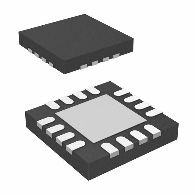


 工商网监
湘ICP备2023018690号
工商网监
湘ICP备2023018690号
