Order
Now
Product
Folder
Support &
Community
Tools &
Software
Technical
Documents
Reference
Design
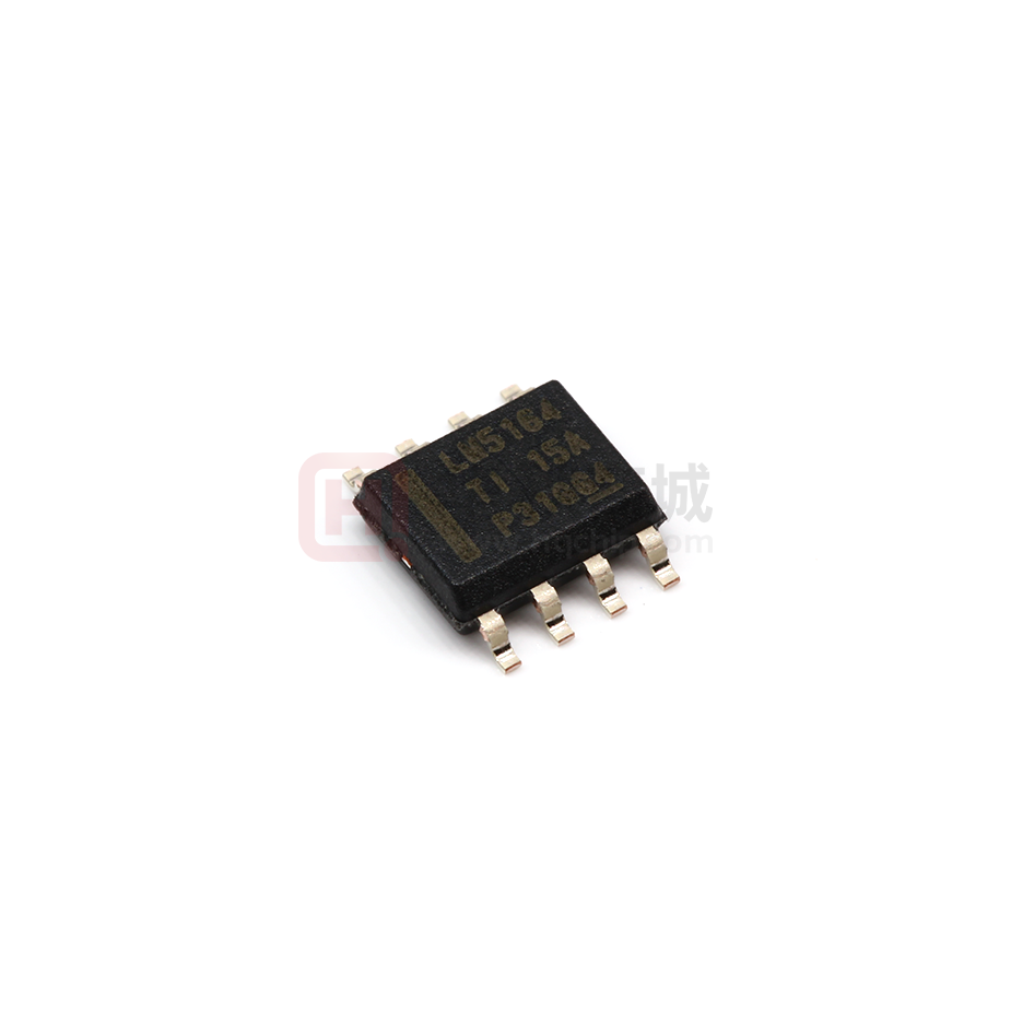
LM5164
ZHCSIT5A – SEPTEMBER 2018 – REVISED JANUARY 2019
具有超低 IQ 的 LM5164 100V 输入、1A 同步降压直流/直
直流转换器
1 特性
•
1
•
•
•
3 说明
专为可靠耐用的应用 设计
– 6V 至 100V 的宽输入电压范围
– 结温范围:–40°C 至 +150°C
– 固定 3ms 内部软启动计时器
– 峰值和谷值电流限制保护
– 输入 UVLO 和热关断保护
适用于可扩展的工业电源和电池组
– 最短导通时间和关闭时间低:50ns
– 高达 1MHz 的可调节开关频率
– 可实现高轻负载效率的二极管仿真
– 10.5µA 空载输入静态电流
– 3µA 关断静态电流
– 针对 CISPR 32 EMI 标准进行了优化
通过集成技术减小解决方案尺寸,降低成本
– COT 模式控制架构
– 集成式 0.725Ω NFET 降压开关支持宽占空比范
围
– 集成式 0.34Ω NFET 同步整流器省去了外部肖
特基二极管
– 1.2V 内部电压基准
– 无环路补偿组件
– 内部 VCC 偏置稳压器和自举二极管
– 漏极开路电源正常指示器
– 带 PowerPAD™ 的 8 引脚 SOIC 封装
使用 WEBENCH® 电源设计器创建定制设计
LM5164 同步降压转换器用于在宽输入电压范围内进行
调节,从而最大限度地减少对外部浪涌抑制组件的需
求。50ns 的最短可控导通时间有助于实现较大的降压
比,支持从 48V 标称输入到低电压轨的直接降压转
换,从而降低系统的复杂性并减少解决方案成本。
LM5164 在输入电压突降至 6V 时能够根据需要以接近
100% 的占空比继续工作,使其成为宽输入电源范围工
业和高电池节数电池组 应用。
LM5164 具有集成式高侧和低侧功率 MOSFET,可提
供高达 1A 的输出电流。恒定导通时间 (COT) 控制架
构可提供几乎恒定的开关频率,具有出色的负载和线路
瞬态响应。其他 特性 LM5164的其他特性包括超低 IQ
和二极管仿真模式运行(可实现高轻负载效率)、创新
的峰值和谷值过流保护、集成式 VCC 偏置电源和自举
二极管、精密使能和输入 UVLO 以及具有自动恢复功
能的热关断保护。开漏 PGOOD 指示器可提供进行定
序、故障报告和输出电压监视功能。
LM5164 采用热增强型 8 引脚 SO PowerPAD™ 封
装。其 1.27mm 引脚间距可以为高电压 应用提供足够
的间距。
器件信息(1)
器件型号
LM5164
封装
封装尺寸(标称值)
SO PowerPAD (8)
4.89mm × 3.90mm
(1) 如需了解所有可用封装,请参阅产品说明书末尾的可订购产品
附录。
2 应用
•
•
•
电器、电动和园艺工具
高电池节数电池组(电动自行车、电动踏板车)
电机驱动器、无人机、电信
典型应用
LO
68 µH
U1
VIN = 6 V...100 V
VIN
VOUT = 12 V
IOUT = 1 A
90
SW
EN/UVLO
RON
BST
PGOOD
80
COUT
47 µF
FB
RRON
100 k:
GND
CBST
2.2 nF RFB1
448 k:
RFB2
49.9 k:
Efficiency (%)
LM5164
CIN
2.2 µF
典型应用效率,VOUT = 12V
100
70
60
50
VIN = 14V
VIN = 24V
VIN = 48V
VIN = 72V
40
*VOUT tracks VIN if VIN < 12 V
30
0.001
0.01
0.1
1
Load (A)
1
本文档旨在为方便起见,提供有关 TI 产品中文版本的信息,以确认产品的概要。 有关适用的官方英文版本的最新信息,请访问 www.ti.com,其内容始终优先。 TI 不保证翻译的准确
性和有效性。 在实际设计之前,请务必参考最新版本的英文版本。
English Data Sheet: SNVSAU4
�LM5164
ZHCSIT5A – SEPTEMBER 2018 – REVISED JANUARY 2019
www.ti.com.cn
目录
1
2
3
4
5
6
7
特性 ..........................................................................
应用 ..........................................................................
说明 ..........................................................................
修订历史记录 ...........................................................
Pin Configuration and Functions .........................
Specifications.........................................................
1
1
1
2
3
4
6.1
6.2
6.3
6.4
6.5
6.6
4
4
4
5
5
7
Absolute Maximum Ratings ......................................
ESD Ratings..............................................................
Recommended Operating Conditions.......................
Thermal Information ..................................................
Electrical Characteristics...........................................
Typical Characteristics .............................................
Detailed Description .............................................. 9
7.1
7.2
7.3
7.4
Overview .................................................................. 9
Functional Block Diagram ....................................... 10
Feature Description................................................. 10
Device Functional Modes........................................ 15
8
Application and Implementation ........................ 16
8.1 Application Information............................................ 16
8.2 Typical Application .................................................. 16
9 Power Supply Recommendations...................... 22
10 Layout................................................................... 23
10.1 Layout Guidelines ................................................. 23
10.2 Layout Example .................................................... 25
11 器件和文档支持 ..................................................... 26
11.1
11.2
11.3
11.4
11.5
11.6
11.7
器件支持................................................................
相关文档 ...............................................................
接收文档更新通知 .................................................
社区资源................................................................
商标 .......................................................................
静电放电警告.........................................................
术语表 ...................................................................
26
26
27
27
27
27
27
12 机械、封装和可订购信息 ....................................... 27
4 修订历史记录
注:之前版本的页码可能与当前版本有所不同。
Changes from Original (September 2018) to Revision A
Page
•
首次发布生产数据数据表 ........................................................................................................................................................ 1
2
Copyright © 2018–2019, Texas Instruments Incorporated
�LM5164
www.ti.com.cn
ZHCSIT5A – SEPTEMBER 2018 – REVISED JANUARY 2019
5 Pin Configuration and Functions
DDA Package
8-Pin SO PowerPAD
Top View
GND
SW
VIN
BST
EP
EN/UVLO
PGOOD
RON
FB
Pin Functions
PIN
NO.
NAME
I/O (1)
DESCRIPTION
1
GND
G
Ground connection for internal circuits.
2
VIN
P/I
Regulator supply input pin to high-side power MOSFET and internal bias regulator. Connect
directly to the input supply of the buck converter with short, low impedance paths.
3
EN/UVLO
I
Precision enable and undervoltage lockout (UVLO) programming pin. If the EN/UVLO voltage is
below 1.1 V, the converter is in the shutdown mode with all functions disabled. If the UVLO voltage
is greater than 1.1 V and below 1.5 V, the converter is in standby mode with the internal VCC
regulator operational and no switching. If the EN/UVLO voltage is above 1.5 V, the start-up
sequence begins.
4
RON
I
On-time programming pin. A resistor between this pin and GND sets the buck switch on-time.
5
FB
I
Feedback input of voltage regulation comparator.
6
PGOOD
O
Power good indicator. This pin is an open-drain output pin. Connect to a source voltage through an
external pullup resistor between 10 kΩ to 100 kΩ
7
BST
P/I
Bootstrap gate-drive supply. Required to connect a high-quality 2.2-nF 50-V X7R ceramic capacitor
between BST and SW to bias the internal high-side gate driver.
8
SW
P
Switching node that is internally connected to the source of the high-side NMOS buck switch and
the drain of the low-side NMOS synchronous rectifier. Connect to the switching node of the power
inductor.
—
EP
—
Exposed pad of the package. No internal electrical connection. Solder the EP to the GND pin and
connect to a large copper plane to reduce thermal resistance.
(1)
G = Ground, I = Input, O = Output, P = Power
Copyright © 2018–2019, Texas Instruments Incorporated
3
�LM5164
ZHCSIT5A – SEPTEMBER 2018 – REVISED JANUARY 2019
www.ti.com.cn
6 Specifications
6.1 Absolute Maximum Ratings
Over the recommended operating junction temperature range of –40°C to +150°C (unless otherwise noted) (1)
Input voltage
Bootstrap
capacitor
MIN
MAX
VIN to GND
–0.3
100
EN to GND
–0.3
100
FB to GND
–0.3
5.5
RON to GND
–0.3
5.5
1.5
2.5
BST to GND
–0.3
105.5
BST to SW
–0.3
5.5
SW to GND
–1.5
100
External BST to SW capacitance
Output voltage
SW to GND (20-ns transient)
UNIT
V
nF
V
–3
PGOOD to GND
–0.3
14
Operating junction temperature, TJ
–40
150
°C
Storage temperature, Tstg
–65
150
°C
(1)
Stresses beyond those listed under Absolute Maximum Ratings may cause permanent damage to the device. These are stress ratings
only, which do not imply functional operation of the device at these or any other conditions beyond those indicated under Recommended
Operating Conditions. Exposure to absolute-maximum-rated conditions for extended periods may affect device reliability.
6.2 ESD Ratings
VALUE
V(ESD)
(1)
(2)
Electrostatic discharge
Human-body model (HBM), per ANSI/ESDA/JEDEC JS-001 (1)
±2000
Charged-device model (CDM), per JEDEC specification JESD22-C101 (2)
±500
UNIT
V
JEDEC document JEP155 states that 500-V HBM allows safe manufacturing with a standard ESD control process.
JEDEC document JEP157 states that 250-V CDM allows safe manufacturing with a standard ESD control process.
6.3 Recommended Operating Conditions
Over the recommended operating junction temperature range of –40°C to +150°C (unless otherwise noted)(1)
MIN
NOM
UNIT
VIN
Input voltage
100
V
VSW
Switch node voltage
100
V
VEN/UVLO
Enable voltage
100
V
ILOAD
Load current
FSW
Switching frequency
CBST
External BST to SW capacitance
tON
Programmable on-time
4
6
MAX
1
1.25
A
1000
kHz
2.2
50
nF
10000
ns
Copyright © 2018–2019, Texas Instruments Incorporated
�LM5164
www.ti.com.cn
ZHCSIT5A – SEPTEMBER 2018 – REVISED JANUARY 2019
6.4 Thermal Information
LM5164
THERMAL METRIC (1)
DDA (SOIC)
UNIT
8 PINS
RθJA
Junction-to-ambient thermal resistance
41.1
°C/W
RθJC(top)
Junction-to-case (top) thermal resistance
37.3
°C/W
RθJB
Junction-to-board thermal resistance
30.6
°C/W
ΨJT
Junction-to-top characterization parameter
6.7
°C/W
ΨJB
Junction-to-board characterization parameter
24.4
°C/W
RθJC(bot)
Junction-to-case (bottom) thermal resistance
2.4
°C/W
(1)
For more information about traditional and new thermal metrics, see the Semiconductor and IC Package Thermal Metrics application
report, SPRA953.
6.5 Electrical Characteristics
Typical values correspond to TJ = 25°C. Minimum and maximum limits apply over the full –40°C to 150°C junction
temperature range unless otherwise indicated. VIN = 24 V and VEN/UVLO = 2 V unless otherwise stated.
PARAMETER
TEST CONDITIONS
MIN
TYP
MAX
UNIT
3
15
µA
SUPPLY CURRENT
IQ-SHUTDOWN
VIN shutdown current
VEN = 0 V
IQ-SLEEP1
VIN sleep current
VEN = 2.5 V, VFB = 1.5 V
10.5
25
µA
IQ-ACTIVE
VIN active current
VEN = 2.5 V
600
880
µA
VSD-RISING
Shutdown threshold
VEN/UVLO rising
1.1
V
VSD-FALLING
Shutdown threshold
VEN/UVLO falling
0.45
VEN-RISING
Enable threshold
VEN/UVLO rising
1.45
1.5
1.55
V
VEN-FALLING
Enable threshold
VEN/UVLO falling
1.35
1.4
1.44
V
FB regulation voltage
VFB falling
1.181
1.2
1.218
V
tON1
On-time1
VVIN = 6 V, RRON = 75 kΩ
5000
ns
tON2
On-time2
VVIN = 6 V, RRON = 25 kΩ
650
ns
tON3
On-time3
VVIN = 12 V, RRON = 75 kΩ
2550
ns
tON4
On-time4
VVIN = 12 V, RRON = 25 kΩ
830
ns
VPG-UTH
FB upper threshold for PGOOD high
to low
VFB rising
1.105
1.14
1.175
V
VPG-LTH
FB lower threshold for PGOOD high to
VFB falling
low
1.055
1.08
1.1
V
VPG-HYS
PGOOD upper and lower threshold
hysteresis
VFB falling
60
mV
RPG
PGOOD pulldown resistance
VFB = 1 V
30
Ω
Gate drive UVLO
VBST rising
2.7
EN/UVLO
V
FEEDBACK
VREF
TIMING
PGOOD
BOOTSTRAP
VBST-UV
3.4
V
POWER SWITCHES
RDSON-HS
High-side MOSFET RDSON
ISW = –100 mA
0.725
Ω
RDSON-LS
Low-side MOSFET RDSON
ISW = 100 mA
0.34
Ω
Copyright © 2018–2019, Texas Instruments Incorporated
5
�LM5164
ZHCSIT5A – SEPTEMBER 2018 – REVISED JANUARY 2019
www.ti.com.cn
Electrical Characteristics (continued)
Typical values correspond to TJ = 25°C. Minimum and maximum limits apply over the full –40°C to 150°C junction
temperature range unless otherwise indicated. VIN = 24 V and VEN/UVLO = 2 V unless otherwise stated.
PARAMETER
TEST CONDITIONS
MIN
TYP
MAX
UNIT
1.75
3
4.75
ms
1.5
1.75
A
1.75
SOFT START
tSS
Internal soft-start time
CURRENT LIMIT
IPEAK1
Peak current limit threshold (HS)
1.25
IPEAK2
Peak current limit threshold (LS)
1.25
1.5
IDELTA-ILIM
Min of (IPEAK1 or IPEAK2) minus IVALLEY
200
300
IVALLEY
Valley current limit threshold
0.95
1.2
A
mA
1.4
A
THERMAL SHUTDOWN
TSD
Thermal shutdown threshold
TSD-HYS
Thermal shutdown hysteresis
6
TJ rising
175
°C
10
°C
版权 © 2018–2019, Texas Instruments Incorporated
�LM5164
www.ti.com.cn
ZHCSIT5A – SEPTEMBER 2018 – REVISED JANUARY 2019
6.6 Typical Characteristics
At TA = 25°C, VOUT = 12 V, LO = 68 µH, RRON = 105 kΩ, unless otherwise specified. .
100
100
90
90
Efficiency (%)
Efficiency (%)
80
70
60
80
50
70
VIN = 14V
VIN = 24V
VIN = 48V
VIN = 72V
40
30
0.001
VIN = 14V
VIN = 24V
VIN = 48V
VIN = 72V
60
0.01
0.1
1
0
0.2
0.4
Load (A)
图 1. Conversion Efficiency (Log Scale)
1
20
Sleep
Shutdown
Sleep
Shutdown
18
16
Quiescent Current (uA)
16
14
Current (PA)
0.8
图 2. Conversion Efficiency (Linear Scale)
20
18
0.6
Load (A)
12
10
8
6
4
14
12
10
8
6
4
2
2
0
-50
0
-25
0
25
50
75
100
Junction Temperature (qC)
125
150
0
10
20
30
D005
图 3. VIN Shutdown and Sleep Supply Current vs
Temperature
40
50
60
Input Voltage (V)
70
80
90
100
D006
图 4. VIN Shutdown and Sleep Supply Current vs Input
Voltage
600
725
590
700
Active Current (PA)
Active Current (PA)
580
675
650
625
600
570
560
550
540
530
520
575
550
-50
510
500
-25
0
25
50
75
100
Junction Temperature (qC)
125
图 5. VIN Active Current vs Temperature
版权 © 2018–2019, Texas Instruments Incorporated
150
D007
0
10
20
30
40
50
60
Input Voltage (V)
70
80
90
100
D008
图 6. VIN Active Current vs Input Voltage
7
�LM5164
ZHCSIT5A – SEPTEMBER 2018 – REVISED JANUARY 2019
www.ti.com.cn
Typical Characteristics (接
接下页)
At TA = 25°C, VOUT = 12 V, LO = 68 µH, RRON = 105 kΩ, unless otherwise specified. .
1.21
1.4
1
RDSON (:)
FB Regulation Threshold (V)
1.2
1.205
1.2
0.8
0.6
0.4
1.195
0.2
1.19
-50
-25
0
25
50
75
100
Junction Temperature (qC)
125
0
-50
150
0
25
50
75
100
Junction Temperature (qC)
125
150
D010
图 8. MOSFETs On-State Resistance vs Temperature
1.6
7
1.5
6
RRT = 105 k:
RRT = 43.2 k:
5
1.4
ON-Time (Ps)
Current Limit (A)
-25
D009
图 7. Feedback Comparator Threshold vs Temperature
1.3
1.2
4
3
2
1.1
1
Peak Current
Valley Current
1
-50
0
-25
0
25
50
75
100
Junction Temperature (qC)
125
150
D011
图 9. Peak and Valley Current Limit vs Temperature
8
High-Side FET
Low-Side FET
0
10
20
30
40
50
60
Input Voltage (V)
70
80
90
100
D012
图 10. COT On-Time vs VIN
版权 © 2018–2019, Texas Instruments Incorporated
�LM5164
www.ti.com.cn
ZHCSIT5A – SEPTEMBER 2018 – REVISED JANUARY 2019
7 Detailed Description
7.1 Overview
The LM5164 is an easy-to-use, ultra-low IQ constant on-time (COT) synchronous step-down buck regulator. With
integrated high-side and low-side power MOSFETs, the LM5164 is a low-cost, highly efficient buck converter that
operates from a wide input voltage of 6 V to 100 V, delivering up to 1 A DC load current. The LM5164 is
available in the 8-pin SO PowerPAD package. This constant on-time (COT) converter is ideal for low-noise, highcurrent, and fast load transient requirements, operating with a predictive on-time switching pulse. Over the input
voltage range, input voltage feedforward is employed to achieve a quasi-fixed switching frequency. A controllable
on-time as low as 50 ns permits high step-down ratios and a minimum forced off-time of 50 ns provides
extremely high duty-cycles allowing VIN to drop close to VOUT before frequency foldback occurs. At light loads the
device transitions into an ultra-low IQ mode to maintain high efficiency and prevent draining battery cells
connected to the input when the system is in standby. The LM5164 implements a smart peak and valley current
limit detection circuit to ensure robust protection during output short circuit conditions. Control loop compensation
is not required for this regulator, reducing design time and external component count.
The LM5164 incorporates additional features for comprehensive system requirements, including an open-drain
Power Good circuit for power-rail sequencing and fault reporting, internally-fixed soft start, monotonic start-up
into prebiased loads, precision enable for programmable line undervoltage lockout (UVLO), smart cycle-by-cycle
current limit for optimal inductor sizing, and thermal shutdown with automatic recovery. These features enable a
flexible and easy-to-use platform for a wide range of applications. The LM5164 supports a wide range of end
equipment systems requiring a regulated output from a high input supply where the transient voltage deviates
from its DC level. Examples of such end equipment systems are 48 V automotive systems, high cell count
battery pack systems, 24 V industrial systems, and 48 V telecom and PoE voltage ranges. The pin arrangement
is designed for a simple layout requiring only a few external components.
版权 © 2018–2019, Texas Instruments Incorporated
9
�LM5164
ZHCSIT5A – SEPTEMBER 2018 – REVISED JANUARY 2019
www.ti.com.cn
7.2 Functional Block Diagram
VIN
VIN
VDD
BIAS
REGULATOR
CIN
VDD UVLO
RUV1
EN/UVLO
±
+
RUV2
STANDBY
THERMAL
SHUTDOWN
1.5 V
±
+
BST
SHUTDOWN
LOGIC
0.4 V
VIN
CBST
RON
ON/OFF
TIMERS
CONSTANT
ON-TIME
CONTROL
LOGIC
RFB1
FB
FEEDBACK
COMPARATOR
VREF
VOUT
VCC
SLEEP
DETECT
±
+
RFB2
LO
SW
ZX DETECT
COUT
ZC
PGOOD
±
+
VOUT
RRON
DISABLE
PEAK/VALLEY
CURRENT LIMIT
FB
GND
±
+
PGOOD
0.9*VREF COMPARATOR
7.3 Feature Description
7.3.1 Control Architecture
The LM5164 step-down switching converter employs a constant on time (COT) control scheme. The COT control
scheme sets a fixed on-time tON of the high-side FET using a timing resistor (RON). The tON is adjusted as Vin
changes and is inversely proportion to input voltage to maintain a fixed frequency when in continuous conduction
mode (CCM). After expiration of tON, the high side FET remains off until the feedback pin is equal or below the
reference voltage of 1.2 V. In order to maintain stability, the feedback comparator requires a minimal ripple
voltage that is in phase with the inductor current during the off-time. Furthermore, this change in feedback
voltage during the off-time must be large enough to dominate any noise present at the feedback node. The
minimum recommended ripple voltage is 20 mV. Refer to 表 1 for different types of ripple injection schemes that
ensure stability over the full input voltage range.
During a rapid start-up or a positive load step, the regulator operates with minimum off-times until regulation is
achieved. This feature enables extremely fast load transient response with minimum output voltage undershoot.
When regulating the output in steady-state operation, the off-time automatically adjusts itself to produce the SWpin duty cycle required for output voltage regulation to maintain a fixed switching frequency. In CCM the
operating frequency FSW is programmed by the RRON resistor and can be calculated using 公式 1.
FSW (kHz)
10
VOUT (V) ˜ 2500
RRON (k:)
(1)
版权 © 2018–2019, Texas Instruments Incorporated
�LM5164
www.ti.com.cn
ZHCSIT5A – SEPTEMBER 2018 – REVISED JANUARY 2019
Feature Description (接
接下页)
表 1. Ripple Generation Methods
TYPE 1
TYPE 2
TYPE 3
Lowest Cost
Reduced Ripple
Minimum Ripple
LO
VIN
VIN
LM5164
CIN
VOUT
LO
VIN
VIN
SW
EN/UVLO
LM5164
CBST
BST
RFB 1
CIN
RESR
VOUT
EN/UVLO
LO
VIN
SW
VIN
RA
LM5164
CBST
BST
CFF
RFB 1
CIN
RESR
VOUT
SW
EN/UVLO
BST
CA
CBST
RFB1
CB
RON
FB
GND
PGOOD
RFB2
RRON
RESR t
RESR
20mV ˜ VOUT
VFB1 ˜ 'IL(nom)
VOUT
t
2 ˜ VIN ˜ FSW ˜ COUT
COUT
(3)
FB
GND
PGOOD
RFB2
RRON
RESR t
(2)
RON
RESR t
CFF t
20mV
'IL(nom)
VOUT
2 ˜ VIN ˜ FSW ˜ COUT
2S ˜ FSW
1
˜ (RFB1 || RFB2 )
COUT
RON
FB
GND
PGOOD
RRON
CA t
COUT
RFB2
10
FSW ˜ (RFB1 || RFB2 )
(7)
(4) R C d
A A
VIN-nom
(5)
VOUT ˜ t ON
20mV
t TR-settling
(6) CB t 3 ˜ R
FB1
@VIN-nom
(8)
(9)
表 1 presents 3 different methods for generating appropriate voltage ripple at the feedback node. Type-1 ripple
generation method uses a single resistor, RESR in series with the output capacitor. The generated voltage ripple
has two components, capacitive ripple caused by the inductor ripple current charging and discharging the output
capacitor and resistive ripple caused by the inductor ripple current flowing into the output capacitor and through
series resistance RESR. The capacitive ripple component is out of phase with the inductor current and does not
decrease monotonically during the off-time. The resistive ripple component is in phase with the inductor current
and decreases monotonically during the off-time. The resistive ripple must exceed the capacitive ripple at VOUT
for stable operation. If this condition is not satisfied, unstable switching behavior is observed in COT converters,
with multiple on-time bursts in close succession followed by a long off time. 公式 2 and 公式 3 define the value of
the series resistance RESR to ensure sufficient in-phase ripple at the feedback node.
Type-2 ripple generation uses a CFF capacitor in addition to the series resistor. As the output voltage ripple is
directly AC-coupled by Cff to the feedback node, the RESR and ultimately the output voltage ripple are reduced by
a factor of VOUT / VFB1.
Type-3 ripple generation uses an RC network consisting of RA and CA, and the switch node voltage to generate a
triangular ramp that is in-phase with the inductor current. This triangular wave is the AC-coupled into the
feedback node with capacitor CB. Because this circuit does not use output voltage ripple, it is suited for
applications where low output voltage ripple is critical. Application note AN-1481 provides additional details on
this topic.
Diode emulation mode (DEM) prevents negative inductor current, and pulse skipping maintains highest efficiency
at light load currents by decreasing the effective switching frequency. DEM operation occurs when the
synchronous power MOSFET switches off as inductor valley current reaches zero. Here, the load current is less
than half of the peak-to-peak inductor current ripple in CCM. Turning off the low-side MOSFET at zero current
reduces switching loss, and preventing negative current conduction reduces conduction loss. Power conversion
efficiency is thus higher in a DEM converter than an equivalent forced-PWM CCM converter. With DEM
operation, the duration that both power MOSFETs remain off progressively increases as load current decreases.
When this idle duration exceeds 15 μs, the converter transitions into an ultra-low IQ mode, consuming only 10-μA
quiescent current from the input.
版权 © 2018–2019, Texas Instruments Incorporated
11
�LM5164
ZHCSIT5A – SEPTEMBER 2018 – REVISED JANUARY 2019
www.ti.com.cn
Feature Description (接
接下页)
7.3.2 Internal VCC Regulator and Bootstrap Capacitor
The LM5164 contains an internal linear regulator that is powered from VIN with a nominal output of 5 V,
eliminating the need for an external capacitor to stabilize the linear regulator. The internal VCC regulator supplies
current to internal circuit blocks including the synchronous FET driver and logic circuits. The input pin (VIN) can
be connected directly to line voltages up to 100 V. As the power MOSFET has a low total gate charge, use a low
bootstrap capacitor value to reduce the stress on the internal regulator. It is required to select a high-quality 2.2nF 50-V X7R ceramic bootstrap capacitor as specified in the Absolute Maximum Ratings. Selecting a higher
value capacitance stresses the internal VCC regulator and damages the device. A lower capacitance than
required may not be sufficient to drive the internal gate of the power MOSFET. An internal diode connects from
the linear regulator to the BST pin to replenish the charge in the high-side gate drive bootstrap capacitor when
the SW voltage is low.
7.3.3 Regulation Comparator
The feedback voltage at FB is compared to an internal 1.2 V reference. The LM5164 voltage regulation loop
regulates the output voltage by maintaining the FB voltage equal to the internal reference voltage, VREF. A
resistor divider programs the ratio from output voltage VOUT to FB. For a target VOUT setpoint, calculate RFB2
based on the selected RFB1 using 公式 10.
1.2 V
˜ RFB1
VOUT 1.2 V
RFB2
(10)
TI recommends selecting RFB1 in the range of 100 kΩ to 1 MΩ for most applications. A larger RFB1 consumes
less DC current, which is mandatory if light-load efficiency is critical. RFB1 larger than 1 MΩ is not recommended
as the feedback path becomes more susceptible to noise. It is important to route the feedback trace away from
the noisy area of the PCB and keep the feedback resistors close to the FB pin.
7.3.4 Internal Soft Start
The LM5164 employs an internal soft-start control ramp that allows the output voltage to gradually reach a
steady-state operating point, thereby reducing start-up stresses and current surges. The soft-start feature
produces a controlled, monotonic output voltage start-up. The soft-start time is internally set to 3 ms.
7.3.5 ON-Time Generator
The on-time of the LM5164 high-side FET is determined by the RRON resistor and is inversely proportional to the
input voltage, VIN. The inverse relationship with VIN results in a nearly constant frequency as VIN is varied.
Calculate the on-time using 公式 11.
t ON
V
RRON k:
VIN V ˜ 2.5
(11)
Determine the RRON resistor using 公式 12 to set a specific switching frequency in CCM.
RRON (k:)
VOUT (V) ˜ 2500
FSW (kHz)
(12)
Select RRON for a minimum on-time (at maximum VIN) greater than 50 ns for proper operation. In addition to this
minimum on-time, the maximum frequency for this device is limited to 1 MHz.
7.3.6 Current Limit
The LM5164 manages overcurrent conditions with cycle-by-cycle current limiting of the peak inductor current.
The current sensed in the high-side MOSFET is compared every switching cycle to the current limit threshold
(1.5 A). To protect the converter from potential current runaway conditions, the LM5164 includes a fold-back
valley current limit feature, set at 1.2 A, that is enabled if a peak current limit is detected. As shown in 图 11, if
the peak current in the high-side MOSFET exceeds 1.5 A (typical), the present cycle is immediately terminated
12
版权 © 2018–2019, Texas Instruments Incorporated
�LM5164
www.ti.com.cn
ZHCSIT5A – SEPTEMBER 2018 – REVISED JANUARY 2019
Feature Description (接
接下页)
regardless of the programmed on-time (tON), the high-side MOSFET is turned off and the fold-back valley current
limit is activated. The low-side MOSFET remains on until the inductor current drops below this fold-back valley
current limit, after which the next on-pulse is initiated. This method folds back the switching frequency to prevent
overheating and limits the average output current to less than 1.5 A to ensure proper short-circuit and heavy-load
protection of the LM5164.
vFB
VREF
iL
Peak ILIM
IAVG(ILIM)
Valley ILIM
IAVG1
t
tON
< tON
tSW
> tSW
图 11. Current Limit Timing Diagram
Current is sensed after a leading-edge blanking time following the high-side MOSFET turnon transition. The
propagation delay of the current limit comparator is 100 ns. During high step-down conditions when the on-time
is less than 100 ns, a back-up peak current limit comparator in the low-side FET also set at 1.5 A will enable the
fold-back valley current limit set at 1.2 A. This innovative current limit scheme enables ultra-low duty-cycle
operation permitting large step down voltage conversions while ensuring robust protection of the converter.
7.3.7 N-Channel Buck Switch and Driver
The LM5164 integrates an N-channel buck switch and associated floating high-side gate driver. The gate-driver
circuit works in conjunction with an external bootstrap capacitor and an internal high-voltage bootstrap diode. A
high quality 2.2-nF 50-V X7R ceramic capacitor connected between the BST and SW pins provides the voltage
to the high-side driver during the buck switch on-time. See Internal VCC Regulator and Bootstrap Capacitor for
limitations. During the off-time, the SW pin is pulled down to approximately 0 V, and the bootstrap capacitor
charges from the internal VCC through the internal bootstrap diode. The minimum off-timer, set to 50 ns (typical),
ensures a minimum time each cycle to recharge the bootstrap capacitor. When the on-time is less than 300ns,
the minimum off-timer is forced to 250 ns to ensure that the BST capacitor is charged in a single cycle. This is
vital during wake up from sleep mode when the BST capacitor is most likely discharged.
7.3.8 Synchronous Rectifier
The LM5164 provides an internal low-side synchronous rectifier N-channel MOSFET. This MOSFET provides a
low-resistance path for the inductor current to flow when the high-side MOSFET is turned off.
The synchronous rectifier operates in a diode emulation mode. Diode emulation enables the regulator to operate
in a pulse-skipping mode during light load conditions. This mode leads to a reduction in the average switching
frequency at light loads. Switching losses and FET gate driver losses, both of which are proportional to switching
frequency, are significantly reduced at very light loads and efficiency is improved. This pulse-skipping mode also
reduces the circulating inductor current and losses associated with conventional CCM at light loads.
版权 © 2018–2019, Texas Instruments Incorporated
13
�LM5164
ZHCSIT5A – SEPTEMBER 2018 – REVISED JANUARY 2019
www.ti.com.cn
Feature Description (接
接下页)
7.3.9 Enable/Undervoltage Lockout (EN/UVLO)
The LM5164 contains a dual-level EN/UVLO circuit. When the EN/UVLO voltage is below 1.1 V (typical), the
converter is in a low-current shutdown mode and the input quiescent current (IQ) is dropped down to 3 µA. When
the voltage is greater than 1.1 V but less than 1.5 V (typical), the converter is in standby mode. In standby mode
the internal bias regulator is active while the control circuit is disabled. When the voltage exceeds the rising
threshold of 1.5 V (typical), normal operation begins. Install a resistor divider from VIN to GND to set the
minimum operating voltage of the regulator. Use 公式 13 and 公式 14 to calculate the input UVLO turn-on and
turn-off voltages, respectively.
VIN(on)
VIN(off)
§
RUV1 ·
1.5 V ˜ ¨ 1
¸
© RUV2 ¹
§
RUV1 ·
1.4 V ˜ ¨ 1
¸
© RUV2 ¹
(13)
(14)
TI recommends selecting RUV1 in the range of 1 MΩ for most applications. A larger RUV1 consumes less DC
current, which is mandatory if light-load efficiency is critical. If input UVLO is not required, the power-supply
designer can either drive EN/UVLO as an enable input driven by a logic signal or connect it directly to VIN. If
EN/UVLO is directly connected to VIN, the regulator begins switching as soon as the internal bias rails are
active.
7.3.10 Power Good (PGOOD)
The LM5164 provides a PGOOD flag pin to indicate when the output voltage is within the regulation level. Use
the PGOOD signal for start-up sequencing of downstream converters or for fault protection and output
monitoring. PGOOD is an open-drain output that requires a pullup resistor to a DC supply not greater than 14 V.
The typical range of pullup resistance is 10 kΩ to 100 kΩ. If necessary, use a resistor divider to decrease the
voltage from a higher voltage pullup rail. When the FB voltage exceeds 95% of the internal reference VREF, the
internal PGOOD switch turns off and PGOOD can be pulled high by the external pullup. If the FB voltage falls
below 90% of VREF, an internal 25-Ω PGOOD switch turns on and PGOOD is pulled low to indicate that the
output voltage is out of regulation. The rising edge of PGOOD has a built-in deglitch delay of 5 µs.
7.3.11 Thermal Protection
The LM5164 includes an internal junction temperature monitor to protect the device in the event of a higher than
normal junction temperature. If the junction temperature exceeds 175°C (typical), thermal shutdown occurs to
prevent further power dissipation and temperature rise. The LM5164 initiates a restart sequence when the
junction temperature falls to 165°C, based on a typical thermal shutdown hysteresis of 10°C. This is a nonlatching protection, and, as such, the device will cycle into and out of thermal shutdown if the fault persists.
14
版权 © 2018–2019, Texas Instruments Incorporated
�LM5164
www.ti.com.cn
ZHCSIT5A – SEPTEMBER 2018 – REVISED JANUARY 2019
7.4 Device Functional Modes
7.4.1 Shutdown Mode
EN/UVLO provides ON and OFF control for the LM5164. When VEN/UVLO is below approximately 1.1 V, the
device is in shutdown mode. Both the internal linear regulator and the switching regulator are off. The quiescent
current in shutdown mode drops to 3 µA at VIN = 24 V. The LM5164 also employs internal bias rail undervoltage
protection. If the internal bias supply voltage is below its UV threshold, the regulator remains off.
7.4.2 Active Mode
The LM5164 is in active mode when VEN/UVLO is above the precision enable threshold and the internal bias rail is
above its UV threshold. In COT active mode, the LM5164 is in one of three modes depending on the load
current:
1. CCM with fixed switching frequency when load current is above half of the peak-to-peak inductor current
ripple
2. Pulse skipping and diode emulation mode (DEM) when the load current is less than half of the peak-to-peak
inductor current ripple in CCM operation
3. Current limit CCM with peak and valley current limit protection when an overcurrent condition is applied at
the output.
7.4.3 Sleep Mode
Control Architecture gives a brief introduction to the LM5164 diode emulation (DEM) feature. The converter
enters DEM during light-load conditions when the inductor current decays to zero and the synchronous MOSFET
is turned off to prevent negative current in the system. In the DEM state, the load current is lower than half the
peak-to-peak inductor current ripple and the switching frequency decreases when the load is further decreased
as the device operates in a pulse skipping mode. A switching pulse is set when VFB drops below 1.2 V.
As the frequency of operation decreases and VFB remains above 1.2 V (VREF) with the output capacitor sourcing
the load current for greater than 15 µs, the converter enters an ultra-low IQ sleep mode to prevent draining the
input power supply. The input quiescent current (IQ) required by the LM5164 decreases to 10 µA in sleep mode,
improving the light-load efficiency of the regulator. In this mode all internal controller circuits are turned off to
ensure very low current consumption by the device. Such low IQ renders the LM5164 as the best option to
extend operating lifetime for off-battery applications. The FB comparator and internal bias rail are active to detect
when the FB voltage drops below the internal reference VREF and the converter transitions out of sleep mode into
active mode. There is a 9 µs wake-up delay from sleep to active states.
版权 © 2018–2019, Texas Instruments Incorporated
15
�LM5164
ZHCSIT5A – SEPTEMBER 2018 – REVISED JANUARY 2019
www.ti.com.cn
8 Application and Implementation
注
Information in the following applications sections is not part of the TI component
specification, and TI does not warrant its accuracy or completeness. TI’s customers are
responsible for determining suitability of components for their purposes. Customers should
validate and test their design implementation to confirm system functionality.
8.1 Application Information
The LM5164 requires only a few external components to step down from a wide range of supply voltages to a
fixed output voltage. Several features are integrated to meet system design requirements, including precision
enable, input voltage UVLO, internal soft start, programmable switching frequency, and a PGOOD indicator.
To expedite and streamline the process of designing of a LM5164-based converter, a comprehensive LM5164
Quickstart calculator is available for download to assist the designer with component selection for a given
application. This tool is complemented by the availability of an evaluation module (EVM), numerous PSPICE
models, as well as TI's WEBENCH® Power Designer.
8.2 Typical Application
For step-by-step design procedure, circuit schematics, bill of materials, PCB files, simulation and test results of
an LM5164-powered implementation, see TI Designs reference design library.
The schematic of a 12-V, 1-A COT converter is shown in 图 12.
VIN
SW
LM5164
CIN
2.2 PF
VOUT = 12 V
IOUT = 1 A
LO
68 PH
U1
VIN = 15 V...100 V
EN/UVLO
CBST
2.2 nF
CA
RA
453 k: 3.3 nF
BST
RON
FB
GND
PGOOD
RRON
100 k:
CB
56 pF
RFB1
453 k:
COUT
47 PF
RFB2
49.9 k:
Copyright © 2018, Texas Instruments Incorporated
图 12. Typical Application VIN(nom) = 48 V, VOUT = 12 V, IOUT(max) = 1 A, FSW(nom) = 300 kHz
注
This and subsequent design examples are provided herein to showcase the LM5164
converter in several different applications. Depending on the source impedance of the
input supply bus, an electrolytic capacitor may be required at the input to ensure stability,
particularly at low input voltage and high output current operating conditions. See Power
Supply Recommendations for more detail.
16
版权 © 2018–2019, Texas Instruments Incorporated
�LM5164
www.ti.com.cn
ZHCSIT5A – SEPTEMBER 2018 – REVISED JANUARY 2019
8.2.1 Design Requirements
The target full-load efficiency is 92% based on a nominal input voltage of 48 V and an output voltage of 12 V.
The required input voltage range is 15 V to 100 V. The LM5164 delivers a fixed 12 V output voltage. The
switching frequency is set by resistor RRON at 300 kHz. The output voltage soft-start time is 3 ms. The required
components are listed in 表 2. Refer to the LM5164-Q1EVM-041 EVM user's guide for more detail.
表 2. List of Components
COUNT
REF DES
VALUE
2
CIN
2.2 µF
Capacitor, Ceramic, 2.2µF, 100V, X7R, 10%
DESCRIPTION
CGA6N3X7R2A225K230AB
PART NUMBER
TDK
MANUFACTURER
1
COUT
22 µF
Capacitor, Ceramic, 22µF, 25V, X7R, 10%
TMK325B7226KMHT
Taiyo Yuden
1
CA
3300 pF
Capacitor, Ceramic, 3300pF, 16V, X7R, 10%
CGA3E2X7R2A332K080AA
TDK
1
CB
56 pF
Capacitor, Ceramic, 56pF, 50V, X7R, 10%
C0603C560J5GACTU
Kemet
1
CBST
2.2 nF
Capacitor, Ceramic, 2200pF, 50V, X7R, 10%
GCM155R71H222KA37D
MuRata
1
LF
68 µH
Inductor, 68 µH, 170 mΩ, >1.8A
MSS1246T-683MLB
Coilcraft
1
RRON
100 kΩ
Resistor, Chip, 100 k, 1%, 0.1 W, 0603
RG1608P-1053-B-T5
Susumu Co Ltd
1
RFB1
453 kΩ
Resistor, Chip, 453 k, 1%, 0.1 W, 0603
RT0603BRD07448KL
Yageo
1
RFB2
49.9 kΩ
Resistor, Chip, 49.9 k, 1%, 0.1 W, 0603
RG1608P-4992-B-T5
Susumu Co Ltd
1
RA
453 kΩ
Resistor, Chip, 453 k, 1%, 0.1W, 0603
RT0603BRD07453KL
Yageo
1
U1
Wide VIN synchronous buck converter
LM5164DDAR
TI
8.2.2 Detailed Design Procedure
8.2.2.1 Custom Design With WEBENCH® Tools
Click here to create a custom design using the LM5164 device with the WEBENCH® Power Designer.
1. Start by entering the input voltage (VIN), output voltage (VOUT), and output current (IOUT) requirements.
2. Optimize the design for key parameters such as efficiency, footprint, and cost using the optimizer dial.
3. Compare the generated design with other possible solutions from Texas Instruments.
The WEBENCH Power Designer provides a customized schematic along with a list of materials with real-time
pricing and component availability.
In most cases, these actions are available:
• Run electrical simulations to see important waveforms and circuit performance
• Run thermal simulations to understand board thermal performance
• Export customized schematic and layout into popular CAD formats
• Print PDF reports for the design, and share the design with colleagues
Get more information about WEBENCH tools at www.ti.com/WEBENCH.
8.2.2.2 Switching Frequency (RRON)
The switching frequency of LM5164 is set by the on-time programming resistor placed at RON. As shown by 公
式 15, a standard 100 kΩ, 1% resistor sets the switching frequency at 300 kHz.
RRON (k:)
VOUT (V) ˜ 2500
FSW (kHz)
(15)
Note that at very low duty cycles, the 50 ns minimum controllable on-time of the high-side MOSFET, tON(min),
limits the maximum switching frequency. In CCM, tON(min) limits the voltage conversion step-down ratio for a given
switching frequency. Calculate the minimum controllable duty cycle using 公式 16.
DMIN
t ON(min) ˜ FSW
(16)
Ultimately, the choice of switching frequency for a given output voltage affects the available input voltage range,
solution size and efficiency. The maximum supply voltage for a given tON(min) before switching frequency
reduction occurs is given by 公式 17.
版权 © 2018–2019, Texas Instruments Incorporated
17
�LM5164
ZHCSIT5A – SEPTEMBER 2018 – REVISED JANUARY 2019
VIN(max)
VOUT
t ON(min) ˜ FSW
www.ti.com.cn
(17)
8.2.2.3 Buck Inductor (LO)
The inductor ripple current (assuming CCM operation) and peak inductor current are given respectively by 公式
18 and 公式 19.
'IL
VOUT §
VOUT ·
˜ ¨1
¸
FSW ˜ LO ©
VIN ¹
IL(peak)
IOUT(max)
(18)
'IL
2
(19)
For most applications, choose an inductance such that the inductor ripple current, ΔIL, is between 30% and 50%
of the rated load current at nominal input voltage. Calculate the inductance using 公式 20.
LO
§
VOUT
˜ ¨1
¨
V
IN(nom)
©
VOUT
FSW ˜ 'IL
·
¸
¸
¹
(20)
Choosing a 68 μH inductor in this design results in 447 mA peak-to-peak ripple current at a nominal input voltage
of 48 V, equivalent to 45% of the 1 A rated load current.
Check the inductor data sheet to make sure the saturation current of the inductor is well above the current limit
setting of the LM5164. Ferrite-core inductors have relatively lower core losses and are preferred at high switching
frequencies, but exhibit a hard saturation characteristic – the inductance collapses abruptly when the saturation
current is exceeded. This results in an abrupt increase in inductor ripple current, higher output voltage ripple, and
reduced efficiency in turn compromising reliability. Note that inductor saturation current levels generally decrease
as the core temperature increases.
8.2.2.4 Output Capacitor (COUT)
Select a ceramic output capacitor to limit the capacitive voltage ripple at the converter output. This is the
sinusoidal ripple voltage that is generated from the triangular inductor current ripple flowing into and out of the
capacitor. Select an output capacitance using 公式 21 to limit the voltage ripple component to 0.5% of the output
voltage.
COUT t
8 ˜ FSW
'IL
˜ VOUT(ripple)
(21)
Substituting ΔIL(nom) of 447 mA gives COUT greater than 3.1 μF. With voltage coefficients of ceramic capacitors
taken in consideration, a 22-µF, 25-V rated capacitor with X7R dielectric is selected.
8.2.2.5 Input Capacitor (CIN)
An input capacitor is necessary to limit the input ripple voltage while providing AC current to the buck power
stage at every switching cycle. To minimize the parasitic inductance in the switching loop, position the input
capacitors as close as possible to the VIN and GND pins of the LM5164. The input capacitors conduct a squarewave current of peak-to-peak amplitude equal to the output current. It follows that the resultant capacitive
component of AC ripple voltage is a triangular waveform. Together with the ESR-related ripple component, the
peak-to-peak ripple voltage amplitude is given by 公式 22.
VIN(ripple)
IOUT ˜ D ˜ 1 D
FSW ˜ CIN
IOUT ˜ RESR
(22)
The input capacitance required for a load current, based on an input voltage ripple specification (ΔVIN), is given
by 公式 23:
18
版权 © 2018–2019, Texas Instruments Incorporated
�LM5164
www.ti.com.cn
CIN t
ZHCSIT5A – SEPTEMBER 2018 – REVISED JANUARY 2019
IOUT ˜ D ˜ 1 D
FSW ˜ VIN(ripple)
IOUT ˜ RESR
(23)
The recommended high-frequency input capacitance is 2.2 µF or higher. Ensure the input capacitor is a highquality X7S or X7R ceramic capacitor with sufficient voltage rating for CIN. Based on the voltage coefficient of
ceramic capacitors, choose a voltage rating of twice the maximum input voltage. Additionally, some bulk
capacitance is required if the LM5164 is not located within approximately 5 cm from the input voltage source.
This capacitor provides parallel damping to the resonance associated with parasitic inductance of the supply
lines and high-Q ceramics. See Power Supply Recommendations for more detail.
8.2.2.6 Type 3 Ripple Network
A Type 3 ripple generation network uses an RC filter consisting of RA and CA across SW and VOUT to generate a
triangular ramp that is in phase with the inductor current. This triangular ramp is then AC-coupled into the
feedback node using capacitor CB as shown in 图 12. Type 3 ripple injection is suited for applications where low
output voltage ripple is crucial.
Calculate RA and CA using 公式 24 and 公式 25 to provide the required ripple amplitude at the FB pin.
CA t
10
FSW ˜ RFB1 RFB2
(24)
For the feedback resistor values given in 图 12, 公式 24 dictates a minimum CA of 742 pF. In this design, a 3300
pF capacitance is chosen. This is done to keep RA within practical limits between 100 kΩ and 1 MΩ when using
公式 25.
R A CA t
VIN(nom)
VOUT ˜ t ON(nom)
20mV
(25)
Based on CA set at 3.3 nF, RA is calculated to be 453 kΩ to provide a 20-mV ripple voltage at FB. The general
recommendation for a Type 3 network is to calculate RA and CA to get 20 mV of ripple at typical operating
conditions, while ensuring a 12-mV minimum ripple voltage on FB at minimum VIN.
While the amplitude of the generated ripple does not affect the output voltage ripple, it impacts the output
regulation as it reflects as a DC error of approximately half the amplitude of the generated ripple. For example, a
converter circuit with Type 3 network that generates a 40-mV ripple voltage at the feedback node has
approximately 10-mV worse load regulation scaled up through the FB divider to VOUT than the same circuit that
generates a 20-mV ripple at FB. Calculate the coupling capacitance CB using 公式 26.
t TR-settling
CB t
3 ˜ RFB1
where
•
tTR-settling is desired load transient response settling time
(26)
CB calculates to 56 pF based on a 75-µs settling time. This value avoids excessive coupling capacitor discharge
by the feedback resistors during sleep intervals when operating at light loads. To avoid capacitance fall-off with
DC bias, use a C0G or NP0 dielectric capacitor for CB.
版权 © 2018–2019, Texas Instruments Incorporated
19
�LM5164
ZHCSIT5A – SEPTEMBER 2018 – REVISED JANUARY 2019
www.ti.com.cn
8.2.3 Application Curves
100
100
90
90
Efficiency (%)
Efficiency (%)
80
70
60
50
70
VIN = 14V
VIN = 24V
VIN = 48V
VIN = 72V
40
30
0.001
80
VIN = 14V
VIN = 24V
VIN = 48V
VIN = 72V
60
0.01
0.1
1
0
Load (A)
0.2
0.4
0.6
0.8
1
Load (A)
图 13. Conversion Efficiency (Log Scale)
图 14. Conversion Efficiency (Linear Scale)
12.4
12.3
Output Voltage (V)
12.2
12.1
12
11.9
VIN = 15V
VIN = 24V
VIN = 36V
VIN = 48V
VIN = 60V
11.8
11.7
11.6
0
0.2
0.4
0.6
Output Current (A)
0.8
1
VIN = 24 V
图 15. Load and Line Regulation Performance
VIN = 24 V
IOUT = 0 A
图 17. No-Load Start-up with VIN
20
IOUT = 0.25 A to 1 A at 0.1 A/μs
图 16. Load Step Response
VIN = 24 V
IOUT = 1 A (Resistive)
图 18. Full-Load Start-up with VIN
版权 © 2018–2019, Texas Instruments Incorporated
�LM5164
www.ti.com.cn
ZHCSIT5A – SEPTEMBER 2018 – REVISED JANUARY 2019
VIN = 24 V
IOUT = 0 A
图 19. No-Load Start-up and Shutdown with EN/UVLO
VIN = 24 V
IOUT = 0 A
VIN = 24 V
图 20. Full-Load Start-up and Shutdown with EN/UVLO
VIN = 24 V
图 21. Pre-bias Start-up with EN/UVLO
VIN = 24 V
Load = Short to 0 A
图 23. Short Circuit Recovery
版权 © 2018–2019, Texas Instruments Incorporated
IOUT = 1 A (Resistive)
Load = 0 A to Short
图 22. Short Circuit Applied
VIN = 24 V
Load = 0 A to Short to 0 A
图 24. No Load to Short Circuit/Short Circuit Recovery
21
�LM5164
ZHCSIT5A – SEPTEMBER 2018 – REVISED JANUARY 2019
VIN = 24 V
www.ti.com.cn
IOUT = 0 A
图 25. No-Load Switching
VIN = 24 V
IOUT = 1 A
图 26. Full-Load Switching
9 Power Supply Recommendations
The LM5164 buck converter is designed to operate from a wide input voltage range between 6 V and 100 V. The
characteristics of the input supply must be compatible with the Absolute Maximum Ratings and Recommended
Operating Conditions tables. In addition, the input supply must be capable of delivering the required input current
to the fully-loaded regulator. Estimate the average input current with 公式 27.
VOUT ˜ IOUT
VIN ˜ K
IIN
where
•
η is the efficiency
(27)
If the converter is connected to an input supply through long wires or PCB traces with a large impedance, take
special care to achieve stable performance. The parasitic inductance and resistance of the input cables may
have an adverse affect on converter operation. The parasitic inductance in combination with the low-ESR
ceramic input capacitors form an underdamped resonant circuit. This circuit can cause overvoltage transients at
VIN each time the input supply is cycled ON and OFF. The parasitic resistance causes the input voltage to dip
during a load transient. If the converter is operating close to the minimum input voltage, this dip can cause false
UVLO fault triggering and a system reset. The best way to solve such issues is to reduce the distance from the
input supply to the regulator and use an aluminum electrolytic input capacitor in parallel with the ceramics. The
moderate ESR of the electrolytic capacitor helps to damp the input resonant circuit and reduce any voltage
overshoots. A 10-μF electrolytic capacitor with a typical ESR of 0.5 Ω provides enough damping for most input
circuit configurations.
An EMI input filter is often used in front of the regulator that, unless carefully designed, can lead to instability as
well as some of the effects mentioned above. The application report Simple Success with Conducted EMI for
DC-DC Converters (SNVA489) provides helpful suggestions when designing an input filter for any switching
regulator.
22
版权 © 2018–2019, Texas Instruments Incorporated
�LM5164
www.ti.com.cn
ZHCSIT5A – SEPTEMBER 2018 – REVISED JANUARY 2019
10 Layout
10.1 Layout Guidelines
PCB layout is a critical portion of good power supply design. There are several paths that conduct high slew-rate
currents or voltages that can interact with stray inductance or parasitic capacitance to generate noise and EMI or
degrade the power supply performance.
1. To help eliminate these problems, bypass the VIN pin to GND with a low-ESR ceramic bypass capacitor with
a high-quality dielectric. Place CIN as close as possible to the LM5164 VIN and GND pins. Grounding for
both the input and output capacitors should consist of localized top-side planes that connect to the GND pin
and GND PAD.
2. Minimize the loop area formed by the input capacitor connections to the VIN and GND pins.
3. Locate the inductor close to the SW pin. Minimize the area of the SW trace or plane to prevent excessive
capacitive coupling.
4. Tie the GND pin directly to the power pad under the device and to a heat-sinking PCB ground plane.
5. Use a ground plane in one of the middle layers as a noise shielding and heat dissipation path.
6. Have a single-point ground connection to the plane. Route the ground connections for the feedback, softstart, and enable components to the ground plane. This prevents any switched or load currents from flowing
in analog ground traces. If not properly handled, poor grounding results in degraded load regulation or erratic
output voltage ripple behavior.
7. Make VIN, VOUT and ground bus connections as wide as possible. This reduces any voltage drops on the
input or output paths of the converter and maximizes efficiency.
8. Minimize trace length to the FB pin. Place both feedback resistors, RFB1 and RFB2, close to the FB pin. Place
CFF (if needed) directly in parallel with RFB1. If output setpoint accuracy at the load is important, connect the
VOUT sense at the load. Route the VOUT sense path away from noisy nodes and preferably through a layer on
the other side of a grounded shielding layer.
9. The RON pin is sensitive to noise. Thus, locate the RRON resistor as close as possible to the device and
route with minimal lengths of trace. The parasitic capacitance from RON to GND must not exceed 20 pF.
10. Provide adequate heat sinking for the LM5164 to keep the junction temperature below 150°C. For operation
at full rated load, the top-side ground plane is an important heat-dissipating area. Use an array of heatsinking vias to connect the exposed pad to the PCB ground plane. If the PCB has multiple copper layers,
these thermal vias must also be connected to inner layer heat-spreading ground planes.
10.1.1 Compact PCB Layout for EMI Reduction
Radiated EMI generated by high di/dt components relates to pulsing currents in switching converters. The larger
area covered by the path of a pulsing current, the more electromagnetic emission is generated. The key to
minimizing radiated EMI is to identify the pulsing current path and minimize the area of that path.
The critical switching loop of the buck converter power stage in terms of EMI is denoted in 图 27. The topological
architecture of a buck converter means that a particularly high di/dt current path exists in the loop comprising the
input capacitor and the integrated MOSFETs of the LM5164, and it becomes mandatory to reduce the parasitic
inductance of this loop by minimizing the effective loop area.
版权 © 2018–2019, Texas Instruments Incorporated
23
�LM5164
ZHCSIT5A – SEPTEMBER 2018 – REVISED JANUARY 2019
www.ti.com.cn
Layout Guidelines (接
接下页)
VIN
VIN
2
CIN
LM5164
High
di/dt
loop
BST
High-side
NMOS
gate driver
Q1
LO
8
Low-side
NMOS
gate driver
SW
VOUT
CO
Q2
1
GND
GND
图 27. DC/DC Buck Converter With Power Stage Circuit Switching Loop
The input capacitor provides the primary path for the high di/dt components of the high-side MOSFET's current.
Placing a ceramic capacitor as close as possible to the VIN and GND pins is the key to EMI reduction. Keep the
trace connecting SW to the inductor as short as possible and just wide enough to carry the load current without
excessive heating. Use short, thick traces or copper pours (shapes) for current conduction path to minimize
parasitic resistance. Place the output capacitor close to the VOUT side of the inductor, and connect the capacitor's
return terminal to the GND pin and exposed PAD of the LM5164.
10.1.2 Feedback Resistors
Reduce noise sensitivity of the output voltage feedback path by placing the resistor divider close to the FB pin,
rather than close to the load. This reduces the trace length of FB signal and noise coupling. The FB pin is the
input to the feedback comparator, and as such is a high impedance node sensitive to noise. The output node is a
low impedance node, so the trace from VOUT to the resistor divider can be long if a short path is not available.
Route the voltage sense trace from the load to the feedback resistor divider, keeping away from the SW node,
the inductor and VIN to avoid contaminating the feedback signal with switch noise, while also minimizing the trace
length. This is most important when high feedback resistances, greater than 100 kΩ, are used to set the output
voltage. Also, route the voltage sense trace on a different layer from the inductor, SW node and VIN, such that
there is a ground plane that separates the feedback trace from the inductor and SW node copper polygon. This
provides further shielding for the voltage feedback path from switching noise sources.
24
版权 © 2018–2019, Texas Instruments Incorporated
�LM5164
www.ti.com.cn
ZHCSIT5A – SEPTEMBER 2018 – REVISED JANUARY 2019
10.2 Layout Example
图 28 shows an example layout for the PCB top layer of a 2-layer board with essential components placed on the
top side.
Type 3 ripple
injection
Connect BST cap
close to BST and SW
Place FB resistors very
close to FB & GND pins
PGOOD
connection
Thermal vias under
LM5164 PAD
Place resistor R8
close to the RON pin
VOUT
connection
Optional RC
GND
connection snubber to
reduce SW
node ringing
Connect ceramic EN/UVLO
input cap close to connection
VIN and GND
图 28. LM5164 Single-Sided PCB Layout Example
版权 © 2018–2019, Texas Instruments Incorporated
25
�LM5164
ZHCSIT5A – SEPTEMBER 2018 – REVISED JANUARY 2019
www.ti.com.cn
11 器件和文档支持
11.1 器件支持
11.1.1 第三方产品免责声明
TI 发布的与第三方产品或服务有关的信息,不能构成与此类产品或服务或保修的适用性有关的认可,不能构成此类
产品或服务单独或与任何 TI 产品或服务一起的表示或认可。
11.1.2 开发支持
• LM5164 快速入门计算器
• LM5164 仿真模型
• 如需 TI 的参考设计库,请访问 TIDesigns
• 如需 TI WEBENCH 设计环境,请访问 WEBENCH® 设计中心
11.1.2.1 使用 WEBENCH® 工具创建定制设计
请单击此处,使用 LM5164 器件并借助 WEBENCH® 电源设计器创建定制设计。
1. 首先输入输入电压 (VIN)、输出电压 (VOUT) 和输出电流 (IOUT) 要求。
2. 使用优化器拨盘优化该设计的关键参数,如效率、尺寸和成本。
3. 将生成的设计与德州仪器 (TI) 的其他可行的解决方案进行比较。
WEBENCH 电源设计器可提供定制原理图以及罗列实时价格和组件供货情况的物料清单。
在多数情况下,可执行以下操作:
• 运行电气仿真,观察重要波形以及电路性能
• 运行热性能仿真,了解电路板热性能
• 将定制原理图和布局方案以常用 CAD 格式导出
• 打印设计方案的 PDF 报告并与同事共享
有关 WEBENCH 工具的详细信息,请访问 www.ti.com.cn/WEBENCH。
11.2 相关文档
请参阅如下相关文档:
• 《LM5164-Q1EVM-041 EVM 用户指南》(SNVU620)
• 《为您的 COT 降压转换器选择理想的纹波生成网络》(SNVA776)
• 白皮书:
– 《评估适用于具有成本效益的严苛应用的宽 VIN、低 EMI 同步降压 应用
– 《电源的传导 EMI 规格概述》
– 《电源的辐射 EMI 规格概述》
• TI Designs:
– TIDA-01395 具有宽输入电压转换器和电池量表且适用于智能恒温器的 24V 交流电源级 (TIDUCW0)
• Power House 博客:
– 使用低静态电流开关进行高电压转换
• Industrial Strength 博客:
– 为工业应用中的智能传感器发送器 供电
– Industrial Strength 设计 – 第 1 部分
– 楼宇自动化趋势:预测性维护
– 楼宇自动化趋势:用于改善用户舒适度的互联传感器
• 《AN-2162:轻松解决直流/直流转换器的传导 EMI 问题》(SNVA489)
• 《汽车启动仿真器用户指南》(SLVU984)
• 《使用新的热指标》(SBVA025)
• 《半导体和 IC 封装热指标》(SPRA953)
26
版权 © 2018–2019, Texas Instruments Incorporated
�LM5164
www.ti.com.cn
ZHCSIT5A – SEPTEMBER 2018 – REVISED JANUARY 2019
11.3 接收文档更新通知
要接收文档更新通知,请导航至 TI.com.cn 上的器件产品文件夹。单击右上角的通知我进行注册,即可每周接收产
品信息更改摘要。有关更改的详细信息,请查看任何已修订文档中包含的修订历史记录。
11.4 社区资源
下列链接提供到 TI 社区资源的连接。链接的内容由各个分销商“按照原样”提供。这些内容并不构成 TI 技术规范,
并且不一定反映 TI 的观点;请参阅 TI 的 《使用条款》。
TI E2E™ 在线社区 TI 的工程师对工程师 (E2E) 社区。此社区的创建目的在于促进工程师之间的协作。在
e2e.ti.com 中,您可以咨询问题、分享知识、拓展思路并与同行工程师一道帮助解决问题。
设计支持
TI 参考设计支持 可帮助您快速查找有帮助的 E2E 论坛、设计支持工具以及技术支持的联系信息。
11.5 商标
PowerPAD, E2E are trademarks of Texas Instruments.
WEBENCH is a registered trademark of Texas Instruments.
All other trademarks are the property of their respective owners.
11.6 静电放电警告
这些装置包含有限的内置 ESD 保护。 存储或装卸时,应将导线一起截短或将装置放置于导电泡棉中,以防止 MOS 门极遭受静电损
伤。
11.7 术语表
SLYZ022 — TI 术语表。
这份术语表列出并解释术语、缩写和定义。
12 机械、封装和可订购信息
以下页面包含机械、封装和可订购信息。这些信息是指定器件的最新可用数据。数据如有变更,恕不另行通知,且
不会对此文档进行修订。如需获取此数据表的浏览器版本,请查阅左侧的导航栏。
版权 © 2018–2019, Texas Instruments Incorporated
27
�PACKAGE OPTION ADDENDUM
www.ti.com
10-Dec-2020
PACKAGING INFORMATION
Orderable Device
Status
(1)
Package Type Package Pins Package
Drawing
Qty
Eco Plan
(2)
Lead finish/
Ball material
MSL Peak Temp
Op Temp (°C)
Device Marking
(3)
(4/5)
(6)
LM5164DDAR
ACTIVE SO PowerPAD
DDA
8
2500
RoHS & Green
NIPDAUAG
Level-2-260C-1 YEAR
-40 to 150
LM5164
LM5164DDAT
ACTIVE SO PowerPAD
DDA
8
250
RoHS & Green
NIPDAUAG
Level-2-260C-1 YEAR
-40 to 150
LM5164
(1)
The marketing status values are defined as follows:
ACTIVE: Product device recommended for new designs.
LIFEBUY: TI has announced that the device will be discontinued, and a lifetime-buy period is in effect.
NRND: Not recommended for new designs. Device is in production to support existing customers, but TI does not recommend using this part in a new design.
PREVIEW: Device has been announced but is not in production. Samples may or may not be available.
OBSOLETE: TI has discontinued the production of the device.
(2)
RoHS: TI defines "RoHS" to mean semiconductor products that are compliant with the current EU RoHS requirements for all 10 RoHS substances, including the requirement that RoHS substance
do not exceed 0.1% by weight in homogeneous materials. Where designed to be soldered at high temperatures, "RoHS" products are suitable for use in specified lead-free processes. TI may
reference these types of products as "Pb-Free".
RoHS Exempt: TI defines "RoHS Exempt" to mean products that contain lead but are compliant with EU RoHS pursuant to a specific EU RoHS exemption.
Green: TI defines "Green" to mean the content of Chlorine (Cl) and Bromine (Br) based flame retardants meet JS709B low halogen requirements of


 工商网监
湘ICP备2023018690号
工商网监
湘ICP备2023018690号
