LM53625-Q1, LM53635-Q1
SNVSAA7B – DECEMBER 2015 – REVISED JULY 2021
LM53625/35-Q1, 2.5-A or 3.5-A, 36-V Synchronous, 2.1-MHz, Step-Down DC-DC
Converter
1 Features
3 Description
•
The LM53625-Q1/LM53635-Q1 synchronous buck
regulator is optimized for automotive applications,
providing an output voltage of 5 V, 3.3 V, or
an adjustable output. Advanced high-speed circuitry
allows the LM53625-Q1/LM53635-Q1 to regulate from
an input of 18 V to an output of 3.3 V at a fixed
frequency of 2.1 MHz. Innovative architecture allows
this device to regulate a 3.3-V output from an input
voltage of only 3.55 V. All aspects of the LM53625Q1/LM53635-Q1 are optimized for automotive and
performance-driven industrial customers. An input
voltage range up to 36 V, with transient tolerance
up to 42 V, eases input surge protection design.
The automotive-qualified Hotrod QFN package with
wettable flanks reduces parasitic inductance and
resistance while increasing efficiency, minimizing
switch node ringing, and dramatically lowering
electromagnetic interference (EMI). An open-drain
reset output, with built-in filtering and delay, provides
a true indication of system status. This feature
negates the requirement for an additional supervisory
component, saving cost and board space. Seamless
transition between PWM and PFM modes and
low quiescent current (only 15 µA for the 3.3 V
option) ensure high efficiency and superior transient
responses at all loads.
•
•
•
•
•
•
•
•
•
•
•
•
AEC-Q100 automotive qualified:
– Device temperature grade 1: –40°C to +125°C
ambient operating temperature range
– Device HBM classification level 2
– Device CDM classification level C6
–40°C to +150°C junction temperature range
15-µA quiescent urrent at no load (typical) with
3.3-V output
5.0-mm × 4.0-mm VQFN package with or without
wettable flanks and 0.6-mm VIN spacing
Low EMI and switch noise
Spread spectrum option
External frequency synchronization
RESET output with internal filter and 3-ms release
timer
Pin-selectable forced PWM mode
Built-in compensation, soft start, current limit,
thermal shutdown, and UVLO
0.6-V dropout at 3.5 A at 105°C TA
±1% output voltage tolerance (–40°C to 125°C TJ)
Available with fixed 5-V, 3.3-V or adjustable output
2 Applications
•
•
•
•
Telematics
Head unit
Instrumentation cluster
Battery-powered applications
Device Information
DEVICE NAME
LM53625-Q1
LM53635-Q1
(1)
PACKAGE(1)
VQFN-HR (22)
BODY SIZE
5.00 mm × 4.00 mm
For all available packages, see the orderable addendum at
the end of the data sheet.
Typical Automotive Layout (22 mm x 12.5 mm)
Typical Application Circuit
An IMPORTANT NOTICE at the end of this data sheet addresses availability, warranty, changes, use in safety-critical applications,
intellectual property matters and other important disclaimers. PRODUCTION DATA.
�LM53625-Q1, LM53635-Q1
www.ti.com
SNVSAA7B – DECEMBER 2015 – REVISED JULY 2021
Table of Contents
1 Features............................................................................1
2 Applications..................................................................... 1
3 Description.......................................................................1
4 Revision History.............................................................. 2
5 Device Comparison......................................................... 3
6 Pin Configuration and Functions...................................4
7 Specifications.................................................................. 5
7.1 Absolute Maximum Ratings........................................ 5
7.2 ESD Ratings............................................................... 5
7.3 Recommended Operating Conditions.........................6
7.4 Thermal Information....................................................6
7.5 Electrical Characteristics.............................................7
7.6 System Characteristics............................................... 9
7.7 Timing Characteristics.................................................9
7.8 Typical Characteristics.............................................. 11
8 Detailed Description......................................................13
8.1 Overview................................................................... 13
8.2 Functional Block Diagram......................................... 14
8.3 Feature Description...................................................15
8.4 Device Functional Modes..........................................20
8.5 Spread-Spectrum Operation..................................... 23
9 Application and Implementation.................................. 24
9.1 Application Information............................................. 24
9.2 Typical Applications.................................................. 24
9.3 What to Do and What Not to Do............................... 41
10 Power Supply Recommendations..............................41
11 Layout........................................................................... 42
11.1 Layout Guidelines................................................... 42
11.2 Layout Example...................................................... 43
12 Device and Documentation Support..........................44
12.1 Device Support....................................................... 44
12.2 Documentation Support.......................................... 44
12.3 Receiving Notification of Documentation Updates..44
12.4 Support Resources................................................. 44
12.5 Trademarks............................................................. 44
12.6 Electrostatic Discharge Caution..............................44
12.7 Glossary..................................................................44
13 Mechanical, Packaging, and Orderable
Information.................................................................... 44
4 Revision History
NOTE: Page numbers for previous revisions may differ from page numbers in the current version.
Changes from Revision A (May 2016) to Revision B (July 2021)
Page
• Updated the numbering format for tables, figures, and cross-references throughout the document. ................1
• Updated applications.......................................................................................................................................... 1
• Added the non-wettable flank options.................................................................................................................3
Changes from Revision * (December 2015) to Revision A (May 2016)
Page
• Product Preview to Production Data ..................................................................................................................1
2
Submit Document Feedback
Copyright © 2021 Texas Instruments Incorporated
Product Folder Links: LM53625-Q1 LM53635-Q1
�LM53625-Q1, LM53635-Q1
www.ti.com
SNVSAA7B – DECEMBER 2015 – REVISED JULY 2021
5 Device Comparison
Table 5-1. LM53625-Q1 Devices (2.5-A Output)
PART NUMBER
OUTPUT VOLTAGE
SPREAD
SPECTRUM
PACKAGE QTY
WETTABLE
FLANKS
LM53625AQRNLRQ1
Adjustable
No
3000
Y
LM53625AQRNLTQ1
Adjustable
No
250
Y
LM536253QRNLRQ1
3.3 V
No
3000
Y
LM536253QRNLTQ1
3.3 V
No
250
Y
LM536255QRNLRQ1
5V
No
3000
Y
LM536255QRNLTQ1
5V
No
250
Y
LM53625MQRNLRQ1
Adjustable
Yes
3000
Y
LM53625MQRNLTQ1
Adjustable
Yes
250
Y
LM53625NQRNLRQ1
3.3 V
Yes
3000
Y
LM53625NQRNLTQ1
3.3 V
Yes
250
Y
LM53625LQRNLRQ1
5V
Yes
3000
Y
LM53625LQRNLTQ1
5V
Yes
250
Y
LM53625NQURNLRQ1
3.3 V
Yes
3000
N
LM53625MQURNLRQ1
Adjustable
Yes
3000
N
LM53625LQURNLRQ1
5V
Yes
3000
N
Table 5-2. LM53635-Q1 Devices (3.5-A Output)
PART NUMBER
OUTPUT VOLTAGE
SPREAD
SPECTRUM
PACKAGE QTY
Wettable Flanks
LM53635AQRNLRQ1
Adjustable
No
3000
Y
LM53635AQRNLTQ1
Adjustable
No
250
Y
LM536353QRNLRQ1
3.3 V
No
3000
Y
LM536353QRNLTQ1
3.3 V
No
250
Y
LM536355QRNLRQ1
5V
No
3000
Y
LM536355QRNLTQ1
5V
No
250
Y
LM53635MQRNLRQ1
Adjustable
Yes
3000
Y
LM53635MQRNLTQ1
Adjustable
Yes
250
Y
LM53635NQRNLRQ1
3.3 V
Yes
3000
Y
LM53635NQRNLTQ1
3.3 V
Yes
250
Y
LM53635LQRNLRQ1
5V
Yes
3000
Y
LM53635LQRNLTQ1
5V
Yes
250
Y
LM53635MQURNLRQ1
Adjustable
Yes
3000
N
LM53635NQURNLRQ1
3.3 V
Yes
3000
N
Submit Document Feedback
Copyright © 2021 Texas Instruments Incorporated
Product Folder Links: LM53625-Q1 LM53635-Q1
3
�LM53625-Q1, LM53635-Q1
www.ti.com
SNVSAA7B – DECEMBER 2015 – REVISED JULY 2021
6 Pin Configuration and Functions
PGND1
PGND2
PGND2
PGND2
PGND1
PGND1
SW
PGND1
PGND2
PVIN 2
PVIN 1
AVIN
SYNC
FPWM
CBOOT
NC
VCC
EN
RESET AGND
FB
BIAS
Figure 6-1. RNL Package 22-Pin VQFN Top View
Table 6-1. Pin Functions
PIN
NO.
NAME
DESCRIPTION
1
VCC
A
Internal 3.1-V LDO output. Used as supply to internal control circuits. Connect a high-quality
4.7-µF capacitor from this pin to AGND.
2
CBOOT
P
Bootstrap capacitor connection for gate drivers. Connect a high quality 470-nF capacitor
from this pin to the SW pin.
3
SYNC
I
Synchronization input to regulator. Used to synchronize the device switching frequency to a
system clock. Triggers on rising edge of external clock; frequency must be in the range of 1.9
MHz and 2.3 MHz.
4
PVIN1
P
Input supply to regulator. Connect input bypass capacitors directly to this pin and PGND
pins. Connect PVIN1 and PVIN2 pins directly together at PCB.
5, 6, 7, 8
PGND1
G
Power ground to internal low side MOSFET. These pins must be tied together on the PCB.
Connect PGND1 and PGND2 directly together at PCB. Connect to AGND and system
ground.
SW
P
Regulator switch node. Connect to power inductor.
10, 11, 12, 13
PGND2
G
Power ground to internal low side MOSFET. These pins must be tied together. Connect
PGND1 and PGND2 directly together at PCB. Connect to AGND and system ground.
14
PVIN2
P
Input supply to regulator. Connect input bypass capacitors directly to this pin and PGND
pins. Connect PVIN1 and PVIN2 pins directly together at PCB.
15
AVIN
A
Analog VIN, Connect to PVIN1 and PVIN2 on PCB.
16
FPWM
I
Do not float. Mode control input of regulator. High = FPWM, low = Automatic light load mode.
17
NC
—
18
EN
I
Enable input to regulator. High = on, Low = off. Can be connected to VIN. Do not float.
19
RESET
O
Open drain reset output flag. Connect to suitable voltage supply through a current limiting
resistor. High = regulator OK, Low = regulator fault. Goes low when EN = low.
20
AGND
G
Analog ground for regulator and system. All electrical parameters are measured with respect
to this pin. Connect to PGND on PCB
21
FB
A
Feedback input to regulator. Connect to output voltage node for fixed VOUT options.
Connect to feedback voltage divider for adjustable option.
22
BIAS
P
Input to auxiliary bias regulator. Connect to output voltage node.
9
(1)
4
I/O(1)
No internal connection
A = Analog, O = Output, I = Input, G = Ground, P = Power
Submit Document Feedback
Copyright © 2021 Texas Instruments Incorporated
Product Folder Links: LM53625-Q1 LM53635-Q1
�LM53625-Q1, LM53635-Q1
www.ti.com
SNVSAA7B – DECEMBER 2015 – REVISED JULY 2021
7 Specifications
7.1 Absolute Maximum Ratings
over the recommended operating junction temperature range of –40°C to +150°C (unless otherwise noted)(1)
PARAMETER
VIN (AVIN,PVIN1 and PVIN2) to AGND, PGND1 and PGND2(2)
SW to AGND,
PGND(3)
CBOOT to SW
EN to AGND,
PGND(2) (4)
MIN
MAX
UNIT
–0.3
40
V
–0.3
VIN + 0.3
V
–0.3
3.6
V
–0.3
40
V
BIAS to AGND, PGND
–0.3
16
V
FB to AGND, PGND
–0.3
16
V
RESET to AGND, PGND
–0.3
8
V
RESET sink
current(5)
10
mA
SYNC to AGND,PGND(2) (4)
–0.3
40
V
FPWM to AGND,PGND(4)
–0.3
40
V
VCC to AGND,PGND
–0.3
3.6
V
Junction temperature
–40
150
°C
Storage temperature, Tstg
–40
150
°C
(1)
(2)
(3)
(4)
(5)
Stresses beyond those listed under Section 7.1 may cause permanent damage to the device. These are stress ratings only, functional
operation of the device at these or any other conditions beyond those indicated under Section 7.3 are not implied. Exposure to
absolute-maximum-rated conditions for extended periods may affect device reliability.
A maximum of 42 V can be sustained at this pin for a duration of ≤ 500 ms at a duty cycle of ≤ 0.01%.
A voltage of 2 V below PGND and 2 V above VIN can appear on this pin for ≤ 200 ns with a duty cycle of ≤ 0.01%.
Under no conditions should the voltage on this pin be allowed to exceed the voltage on the PVIN1,PVIN2 or AVIN pins by more than
0.3 V.
Do not exceed the voltage rating on this pin.
7.2 ESD Ratings
VALUE
V(ESD)
(1)
Electrostatic discharge
Human-body model (HBM), per AEC
Q100-002(1)
Charged-device model (CDM), per AEC Q100-011
±2500
±1000
UNIT
V
AEC Q100-002 indicates that HBM stressing shall be in accordance with the ANSI/ESDA/JEDEC JS-001 specification.
Submit Document Feedback
Copyright © 2021 Texas Instruments Incorporated
Product Folder Links: LM53625-Q1 LM53635-Q1
5
�LM53625-Q1, LM53635-Q1
www.ti.com
SNVSAA7B – DECEMBER 2015 – REVISED JULY 2021
7.3 Recommended Operating Conditions
over the recommended operating junction temperature range of –40°C to +150°C (unless otherwise noted)
MIN
Input voltage after
start-up(1)
NOM
MAX
3.9
UNIT
36
V
3.4
V
5.2
V
10
V
Load current for LM53625-Q1, fixed output option and adjustable
2.5
A
Load current for LM53635-Q1, fixed output option and adjustable
3.5
A
Output voltage for 3.3-V LM53625/35-Q1(2)
Output voltage for 5-V
LM53625/35-Q1(2)
Output adjustment for adjustable version of LM53625/35-Q1(2)
3.3
Junction temperature for 1000-hour lifetime
–40
125
°C
Junction temperature for 408-hour lifetime
–40
150
°C
(1)
(2)
An extended input voltage range to 3.5 V is possible; see Section 7.6 table. See Input UVLO for start-up conditions.
The output voltage must not be allowed to fall below zero volts during normal operation.
7.4 Thermal Information
LM53625/35-Q1
THERMAL METRIC(1)
RNL (VQFN)
UNIT
22 PINS
RθJA
Junction-to-ambient thermal resistance
29.4
°C/W
RθJC
Junction-to-case (top) thermal resistance
14.2
°C/W
RθJB
Junction-to-board thermal resistance
5.4
°C/W
ψJT
Junction-to-top characterization parameter
1.2
°C/W
ψJB
Junction-to-board characterization parameter
5.4
°C/W
RθJC(bot)
Junction-to-case (bottom) thermal resistance
2.4
°C/W
(1)
6
For more information about traditional and new thermal metrics, see the Semiconductor and IC Package Thermal Metrics application
report, SPRA953.
Submit Document Feedback
Copyright © 2021 Texas Instruments Incorporated
Product Folder Links: LM53625-Q1 LM53635-Q1
�LM53625-Q1, LM53635-Q1
www.ti.com
SNVSAA7B – DECEMBER 2015 – REVISED JULY 2021
7.5 Electrical Characteristics
Limits apply over the recommended operating junction temperature range of –40°C to +150°C, unless otherwise noted.
Minimum and maximum limits are specified through test, design, or statistical correlation. Typical values represent the most
likely parametric norm at Tj = 25°C, and are provided for reference purposes only. Unless otherwise stated the following
conditions apply: VIN = 13.5 V.
PARAMETER
VFB
Initial output voltage accuracy
IQ
Operating quiescent current;
measured at VIN pin when
enabled and not switching(1)
IB
Bias current into BIAS pin,
enabled, not switching
ISD
TEST CONDITIONS
VIN = 3.8 V to 36 V, TJ = 25°C
VIN = 3.8 V to 36 V
MIN
TYP
–1%
1%
–1.5%
1.5%
VIN = 13.5 V, VBIAS = 5 V
16
VIN = 13.5 V, VBIAS = 5 V, FPWM = 0
V
35
VIN = 13.5 V, VBIAS = 3.3 V, FPWM =
0V
35
EN ≤ 0.4 V, TJ = 25°C
2
EN ≤ 0.4 V, TJ = 85°C
VRESET
Minimum input voltage to operate
3
Falling
2.95
3.25
3.55
Hysteresis
0.28
0.3
0.4
105%
107%
110%
92%
94%
96.5%
Magnitude of RESET lower
Steady-state output voltage and
threshold from steady state output RESET threshold read at the same
voltage
TJ and VIN
VRESET_VALID
Minimum input voltage for proper
RESET function
Low level RESET function output
voltage
Switching frequency
FSYNC
Sync frequency range
DSYNC
Sync input duty cycle range
VFPWM
3.95
Falling, % VOUT
RESET hysteresis as a percent of
output voltage setpoint
FSW
3.55
Rising, % of VOUT
VRESET_HYST
VOL
3.2
RESET lower threshold voltage
FPWM input threshold voltage
Frequency span of spread
spectrum operation
FPSS
Spread-spectrum pattern
frequency(2)
FSW-SS
Switching Frequency while in
spread spectrum
V
96%
±1
50-µA pullup to RESET pin, EN = 0
V, TJ= 25°C
1.5
50-µA pullup to RESET pin, VIN =1.5
V, EN = 0 V
0.4
0.5-mA pullup to RESET pin, VIN
=13.5 V, EN=0 V
0.4
1-mA pullup to RESET pin, VIN
=13.5 V, EN=3.3 V
0.4
VIN = 13.5 V, center frequency with
spread spectrum, PWM operation
1.85
2.1
2.35
VIN = 13.5 V, without spread
spectrum, PWM operation
1.85
2.1
2.35
1.9
2.1
2.3
V
V
MHz
High state input < 5.5 V and > 2.3 V
25%
FPWM input high (MODE = FPWM)
1.5
MHz
75%
FPWM input low (MODE = AUTO
with diode emulation)
FPWM input hysteresis
FSSS
µA
5
Rising
RESET upper threshold voltage
µA
µA
EN ≤ 0.4V, TJ = 150°C
VIN-OPERATE
UNIT
6
VIN = 13.5 V, VBIAS = 5 V, TJ = 85°C
Shutdown quiescent current;
measured at VIN pin
MAX
0.4
0.15
V
1
±3%
9
VIN = 13.5 V, PWM operation
1.81
Hz
MHz
Submit Document Feedback
Copyright © 2021 Texas Instruments Incorporated
Product Folder Links: LM53625-Q1 LM53635-Q1
7
�LM53625-Q1, LM53635-Q1
www.ti.com
SNVSAA7B – DECEMBER 2015 – REVISED JULY 2021
Limits apply over the recommended operating junction temperature range of –40°C to +150°C, unless otherwise noted.
Minimum and maximum limits are specified through test, design, or statistical correlation. Typical values represent the most
likely parametric norm at Tj = 25°C, and are provided for reference purposes only. Unless otherwise stated the following
conditions apply: VIN = 13.5 V.
PARAMETER
TEST CONDITIONS
IFPWM
FPWM leakage current
ISYNC
SYNC leakage current
IL-HS
High-side switch current limit
IL-LS
Low-side switch current limit
IL-ZC
Zero-cross current limit FPWM =
low
IL-NEG
Negative current limit FPWM =
high
RDSON
Power switch on-resistance
TYP
1
VIN = VFPWM = 13.5 V
5
VIN = 13.5 V, VSYNC = 3.3 V
1
VIN = VSYNC = 13.5 V
5
MAX
UNIT
µA
µA
LM53625
3.5
5
6.5
LM53635
4.5
6
7.5
LM53625
2.5
3.5
4.1
LM53635
3.5
4.5
5.1
A
A
–0.02
A
–1.5
High-side MOSFET RDSON, VIN = 13
V, IL=1A
60
130
Low-side MOSFET RDSON, VIN = 13
V, IL=1A
40
80
mΩ
VEN
Enable input threshold voltage rising
VEN_HYST
Enable threshold hysteresis
VEN_WAKE
Enable wake-up threshold
IEN
EN pin input current
VCC
Internal VCC voltage
VCC_UVLO
Internal VCC input undervoltage
lockout
VIN rising
2.7
V
Hysteresis below VCC-UVLO
185
mV
IFB
Input current from FB to AGND
Adjustable LM53625/35-Q1, FB=1 V
RRESET
Enable rising
0.45
0.55
V
5
µA
V
2
3.05
VIN = 13.5 V, VBIAS = 3.3 V
3.15
TJ = 25°C
V
20
nA
0.993
1
TJ = –40°C to 125°C
0.99
1
1.01
TJ = –40°C to 150°C
0.985
1
1.015
50
85
Ω
0.4
V
Pull FB pin low. Sink 1-mA at
RESET pin
RDSON of RESEToutput
1.007
V
1.5
VIL
TSD
Thermal shutdown thresholds(2)
DMAX
Maximum switch duty cycle
(2)
V
VIN 13.5 V, VBIAS = 0 V
VHYST
(1)
2
0.4
VIH
VSYNC
1.7
VIN = VEN = 13.5 V
Reference voltage for adjustable
option only
VREF
8
MIN
VIN = 13.5 V, VFPWM = 3.3 V
Rising
0.15
1
155
175
Hysteresis
15
Fsw = 2.1 MHz
While in
dropout(2)
°C
80%
98%
This is the current used by the device while not switching, open loop on the ATE. It does not represent the total input current from the
regulator system.
Ensured by Design, Not tested at production.
Submit Document Feedback
Copyright © 2021 Texas Instruments Incorporated
Product Folder Links: LM53625-Q1 LM53635-Q1
�LM53625-Q1, LM53635-Q1
www.ti.com
SNVSAA7B – DECEMBER 2015 – REVISED JULY 2021
7.6 System Characteristics
The following specifications are ensured by design provided that the component values in the typical application circuit
are used. These parameters are not ensured by production testing. Limits apply over the recommended operating junction
temperature range of –40°C to +150°C, unless otherwise noted. Minimum and maximum limits are specified through test,
design, or statistical correlation. Typical values represent the most likely parametric norm at TJ = 25°C, and are provided for
reference purposes only. Unless otherwise stated the following conditions apply: VIN = 13.5 V.
PARAMETER
VIN-MIN
VOUT
IQ-VIN
TEST CONDITIONS
MIN
TYP
MAX
Minimum input voltage for full
functionality at 1.5 A load, after startup.
VOUT = 3.3 V +2/–3% regulation
Minimum input voltage for full
functionality at maximum rated load
3.5 A after start-up.
VOUT = 3.3 V +2/–3% regulation
Output voltage for 5-V option
VIN = 5.6 V to 36 V, IOUT = 3.5 A
4.925
5
5.08
Output voltage for 3.3-V option
VIN 3.9 V to 36 V, IOUT = 3.5 A
3.24
3.3
3.35
Output voltage for 5-V option
VIN = 5.5 V to 36 V, IOUT = 100 µA to 100
mA
4.92
5.05
5.125
Output voltage for 3.3-V option
VIN = 3.8 V to 36 V, IOUT = 100 µA to 100
mA
3.24
3.33
3.38
Output voltage for adjustable option
VIN = VOUT + 1 V to 36 V, IOUT = 3.5 A
Input current to VIN pin
UNIT
3.5
V
3.9
–2.25%
2.25%
VIN= 13.5 V, VOUT = 3.3 V, IOUT = 0 A
FPWM = 0
15
VIN = 13.5 V, VOUT = 5.0 V and IOUT = 0 A
FPWM = 0
20
VDROP1
Minimum input to output voltage
differential to maintain regulation
accuracy without inductor DCR drop
VOUT = 3.3 V/5 V, IOUT= 3.5 A, +2/–3%
output accuracy
VDROP2
Minimum input to output voltage
differential to maintain FSW ≥ 1.85
MHz without inductor DCR drop
VOUT = 3.3 V/5 V, IOUT=3.5 A, FSW = 1.85
MHz, 2% regulation accuracy
Efficiency
Typical Efficiency without inductor
loss
V
40
µA
0.35
0.6
V
1.1
1.4
V
VIN = 13.5 V, VOUT= 5.0 V, IOUT = 3.5 A
90%
VIN = 13.5 V, VOUT = 3.3 V, IOUT = 3.5 A
84%
VIN = 13.5 V, VOUT = 5 V, IOUT = 100 mA
88%
7.7 Timing Characteristics
Limits apply over the recommended operating junction temperature range of –40°C to +150°C, unless otherwise noted.
Minimum and maximum limits are ensured through test, design or statistical correlation. Typical values represent the most
likely parametric norm at TJ = 25°C, and are provided for reference purposes only. Unless otherwise stated the following
conditions apply: VIN = 13.5 V.
MIN
NOM
MAX
65
84
UNIT
60
80
ns
3
4
ms
12
25
45
µs
2
3.2
5
ms
tON
Minimum switch on time, VIN = 18 V, IL=1 A
tOFF
Minimum switch off time, VIN = 3.8 V, IL=1 A
tRESET-act
Delay time to RESET high signal
tRESET-filter
Glitch filter time for RESET function(1)
tSS
Soft-Start Time from first switching pulse to VREF at 90%
tEN
Turn-on delay, CVCC = 2.2 µF(2)
1
ms
tW
Short circuit wait time (hiccup time)(3)
6
ms
Change transition time from AUTO to FPWM MODE, 20-mA load,
VIN = 13.5 V
100
µs
Change transition time from FPWM to AUTO MODE, 20-mA load,
VIN = 13.5 V
80
µs
tFPWM
(1)
(2)
2
ns
See Section 8.
This is the time from the rising edge of EN to the time that the soft-start ramp begins.
Submit Document Feedback
Copyright © 2021 Texas Instruments Incorporated
Product Folder Links: LM53625-Q1 LM53635-Q1
9
�LM53625-Q1, LM53635-Q1
SNVSAA7B – DECEMBER 2015 – REVISED JULY 2021
(3)
10
www.ti.com
Tw is the wait time between current limit trip and re-start. Tw is nominally 4× the soft-start time. However, provision must be made to
make Tw longer to ensure survivability during an output short circuit.
Submit Document Feedback
Copyright © 2021 Texas Instruments Incorporated
Product Folder Links: LM53625-Q1 LM53635-Q1
�LM53625-Q1, LM53635-Q1
www.ti.com
SNVSAA7B – DECEMBER 2015 – REVISED JULY 2021
7.8 Typical Characteristics
Unless otherwise specified the following conditions apply: VIN = 12 V, TA = 25°C. Specified temperatures are
ambient.
2.2
100.2%
100.1%
2.175
Switching Frequency (MHz)
Reference Voltage Drift
100%
99.9%
99.8%
99.7%
99.6%
99.5%
99.4%
2.15
2.125
2.1
2.075
2.05
2.025
99.3%
99.2%
-40
-20
0
20
40
60
80 100
Temperature (qC)
120
140
2
-50
160
VIN = 12 V
25
50
75
Temperature (qC)
100
125
150
D023
Figure 7-2. Switching Frequency vs Temperature
4.8
6.4
6.2
LM53635
LM53625
4.6
6
5.8
4.4
5.6
4.2
Current (A)
Current (A)
0
VIN = 12 V
Figure 7-1. Reference Voltage Drift
5.4
5.2
5
4
3.8
4.8
4.6
3.6
4.4
LM53635
LM53625
4.2
4
-40
-20
0
20
40
60
80 100
Temperature (qC)
120
140
3.4
3.2
-40
160
-20
0
20
D034
VIN = 12 V
40
60
80 100
Temperature (qC)
120
140
160
D035
VIN = 12V
Figure 7-3. High Side/Peak Current Limit for
LM53625/35-Q1
Figure 7-4. Low Side/Valley Current Limit for
LM53625/35-Q1
14
0.065
0.06
0.055
0.05
0.045
0.04
0.035
0.03
0.025
0.02
0.015
0.01
0.005
0
5 Vin
8 Vin
12 Vin
13.5 Vin
18 Vin
36 Vin
12
10
Current (PA)
Input Current (A)
-25
D024
8
6
4
2
0
5
10
15
20
25
Input Voltage (V)
30
35
40
0
-40
-20
0
D004
VIN = 12 V
Figure 7-5. Short Circuit Average Input Current for
LM53635-Q1
20
40
60
80 100
Temperature (qC)
120
140
160
D028
VIN = 12 V
Figure 7-6. Shutdown Current
Submit Document Feedback
Copyright © 2021 Texas Instruments Incorporated
Product Folder Links: LM53625-Q1 LM53635-Q1
11
�LM53625-Q1, LM53635-Q1
www.ti.com
SNVSAA7B – DECEMBER 2015 – REVISED JULY 2021
5.4
108%
VRESET_UPPER
VRESET_UPPER
5.3
VRESET_UPPER_FALLING
% of Vout at no load
5.2
106%
Voltage (V)
5.1
VOUT
5
4.9
4.8
4.7
VRESET_LOWER_RISING
VRESET_LOWER
104%
102%
100%
98%
96%
4.6
4.5
-40
-20
0
20
40
60
80 100
Termperature (qC)
120
140
160
D026
Figure 7-7. RESET Threshold Fixed 5-V output
12
94%
-40
VRESET_LOWER
-20
0
20
40
60
80 100
Temperature (qC)
120
140
160
D027
Figure 7-8. RESET Threshold as Percentage of
Output Voltage
Submit Document Feedback
Copyright © 2021 Texas Instruments Incorporated
Product Folder Links: LM53625-Q1 LM53635-Q1
�LM53625-Q1, LM53635-Q1
www.ti.com
SNVSAA7B – DECEMBER 2015 – REVISED JULY 2021
8 Detailed Description
8.1 Overview
The LM53625/35-Q1 is a wide input voltage range, low quiescent current, high performance regulator with
internal compensation designed specifically for the automotive market. This device is designed to minimize
end-product cost and size while operating in demanding automotive environments. Normal operating frequency
is 2.1 MHz allowing the use of small passive components. Because the operating frequency is above the AM
band, significant saving in input filtering is also achieved. This device has a low unloaded current consumption
eliminating the need for an external back-up LDO. The LM53625/35-Q1 low shutdown current and high
maximum operating voltage also allows the elimination of an external load switch. To further reduce system
cost, an advanced reset output is provided, which can often eliminate the use of an external reset device.
The LM53625/35-Q1 is designed with a flip-chip or HotRod technology, greatly reducing the parasitic inductance
of pins. In addition, the layout of the device allows for reduction in the radiated noise generated by the switching
action through partial cancellation of the current generated magnetic field.
As a result the switch-node waveform exhibits less overshoot and ringing.
Figure 8-1. Switch Node Waveform (VIN=13.5V, IOUT=3.5A)
The LM53625/35-Q1 is AEC-Q1 qualified as well as having electrical characteristics ensured up to a maximum
junction temperature of 150°C.
The LM53625/35-Q1 is available in VQFN package with wettable-flanks which allows easy inspection of the
soldering job without the requirement of X-ray checks.
Please note that, throughout this data sheet, references to the LM53625 apply equally to the LM53635. The
difference between the two devices is the maximum output current and specified MOSFET current limits.
Submit Document Feedback
Copyright © 2021 Texas Instruments Incorporated
Product Folder Links: LM53625-Q1 LM53635-Q1
13
�LM53625-Q1, LM53635-Q1
www.ti.com
SNVSAA7B – DECEMBER 2015 – REVISED JULY 2021
8.2 Functional Block Diagram
VCC BIAS
SYNC
VIN
* = Not used in -ADJ
INT. REG.
BIAS
OSCILLATOR
ENABLE
LOGIC
EN
CBOOT
HS CURRENT
SENSE
1.0 V
Reference
FB
ERROR
AMPLIFIER
*
+
-
+
-
PWM
COMP.
CONTROL
LOGIC
SW
DRIVER
*
LS CURRENT
SENSE
RESET
RESET
CONTROL
MODE
LOGIC
FPWM
14
AGND
Submit Document Feedback
PGND
Copyright © 2021 Texas Instruments Incorporated
Product Folder Links: LM53625-Q1 LM53635-Q1
�www.ti.com
LM53625-Q1, LM53635-Q1
SNVSAA7B – DECEMBER 2015 – REVISED JULY 2021
8.2.1 Control Scheme
The LM53625/35-Q1 control scheme allows this device to operate under a wide range of conditions with a
low number of external components. Peak current mode control allows a wide range of input voltages and
output capacitance values, while maintaining a constant switching frequency. Stable operation is maintained
while output capacitance is changed during operation as well. This allows use in systems that require high
performance during load transients and which have load switches that remove loads as system operating state
changes. Short minimum on and off times ensure constant frequency regulation over a wide range of conversion
ratios. These on and off times allow for a duty factor window of 13% to 87% at 2.1-MHz switching frequency.
This architecture uses frequency spreading in order to achieve low dropout voltage maintaining output regulation
as the input voltage falls close to output voltage. The frequency spreading is smooth and continuous, and
activated as off time approaches its minimum. Under these conditions, the LM53625/35-Q1 operates much like
a constant off-time converter allowing the maximum duty cycle to reach 98% and output voltage regulation with
300-mV dropout at 3.5 A.
While input voltage is high enough to require duty factor below 13%, frequency is reduced smoothly to allow
lower duty factors. In this mode many of the beneficial properties of current-mode control such as insensitivity to
output capacitance is maintained. The LM53625/35-Q1 has short enough minimum on time to maintain 2.1-MHz
operation while converting a 18 V input to a 3.3-V output.
As load current is reduced, the LM53625/35-Q1 transitions to light load mode. In this mode, diode emulation is
used to reduce RMS inductor current and switching frequency is reduced. Also, fixed voltage versions do not
need a voltage divider connected to FB saving additional power. As a result, only 15 µA (typical, while converting
13.5 V to 3.3 V) is consumed to regulate output voltage if output is unloaded. Average output voltage increases
slightly while lightly loaded as well.
For applications that require constant operating frequency regardless of the load condition, the FPWM pin allows
the user to disable the light load operating mode. The device then switches at 2.1 MHz regardless of the output
current. Diode emulation is also turned off when the FPWM pin is set high.
8.3 Feature Description
8.3.1 RESET Flag Output
The RESET function, built into the LM53625/35-Q1, has special features not found in the ordinary Power-Good
function. A glitch filter prevents false flag operation for short excursions in the output voltage, such as during
line and load transients. Furthermore, there is a delay between the point at which the output voltage is within
specified limits and the flag asserts Power Good. Because the RESET comparator and the regulation loop
share the same reference, the thresholds track with the output voltage. This allows the LM53625/35-Q1 to be
specified with a 96.5% maximum threshold, while at the same time specifying a 94 % worst case threshold
with respect to the actual output voltage for that device. This allows tighter tolerance than is possible with an
external supervisor device. The net result is a more accurate Power-Good function while expanding the system
allowance for transients, and so forth. RESET operation can best be understood by reference to Figure 8-2
and Figure 8-3. The values for the various filter and delay times can be found in Section 7.7. Output voltage
excursions lasting less than TRESET-filter do not trip RESET. Once the output voltage is within the prescribed
limits, a delay of TRESET-act is imposed before RESET goes high.
This output consists of an open-drain NMOS; requiring an external pullup resistor to a suitable logic supply. It
can also be pulled up to either VCC or VOUT, through an appropriate resistor, as desired. The pin can be left
floating or grounded if the RESET function is not used in the application. When EN is pulled low, the flag output
isl also be forced low. With EN low, RESET remains valid as long as the input voltage is ≥ 1.5 V. The maximum
current into this pin should be limited to 10 mA, while the maximum voltage must be less than 8 V.
Submit Document Feedback
Copyright © 2021 Texas Instruments Incorporated
Product Folder Links: LM53625-Q1 LM53635-Q1
15
�LM53625-Q1, LM53635-Q1
www.ti.com
SNVSAA7B – DECEMBER 2015 – REVISED JULY 2021
Figure 8-2. Static RESET Operation
Figure 8-3. RESET Timing Behavior
While the LM53625/35-Q1 reset function resembles a standard Power-Good function, its functionality is
designed to replace a discrete reset device, reducing additional component cost. There are three major
differences between the reset function and the normal power good function seen in most regulators.
•
16
A delay has been added for release of reset. See Figure 8-2 and Figure 8-3 for more detail.
Submit Document Feedback
Copyright © 2021 Texas Instruments Incorporated
Product Folder Links: LM53625-Q1 LM53635-Q1
�LM53625-Q1, LM53635-Q1
www.ti.com
•
•
SNVSAA7B – DECEMBER 2015 – REVISED JULY 2021
RESET Output signals a fault (pulls its output to ground) while the part is disabled.
RESET Continues to operate with input voltage as low as 1.5 V. Below this input voltage, RESET Output may
be high impedance.
The threshold voltage for the RESET function is specified taking advantage of the availability of the LM53625/35Q1 internal feedback threshold to the RESET circuit. This allows a maximum threshold of 96.5% of selected
output voltage to be specified at the same time as 96 % of actual set point. The net result is a more accurate
reset function while expanding the system allowance for transient response without the need for extremely
accurate internal circuitry.
8.3.2 Enable and Start-Up
Start-up and shutdown of the LM53625/35-Q1 are controlled by the EN input. Applying a voltage of ≥ 2 V
activates the device, while a voltage of ≤ 0.8 V is required to shut it down. The EN input may also be connected
directly to the input voltage supply. This input must not be left floating. The LM53625/35-Q1 utilizes a referencebased soft start that prevents output voltage overshoots and large inrush currents as the regulator is starting up.
A typical start-up waveform is shown in Figure 8-4 along with timing definitions.
The waveforms shown in Figure 8-4 indicate the sequence and timing between the enable input and the output
voltage and RESET. From the figure we can define several different start-up times depending on what is relevant
to the application. Table 8-1 lists some definitions and typical values for the timings.
Figure 8-4. Typical Start-up Waveform
Table 8-1. Typical Start-up Times
PARAMETER
DEFINITION
VALUE
UNIT
tRESET-READY
Total start-up sequence
time
Time from EN to RESET released
7.5
ms
tPOWER-UP
Start-up time
Time from EN to 90% of VOUT
4
ms
tSS
Soft-start time
Rise time of VOUT from 10% to 90%
3.2
ms
tEN
Delay time
Time from EN to start of VOUT rising
1
ms
RESET time
Time from output voltage within 94% and RESET
released
3
ms
tRESET-ACT
8.3.3 Soft-Start Function
Soft-start time is fixed internally at about 3 ms. Soft start is achieved by ramping the internal reference. The
LM53625/35-Q1 operates correctly even if there is a voltage present on the output before activation of the
LM53625/35-Q1 (pre-biased start-up). The device operates in AUTO mode during soft start, and the state of the
FPWM pin is ignored during that period.
Submit Document Feedback
Copyright © 2021 Texas Instruments Incorporated
Product Folder Links: LM53625-Q1 LM53635-Q1
17
�LM53625-Q1, LM53635-Q1
www.ti.com
SNVSAA7B – DECEMBER 2015 – REVISED JULY 2021
8.3.4 Current Limit
The LM53625/35-Q1 incorporates valley current limit for normal overloads and for short-circuit protection. In
addition, the low-side switch is also protected from excessive negative current when the device is in FPWM
mode. Finally, a high-side peak-current limit is employed for protection of the top NMOS FET.
During overloads the low-side current limit, IL-LS (see Section 7.5), determines the maximum load current that the
LM53625/35-Q1 can supply. When the low-side switch turns on, the inductor current begins to ramp down. If the
current does not fall below IL-LS before the next turnon cycle, then that cycle is skipped, and the low-side FET is
left on until the current falls below IL-LS. This is somewhat different than the more typical peak current limit, and
results in Equation 1 for the maximum load current.
IOUT
max
ILS
VIN VOUT VOUT
˜
2 ˜ FS ˜ L
VIN
(1)
The LM53625/35-Q1 uses two current limits, which allow use of smaller inductors than systems utilizing a
single current limit. A coarse high side or peak current limit is provided to protect against faults and saturated
inductors. A precision valley current limit prevents excessive average output current from the buck converter of
the LM53625/35-Q1. A new switching cycle is not initiated until inductor current drops below the valley current
limit. This scheme allows use of inductors with saturation current rated less than twice the rated operating
current of the LM53625/35-Q1.
If the converter keeps triggering valley current limit for more than about 64 clock cycles, the device turns off both
high and low side switches for approximately 5.5 ms (see TW in Section 7.7. If the overload is still present after
the hiccup time, another 64 cycles is counted, and the process is repeated. If the current limit is not tripped for
two consecutive clock cycles, the counter is reset. Figure 8-5 shows the inductor current with a hard short on the
output. The hiccup time allows the inductor current to fall to zero, resetting the inductor volt-second balance. This
is the method used for short-circuit protection and keeps the power dissipation low during a fault. Of course the
output current is greatly reduced in this condition (see Section 7.8. A typical short-circuit transient and recovery
is shown in Figure 8-6.
Short Removed
Short Applied
VOUT, 2V/div
Iinductor, 2A/div
5ms/div
21ms/div
ms/div
Figure 8-5. Inductor Current Bursts in Short Circuit
Figure 8-6. Short-Circuit Transient and Recovery
The high-side current limit trips when the peak inductor current reaches IL-HS (see Section 7.5). This is a
cycle-by-cycle current limit and does not produce any frequency or current foldback. It is meant to protect the
high-side MOSFET from excessive current. Under some conditions, such as high input voltage, this current limit
may trip before the low-side protection. The peak value of this current limit varies with duty cycle.
In FPWM mode, the inductor current is allowed to go negative. Should this current exceed INEG, the low side
switch is turned off until the next clock cycle. This is used to protect the low-side switch from excessive negative
current. When the device is in AUTO mode, the negative current limit is increased to about IZC (about 0 A). This
allows the device to operate in DCM.
18
Submit Document Feedback
Copyright © 2021 Texas Instruments Incorporated
Product Folder Links: LM53625-Q1 LM53635-Q1
�LM53625-Q1, LM53635-Q1
www.ti.com
SNVSAA7B – DECEMBER 2015 – REVISED JULY 2021
The LM53625/35-Q1 response to a short circuit is: Peak current limit prevents excessive peak current while
valley current limit prevents excessive average inductor current. After a small number of cycles of valley current
limit triggers, hiccup mode is activated.
8.3.5 Hiccup Mode
In order to prevent excessive heating and power consumption under sustained short circuit conditions, a hiccup
mode is included. If an overcurrent condition is maintained, the LM53625/35-Q1 shuts off its output and waits for
TW (approximately 6 ms), after which the LM53625/35-Q1 restarts operation beginning by activating soft start.
Vout
Figure 8-7. Hiccup Operation
During hiccup mode operation the switch node of the LM53625/35-Q1 is high impedance after a short circuit or
overcurrent persists for a short duration. Periodically, the LM53625/35-Q1 attempts to restart. If the short has
been removed before one of these restart attempts, the LM53625/35-Q1 operates normally.
8.3.6 Synchronizing Input
It is often desirable to synchronize the operation of multiple regulators in a single system. This technique results
in better-defined EMI and can reduce the need for capacitance on some power rails. The LM53625/35-Q1
provides a SYNC input which allows synchronization with an external clock. The LM53625/35-Q1 implements an
in-phase locking scheme – the rising edge of the clock signal provided to the LM53625/35-Q1 input corresponds
to turning on the high-side device within the LM53625/35-Q1. This function is implemented using phase locking
over a limited frequency range eliminating large glitches upon initial application of an external clock. The clock
fed into the LM53625/35-Q1 replaces the internal free running clock but does not affect frequency foldback
operation. Output voltage continues to be well regulated with duty factors outside of the normal 15% through
87% range though at reduced frequency.
The internal clock of the LM53625/35-Q1 can be synchronized to a system clock through the SYNC input. This
input recognizes a valid high level as that ≥ 1.5 V, and a valid low as that ≤ 0.4 V. The frequency synchronization
signal must be in the range of 1.9 MHz to 2.3 MHz with a duty cycle of from 10% to 90%. The internal clock
is synced to the rising edge of the external clock. Ground this input if not used. The maximum voltage on this
input is 5.5 V and should not be allowed to float. See Section 8.4 to determine which modes are valid for
synchronizing the clock.
The device remains in FPWM mode and operates in CCM for light loads when synchronization input is provided.
8.3.7 Undervoltage Lockout (UVLO) and Thermal Shutdown (TSD)
The LM53625/35-Q1 incorporates an input UVLO function. The device accepts an EN command when the input
voltage rises above about 3.64 V and shuts down when the input falls below about 3.3 V. See Section 7.5 under
VIN-OPERATE for detailed specifications.
TSD is provided to protect the device from excessive temperature. When the junction temperature reaches about
165°C, the device shuts down; re-start occurs at a temperature of about 150°C.
Submit Document Feedback
Copyright © 2021 Texas Instruments Incorporated
Product Folder Links: LM53625-Q1 LM53635-Q1
19
�LM53625-Q1, LM53635-Q1
www.ti.com
SNVSAA7B – DECEMBER 2015 – REVISED JULY 2021
8.3.8 Input Supply Current
The LM53625/35-Q1 is designed to have very low input supply current when regulating light loads. One way
this is achieved is by powering much of the internal circuitry from the output. The BIAS pin is the input to the
LDO that powers the majority of the control circuits. By connecting the BIAS input to the output of the regulator,
this current acts as a small load on the output. This current is reduced by the ratio of VOUT/VIN, just like any
other load. Another advantage of the LM53625/35-Q1 is that the feedback divider is integrated into the device.
This allows the use of much larger resistors than can be used externally; >> 100 kΩ. This results in much lower
divider current than is possible with external resistors.
Equation 2 can be used as a guide to indicate how the various terms affect the input supply current in AUTO
mode in unloaded conditions. The Section 9.2.2.3 show measured values for the input supply current for both
the 3.3-V and the 5-V output voltage versions.
8.4 Device Functional Modes
Please refer to Table 8-2 and the following paragraphs for a detailed description of the functional modes for
the LM53625/35-Q1. These modes are controlled by the FPWM input as shown in Table 8-2. This input can be
controlled by any compatible logic, and the mode changed, while the regulator is operating. If it is desired to fix
the mode for a given application, the input can be either connected to ground, a logic supply, or the VCC pin, as
desired. The maximum input voltage on this pin is 5.5 V; the FPWM pin should not be allowed to float.
Table 8-2. Mode Selection
FPWM INPUT VOLTAGE
OPERATING MODE
> 1.5 V
Forced PWM: The regulator operates as a constant frequency, current mode, fullsynchronous converter for all loads; without diode emulation.
< 0.4 V
AUTO: The regulator moves between PFM and PWM as the load current changes, utilizing
diode-emulation mode to allow DCM (see the Glossary ).
8.4.1 AUTO Mode
In AUTO mode the device moves between PWM and PFM as the load changes. At light loads the regulator
operates in PFM . At higher loads the mode changes to PWM. The load currents at which the mode changes can
be found in the Section 9.2.2.3.
In PWM, the converter operates as a constant frequency, current mode, full synchronous converter using PWM
to regulate the output voltage. While operating in this mode the output voltage is regulated by switching at a
constant frequency and modulating the duty cycle to control the power to the load. This provides excellent line
and load regulation and low output voltage ripple. When in PWM the converter synchronizes to any valid clock
signal on the SYNC input (see Section 8.4.3 and Section 8.4.4 ).
In PFM the high side FET is turned on in a burst of one or more cycles to provide energy to the load. The
frequency of these bursts is adjusted to regulate the output, while diode emulation is used to maximize efficiency
(see the Glossary). This mode provides high light-load efficiency by reducing the amount of input supply current
required to regulate the output voltage at small loads. This trades off very good light load efficiency for larger
output voltage ripple and variable switching frequency. Also, a small increase in the output voltage occurs in
PFM. The actual switching frequency and output voltage ripple will depend on the input voltage, output voltage,
and load. Typical switching waveforms for PFM are shown in Figure 8-8. See the Section 9.2.2.3 for output
voltage variation in AUTO mode. The SYNC input is ignored during PFM operation.
A unique feature of this device is that a minimum input voltage is required for the regulator to switch from PWM
to PFM at light load. This feature is a consequence of the advanced architecture employed to provide high
efficiency at light loads. Figure 8-9 and Figure 8-10 indicates typical values of input voltage required to switch
modes at no load. Also, once the regulator switches to PFM, at light load, it remains in that mode if the input
voltage is reduced.
20
Submit Document Feedback
Copyright © 2021 Texas Instruments Incorporated
Product Folder Links: LM53625-Q1 LM53635-Q1
�LM53625-Q1, LM53635-Q1
www.ti.com
SNVSAA7B – DECEMBER 2015 – REVISED JULY 2021
6.2
Light Load Activation Thsld (rising)
Light Load Deactivation Thsld (falling)
Input Voltage (V)
6
SW, 5V/div
VOUT, 50mV/div
5.8
5.6
5.4
5.2
Iinductor, 500mA/div
10µs/div
2 ms/div
5
-40
-20
0
20
Figure 8-8. Typical PFM Switching Waveforms
40
60
80
Temperature (qC)
100
120
140
D033
Figure 8-9. Input Voltage for Mode Change — Fixed
5-V Output, 2.2-µH Inductor
4.2
Light Load Activation Thsld (rising)
Light Load Deactivation Thsld (falling)
Input Voltage (V)
4
3.8
3.6
3.4
3.2
-40
-20
0
20
40
60
80
Temperature (qC)
100
120
140
D038
Figure 8-10. Input Voltage for Mode Change — Fixed 3.3-V Output, 2.2-µH Inductor
IQ_VIN is the current consumed by a converter utilizing a LM53635-Q1 or LM53625-Q1 device while regulating
without a load. While operating without a load, the LM53635-Q1 or LM53625-Q1 is only powering itself. The
device draws power from two sources, its VIN pin, IQ, and either its FB pin for fixed versions or BIAS pin for
adjustable versions, IB. Since BIAS or FB is connected to the output of the circuit, the power consumed is
converted from input power with an effective efficiency, ηeff, of approximately 80 %. Here, effective efficiency is
the added input power needed when lightly loading the converter of the LM53625-Q1 and LM53635- Q1 devices
and is divided by the corresponding additional load. This allows unloaded current to be calculated as follows:
IQ _ VIN
IQ
IEN
IB
Idiv
Output Voltage
Keff u Input Voltage
(2)
where
•
•
•
•
IQ_VIN is the current consumed by the operating (switching) buck converter utilizing the LM53625-Q1 or
LM53635-Q1 while unloaded.
IQ is the current drawn by the LM53625-Q1 or LM53635-Q1 from its VIN terminal. See IQ in Section 7.5.
IEN is current drawn by the LM53625-Q1 or LM53635-Q1 from its EN terminal. Include this current if EN is
connected to VIN. See IEN in Section 7.5. Note that this current drops to a very low value if connected to a
voltage less than 5 V.
IB is bias/feedback current drawn by the LM53625-Q1 or LM53635-Q1 while the Buck converter utilizing it is
unloaded. See IB in Section 7.5.
Submit Document Feedback
Copyright © 2021 Texas Instruments Incorporated
Product Folder Links: LM53625-Q1 LM53635-Q1
21
�LM53625-Q1, LM53635-Q1
www.ti.com
SNVSAA7B – DECEMBER 2015 – REVISED JULY 2021
•
•
Idiv is the current drawn by the feedback voltage divider used to set output voltage for adjustable devices.
This current is zero for fixed output voltage devices.
ηeff is the light load efficiency of the Buck converter with IQ_VIN removed from the input current of the buck
converter input current. 0.8 is a conservative value that can be used under normal operating conditions.
Note
The EN pin consumes a few micro-amperes when tied to high; see IEN. Add IEN to IQ as shown in
Equation 2 if EN is tied to VIN. If EN is tied to a voltage less than 5 V, virtually no current is consumed
allowing EN to be used as an UVLO pin once a voltage divider is added.
8.4.2 FPWM Mode
With a logic high on the FPWM input, the device is locked in PWM mode. This operation is maintained, even at
no-load, by allowing the inductor current to reverse its normal direction. This mode trades off reduced light load
efficiency for low output voltage ripple, tight output voltage regulation, and constant switching frequency. In this
mode, a negative current limit of INEG is imposed to prevent damage to the low-side FET of the regulator. When
in FPWM the converter synchronizes to any valid clock signal on the SYNC input (see Section 8.4.3 and Section
8.4.4.
When constant frequency operation is more important than light load efficiency, pull the LM53625/35-Q1 FPWM
input high or provide a valid synchronization input. Once activated, this feature ensures that the switching
frequency stays above the AM frequency band, while operating between the minimum and maximum duty cycle
limits. Essentially, the diode emulation feature is turned off in this mode. This means that the device remains
in CCM under light loads. Under conditions where the device must reduce the on time or off time below the
ensured minimum, the frequency reduces to maintain the effective duty cycle required for regulation. This can
occur for high input/output voltage ratios.
With the FPWM pin pulled low (normal mode), the diode emulation feature is activated. Device operation is the
same as above; however, the regulator goes into DCM operation when the valley of the inductor current reaches
zero.
This feature may be activated and deactivated while the part is regulating without removing the load. This feature
activates and deactivates gradually, over approximately 40 µs, preventing perturbation of output voltage. When
in FPWM mode, a limited reverse current is allowed through the inductor allowing power to pass from the
regulators output to its input. In this case, care must be taken to ensure that a large enough input capacitor is
used to absorb this reverse current.
Note
While FPWM is activated, larger currents pass through the inductor than in AUTO mode when lightly
loaded. This may result in more EMI, though at a predictable frequency. Once loads are heavy enough
to necessitate CCM operation, FPWM has no measurable effect on the operation of the regulator.
8.4.3 Dropout
One of the parameters that influences the dropout performance of a buck regulator is the minimum off time. As
the input voltage is reduced, to near the output voltage, the off time of the high-side switch starts to approach
the minimum value (see Section 7.5). Beyond this point the switching may become erratic and/or the output
voltage falls out of regulation. To avoid this problem, the LM53625/35-Q1 automatically reduces the switching
frequency to increase the effective duty cycle. This results in two specifications regarding dropout voltage, as
shown in Section 7.6. One specification indicates when the switching frequency drops to 1.85 MHz; avoiding the
A.M. radio band. The other specification indicates when the output voltage has fallen to 3% of nominal. See the
Section 9.2.2.3 for typical dropout values. The overall dropout characteristic for the 5-V option can be seen in
Figure 8-11 and Figure 8-12. The SYNC input is ignored during frequency foldback in dropout. Additional dropout
information is discussed in for 5-V output (Section 9.2.2.3 and for 3.3 V output (Section 9.2.3.3).
22
Submit Document Feedback
Copyright © 2021 Texas Instruments Incorporated
Product Folder Links: LM53625-Q1 LM53635-Q1
�LM53625-Q1, LM53635-Q1
www.ti.com
SNVSAA7B – DECEMBER 2015 – REVISED JULY 2021
5.2
2.5E+6
Switching Frequency (Hz)
Output Voltage (V)
5
4.8
4.6
0A
1A
2A
3A
3.5 A
4.4
4.2
4
2E+6
1.5E+6
1E+6
0A
1A
2A
3A
3.5 A
5E+5
0
4
4.25
4.5
4.75
5
Input Voltage (V)
5.25
5.5
4
4.5
D029
Figure 8-11. Overall Dropout Characteristics (VOUT
= 5 V)
5
5.5
Input Voltage (V)
6
6.5
D030
Figure 8-12. Frequency Dropout Characteristics
(VOUT = 5 V)
8.4.4 Input Voltage Frequency Foldback
At higher input voltages the on time of the high-side switch becomes small. When the minimum is reached (see
Section 7.5), the switching may become erratic and/or the output voltage may fall out of regulation. To avoid this
behavior, the LM53625/35-Q1 automatically reduces the switching frequency at input voltages above about 20 V
(see Section 9.2.2.3). In this way the device avoids the minimum on-time restriction and maintains regulation at
abnormally high battery voltages. The SYNC input is ignored during frequency foldback at high input voltages.
Frequency foldback patterns are different for the fixed 3.3-V and the 5-V output options. The fixed 3.3-V option
has a deeper foldback pattern to accommodate the lower duty cycle. The adjustable option has a fold-back
patterns is similar to that of the fixed 3.3-V option.
8.5 Spread-Spectrum Operation
The spread spectrum is a factory option. In order to find which parts have spread spectrum enabled, see Section
5.
The purpose of the spread spectrum is to eliminate peak emissions at specific frequencies by spreading
emissions across a wider range of frequencies than a part with fixed frequency operation. In most systems
containing the LM53625-Q1 and LM53635-Q1 devices, low frequency conducted emissions from the first few
harmonics of the switching frequency can be easily filtered. A more difficult design criterion is reduction of
emissions at higher harmonics which fall in the FM band. These harmonics often couple to the environment
through electric fields around the switch node. The LM53625-Q1 and LM53635-Q1 devices use a ±3% spread
of frequencies which spread energy smoothly across the FM band but is small enough to limit sub-harmonic
emissions below its switching frequency. Peak emissions at the part’s switching frequency are only reduced by
slightly less than 1 dB, while peaks in the FM band are typically reduced by more than 6 dB.
The LM53625-Q1 and LM53635-Q1 devices use a cycle to cycle frequency hopping method based on a linear
feedback shift register (LFSR). Intelligent pseudo random generator limits cycle to cycle frequency changes to
limit output ripple. Pseudo random pattern repeats by approximately 8 Hz which is below the audio band.
The spread spectrum is only available while the clock of the LM53625-Q1 and LM53635-Q1 devices is free
running at its natural frequency. Any of the following conditions overrides spread spectrum, turning it off:
1. An external clock is applied to the SYNC/MODE terminal.
2. The clock is slowed due to operation low input voltage – this is operation in dropout.
3. The clock is slowed due to high input voltage – input voltage above approximately 21 V disables spread
spectrum.
4. The clock is slowed under light load in Auto mode – this is normally not seen above 200 mA of load. In
FPWM mode, spread spectrum is active even if there is no load.
Submit Document Feedback
Copyright © 2021 Texas Instruments Incorporated
Product Folder Links: LM53625-Q1 LM53635-Q1
23
�LM53625-Q1, LM53635-Q1
www.ti.com
SNVSAA7B – DECEMBER 2015 – REVISED JULY 2021
9 Application and Implementation
Note
Information in the following applications sections is not part of the TI component specification,
and TI does not warrant its accuracy or completeness. TI’s customers are responsible for
determining suitability of components for their purposes, as well as validating and testing their design
implementation to confirm system functionality.
9.1 Application Information
The LM53625/35-Q1 is a step-down DC-DC converter, typically used to convert a higher DC voltage to a lower
DC voltage with a maximum output current of 2.5 A or 3.5 A. The following design procedures can be used to
select components for the LM53625/35-Q1. Alternately, the WEBENCH® Design Tool may be used to generate
a complete design. This tool utilizes an iterative design procedure and has access to a comprehensive database
of components. This allows the tool to create an optimized design and allows the user to experiment with various
design options.
9.2 Typical Applications
9.2.1 General Application
Figure 9-1 shows a general application schematic. FPWM, SYNC and EN are digital inputs. RESET is an
open-drain output. FB connection is different for the fixed output options and the adjustable option.
• The FPWM pin can be connected to GND to enable light-load PFM operation. Select this option if current
consumption at light load is critical. The pin can be connected to VCC or VIN for forced 2-MHz operation.
Select this option if constant switching frequency is critical over the entire load range. The pin can also be
driven by an external signal and can be toggled while the part is in operation (by an MCU for example.) Refer
to the Section 7.5 and Section 8.4 for more details on the operation and signal requirements of the FPWM
pin.
• The SYNC pin can be used to control the switching frequency and the phase of the converter. If the function
is not needed, tie the SYNC pin to GND or 3 V.
• The RESET pin can be left floating if the function is not required. If the function is needed, the pin must be
connected to a DC rail through a pullup resistor (100 kΩ is the typical recommended value). Check Section
7.5 and Section 8.3.1 for the details of the RESET-pin function.
• If the device is a fixed-output version (3.3 V or 5 V output option), connect the FB pin directly to the output. In
the case of an adjustable-output part, connect the output to the FB pin through a voltage divider. See Section
9.2.1.2 for details on component selection.
• The BIAS pin can be connected directly to the output except in applications that can experience inductive
shorts (such as cases with long leads on the output). In those cases, a 3 Ω or so is necessary between
the output and the BIAS pin, and a small capacitor to GND is necessary close to the BIAS pin (CBIAS).
Alternatively, a Schottky diode can be connected between the OUT and GND to limit the negative voltage that
can arise on the output during inductive shorts. In addition, BIAS can also be connected to an external rail
if necessary and if available. The typical current into the bias pin is 15 mA when the device is operating in
PWM mode at 2.1 MHz.
• Power components must be chosen carefully for proper operation of the converter. Section 9.2.1.2 discusses
the details of the process of choosing the input capacitors, output capacitors, and inductor for the application.
24
Submit Document Feedback
Copyright © 2021 Texas Instruments Incorporated
Product Folder Links: LM53625-Q1 LM53635-Q1
�LM53625-Q1, LM53635-Q1
www.ti.com
SNVSAA7B – DECEMBER 2015 – REVISED JULY 2021
Figure 9-1. General Application Circuit
9.2.1.1 Design Requirements
See Table 9-4, Table 9-5, and Table 9-6. The minimum input voltage shown in Figure 9-1 is not the minimum
operating voltage of the LM53625-Q1/LM53635-Q1. Rather, it is a typical operating range for the systems. For
the complete information regarding minimum input voltage, please refer to Section 7.5
9.2.1.2 Detailed Design Procedure
9.2.1.2.1 External Components Selection
The device requires input capacitors and an output inductor-capacitor filter. These components are critical to the
performance of the device.
9.2.1.2.1.1 Input Capacitors
The input capacitor supplies the AC switching current drawn from the switching action of the internal power
FETs. The input current of a buck converter is discontinuous, so the ripple current supplied by the input capacitor
is large. The input capacitor must be rated to handle both the RMS current and the dissipated power.
The device is designed to be used with ceramic capacitors on the input of the buck regulator. The recommended
dielectric type of these capacitors is X5R, X7R, or of comparable material to maintain proper tolerances over
voltage and temperature.
The device requires a minimum of 22 µF of ceramic capacitance at the input. TI recommends 2 × 10 µF, 10 µF
for PVIN1 and 10 µF for PVIN2. Place these capacitors close to the PVIN1 and PGND1 / PVIN2 and PGND2
pads.
In addition, it is especially important to have small ceramic capacitors of 10 nF to 100 nF very close to the PVIN1
and PVIN2 inputs in order to minimize ringing and EMI generation due to the high speed switching of the device
coupled with trace inductance.
Many times it is desirable to use an additional electrolytic capacitor on the input, in parallel with the ceramics.
This is especially true if longs leads/traces are used to connect the input supply to the regulator. The moderate
ESR of this capacitor can help damp any ringing on the input supply caused by long power leads. The use of this
additional capacitor will also help with voltage dips caused by input supplies with unusually high impedance.
Submit Document Feedback
Copyright © 2021 Texas Instruments Incorporated
Product Folder Links: LM53625-Q1 LM53635-Q1
25
�LM53625-Q1, LM53635-Q1
www.ti.com
SNVSAA7B – DECEMBER 2015 – REVISED JULY 2021
9.2.1.2.1.1.1 Input Capacitor Selection
The ceramic input capacitors provide a low impedance source to the regulator in addition to supplying ripple
current and isolating switching noise from other circuits. Table 9-1 shows the nominal and minimum values of
total input capacitance recommenced for the LM53625/35-Q1. Also shown are the measured values of effective
capacitance for the indicated capacitor. In addition, small high frequency bypass capacitors connected directly
between the VIN and PGND pins are very helpful in reducing noise spikes and aid in reducing conducted EMI. TI
recommends that a small case size 10-nF ceramic capacitor be placed across the input, as close to the device
as possible. Additional high-frequency capacitors can be used to help manage conducted EMI or voltage spike
issues that may be encountered.
Table 9-1. Recommended Input Capacitors
NOMINAL INPUT CAPACITANCE
MINIMUM INPUT CAPACITANCE
RATED
CAPACITANCE
MEASURED CAPACITANCE(1)
RATED CAPACITANCE
MEASURED
CAPACITANCE(1)
3 × 10 μF
22.5 μF
2 × 10 μF
15 μF
(1)
PART NUMBER
CL32B106KBJNNNE
Measured at 14 V and 25°C.
9.2.1.2.1.2 Output Inductors and Capacitors Selection
There are several design considerations related to the selection of output inductors and capacitors:
•
•
•
•
•
Load transient response
Stability
Efficiency
Output ripple voltage
Overcurrent ruggedness
The device has been optimized for use with nominal LC values as shown in the Figure 9-1.
9.2.1.2.1.2.1 Inductor Selection
The LM53625/35-Q1 is optimized for a nominal inductance of 2.2 μH for the 5-V and 3.3-V versions. This gives
a ripple current that is approximately 20% to 30% of the full load current of 3.5 A. For output voltages greater
than 5 V, a proportionally larger inductor can be used, thus keeping the ratio of inductor current slope to internal
compensating slope constant.
The most important inductor parameters are saturation current and parasitic resistance. Inductors with a
saturation current of between 7 A and 8 A are appropriate for most applications when using the LM53625/35-Q1.
Of course, the inductor parasitic resistance must be as low as possible to reduce losses at heavy loads. Table
9-2 gives a list of several possible inductors that can be used with the LM53625/35-Q1.
The LM53625 and LM53635 devices run in current mode and with internal compensation. This compensation
is stable with inductance between 1.5 µH and 10 µH. For most applications, use 2.2 µH with the fixed 5-V
and 3.3-V versions of the LM53625 and LM53635 devices. Adjustable devices operate at the same frequency
under high input-voltage conditions as devices set to deliver 3.3 V (see Switching Frequency vs Input Voltage).
Inductor current ripple at high input voltages can become excessive when using a 2.2-µH inductor with an
adjustable device that is delivering output voltage above 6 V. A 4.7-µH inductor might be necessary. Inductance
that is too high is not recommended as it can result in poor load transient behavior and instability for extreme
inductance choice. See Table 9-2 for typical recommended values.
The inductor must be rated to handle the peak load current plus the ripple current — take care when reviewing
the different saturation current ratings specified by different manufacturers. Saturation current ratings are
typically specified at 25°C, so ratings at maximum ambient temperature of the application should be requested
from the manufacturer. For the LM53635, TI recommends a saturation current of 7.5 A or higher, and for the
LM53625, a saturation current of 6.5 A or higher is recommended
Table 9-2. Recommended Inductors
26
MANUFACTURER
PART NUMBER
SATURATION CURRENT
DC RESISTANCE
Würth
7440650022
6A
15 mΩ
Submit Document Feedback
Copyright © 2021 Texas Instruments Incorporated
Product Folder Links: LM53625-Q1 LM53635-Q1
�LM53625-Q1, LM53635-Q1
www.ti.com
SNVSAA7B – DECEMBER 2015 – REVISED JULY 2021
Table 9-2. Recommended Inductors (continued)
MANUFACTURER
PART NUMBER
SATURATION CURRENT
DC RESISTANCE
Coilcraft
DO3316T-222MLB
7.8 A
11 mΩ
Coiltronics
MPI4040R3-2R2-R
7.9 A
48 mΩ
Vishay
IHLP2525CZER2R2M01
8A
18 mΩ
Vishay
IHLP2525BDER2R2M01
6.5 A
28 mΩ
The designer should choose the inductors that best match the system requirements. A very wide range of
inductors are available as regarding physical size, height, maximum current (thermally limited, and inductance
loss limited), series resistance, maximum operating frequency, losses, and so forth. In general, inductors of
smaller physical size have higher series resistance (DCR) and implicitly lower overall efficiency is achieved.
Very low-profile inductors may have even higher series resistance. TI recommends finding the best compromise
between system performance and cost.
9.2.1.2.1.2.2 Output Capacitor Selection
The LM53625/35-Q1 is designed to work with low-ESR ceramic capacitors. For automotive applications, TI
recommends X5R and X7R type capacitors. The effective value of these capacitors is defined as the actual
capacitance under voltage bias and temperature. All ceramic capacitors have a large voltage coefficient,
in addition to normal tolerances and temperature coefficients. Under DC bias, the capacitance value drops
considerably. Larger case sizes and/or higher voltage capacitors are better in this regard. To help mitigate these
effects, multiple small capacitors can be used in parallel to bring the minimum effective capacitance up to the
desired value. This can also ease the RMS current requirements on a single capacitor. Table 9-3 shows the
nominal and minimum values of total output capacitance recommended for the LM53625/35-Q1. The values
shown also provide a starting point for other output voltages, when using the adjustable option. Also shown are
the measured values of effective capacitance for the indicated capacitor. More output capacitance can be used
to improve transient performance and reduce output voltage ripple.
In practice, the output capacitor has the most influence on the transient response and loop phase margin. Load
transient testing and Bode plots are the best way to validate any given design and should always be completed
before the application goes into production. Make a careful study of temperature and bias voltage variation of
any candidate ceramic capacitor in order to ensure that the minimum value of effective capacitance is provided.
The best way to obtain an optimum design is to use the Texas Instruments WEBENCH Design Tool.
In adjustable applications the feed-forward capacitor, CFF, provides another degree of freedom when stabilizing
and optimizing the design. Refer to Optimizing Transient Response of Internally Compensated dc-dc Converters
With Feedforward Capacitor (SLVA289) for helpful information when adjusting the feed-forward capacitor.
In addition to the capacitance shown in Table 9-3, a small ceramic capacitor placed on the output can help to
reduce high frequency noise. Small case-size ceramic capacitors in the range of 1 nF to 100 nF can be very
helpful in reducing spikes on the output caused by inductor parasitics.
Limit the maximum value of total output capacitance to between 300 μF and 400 μF. Large values of output
capacitance can prevent the regulator from starting up correctly and adversely effect the loop stability. If values
in the range given above, or greater, are to be used, then a careful study of start-up at full load and loop stability
must be performed.
Submit Document Feedback
Copyright © 2021 Texas Instruments Incorporated
Product Folder Links: LM53625-Q1 LM53635-Q1
27
�LM53625-Q1, LM53635-Q1
www.ti.com
SNVSAA7B – DECEMBER 2015 – REVISED JULY 2021
Table 9-3. Recommended Output Capacitors
OUTPUT VOLTAGE
NOMINAL OUTPUT CAPACITANCE
MINIMUM OUTPUT CAPACITANCE
PART NUMBER
RATED
CAPACITANCE
MEASURED
CAPACITANCE(1)
RATED
CAPACITANCE
MEASURED
CAPACITANCE(1)
3.3 V (fixed option)
3 × 22 µF
63 µF
2 × 22 µF
42 µF
C3225X7R1C226M250AC
5 V (fixed option)
3 × 22 µF
60 µF
2 × 22 µF
40 µF
C3225X7R1C226M250AC
6V
5 × 22 μF
98 µF
3 × 22 μF
58 µF
C3225X7R1C226M250AC
5 × 22 μF
80 µF
3 × 22 μF
48 µF
C3225X7R1C226M250AC
10
(1)
(2)
V(2)
Measured at indicated VOUT at 25°C.
L = 4.7 μH.
The output capacitor of a switching converter absorbs the AC ripple current from the inductor and provides
the initial response to a load transient. The ripple voltage at the output of the converter is the product of the
ripple current flowing through the output capacitor and the impedance of the capacitor. The impedance of the
capacitor can be dominated by capacitive, resistive, or inductive elements within the capacitor, depending on
the frequency of the ripple current. Ceramic capacitors have very low ESR and remain capacitive up to high
frequencies. Their inductive component can be usually neglected at the frequency ranges the switcher operates.
The output-filter capacitor smooths out the current flow from the inductor to the load and helps maintain a steady
output voltage during transient load changes. It also reduces output voltage ripple. These capacitors must be
selected with sufficient capacitance and low enough ESR to perform these functions.
Consult Output Ripple Voltage for Buck Switching Regulator (SLVA630) for more details on the estimation of the
output voltage ripple for this converter.
9.2.1.2.2 Setting the Output Voltage
For the fixed output voltage versions, the FB input is connected directly to the output voltage node. Preferably,
near the top of the output capacitor. If the feedback point is located further away from the output capacitors (that
is, remote sensing), then a small 100-nF capacitor may be needed at the sensing point.
9.2.1.2.2.1 FB for Adjustable Versions
The adjustable version of the LM53625-Q1 and LM53635-Q1 devices regulates output voltage to a level that
results in the FB node being VREF, which is approximately 1 V; see Section 7.5. Output voltage given a specific
feedback divider can be calculated using Equation 3:
Output Voltage
Vref u
RFBB RFBT
RFBB
(3)
See Figure 9-34 for an example of the use of adjustable versions of the LM53625-Q1 and LM53635-Q1 devices.
To ensure proper behavior for all modes of operation, a 50 kΩ resistor is recommended for RFBT. RFBB can then
be determined using :
RFBB
Vref u RFBT
Output Voltage Vref
(4)
In addition a feed-forward capacitor CFF may be required to optimize the transient response. For output voltages
greater than 6 V, the WEBENCH Design Tool can be used to optimize the design.
9.2.1.2.3 VCC
The VCC pin is the output of the internal LDO used to supply the control circuits of the LM53625/35-Q1. This
output requires a 4.7-µF, 10-V ceramic capacitor connected from VCC to GND for proper operation. X7R type is
recommended for automotive applications. In general this output must not be loaded with any external circuitry.
However, it can be used to supply a logic level to the FPWM input or for the pullup resistor used with the RESET
output. The nominal output of the LDO is 3.15 V.
28
Submit Document Feedback
Copyright © 2021 Texas Instruments Incorporated
Product Folder Links: LM53625-Q1 LM53635-Q1
�LM53625-Q1, LM53635-Q1
www.ti.com
SNVSAA7B – DECEMBER 2015 – REVISED JULY 2021
9.2.1.2.4 BIAS
The BIAS pin is the input to the internal LDO. As mentioned in Section 8.3.8, this input is connected to VOUT
in order to provide the lowest possible supply current at light loads. Because this input is connected directly to
the output, it must be protected from negative voltage transients. Such transients may occur when the output is
shorted at the end of a long PCB trace or cable. If this is likely in a given application, then place a small resistor
in series between the BIAS input and VOUT, as shown in Figure 9-4. Size the resistor to limit the current out of
the BIAS pin to < 100 mA. Values in the range of 2 Ω to 5 Ω are usually sufficient. Values greater than 5 Ω are
not recommended. As a rough estimate, assume that the full negative transient will appear across RBIAS and
design for a current of < 100 mA. In severe cases, a Schottky diode can be placed in parallel with the output to
limit the transient voltage and current.
When a resistor is used between the output and the BIAS pin, a 0.1-µF capacitor is required close to the BIAS
pin. In general, TI recommends having a 0.1-µF capacitor near the BIAS pin, regardless of the presence or not
of the resistor, unless the trace between the output capacitors and the BIAS pin is very short.
The typical current into the bias pin is 15 mA when the device is operating in PWM mode at 2.1 MHz.
9.2.1.2.5 CBOOT
The LM53625/35-Q1 requires a boot-strap capacitor between the CBOOT pin and the SW pin. This capacitor
stores energy that is used to supply the gate drivers for the power MOSFETs. A ceramic capacitor of 0.47 µF, ≥
6.3 V is required.
9.2.1.2.6 Maximum Ambient Temperature
As with any power conversion device, the LM53625/35-Q1 dissipates internal power while operating. The effect
of this power dissipation is to raise the internal temperature of the converter above ambient. The internal die
temperature (TJ) is a function of the ambient temperature, the power loss, and the effective thermal resistance,
RθJA of the device and PCB combination. The maximum internal die temperature for the LM53625/35-Q1 is
150°C, thus establishing a limit on the maximum device power dissipation and therefore load current at high
ambient temperatures. Equation 5 shows the relationships between the important parameters.
IOUT
TJ TA
K
1
˜
˜
R TJA
1 K VOUT
(5)
The device uses an advanced package technology that utilizes the pads/pins as heat spreading paths. As a
result, the pads should be connected to large copper areas in order to dissipate the heat from the IC. All pins
provide some heat relief capability but the PVINs, PGNDs and SW pins are of particular importance for proper
heat dissipation. Utilization of all the board layers for heat dissipation using vias as heat pipes is recommended.
The Layout Guideline section includes example that shows layout for proper heat management.
9.2.1.3 Application Curves
These parameters are not tested and represent typical performance only. Unless otherwise stated, the following
conditions apply: VIN = 12 V, TA = 25°C. For the purpose of offering the more information to the designer,
information for the application with FPWM pin high (FPWM mode) and FPWM pin low (AUTO mode) is included,
although the schematic shows the application running specifically in FPWM mode. The mode is specified under
each following graph.
Submit Document Feedback
Copyright © 2021 Texas Instruments Incorporated
Product Folder Links: LM53625-Q1 LM53635-Q1
29
�LM53625-Q1, LM53635-Q1
www.ti.com
SNVSAA7B – DECEMBER 2015 – REVISED JULY 2021
4
4
8 Vin
12 Vin
13.5 Vin
18 Vin
36 Vin
3
5.5 Vin
8 Vin
12 Vin
13.5 Vin
18 Vin
36 Vin
3.5
Power Dissipation (W)
Power Dissipation (W)
3.5
2.5
2
1.5
1
3
2.5
2
1.5
1
0.5
0.5
0
0
0
0.5
1
1.5
2
Output Current (A)
2.5
3
3.5
0
0.5
D031
Figure 9-2. Power Dissipation 5-V Output
1
1.5
2
Output Current (A)
2.5
3
3.5
D031
D032
Figure 9-3. Power Dissipation 3.3-V Output
9.2.2 Fixed 5-V Output for USB-Type Applications
Figure 9-4. Fixed 5-V, 3.5-A Output Power Supply
9.2.2.1 Design Requirements
Example requirements for a typical 5-V application. The input voltages are here for illustration purposes only.
See Section 7.5 for minimum operating input voltage. The minimum input voltage necessary to achieve proper
output regulation depends on the components used. See Dropout for –3% Regulation for typical drop-out
behavior.
Table 9-4. Example Requirements for 5-V Typical Application
30
DESIGN PARAMETER
EXAMPLE VALUE
Input voltage range
8 V to 18 V steady state, 5.5 V to 36 V transients
Output current
0 A to 3.5 A
Switching Frequency at 0-A load
Critical: must have > 1.85 MHz
Current Consumption at 0-A load
Not critical: < 100 mA acceptable
Synchronization
Yes: 1.9 MHz supplied by MCU
Submit Document Feedback
Copyright © 2021 Texas Instruments Incorporated
Product Folder Links: LM53625-Q1 LM53635-Q1
�www.ti.com
LM53625-Q1, LM53635-Q1
SNVSAA7B – DECEMBER 2015 – REVISED JULY 2021
9.2.2.2 Detailed Design Procedure
•
•
•
•
•
•
•
•
•
•
BIAS is connected to the output. This example assumes that the load is connected to the output through long
wires so a 3 Ω resistor is inserted to minimize risks of damage to the part during load shorts. As a result a
0.1-µF capacitor is required close to the bias pin.
FB is connected directly to the output. BIAS and FB are connected to the output via separate traces. This is
important in order to reduce noise and achieve good performances. See Section 11.1 for more details on the
proper layout method.
SYNC is connected to ground through a pulldown resistor, and an external synchronization signal can be
applied. The pulldown resistor ensures that the pin is not floating when the SYNC pin is not driven by any
source.
EN is connected to VIN so the device operates as soon as the input voltage rises above the VIN-OPERATE
threshold.
FPWM is connected to VCC. This causes the device to operate in FPWM mode. In this mode, the switching
frequency is not affected by the output current and is ensured to be within the boundaries set by FSW. The
drawback is that the efficiency is not optimized for light loads. See Section 8.4 for more details.
A 4.7-µF capacitor is connected between VCC and GND close to the VCC pin This ensures stable operation
of the internal LDO.
RESET is biased to the output in this example. A pullup resistor is necessary. A 100-kΩ is selected for this
application and is generally sufficient. The value can be selected to match the needs of the application but
must not lead to excessive current into the RESET pin when RESET is in a low state. Consult Section 7.1 for
the maximum current allowed. In addition, a low pullup resistor could lead to an incorrect logic level due to
the value of RRESET . Consult Section 7.5 for details on the RESET pin.
Input capacitor selection is detailed in Section 9.2.1.2.1.1. It is important to connect small high-frequency
capacitors CIN_HF1 and CIN_HF2 as close to both inputs PVIN1 and PVIN2 as possible.
Output capacitor selection is detailed in Section 9.2.1.2.1.2.2.
Inductor selection is detailed in Section 9.2.1.2.1.2.1. In general, a 2.2-µH inductor is recommended for the
fixed output options. For the adjustable options, the inductance can vary with the output voltage due to ripple
and current limit requirements.
9.2.2.3 Application Curves
The following characteristics apply only to the circuit of Section 9.2.2. These parameters are not tested and
represent typical performance only. Unless otherwise stated, the following conditions apply: VIN = 12 V, TA =
25°C. For the purpose of offering the more information to the designer, information for the application with
FPWM pin high (FPWM mode) and FPWM pin low (AUTO mode) is included, although the schematic shows the
application running specifically in FPWM mode. The mode is specified under each following graph.
Submit Document Feedback
Copyright © 2021 Texas Instruments Incorporated
Product Folder Links: LM53625-Q1 LM53635-Q1
31
�LM53625-Q1, LM53635-Q1
www.ti.com
SNVSAA7B – DECEMBER 2015 – REVISED JULY 2021
100%
100%
90%
95%
80%
90%
85%
Efficiency
Efficiency
70%
60%
50%
40%
20%
75%
5.5Vin
8Vin
12Vin
13.5Vin
18Vin
36Vin
70%
65%
8Vin
12Vin
13.5Vin
18Vin
30%
80%
60%
55%
50%
10%
1E-5
0.0001
0.001
0.01
Output Current (A)
VOUT = 5 V
0
0.10.2 0.5 1 2 34
0.5
VOUT = 5 V
AUTO
1.5
2
Output Current (A)
2.5
8Vin
12Vin
18Vin
36Vin
D006
FPWM
5.025
5
Output Voltage (V)
5.06
5.04
5.02
5
4.975
4.95
4.925
4.9
5.5Vin
8Vin
12Vin
13.5Vin
18Vin
36Vin
4.875
4.85
4.825
4.98
4.8
4.775
4.96
0
0.5
1
1.5
2
Output Current (A)
VOUT = 5 V
2.5
3
0
3.5
0.5
1
1.5
2
Output Current (A)
2.5
3
3.5
D007
D003
VOUT = 5 V
AUTO
FPWM
Figure 9-8. Load and Line Regulation
Figure 9-7. Load and Line Regulation
36
550
34
500
32
450
Output Current (mA)
Operating Current (PA)
3.5
5.05
5.08
30
28
26
24
400
350
300
250
22
200
20
150
100
18
6
9
12
15
18
21
24
Input Voltage (V)
VOUT = 5 V
AUTO
27
30
33
36
4
8
12
D015
IOUT = 0 A
Figure 9-9. Input Supply Current (includes Leakage
Current of the Capacitor)
32
3
Figure 9-6. Efficiency
Figure 9-5. Efficiency
Output Voltage (V)
1
D002
16
20
24
Input Voltage (V)
28
32
36
D017
VOUT = 5 V
Figure 9-10. Load Current for PFM-to-PWM
transition
Submit Document Feedback
Copyright © 2021 Texas Instruments Incorporated
Product Folder Links: LM53625-Q1 LM53635-Q1
�LM53625-Q1, LM53635-Q1
www.ti.com
SNVSAA7B – DECEMBER 2015 – REVISED JULY 2021
1.5
1.5
-40C
25C
105C
1.2
Dropout Voltage (V)
Dropout Voltage (V)
1.2
0.9
0.6
0.3
0.9
0.6
-40C
25C
105C
0.3
0
0
0
0.5
1
1.5
2
Output Current (A)
2.5
3
3.5
0
0.5
1
D022
VOUT = 5 V
1.5
2
Output Current (A)
2.5
3
3.5
D021
VOUT = 5 V
Figure 9-11. Dropout for –3% Regulation
Figure 9-12. Dropout for ≥ 1.85 MHz
2.5
5E+6
2
1E+5
Fsw (MHz)
Switching Frequency (Hz)
1E+6
1E+4
8Vin
12Vin
18Vin
1E+3
1.5
1
0.5
1E+2
5E+1
1E-6
1E-5
0.0001 0.001
0.01
Output Current (A)
VOUT = 5 V
0.1
1
5
0
0
4
8
D018
AUTO
Figure 9-13. Switching Frequency vs Load Current
VOUT = 5 V
12
16
20
24
Vin (V)
28
32
36
40
D001
FPWM
Figure 9-14. Switching Frequency vs Input Voltage
5
Output Current (A)
4.5
4
3.5
LM53635
LM53625
3
5
10
VOUT = 5 V
15
20
25
Input Voltage (V)
30
35
40
AUTO
COUT = 3 × 22 µF
D005
L = 2.2µH
VOUT = 5 V
IOUT = 10 mA to
3.5 A
L = 2.2 µH
TR = TF = 1 µs
Figure 9-16. Load Transients
Figure 9-15. Output Current Level Limit Before
Overcurrent Protection
Submit Document Feedback
Copyright © 2021 Texas Instruments Incorporated
Product Folder Links: LM53625-Q1 LM53635-Q1
33
�LM53625-Q1, LM53635-Q1
www.ti.com
SNVSAA7B – DECEMBER 2015 – REVISED JULY 2021
FPWM
COUT = 3 × 22 µF
VOUT = 5 V
IOUT = 0 A to 3.5 A
L = 2.2 µH
TR = TF = 1µs
Figure 9-17. Load Transient
9.2.3 Fixed 3.3-V Output
Figure 9-18. Fixed 3.3-V, 3.5-A Output Power Supply
9.2.3.1 Design Requirements
Example requirements for a typical 3.3-V application. The input voltages are here for illustration purposes
only. See Section 7.5 for minimum operating input voltage. The minimum input voltage necessary to achieve
proper output regulation depends on the components used. See Dropout for –3% Regulation for typical drop-out
behavior.
Table 9-5. Example Requirements for 3.3-V Application
34
DESIGN PARAMETER
EXAMPLE VALUE
Input voltage range
8-V to 18-V steady state, 4.0-V to 36-V transients
Output current
0 A to 3.5 A
Swtiching Frequency at 0-A load
Not critical: Need >1.85 MHz at high load only
Current Consumption at 0-A load
Critical: Need to ensure low current consumption to reduce battery drain
Synchronization
No
Submit Document Feedback
Copyright © 2021 Texas Instruments Incorporated
Product Folder Links: LM53625-Q1 LM53635-Q1
�www.ti.com
LM53625-Q1, LM53635-Q1
SNVSAA7B – DECEMBER 2015 – REVISED JULY 2021
9.2.3.2 Detailed Design Procedure
•
•
•
•
•
•
•
•
•
•
BIAS is connected to the output. This example assumes that the load is close to the output so no bias
resistance is necessary. A 0.1-µF capacitor is still recommended close to the bias pin.
FB is connected directly to the output. BIAS and FB are connected to the output via separate traces. This is
important to reduce noise and achieve good performances. See Section 11.1 for more details on the proper
layout method.
SYNC is connected to ground directly as there is no need for this function in this application.
EN is connected to VIN so the device perates as soon as the input voltage rises above the VIN-OPERATE
threshold.
FPWM is connected to GND. This causes the device to operate in AUTO mode. In this mode, the switching
frequency is adjusted at light loads to keep efficiency maximum. As a result the switching frequency will
change with the output current until medium load is reached. The part will then switch at the frequency
defined by FSW. See Section 8.4 for more details.
A 4.7-µF capacitor is connected between VCC and GND close to the VCC pin This ensures stable operation
of the internal LDO.
RESET is biased to an external rail in this example. A pullup resistor is necessary. A 100 kΩ is selected for
this application and is generally sufficient. The value can be selected to match the needs of the application
but must not lead to excessive current into the RESET pin when RESET is in a low state. Consult Section 7.1
for the maximum current allowed. In addition, a low pull-up resistor could lead to an incorrect logic level due
to the value of RRESET . Consult Section 7.5 for details on the RESET pin.
it is important to connect small high frequency capacitors CIN_HF1 and CIN_HF2 as close to both inputs PVIN1
and PVIN2 as possible. For the detailed process of choosing input capacitors, refer to Section 9.2.1.2.1.1.
Output capacitor selection is detailed in Section 9.2.1.2.1.2.2.
Inductor selection is detailed in Section 9.2.1.2.1.2.1. In general, a 2.2-µH inductor is recommended for the
fixed output options. For the adjustable options, the inductance can vary with the output voltage due to ripple
and current limit requirements.
9.2.3.3 Application Curves
The following characteristics apply only to the circuit of Figure 9-18. These parameters are not tested and
represent typical performance only. Unless otherwise stated, the following conditions apply: VIN = 12 V, TA =
25°C. For the purpose of offering the more information to the designer, information for the application with
FPWM pin high (FPWM mode) and FPWM pin low (AUTO mode) is included, although the schematic shows the
application running specifically in AUTO mode. The mode is specified under each of the following graphs.
Submit Document Feedback
Copyright © 2021 Texas Instruments Incorporated
Product Folder Links: LM53625-Q1 LM53635-Q1
35
�LM53625-Q1, LM53635-Q1
www.ti.com
SNVSAA7B – DECEMBER 2015 – REVISED JULY 2021
100%
3.4
90%
3.38
3.36
Output Voltage (V)
Efficiency
80%
70%
60%
50%
8Vin
12Vin
13.5Vin
18Vin
40%
30%
20%
0.0001
3.34
3.32
3.3
3.28
3.26
3.24
3.22
3.2
0.001
0.01
0.05
Output Current (A)
VOUT = 3.3 V
0.2 0.5 1
2 34
0
AUTO
3.38
90%
3.36
85%
3.34
Output Voltage (V)
95%
80%
75%
5.5Vin
8Vin
12Vin
13.5Vin
18Vin
36Vin
70%
65%
60%
55%
1.5
2
Output Current (A)
VOUT = 3.3 V
2.5
2.5
3
3.5
D009
AUTO
3
5.5Vin
8Vin
12Vin
18Vin
36Vin
3.32
3.3
3.28
3.26
3.24
3.22
50%
1
1.5
2
Output Current (A)
Figure 9-20. Load and Line Regulation
3.4
0.5
1
VOUT = 3.3 V
100%
0
0.5
D008
Figure 9-19. Efficiency
Efficiency
5.5Vin
8Vin
12Vin
18Vin
36Vin
3.2
3.5
0
0.5
1
D010
FPWM
VOUT = 3.3 V
Figure 9-21. Efficiency
1.5
2
Output Current (A)
2.5
3
3.5
D011
FPWM
Figure 9-22. Load and Line Regulation
45
900
800
700
Output Current (mA)
Operating Current (PA)
40
35
30
25
500
400
300
200
20
100
0
15
0
5
10
15
20
25
Input Voltage (V)
VOUT = 3.3 V
AUTO
30
35
40
0
6
D016
IOUT = 0A
Figure 9-23. Input Supply Current (Includes
Leakage Current of Capacitor)
36
600
12
18
24
Input Voltage (V)
30
36
42
D014
VOUT = 3.3 V
Figure 9-24. Load Current for PFM-to-PWM
Transition
Submit Document Feedback
Copyright © 2021 Texas Instruments Incorporated
Product Folder Links: LM53625-Q1 LM53635-Q1
�LM53625-Q1, LM53635-Q1
www.ti.com
SNVSAA7B – DECEMBER 2015 – REVISED JULY 2021
1.5
1.5
-40C
25C
105C
1.2
Dropout Voltage (V)
Dropout Voltage (V)
1.2
0.9
0.6
0.3
0.9
0.6
-40C
25C
105C
0.3
0
0
0
0.5
1
1.5
2
Output Current (A)
2.5
3
3.5
0
VOUT = 3.3 V
1.5
2
Output Current (A)
2.5
3
3.5
D019
Figure 9-26. Dropout for ≥ 1.85 MHz
5E+6
2.5
2E+6
1E+6
5E+5
2.25
Switching Frequency (MHz)
Switching Frequency (Hz)
1
VOUT = 3.3 V
Figure 9-25. Dropout for –3% Regulation
2E+5
1E+5
5E+4
2E+4
1E+4
5E+3
2E+3
1E+3
5E+2
2E+2
1E+2
5E+1
1E-6
0.5
D020
8 Vin
12 Vin
18 Vin
2
1.75
1.5
1.25
1
0.75
0.5
0.25
1E-5
0.0001 0.001
0.01
Output Current (A)
VOUT = 3.3 V
0.1
0.5
23 5
0
0
4
8
12
D036
AUTO
VOUT = 3.3 V
Figure 9-27. Switching Frequency vs Load Current
16
20
24
Input Voltage (V)
28
32
36
40
D012
FPWM
IOUT = 1 A
Figure 9-28. Switching Frequency vs Input Voltage
5
Output Current (A)
4.5
4
3.5
LM53635
LM53625
3
5
10
VOUT = 3.3 V
15
20
25
Input Voltage (V)
L=2.2 µH
30
35
40
D005
IOUT = 1 A
AUTO
COUT = 3 × 22 µF
VOUT = 3.3 V
IOUT = 0 A to 3.5 A
L = 2.2 µH,
TR = TF = 1 µs
Figure 9-30. Load Transient
Figure 9-29. Output Current Level for Overcurrent
Protection Trip
Submit Document Feedback
Copyright © 2021 Texas Instruments Incorporated
Product Folder Links: LM53625-Q1 LM53635-Q1
37
�LM53625-Q1, LM53635-Q1
www.ti.com
SNVSAA7B – DECEMBER 2015 – REVISED JULY 2021
FPWM
COUT = 3 × 22 µF
VOUT = 3.3 V
IOUT = 0 A to 3.5 A
L = 2.2 µH,
TR = TF = 1 µs
Figure 9-31. Load Transient
VOUT = 3.3 V
VOUT = 3.3 V
IOUT = 10 mA
Figure 9-32. Mode Change Transient AUTO to
FPWM mode
IOUT = 10 mA
Figure 9-33. Mode Change Transient FPWM to AUTO Mode
9.2.4 Adjustable Output
Figure 9-34. 6 V Output Power Supply
38
Submit Document Feedback
Copyright © 2021 Texas Instruments Incorporated
Product Folder Links: LM53625-Q1 LM53635-Q1
�LM53625-Q1, LM53635-Q1
www.ti.com
SNVSAA7B – DECEMBER 2015 – REVISED JULY 2021
9.2.4.1 Design Requirements
The application highlighted in this section is for a typical 6-V system but can be used as a basis for the
implementation of the adjustable version of the LM53625/LM53635 for other output voltages as well. The input
voltages are here for illustration purposes only. See Section 7.5 for minimum operating input voltage.
Table 9-6. Example Requirements for 6-V Application
DESIGN PARAMETER
Input voltage range
Output current
EXAMPLE VALUE
8-V to 18-V steady state
0 A to 3.5 A
Swtiching Frequency at 0-A load
Constant frequency preferred
Current Consumption at 0-A load
Not critical
Synchronization
No
9.2.4.2 Detailed Design Procedure
•
•
•
•
•
•
•
•
BIAS is connected to the output. This example assumes that inductive short are a risk for this application so a
3-Ω resistor is added between BIAS and the output. A 0.1-µF capacitor is added close the BIAS pin.
FB is connected to the output through a voltage divider in order to create a voltage of 1 V at the FB pin
when the output is at 6 V. A 12-pF capacitance is added in parallel with the top feedback resistor in order to
improve transient behavior. BIAS and FB are connected to the output via separate traces. This is important
to reduce noise and achieve good performances. See Section 11.1 for more details on the proper layout
method.
SYNC is connected to ground directly as there is no need for this function in this application.
EN is toggled by an external device (like an MCU for example). A pulldown resistor is placed to ensure the
part does not turn on if the external source is not driving the pin (Hi-Z condition).
FPWM is connected to GND. This leads the device to operate in AUTO mode. In this mode, the switching
frequency is adjusted at light loads to keep efficiency maximum. As a result the switching frequency changes
with the output current until medium load is reached. The device then switches at the frequency defined by
FSW. See Section 8.4 for more details.
A 4.7-µF capacitor is connected between VCC and GND close to the VCC pin. This ensure stable operation
of the internal LDO.
RESET is not used in this example so the pin has been left floating. Other possible connections can be seen
in the previous typical applications and in Section 8.3.1.
Power components (input capacitor, output capacitor, and inductor) selection can be found here in Section
9.2.1.2.1.
Submit Document Feedback
Copyright © 2021 Texas Instruments Incorporated
Product Folder Links: LM53625-Q1 LM53635-Q1
39
�LM53625-Q1, LM53635-Q1
www.ti.com
SNVSAA7B – DECEMBER 2015 – REVISED JULY 2021
9.2.4.3 Application Curves
The following characteristics apply only to the circuit of Figure 9-34. These parameters are not tested and
represent typical performance only. Unless otherwise stated, the following conditions apply: VIN = 12 V, TA
= 25°C. For the purpose of offering meaningful information to the designer, information is included for the
application with FPWM pin high (FPWM mode) and FPWM pin low (AUTO mode) although the schematic shows
the application running specifically in AUTO mode. The mode is specified under each of the following graphs.
2.5E+6
Switching Frequency (Hz)
2.25E+6
2E+6
1.75E+6
1.5E+6
1.25E+6
1E+6
7.5E+5
5E+5
2.5E+5
0
0
4
VOUT = 6 V (ADJ part)
8
12
16
20
24
Input Voltage (V)
FPWM
28
32
36
40
D037
VOUT = 6 V (ADJ part)
FPWM
IOUT = 0 A
Figure 9-36. Start-up Waveform
IOUT = 0 A
Figure 9-35. Switching Frequency vs Input Voltage
VOUT = 6 V (ADJ part)
FPWM
IOUT = 0 A
Figure 9-37. Start-up Waveform (EN tied to VIN)
40
VOUT = 6 V (ADJ part)
FPWM
Figure 9-38. Load Transient
Submit Document Feedback
Copyright © 2021 Texas Instruments Incorporated
Product Folder Links: LM53625-Q1 LM53635-Q1
�LM53625-Q1, LM53635-Q1
www.ti.com
SNVSAA7B – DECEMBER 2015 – REVISED JULY 2021
9.3 What to Do and What Not to Do
•
•
•
•
•
•
•
Don't: Exceed the Section 7.1.
Don't: Exceed the Section 7.3.
Don't: Allow the EN, FPWM or SYNC input to float.
Don't: Allow the output voltage to exceed the input voltage, nor go below ground.
Don't: Use the thermal data given in the Section 7.4 table to design your application.
Do: Follow all of the guidelines and/or suggestions found in this data sheet before committing a design
to production. TI Application Engineers are ready to help critique designs and PCB layouts to help ensure
successful projects.
Do: Refer to the helpful documents found in Section 12.2.1.
10 Power Supply Recommendations
The characteristics of the input supply must be compatible with the Section 7.1 and Section 7.3 found in this
data sheet. In addition, the input supply must be capable of delivering the required input current to the loaded
regulator. The average input current can be estimated with Equation 6:
IIN
VOUT ˜ IOUT
VIN ˜ K
(6)
where
•
η is the efficiency.
If the regulator is connected to the input supply through long wires or PCB traces, special care is required to
achieve good performance. The parasitic inductance and resistance of the input cables can have an adverse
effect on the operation of the regulator. The parasitic inductance, in combination with the low ESR ceramic input
capacitors, can form an under-damped resonant circuit. This circuit may cause overvoltage transients at the VIN
pin, each time the input supply is cycled on and off. The parasitic resistance causes the voltage at the VIN pin
to dip when the load on the regulator is switched on or exhibits a transient. If the regulator is operating close
to the minimum input voltage, this dip may cause the device to shut down and/or reset. The best way to solve
these kinds of issues is to reduce the distance from the input supply to the regulator and/or use an aluminum or
tantalum input capacitor in parallel with the ceramics. The moderate ESR of these types of capacitors helps to
damp the input resonant circuit and reduce any voltage overshoots. A value in the range of 20 µF to 100 µF is
usually sufficient to provide input damping and help to hold the input voltage steady during large load transients.
Sometimes, for other system considerations, an input filter is used in front of the regulator. This can lead
to instability, as well as some of the effects mentioned above, unless it is designed carefully. SNVA538 and
SNVA489c provide helpful suggestions when designing an input filter for any switching regulator.
In some cases a transient voltage suppressor (TVS) is used on the input of regulators. One class of this device
has a snap-back V-I characteristic (thyristor type). The use of a device with this type of characteristic is not
recommend. When the TVS fires, the clamping voltage drops to a very low value. If this holding voltage is less
than the output voltage of the regulator, the output capacitors are discharged through the regulator back to the
input. This uncontrolled current flow could damage the regulator.
Submit Document Feedback
Copyright © 2021 Texas Instruments Incorporated
Product Folder Links: LM53625-Q1 LM53635-Q1
41
�LM53625-Q1, LM53635-Q1
www.ti.com
SNVSAA7B – DECEMBER 2015 – REVISED JULY 2021
11 Layout
11.1 Layout Guidelines
The PCB layout of a DC-DC converter is critical for optimal performance of the application. For a buck converter
the input loop formed by the input capacitors and power grounds are very critical. The input loop carries fast
transient currents that cause larger transient voltages when reacting with a parasitic loop inductance. The IC
uses two input loops in parallel IN1 and IN2 as shown in Figure 11-1 that cuts the parasitic input inductance in
half. To get the minimum input loop area two small high frequency capacitors CIN1 and CIN2 are placed as close
as possible.
To further reduce inductance, an input current return path should be placed underneath the loops IN1 and IN2.
The closest metal plane is MID1 Layer2, and with a solid copper plane placed right under the IN1 and IN2
loop the parasitic loop inductance is minimized. Connecting this MID1 Layer2 plane then to GND will provide
a nice bridge connection between GND1 and GND2 as well. Minimizing the parasitic input loop inductance will
minimize switch node ringing and EMI.
The output current loop can be optimized as well by using two ceramic output caps COUT1 and COUT2 to
each side. They will form two parallel ground return paths OUT1 from COUT1 back to the low side FET PGND1
pins 5,6,7,8 and a second symmetric ground return path OUT2 from COUT2 back to low side FET PGND2 pins
10,11,12 and 13. Having two parallel ground return path will yield into reduced “ground bouncing” and reduced
sensitivity of surrounding circuits sensitive to it.
Figure 11-1. Layout of the Power Components and Current Flow
Providing adequate thermal paths to dissipate heat is critical for operation at full current. The recommended
method for heat dissipation is to use large solid 2 oz copper planes well connected to the power pins VIN1,
VIN2, GND1 and GND2 which transfer the heat out of the IC over the TOP Layer1 copper planes. It is important
to leave the TOP Layer1 copper planes as unbroken as much as possible so that heat is not trapped near the IC.
The heat flow can be further optimized by thermally connecting the TOP Layer 1 plane to large BOTTOM Layer4
42
Submit Document Feedback
Copyright © 2021 Texas Instruments Incorporated
Product Folder Links: LM53625-Q1 LM53635-Q1
�LM53625-Q1, LM53635-Q1
www.ti.com
SNVSAA7B – DECEMBER 2015 – REVISED JULY 2021
2oz. copper planes with vias. MID2 Layer3 is then open for all other signal routing. A fully filled / solid BOTTOM
Layer4 ground plane without any interruptions or ground splitting is beneficial for EMI as well. Most important
for low EMI is to use the smallest possible switch node copper area. The switch node including the CBOOT cap
has the largest dv/dt signal causing common mode noise coupling. Using any kind of grounded shield around the
switch node will “shorten” and reduce this e-field.
All these DC/DC converter descriptions can be transformed into layout guidelines:
1. Place two 0.047-µF / 50-V high frequency input capacitors CIN1 and CIN2 as close as possible to the VIN1/2
and PGND1/2 pins to minimize switch node ringing.
2. Place bypass capacitors for VCC and BIAS close to their respective pins. Make sure AGND pin “sees” the
CVCC and CBIAS capacitors first before connecting it to GND.
3. Place CBOOT capacitor with smallest parasitic loop. Shielding the CBOOT capacitor and switch node will
have biggest impact to reduce common mode noise. Placing a small RBOOT resistor (less than 3 Ω is
recommended) in series to CBOOT will slow down the dV/dt of the switch node and reduce EMI.
4. Place the feedback resistor divider for adjustable parts as close as possible to the FB pin and to AGND pin
of the device. Use dedicated feedback trace and away from switch node and CBOOT capacitor to avoid any
cross coupling into sensitive analog feedback.
5. Use dedicated BIAS trace to avoid noise into feedback trace.
6. Use a 3-Ω to 5-Ω resistor between the output and BIAS if the load is far from the output of the converter or
inductive shorts on the output are possible.
7. Use well connected large 2-oz. TOP and BOTTOM copper planes for all power pins VIN1/2 and PGND1/2.
8. Minimize switch node and CBOOT area for lowest EMI common mode noise.
9. For lowest EMI place input and output wires on same side of PCB, using EMI filter and away from switch
node.
10. The resources in Section 12 provide additional important guidelines.
11.2 Layout Example
This example layout is the one used in REV A of the LM53635 EVM. It shows the CIN and CIN_HF capacitors
placed symmetrically either side of the device.
Figure 11-2. Recommended Layout for LM53625/35-Q1
Submit Document Feedback
Copyright © 2021 Texas Instruments Incorporated
Product Folder Links: LM53625-Q1 LM53635-Q1
43
�LM53625-Q1, LM53635-Q1
www.ti.com
SNVSAA7B – DECEMBER 2015 – REVISED JULY 2021
12 Device and Documentation Support
12.1 Device Support
12.1.1 Third-Party Products Disclaimer
TI'S PUBLICATION OF INFORMATION REGARDING THIRD-PARTY PRODUCTS OR SERVICES DOES NOT
CONSTITUTE AN ENDORSEMENT REGARDING THE SUITABILITY OF SUCH PRODUCTS OR SERVICES
OR A WARRANTY, REPRESENTATION OR ENDORSEMENT OF SUCH PRODUCTS OR SERVICES, EITHER
ALONE OR IN COMBINATION WITH ANY TI PRODUCT OR SERVICE.
12.2 Documentation Support
12.2.1 Related Documentation
For additional information, see the following:
•
•
•
•
•
•
•
Optimizing Transient Response of Internally Compensated dc-dc Converters With Feedforward Capacitor
(SLVA289)
Output Ripple Voltage for Buck Switching Regulator (SLVA630)
AN-1149 Layout Guidelines for Switching Power Supplies (SNVA021)
AN-1229 Simple Switcher® PCB Layout Guidelines (SNVA054 )
Constructing Your Power Supply- Layout Considerations (SLUP230)
AN-2020 Thermal Design By Insight, Not Hindsight (SNVA419)
Semiconductor and IC Package Thermal Metrics (SPRA953)
12.3 Receiving Notification of Documentation Updates
To receive notification of documentation updates, navigate to the device product folder on ti.com. Click on
Subscribe to updates to register and receive a weekly digest of any product information that has changed. For
change details, review the revision history included in any revised document.
12.4 Support Resources
TI E2E™ support forums are an engineer's go-to source for fast, verified answers and design help — straight
from the experts. Search existing answers or ask your own question to get the quick design help you need.
Linked content is provided "AS IS" by the respective contributors. They do not constitute TI specifications and do
not necessarily reflect TI's views; see TI's Terms of Use.
12.5 Trademarks
TI E2E™ is a trademark of Texas Instruments.
WEBENCH® is a registered trademark of TI.
All trademarks are the property of their respective owners.
12.6 Electrostatic Discharge Caution
This integrated circuit can be damaged by ESD. Texas Instruments recommends that all integrated circuits be handled
with appropriate precautions. Failure to observe proper handling and installation procedures can cause damage.
ESD damage can range from subtle performance degradation to complete device failure. Precision integrated circuits may
be more susceptible to damage because very small parametric changes could cause the device not to meet its published
specifications.
12.7 Glossary
TI Glossary
This glossary lists and explains terms, acronyms, and definitions.
13 Mechanical, Packaging, and Orderable Information
The following pages include mechanical, packaging, and orderable information. This information is the most
current data available for the designated devices. This data is subject to change without notice and revision of
this document. For browser-based versions of this data sheet, refer to the left-hand navigation.
44
Submit Document Feedback
Copyright © 2021 Texas Instruments Incorporated
Product Folder Links: LM53625-Q1 LM53635-Q1
�PACKAGE OPTION ADDENDUM
www.ti.com
7-Oct-2021
PACKAGING INFORMATION
Orderable Device
Status
(1)
Package Type Package Pins Package
Drawing
Qty
Eco Plan
(2)
Lead finish/
Ball material
MSL Peak Temp
Op Temp (°C)
Device Marking
(3)
(4/5)
(6)
LM536253QRNLRQ1
ACTIVE
VQFN-HR
RNL
22
3000
RoHS & Green
SN
Level-2-260C-1 YEAR
-40 to 150
L536253
LM536253QRNLTQ1
ACTIVE
VQFN-HR
RNL
22
250
RoHS & Green
SN
Level-2-260C-1 YEAR
-40 to 150
L536253
LM536255QRNLRQ1
ACTIVE
VQFN-HR
RNL
22
3000
RoHS & Green
SN
Level-2-260C-1 YEAR
-40 to 150
L536255
LM536255QRNLTQ1
ACTIVE
VQFN-HR
RNL
22
250
RoHS & Green
SN
Level-2-260C-1 YEAR
-40 to 150
L536255
LM53625AQRNLRQ1
ACTIVE
VQFN-HR
RNL
22
3000
RoHS & Green
SN
Level-2-260C-1 YEAR
-40 to 150
L53625A
LM53625AQRNLTQ1
ACTIVE
VQFN-HR
RNL
22
250
RoHS & Green
SN
Level-2-260C-1 YEAR
-40 to 150
L53625A
LM53625LQRNLRQ1
ACTIVE
VQFN-HR
RNL
22
3000
RoHS & Green
SN
Level-2-260C-1 YEAR
-40 to 150
L53625L
LM53625LQRNLTQ1
ACTIVE
VQFN-HR
RNL
22
250
RoHS & Green
SN
Level-2-260C-1 YEAR
-40 to 150
L53625L
LM53625LQURNLRQ1
ACTIVE
VQFN-HR
RNL
22
3000
RoHS & Green
SN
Level-2-260C-1 YEAR
-40 to 150
U53625L
LM53625MQRNLRQ1
ACTIVE
VQFN-HR
RNL
22
3000
RoHS & Green
SN
Level-2-260C-1 YEAR
-40 to 150
L53625M
LM53625MQRNLTQ1
ACTIVE
VQFN-HR
RNL
22
250
RoHS & Green
SN
Level-2-260C-1 YEAR
-40 to 150
L53625M
LM53625MQURNLRQ1
ACTIVE
VQFN-HR
RNL
22
3000
RoHS & Green
SN
Level-2-260C-1 YEAR
-40 to 150
U53625M
LM53625NQRNLRQ1
ACTIVE
VQFN-HR
RNL
22
3000
RoHS & Green
SN
Level-2-260C-1 YEAR
-40 to 150
L53625N
LM53625NQRNLTQ1
ACTIVE
VQFN-HR
RNL
22
250
RoHS & Green
SN
Level-2-260C-1 YEAR
-40 to 150
L53625N
LM53625NQURNLRQ1
ACTIVE
VQFN-HR
RNL
22
3000
RoHS & Green
SN
Level-2-260C-1 YEAR
-40 to 150
U53625N
LM536353QRNLRQ1
ACTIVE
VQFN-HR
RNL
22
3000
RoHS & Green
SN
Level-2-260C-1 YEAR
-40 to 150
L536353
LM536353QRNLTQ1
ACTIVE
VQFN-HR
RNL
22
250
RoHS & Green
SN
Level-2-260C-1 YEAR
-40 to 150
L536353
LM536355QRNLRQ1
ACTIVE
VQFN-HR
RNL
22
3000
RoHS & Green
SN
Level-2-260C-1 YEAR
-40 to 150
L536355
LM536355QRNLTQ1
ACTIVE
VQFN-HR
RNL
22
250
RoHS & Green
SN
Level-2-260C-1 YEAR
-40 to 150
L536355
LM53635AQRNLRQ1
ACTIVE
VQFN-HR
RNL
22
3000
RoHS & Green
SN
Level-2-260C-1 YEAR
-40 to 150
L53635A
Addendum-Page 1
Samples
�PACKAGE OPTION ADDENDUM
www.ti.com
Orderable Device
7-Oct-2021
Status
(1)
Package Type Package Pins Package
Drawing
Qty
Eco Plan
(2)
Lead finish/
Ball material
MSL Peak Temp
Op Temp (°C)
Device Marking
(3)
(4/5)
(6)
LM53635AQRNLTQ1
ACTIVE
VQFN-HR
RNL
22
250
RoHS & Green
SN
Level-2-260C-1 YEAR
-40 to 150
L53635A
LM53635LQRNLRQ1
ACTIVE
VQFN-HR
RNL
22
3000
RoHS & Green
SN
Level-2-260C-1 YEAR
-40 to 150
L53635L
LM53635LQRNLTQ1
ACTIVE
VQFN-HR
RNL
22
250
RoHS & Green
SN
Level-2-260C-1 YEAR
-40 to 150
L53635L
LM53635MQRNLRQ1
ACTIVE
VQFN-HR
RNL
22
3000
RoHS & Green
SN
Level-2-260C-1 YEAR
-40 to 150
L53635M
LM53635MQRNLTQ1
ACTIVE
VQFN-HR
RNL
22
250
RoHS & Green
SN
Level-2-260C-1 YEAR
-40 to 150
L53635M
LM53635MQURNLRQ1
ACTIVE
VQFN-HR
RNL
22
3000
RoHS & Green
SN
Level-2-260C-1 YEAR
-40 to 150
U53635M
LM53635NQRNLRQ1
ACTIVE
VQFN-HR
RNL
22
3000
RoHS & Green
SN
Level-2-260C-1 YEAR
-40 to 150
L53635N
LM53635NQRNLTQ1
ACTIVE
VQFN-HR
RNL
22
250
RoHS & Green
SN
Level-2-260C-1 YEAR
-40 to 150
L53635N
LM53635NQURNLRQ1
ACTIVE
VQFN-HR
RNL
22
3000
RoHS & Green
SN
Level-2-260C-1 YEAR
-40 to 150
U53635N
(1)
The marketing status values are defined as follows:
ACTIVE: Product device recommended for new designs.
LIFEBUY: TI has announced that the device will be discontinued, and a lifetime-buy period is in effect.
NRND: Not recommended for new designs. Device is in production to support existing customers, but TI does not recommend using this part in a new design.
PREVIEW: Device has been announced but is not in production. Samples may or may not be available.
OBSOLETE: TI has discontinued the production of the device.
(2)
RoHS: TI defines "RoHS" to mean semiconductor products that are compliant with the current EU RoHS requirements for all 10 RoHS substances, including the requirement that RoHS substance
do not exceed 0.1% by weight in homogeneous materials. Where designed to be soldered at high temperatures, "RoHS" products are suitable for use in specified lead-free processes. TI may
reference these types of products as "Pb-Free".
RoHS Exempt: TI defines "RoHS Exempt" to mean products that contain lead but are compliant with EU RoHS pursuant to a specific EU RoHS exemption.
Green: TI defines "Green" to mean the content of Chlorine (Cl) and Bromine (Br) based flame retardants meet JS709B low halogen requirements of
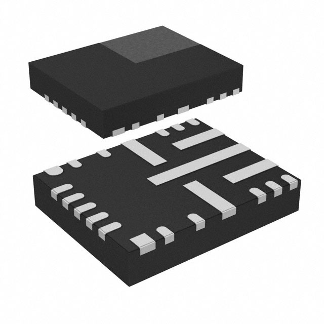


 工商网监
湘ICP备2023018690号
工商网监
湘ICP备2023018690号
