LM9076
www.ti.com
SNVS260L – NOVEMEBER 2003 – REVISED MARCH 2013
LM9076 150mA Ultra-Low Quiescent Current LDO Regulator with Delayed Reset Output
Check for Samples: LM9076
FEATURES
DESCRIPTION
•
•
The LM9076 is a ±3%, 150 mA logic controlled
voltage regulator. The regulator features an active
low delayed reset output flag which can be used to
reset a microprocessor system at turn-ON and in the
event that the regulator output voltage falls below a
minimum value. An external capacitor programs a
delay time interval before the reset output pin can
return high.
1
2
•
•
•
•
•
•
•
Available with 5.0V or 3.3V Output Voltage
Ultra Low Ground Pin Current, 25 μA Typical
for 100 μA Load
VOUT Initial Accuracy of ±1.5%
VOUT Accurate to ±3% Over Load and
Temperature Conditions
Low Dropout Voltage, 200 mV Typical with 150
mA Load
Low Off State Ground Pin current for
LM9076BMA
Delayed RESET Output Pin for Low VOUT
Detection
+70V/-50V Voltage Transients
Operational VIN up to +40V
Designed for automotive and industrial applications,
the LM9076 contains a variety of protection features
such as thermal shutdown, input transient protection
and a wide operating temperature range. The
LM9076 uses an PNP pass transistor which allows
low drop-out voltage operation.
Typical Applications
Unregulated
Voltage Input
VIN
Regulated
Voltage Output
VOUT
LM9076S-x.x
100 k:
Delayed Reset
Output
RESET
CDELAY
CIN
GND
0.1 PF
COUT
1.0 nF
10 PF
10 PF
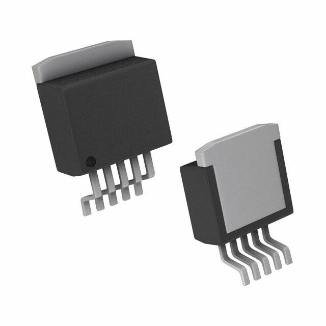
Figure 1. LM9076S-x.x in 5 lead SFM package
Unregulated
Voltage Input
VIN
Regulated
Voltage Output
VOUT
LM9076BMA-x.x
Shutdown Control
Input
ON
100 k:
Delayed Reset
Output
RESET
SHUTDOWN
OFF
CDELAY
CIN
0.1 PF
10 PF
GND
COUT
1.0 nF
10 PF
Figure 2. LM9076BMA-x.x in 8 lead SOIC package
1
2
Please be aware that an important notice concerning availability, standard warranty, and use in critical applications of
Texas Instruments semiconductor products and disclaimers thereto appears at the end of this data sheet.
All trademarks are the property of their respective owners.
PRODUCTION DATA information is current as of publication date.
Products conform to specifications per the terms of the Texas
Instruments standard warranty. Production processing does not
necessarily include testing of all parameters.
Copyright © 2003–2013, Texas Instruments Incorporated
�LM9076
SNVS260L – NOVEMEBER 2003 – REVISED MARCH 2013
www.ti.com
Connection Diagram
Figure 3. Top View
Part Numbers LM9076S-3.3 and LM9076S-5.0
See SFM Package Number KTT0005B
Figure 4. Top View
Part Numbers LM9076BMA-3.3 and
LM9076BMA-5.0
See SOIC Package Number D
These devices have limited built-in ESD protection. The leads should be shorted together or the device placed in conductive foam
during storage or handling to prevent electrostatic damage to the MOS gates.
Absolute Maximum Ratings (1)
VIN(DC)
-15V to +55V
VIN(+Transient) t< 10ms, Duty Cycle VOR to
RESET pin HIGH
SHUTDOWN CONTROL LOGIC — LM9076BMA-5.0 Only
VIL(SD)
SHUTDOWN Pin Low
Threshold Voltage
VSHUTDOWN pin falling
from 5.0V until VOUT
>4.5V (VOUT = On)
1
1.5
–
V
VIH(SD)
SHUTDOWN Pin High
Threshold Voltage
VSHUTDOWN pin rising
from 0V until VOUT <
0.5V (VOUT = Off)
–
1.5
2
V
VSHUTDOWN = 40V
–
35
–
μA
IIH(SD)
SHUTDOWN Pin High
Bias Current
VSHUTDOWN = 5V
–
15
35
μA
VSHUTDOWN = 2V
–
6
10
μA
VSHUTDOWN = 0V
–
0
–
μA
IIL(SD)
SHUTDOWN Pin Low
Bias Current
Submit Documentation Feedback
Copyright © 2003–2013, Texas Instruments Incorporated
Product Folder Links: LM9076
5
�LM9076
SNVS260L – NOVEMEBER 2003 – REVISED MARCH 2013
www.ti.com
Typical Performance Characteristics
6
Output Capacitor ESR
Output Capacitor ESR
Figure 5.
Figure 6.
Output Voltage vs Low Input Voltage
Output Voltage vs Low Input Voltage
Figure 7.
Figure 8.
Ground Pin Current vs Low Input Voltage
Ground Pin Current vs Low Input Voltage
Figure 9.
Figure 10.
Submit Documentation Feedback
Copyright © 2003–2013, Texas Instruments Incorporated
Product Folder Links: LM9076
�LM9076
www.ti.com
SNVS260L – NOVEMEBER 2003 – REVISED MARCH 2013
Typical Performance Characteristics (continued)
Ground Pin Current vs Load Current
Ground Pin Current vs Load Current
Figure 11.
Figure 12.
Output Voltage vs Input Voltage
Output Voltage vs Input Voltage
Figure 13.
Figure 14.
Output Voltage vs Junction Temperature
Output Voltage vs Junction Temperature
Figure 15.
Figure 16.
Submit Documentation Feedback
Copyright © 2003–2013, Texas Instruments Incorporated
Product Folder Links: LM9076
7
�LM9076
SNVS260L – NOVEMEBER 2003 – REVISED MARCH 2013
www.ti.com
Typical Performance Characteristics (continued)
8
Dropout Voltage vs Load Current
Load Transient Response
Figure 17.
Figure 18.
Load Transient Response
Line Transient Response
Figure 19.
Figure 20.
Line Transient Response
Delayed Reset Time vs Vin
Normalized to VIN = 14V
Figure 21.
Figure 22.
Submit Documentation Feedback
Copyright © 2003–2013, Texas Instruments Incorporated
Product Folder Links: LM9076
�LM9076
www.ti.com
SNVS260L – NOVEMEBER 2003 – REVISED MARCH 2013
Typical Performance Characteristics (continued)
Ripple Rejection
Figure 23.
Submit Documentation Feedback
Copyright © 2003–2013, Texas Instruments Incorporated
Product Folder Links: LM9076
9
�LM9076
SNVS260L – NOVEMEBER 2003 – REVISED MARCH 2013
www.ti.com
APPLICATION INFORMATION
REGULATOR BASICS
The LM9076 regulator is suitable for Automotive and Industrial applications where continuous connection to a
battery supply is required (refer to Typical Applications).
The pass element of the regulator is a PNP device which requires an output bypass capacitor for stability. The
minimum bypass capacitance for the output is 10 μF (refer to ESR limitations). A 22 μF, or larger, output bypass
capacitor is recommended for typical applications
INPUT CAPACITOR
The LM9076 requires a low source impedance to maintain regulator stability because critical portions of the
internal bias circuitry are connected to directly to VIN. In general, a 10 μF electrolytic capacitor, located within two
inches of the LM9076, is adequate for a majority of applications. Additionally, and at a minimum, a 0.1 μF
ceramic capacitor should be located between the LM9076 VIN and Ground pin, and as close as is physically
possible to the LM9076 itself .
OUTPUT CAPACITOR
An output bypass capacitor is required for stability. This capacitance must be placed between the LM9076 VOUT
pin and Ground pin, as close as is physically possible, using traces that are not part of the load current path.
The output capacitor must meet the requirements for minimum capacitance and also maintain the appropriate
ESR value across the entire operating ambient temperature range. There is no limit to the maximum output
capacitance as long as ESR is maintained.
The minimum bypass capacitance for the output is 10 μF (refer to ESR limitations). A 22 μF, or larger, output
bypass capacitor is recommended for typical applications.
Solid tantalums capacitors are recommended as they generally maintain capacitance and ESR ratings over a
wide temperature range. Ceramic capacitor types XR7 and XR5 may be used if a series resistor is added to
simulate the minimum ESR requirement. See Figure 24.
Aluminum electrolytic capacitors are not recommended as they are subject to wide changes in capacitance and
ESR across temperature.
Figure 24. Using Low ESR Capacitors
DELAY CAPACITOR
The capacitor on the Delay pin must be a low leakage type since the charge current is minimal (420 nA typical)
and the pin must fully charge to VOUT. Ceramic, Mylar, and polystyrene capacitor types are generally
recommended, although changes in capacitance values across temperature changes will have some effect on
the delay timing.
Any leakage of the IDELAY current, be it through the delay capacitor or any other path, will extend the delay time,
possibly to the point that the Reset pin output does not go high.
SHUTDOWN PIN - LM9076BMA ONLY
The basic On/Off control of the regulator is accomplished with the SHUTDOWN pin. By pulling the SHUTDOWN
pin high the regulator output is switched Off. When the regulator is switched Off the load on the battery will be
primarily due to the SHUTDOWN pin current.
10
Submit Documentation Feedback
Copyright © 2003–2013, Texas Instruments Incorporated
Product Folder Links: LM9076
�LM9076
www.ti.com
SNVS260L – NOVEMEBER 2003 – REVISED MARCH 2013
When the SHUTDOWN pin is low, or left open, the regulator is switched On. When an unregulated supply, such
as V BATTERY , is used to pull the SHUTDOWN pin high a series resistor in the range of 10KΩ to 50KΩ is
recommended to provide reverse voltage transient protection of the SHUTDOWN pin. Adding a small capacitor
(0.001uF typical) from the SHUTDOWN pin to Ground will add noise immunity to prevent accidental turn on due
to noise on the supply line.
RESET FLAG
The RESET pin is an open collector output which requires an external pull-up resistor to develop the reset signal.
The external pull-up resistor should be in the range of 10 kΩ to 200 kΩ.
At VIN values of less than typically 2V the RESET pin voltage will be high. For VIN values between typically 2V
and approximately VOUT + VBE the RESET pin voltage will be low. For VIN values greater than approximately
VOUT + VBE the RESET pin voltage will be dependent on the status of the VOUT pin voltage and the Delayed
Reset circuitry. The value of VBE is typically 600 mV at 25°C and will decrease approximately 2 mV for every 1°C
increase in the junction temperature. During normal operation the RESET pin voltage will be high .
Any load condition that causes the VOUT pin voltage to drop below typically 89% of normal will activate the
Delayed Reset circuit and the RESET pin will go low for the duration of the delay time.
Any line condition that causes VIN pin voltage to drop below typically VOUT + VBE will cause the RESET pin to go
low without activating the Delayed Reset circuitry.
Excessive thermal dissipation will raise the junction temperature and could activate the Thermal Shutdown
circuitry which, in turn, will cause the RESET pin to go low.
For the LM9076BMA devices, pulling the SHUTDOWN pin high will turn off the output which, in turn, will cause
the RESET pin to go low once the VOUT voltage has decayed to a value that is less than typically 89% of normal.
See Figure 25.
RESET DELAY TIME
When the regulator output is switched On, or after recovery from brief VOUT fault condition, the RESET flag can
be can be programmed to remain low for an additional delay time. This will give time for any system reference
voltages, clock signals, etc., to stabilize before the micro-controller resumes normal operation.
This delay time is controlled by the capacitor value on the CDELAY pin. During normal operation the CDELAY
capacitor is charged to near VOUT . When a VOUT fault causes the RESET pin to go low, the CDELAY capacitor is
quickly discharged to ground. When the VOUT fault is removed, and VOUT returns to the normal operating value,
the CDELAY capacitor begins charging at a typical constant 0.420 uA rate. When the voltage on the CDELAY
capacitor reaches the same potential as the VOUT pin the RESET pin will be allowed to return high.
The typical RESET delay time can be calculated with the following formula:
tDELAY = VOUT X (CDELAY / IDELAY )
(1)
For the LM9076–3.3 with a CDELAY value of 0.001 uF and a IDELAY value of 0.420 uA the typical RESET delay
time is:
tDELAY =3.3V × (0.001 uF / 0.420 uA) = 7.8 ms
(2)
For the LM9076–5.0 with a CDELAY value of 0.001 uF and a IDELAY value of 0.420 uA the typical RESET delay
time is:
tDELAY = 5.0V X (0.001uF / 0.420uA) = 11.9 ms
(3)
Submit Documentation Feedback
Copyright © 2003–2013, Texas Instruments Incorporated
Product Folder Links: LM9076
11
�LM9076
SNVS260L – NOVEMEBER 2003 – REVISED MARCH 2013
www.ti.com
THERMAL PROTECTION
Device operational range is limited by the maximum junction temperature (TJ). The junction temperature is
influenced by the ambient temperature (TA), package selection, input voltage (VIN), and the output load current.
When operating with maximum load currents the input voltage and/or ambient temperature will be limited. When
operating with maximum input voltage the load current and/or the ambient temperature will be limited.
Even though the LM9076 is equipped with circuitry to protect itself from excessive thermal dissipation, it is not
recommended that the LM9076 be operated at, or near, the maximum recommended die junction temperature
(TJ) as this may impair long term device reliability.
The thermal protection circuity monitors the temperature at the die level. When the die temperature exceeds
typically 160°C the voltage regulator output will be switched off.
Figure 25. Typical Reset Pin Operational Waveforms
12
Submit Documentation Feedback
Copyright © 2003–2013, Texas Instruments Incorporated
Product Folder Links: LM9076
�LM9076
www.ti.com
SNVS260L – NOVEMEBER 2003 – REVISED MARCH 2013
REVISION HISTORY
Changes from Revision K (March 2013) to Revision L
•
Page
Changed layout of National Data Sheet to TI format .......................................................................................................... 12
Submit Documentation Feedback
Copyright © 2003–2013, Texas Instruments Incorporated
Product Folder Links: LM9076
13
�PACKAGE OPTION ADDENDUM
www.ti.com
30-Sep-2021
PACKAGING INFORMATION
Orderable Device
Status
(1)
Package Type Package Pins Package
Drawing
Qty
Eco Plan
(2)
Lead finish/
Ball material
MSL Peak Temp
Op Temp (°C)
Device Marking
(3)
(4/5)
(6)
LM9076BMA-3.3/NOPB
ACTIVE
SOIC
D
8
95
RoHS & Green
SN
Level-1-260C-UNLIM
-40 to 125
9076B
MA3.3
LM9076BMA-5.0
NRND
SOIC
D
8
95
Non-RoHS
& Green
Call TI
Level-1-235C-UNLIM
-40 to 125
9076B
MA5.0
LM9076BMA-5.0/NOPB
ACTIVE
SOIC
D
8
95
RoHS & Green
SN
Level-1-260C-UNLIM
-40 to 125
9076B
MA5.0
LM9076BMAX-3.3/NOPB
ACTIVE
SOIC
D
8
2500
RoHS & Green
SN
Level-1-260C-UNLIM
-40 to 125
9076B
MA3.3
LM9076BMAX-5.0/NOPB
ACTIVE
SOIC
D
8
2500
RoHS & Green
SN
Level-1-260C-UNLIM
-40 to 125
9076B
MA5.0
LM9076S-3.3/NOPB
ACTIVE
DDPAK/
TO-263
KTT
5
45
RoHS-Exempt
& Green
SN
Level-3-245C-168 HR
-40 to 125
LM9076S
-3.3
LM9076S-5.0
NRND
DDPAK/
TO-263
KTT
5
45
Non-RoHS
& Green
Call TI
Level-3-235C-168 HR
-40 to 125
LM9076S
-5.0
LM9076S-5.0/NOPB
ACTIVE
DDPAK/
TO-263
KTT
5
45
RoHS-Exempt
& Green
SN
Level-3-245C-168 HR
-40 to 125
LM9076S
-5.0
LM9076SX-3.3/NOPB
ACTIVE
DDPAK/
TO-263
KTT
5
500
RoHS-Exempt
& Green
SN
Level-3-245C-168 HR
-40 to 125
LM9076S
-3.3
LM9076SX-5.0/NOPB
ACTIVE
DDPAK/
TO-263
KTT
5
500
RoHS-Exempt
& Green
SN
Level-3-245C-168 HR
-40 to 125
LM9076S
-5.0
(1)
The marketing status values are defined as follows:
ACTIVE: Product device recommended for new designs.
LIFEBUY: TI has announced that the device will be discontinued, and a lifetime-buy period is in effect.
NRND: Not recommended for new designs. Device is in production to support existing customers, but TI does not recommend using this part in a new design.
PREVIEW: Device has been announced but is not in production. Samples may or may not be available.
OBSOLETE: TI has discontinued the production of the device.
(2)
RoHS: TI defines "RoHS" to mean semiconductor products that are compliant with the current EU RoHS requirements for all 10 RoHS substances, including the requirement that RoHS substance
do not exceed 0.1% by weight in homogeneous materials. Where designed to be soldered at high temperatures, "RoHS" products are suitable for use in specified lead-free processes. TI may
reference these types of products as "Pb-Free".
RoHS Exempt: TI defines "RoHS Exempt" to mean products that contain lead but are compliant with EU RoHS pursuant to a specific EU RoHS exemption.
Green: TI defines "Green" to mean the content of Chlorine (Cl) and Bromine (Br) based flame retardants meet JS709B low halogen requirements of


 工商网监
湘ICP备2023018690号
工商网监
湘ICP备2023018690号
