LM95233
Dual Remote Diode and Local Temperature Sensor with
SMBus Interface and TruTherm™ Technology
General Description
LM95233 is an 11-bit digital temperature sensor with a 2-wire
System Management Bus (SMBus) interface that can monitor
the temperature of two remote diodes as well as its own temperature. The LM95233 can be used to very accurately monitor the temperature of up to two external devices such as
microprocessors, graphics processors or diode-connected
2N3904s. The LM95233's TruTherm™ BJT beta compensation technology allows sensing of 90nm or 65nm process
thermal diodes accurately.
The LM95233 reports temperature in two different formats for
+127.875°C/–128°C range and 0°C/255°C range. The
LM95233 TCRIT1, TCRIT2 and TCRIT3 outputs are triggered
when any unmasked channel exceeds its corresponding programmable limit and can be used to shutdown the system, to
turn on the system fans or as a microcontroller interrupt function. The current status of the TCRIT1, TCRIT2 and TCRIT3
pins can be read back from the status registers. Mask registers are available for further control of the TCRIT outputs.
LM95233's remote temperature channels have programmable digital filters to minimize unwanted TCRIT events
when temperature spikes are encountered.
For optimum flexibility and accuracy each LM95233 channel
includes, registers for sub-micron process or 2N3904 diode
model selection as well as offset correction. A three level address pin allows connection of up to 3 LM95233s to the same
SMBus master. The LM95233 includes power saving functions such as: programmable conversion rate, shutdown
mode, and turn off of unused channels.
■ 0.125°C LSb temperature resolution
■ 0.03125°C LSb remote temperature resolution with digital
filter enabled
■ +127.875°C/–128°C and 0°C/255°C remote ranges
■ Programmable digital filters and analog front end filter
■ Remote diode fault detection, model selection and offset
correction
■ Mask and status register support
■ 3 programmable TCRIT outputs with programmable
shared hysteresis
■ Programmable conversion rate and shutdown mode oneshot conversion control
■ SMBus 2.0 compatible interface, supports TIMEOUT
■ Three-level address pin
■ 14-pin LLP package
Key Specifications
±2.0 °C (max)
■ Local Temperature Accuracy
■ Remote Diode Temperature Accuracy ±0.875 °C (max)
3.0 V to 3.6 V
■ Supply Voltage
0.57 mA (typ)
■ Average Supply Current (1Hz
conversion rate)
Applications
■ Processor/Computer System Thermal Management
(e.g. Laptop, Desktop, Workstations, Server)
■ Electronic Test Equipment
■ Office Electronics
Features
■ Accurately senses die temperature of 2 remote ICs or
diode junctions and local temperature
■ TruTherm BJT beta compensation technology accurately
senses sub-micron process thermal diodes
Connection Diagram
LLP-14
20206301
TOP VIEW
TruTherm™ is a trademark of National Semiconductor Corporation.
Intel™ is a trademark of Intel Corporation.
Pentium™ is a trademark of Intel Corporation.
© 2011 National Semiconductor Corporation
202063
www.national.com
LM95233 Dual Remote Diode and Local Temperature Sensor with SMBus Interface and TruTherm
Technology
April 1, 2011
�LM95233
Ordering Information
Package
Marking
NS Package
Number
Transport
Media
LM95233CISD
95233CI
SDA14B (LLP-14)
1000 Units on Tape and Reel
LM95233CISDX
95233CI
SDA14B (LLP-14)
4500 Units on Tape and Reel
Part Number
Simplified Block Diagram
20206302
Pin Descriptions
Label
Pin #
NC
1
No Connect
Not connected. May be left floating, connected to GND or
VDD.
VDD
2
Positive Supply Voltage Input
DC Voltage from 3.0 V to 3.6 V. VDD should be bypassed with
a 0.1µF capacitor in parallel with 100pF. The 100pF capacitor
should be placed as close as possible to the power supply
pin. Noise should be kept below 200 mVp-p, a 10 µF capacitor
may be required to achieve this.
NC
3
No Connect
Not connected. May be left floating, connected to GND or
VDD.
NC
4
No Connect
Not connected. May be left floating, connected to GND or
VDD.
D−
5
Diode Return Current Sink
To all Diode Cathodes. Common D- pin for all two remote
diodes.
www.national.com
Function
Typical Connection
2
�Pin #
Function
Typical Connection
D2+
6
Diode Current Source
To second Diode Anode. Connected to remote discrete diodeconnected transistor junction or to the diode-connected
transistor junction on a remote IC whose die temperature is
being sensed. A capacitor is not required between D2+ and
D-. A 100 pF capacitor between D2+ and D- can be added
and may improve perfomance in noisy systems. Float this pin
if this thermal diode is not used.
D1+
7
Diode Current Source
To first Diode Anode. Connected to remote discrete diodeconnected transistor junction or to the diode-connected
transistor junction on a remote IC whose die temperature is
being sensed. A capacitor is not required between D1+ and
D-. A 100 pF capacitor between D1+ and D- can be added
and may improve perfomance in noisy systems. Float this pin
if this thermal diode is not used.
GND
8
Power Supply Ground
System low noise ground.
A0
9
Dgital Input
SMBus slave address select pin. Selects one of three
addresses. Can be tied to VDD, GND, or to the middle of a
resistor divider connected between VDD and GND.
TCRIT1
10
Digital Output, Open-Drain
Critical temperature output 1. Requires pull-up resistor. Active
"LOW".
TCRIT2
11
Digital Output, Open-Drain
Critical temperature output 2. Requires pull-up resistor. Active
"LOW".
SMBDAT
12
SMBus Bi-Directional Data
Line, Open-Drain Output
From and to Controller; may require an external pull-up
resistor
SMBCLK
13
SMBus Clock Input
From Controller; may require an external pull-up resistor
TCRIT3
14
Digital Output, Open-Drain
Critical temperature output 3. Requires pull-up resistor. Active
"LOW".
N/A
N/A
Thermal pad
Connect the thermal pad to GND.
3
www.national.com
LM95233
Label
�LM95233
Typical Application
20206303
www.national.com
4
�Supply Voltage
−0.3V to 6.0V
Voltage at SMBDAT, SMBCLK,
TCRIT1, TCRIT2, TCRIT3
−0.5V to 6.0V
Voltage at Other Pins
−0.3V to (VDD + 0.3V)
D− Input Current
±1 mA
Input Current at All Other Pins (Note 2)
±5 mA
Package Input Current (Note 2)
30 mA
SMBDAT, TCRIT1, TCRIT2,
TCRIT3 Output Sink Current
10 mA
Storage Temperature
−65°C to +150°C
ESD Susceptibility (Note 4)
Human Body Model
2000V
Machine Model
200V
Operating Ratings
(Note 1, Note 5)
Operating Temperature Range
Electrical Characteristics Temperature
Range
LM95233CISD
−40°C to +140°C
TMIN ≤ TA ≤ TMAX
Supply Voltage Range (VDD)
−40°C ≤ TA ≤
+125°C
+3.0V to +3.6V
Temperature-to-Digital Converter Electrical Characteristics
Unless otherwise noted, these specifications apply for VDD = +3.0Vdc to 3.6Vdc. Boldface limits apply for TA = TJ = TMIN ≤ TA
≤ TMAX; all other limits TA = TJ = +25°C, unless otherwise noted.
Parameter
Typical
(Note 6)
Conditions
Units
(Limit)
Temperature Error Using Local Diode
TA = -40°C to +125°C, (Note 8)
±2
°C (max)
Temperature Error Using Remote Diode (Note
9)
TA = +25°C to +85°C
TD = +60°C to +100°C
65 nm Intel
Processor
±0.875
°C (max)
TA = +25°C to +85°C
TD = +60°C to +100°C
MMBT3904
Transistor
±1.1
°C (max)
TA = +25°C to +85°C
TD = 40°C to +125°C
65 nm Intel
Processor
±1.0
°C (max)
TA = +25°C to +85°C
TD = −40°C to +125°C
MMBT3904
Transistor
±1.3
°C (max)
TA = −40°C to +85°C
TD = −40°C to +125°C
65 nm Intel
Processor
±3.2
°C (max)
TA = −40°C to +85°C
TD = −40°C to +125°C
MMBT3904
Transistor
±3.0
°C (max)
TA = −40°C to +85°C
TD = 125°C to +140°C
MMBT3904
Transistor
±3.3
°C (max)
Local Diode Measurement Resolution
Remote Diode Measurement Resolution
11
Digital Filter Off
Digital Filter On (Remote Diodes 1 and 2
only)
Conversion Time of All Temperatures at the
Fastest Setting (Note 11)
Quiescent Current (Note 10)
Bits
0.125
°C
11
Bits
0.125
°C
13
Bits
0.03125
°C
All Channels are Enabled in Default
State
1100
1210
ms (max)
1 External Channel TruTherm Active
34
37
ms (max)
1 External Channel TruTherm Inactive
31
34
ms (max)
Local only
30
33
ms (max)
SMBus Inactive, 1Hz Conversion Rate,
channels in default state
570
800
µA (max)
Shutdown
360
High level
160
Low level
10
D− Source Voltage
Remote Diode Source Current
±1
Limits
(Note 7)
µA
0.4
5
V
230
µA (max)
www.national.com
LM95233
Charge Device Model
1000V
Soldering process must comply with National’s reflow
temperature profile specifications. Refer to http://
www.national.com/packaging/. (Note 3)
Absolute Maximum Ratings (Note 1)
�LM95233
Parameter
Conditions
Typical
(Note 6)
Limits
(Note 7)
Units
(Limit)
2.8
1.6
V (max)
V (min)
Power-On Reset Threshold
Measured on VDD input, falling edge
TCRIT1 Pin Temperature Threshold
Default Diodes only
+110
°C
TCRIT2 Pin Temperature Threshold
Default all channels
+85
°C
Logic Electrical Characteristics
DIGITAL DC CHARACTERISTICS
Unless otherwise noted, these specifications apply for VDD = +3.0Vdc to 3.6Vdc. Boldface limits apply for TA = TJ = TMIN to
TMAX; all other limits TA= TJ=+25°C, unless otherwise noted.
Symbol
Parameter
Conditions
Typical
(Note 6)
Limits
(Note 7)
Units
(Limit)
SMBDAT, SMBCLK INPUTS
VIN(1)
Logical “1” Input Voltage
2.1
V (min)
VIN(0)
Logical “0”Input Voltage
0.8
V (max)
VIN(HYST)
SMBDAT and SMBCLK Digital Input Hysteresis
400
mV
IIN(1)
Logical “1” Input Current
VIN = VDD
0.005
10
µA (max)
IIN(0)
Logical “0” Input Current
VIN = 0V
−0.005
-10
µA (max)
CIN
Input Capacitance
5
pF
A0 DIGITAL INPUT
VIH
Input High Voltage
0.90 × VDD
V (min)
VIM
Input Middle Voltage
0.57 × VDD
V (max)
0.43 × VDD
V (min)
0.10 × VDD
V (max)
IIN(1)
VIL
Input Low Voltage
Logical "1" Input Current
VIN = VDD
−0.005
−10
µA (min)
IIN(0)
Logical "0" Input Current
VIN = 0V
0.005
10
µA (max)
CIN
Input Capacitance
5
pF
SMBDAT, TCRIT1, TCRIT2, TCRIT3 DIGITAL OUTPUTS
IOH
High Level Output Current
VOL(SMBDAT) SMBus Low Level Output Voltage
VOL(TCRIT)
COUT
TCRIT1, TCRIT2, TCRIT3 Low Level Output
Voltage
VOH = VDD
10
µA (max)
IOL = 4 mA
IOL = 6 mA
0.4
0.6
V (max)
V (max)
IOL= 6 mA
0.4
V (max)
Digital Output Capacitance
www.national.com
5
6
pF
�Unless otherwise noted, these specifications apply for VDD=+3.0 Vdc to +3.6 Vdc, CL (load capacitance) on output lines = 80 pF.
Boldface limits apply for TA = TJ = TMIN to TMAX; all other limits TA = TJ = +25°C, unless otherwise noted.
The switching characteristics of the LM95233 fully meet or exceed the published specifications of the SMBus version 2.0. The
following parameters are the timing relationships between SMBCLK and SMBDAT signals related to the LM95233. They adhere
to but are not necessarily the SMBus bus specifications.
Symbol
Parameter
Conditions
Typical
(Note 6)
Limits
(Note 7)
Units
(Limit)
100
10
kHz (max)
kHz (min)
fSMB
SMBus Clock Frequency
tLOW
SMBus Clock Low Time
from VIN(0)max to VIN(0)max
4.7
25
µs (min)
ms (max)
tHIGH
SMBus Clock High Time
from VIN(1)min to VIN(1)min
4.0
µs (min)
tR,SMB
SMBus Rise Time
(Note 12)
1
µs (max)
tF,SMB
SMBus Fall Time
(Note 13)
0.3
µs (max)
tOF
Output Fall Time
CL = 400 pF,
IO = 3 mA, (Note 13)
250
ns (max)
tTIMEOUT
SMBDAT and SMBCLK Time Low for Reset of
Serial Interface (Note 14)
25
35
ms (min)
ms (max)
tSU;DAT
Data In Setup Time to SMBCLK High
250
ns (min)
tHD;DAT
Data Out Stable after SMBCLK Low
300
1075
ns (min)
ns (max)
tHD;STA
Start Condition SMBDAT Low to SMBCLK Low
(Start condition hold before the first clock falling
edge)
100
ns (min)
tSU;STO
Stop Condition SMBCLK High to SMBDAT Low
(Stop Condition Setup)
100
ns (min)
tSU;STA
SMBus Repeated Start-Condition Setup Time,
SMBCLK High to SMBDAT Low
0.6
µs (min)
SMBus Free Time Between Stop and Start
Conditions
1.3
µs (min)
tBUF
SMBus Communication
20206309
Note 1: Absolute Maximum Ratings indicate limits beyond which damage to the device may occur. DC and AC electrical specifications do not apply when operating
the device beyond its rated operating conditions.
Note 2: When the input voltage (VI) at any pin exceeds the power supplies (VI < GND or VI > VDD), the current at that pin should be limited to 5 mA.
Parasitic components and or ESD protection circuitry are shown in the table below for the LM95233's pins.
7
www.national.com
LM95233
SMBus DIGITAL SWITCHING CHARACTERISTICS
�LM95233
Pin #
Label
Circuit
1
NC
–
2
VDD
A
3
NC
–
4
NC
–
5
D-
A
6
D2+
A
7
D1+
A
8
GND
–
Circuits for Pin ESD Protection Structure
Circuit A
9
A0
B
10
TCRIT1
B
11
TCRIT2
B
12
SMBDAT
B
13
SMBCLK
B
14
TCRIT2
B
Circuit B
Note 3: Reflow temperature profiles are different for packages containing lead (Pb) than for those that do not.
Note 4: Human body model, 100 pF discharged through a 1.5 kΩ resistor. Machine model, 200 pF discharged directly into each pin. Charged Device Model
(CDM) simulates a pin slowly acquiring charge (such as from a device sliding down the feeder in an automated assembler) then rapidly being discharged.
Note 5: Thermal resistance junction-to-ambient when attached to a 4 layer printed circuit board per JEDEC standard JESD51-7:
– 14-lead LLP = 90°C/W (no thermal vias, no airflow)
– 14-lead LLP = 63°C/W (1 thermal via, no airflow)
– 14-lead LLP = 43°C/W (6 thermal vias, no airflow)
– 14-lead LLP = 31°C/W (6 thermal vias, 900 ln. ft. / min. airflow)
Note, all quoted values include +15% error factor from nominal value.
Note 6: Typicals are at TA = 25°C and represent most likely parametric norm.
Note 7: Limits are guaranteed to National's AOQL (Average Outgoing Quality Level).
Note 8: Local temperature accuracy does not include the effects of self-heating. The rise in temperature due to self-heating is the product of the internal power
dissipation of the LM95233 and the thermal resistance. See (Note 5) for the thermal resistance to be used in the self-heating calculation.
Note 9: The accuracy of the LM95233CISD is guaranteed when using a typical thermal diode of an Intel processor on a 65 nm process or an MMBT3904 diodeconnected transistor, as selected in the Remote Diode Model Select register. See typical performance curve for performance with Intel processor on a 90 nm
process. For further information on other thermal diodes see applications Section 3.1 "Diode Non-ideality" or send email to hardware.monitor.team@national.com.
Note 10: Quiescent current will not increase substantially with an SMBus communication.
Note 11: This specification is provided only to indicate how often temperature data is updated. The LM95233 can be read at any time without regard to conversion
state (and will yield last conversion result).
Note 12: The output rise time is measured from (VIN(0)max − 0.15V) to (VIN(1)min + 0.15V).
Note 13: The output fall time is measured from (VIN(1)min + 0.15V) to (VIN(0)max − 0.15V).
Note 14: Holding the SMBDAT and/or SMBCLK lines Low for a time interval greater than tTIMEOUT will reset the LM95233's SMBus state machine, therefore setting
SMBDAT and SMBCLK pins to a high impedance state.
www.national.com
8
�LM95233
Typical Performance Characteristics
Conversion Rate Effect on
Average Power Supply Current
Thermal Diode Capacitor or PCB
Leakage Current Effect on
Remote Diode Temperature Reading
20206306
20206323
Remote Temperature Reading Sensitivity to
Thermal Diode Filter Capacitance,
TruTherm Disabled
Remote Temperature Reading Sensitivity to
Thermal Diode Filter Capacitance,
TruTherm Enabled
20206307
20206308
Intel Processor on 65 nm Process or 90 nm Process
Thermal Diode Performance Comparison
20206324
9
www.national.com
�LM95233
1.0 Functional Description
LM95233 is an 11-bit digital temperature sensor with a 2-wire
System Management Bus (SMBus) interface that can monitor
the temperature of two remote diodes as well as its own temperature. The LM95233 can be used to very accurately monitor the temperature of up to two external devices such as
microprocessors, graphics processors or diode-connected
2N3904 transistor. The LM95233 includes TruTherm BJT beta compensation technology that allows sensing of Intel processors 90 nm or 65 nm process thermal diodes accurately.
The LM95233 reports temperature in two different formats for
+127.875°C/–128°C range and 0°C/255°C range. The
LM95233 has a Sigma-Delta ADC (Analog-to-Digital Converter) core which provides the first level of noise imunity. For
improved performance in a noisy environment the LM95233
includes programmable digital filters for Remote Diode 1 and
2 temperature readings. When the digital filters are invoked
the resolution for Remote Diode 1 and 2 readings increases
to 0.03125°C. The LM95233 contains a diode model selection
register that includes bits for each channel that select between thermal diodes of Intel™ processors on 65 nm process
or 2N3904s. For maximum flexibility and best accuracy the
LM95233 includes offset registers that allow calibration of
other diode types.
Diode fault detection circuitry in the LM95233 can detect the
absence or fault state of a remote diode: whether D+ is shorted to VDD, D- or ground, or whether D+ is floating.
The LM95233 TCRIT1, TCRIT2 and TCRIT3 active low outputs are triggered when any unmasked channel exceeds its
corresponding programmable limit and can be used to shutdown the system, to turn on the system fans or as a microcontroller interrupt function. The current status of the
TCRIT1, TCRIT2 and TCRIT3 pins can be read back from the
status registers via the SMBus interface. The remote channels have two separate limits each that control the TCRIT1
and TCRIT2 pins. The TCRIT3 pin shares the limits of the
TCRIT2 pin but allows for different masking options. All limits
have a shared programmable hysteresis register.
Remote Diode temperature channels have programmable
digital filters in order to avoid false triggering the TCRIT pins.
LM95233 has a three-level address pin to connect up to 3
devices to the same SMBus master. LM95233 also has programmable conversion rate register as well as a shutdown
mode for power savings. One round of conversions can be
triggered in shutdown mode by writing to the one-shot register
through the SMBus interface. LM95233 can be programmed
to turn off unused channels for more power savings.
The LM95233 register set has an 8-bit data structure and includes:
1. Temperature Value Registers with signed format
— Most-Significant-Byte (MSB) and Least-SignificantByte (LSB) Local Temperature
— MSB and LSB Remote Temperature 1
— MSB and LSB Remote Temperature 2
2. Temperature Value Registers with unsigned format
— MSB and LSB Remote Temperature 1
— MSB and LSB Remote Temperature 2
3. Diode Configuration Registers
— Diode Model Select
— Remote 1 Offset
— Remote 2 Offset
4. General Configuration Registers
www.national.com
5.
6.
— Configuration (Standby, Conversion Rate)
— Channel Conversion Enable
— Filter Setting for Remote 1 and 2
— 1-Shot
Status Registers
— Main Status Register (Busy bit, Not Ready, Status
Register 1 to 4 Flags)
— Status 1 (diode fault)
— Status 2 (TCRIT1)
— Status 3 (TCRIT2)
— Status 4 (TCRIT3)
— Diode Model Status
Mask Registers
— TCRIT1 Mask
— TCRIT2 Mask
— TCRIT3 Mask
7.
Limit Registers
— Local Tcrit Limit
— Remote 1 Tcrit-1 Limit
— Remote 2 Tcrit-1 Limit
— Remote 1 Tcrit-2 and Tcrit-3 Limit
— Remote 2 Tcrit-2 and Tcrit-3 Limit
— Common Tcrit Hysteresis
8.
9.
Manufacturer ID Register
Revision ID Register
1.1 CONVERSION SEQUENCE
The LM95233 takes approximately 95 ms to convert the Local
Temperature, Remote Temperatures 1 and 2, and to update
all of its registers. These conversions for each thermal diode
are addressed in a round robin sequence. Only during the
conversion process the busy bit (D7) in Status register (02h)
is high. The conversion rate may be modified by the Conversion Rate bits found in the Configuration Register (03h).
When the conversion rate is modified a delay is inserted between each round of conversions, the actual time for each
round remains at 95 ms (typical all channels enabled). The
time a round takes depends on the number of channels that
are on. Different conversion rates will cause the LM95233 to
draw different amounts of average supply current as shown
in Figure 1. This curve assumes all the channels are on. If
channels are turned off the average current will drop since the
round robin time will decrease and the shutdown time will increase during each conversion interval.
10
�1.3 SMBus INTERFACE
The LM95233 operates as a slave on the SMBus, so the
SMBCLK line is an input and the SMBDAT line is bidirectional.
The LM95233 never drives the SMBCLK line and it does not
support clock stretching. According to SMBus specifications,
the LM95233 has a 7-bit slave address. Three SMBus device
address can be selected by connecting A0 (pin 6) to either
Low, Mid-Supply or High voltages. The LM95233 has the following SMBus slave address:
A0 Pin State
20206306
FIGURE 1. Conversion Rate Effect on Power Supply
Current
Remote 1
(°C)
Local
(°C)
TCRIT1
110
110
Masked,
85
TCRIT2
85
85
85
TCRIT3
Masked,
85
Masked,
85
Masked,
85
Binary
Low
18h
001 1000
Mid-Supply
2Ah
010 1010
High
2Bh
010 1011
1.5 DIGITAL FILTER
In order to suppress erroneous remote temperature readings
due to noise as well as increase the resolution of the temperature, the LM95233 incorporates a digital filter for Remote 1
and 2 Temperature Channels. When a filter is enabled the
filtered readings are used for the TCRIT comparisons. There
are two possible digital filter settings that are enabled through
the Filter Setting Register at register address 0Fh. The filter
for each channel can be set according to the following table:
R1F[1:0] or R2F[1:0]
Filter Setting
0
0
No Filter
0
1
Filter (equivalent to Level 2
filter of the LM86/LM89)
1
0
Reserved
1
1
Enhanced Filter (Filter with
transient noise clipping)
Temperature Channel Limit
Remote 2
(°C)
Hex
1.4 TEMPERATURE CONVERSION SEQUENCE
Each of the3 temperature channels of LM95233 can be turned
OFF independent from each other via the Channel Enable
Register. Turning off unused channels will increase the conversion speed in the fastest conversion speed mode. If the
slower conversion speed settings are used, disabling unused
channels will reduce the average power consumption of
LM95233.
1.2 POWER-ON-DEFAULT STATES
LM95233 always powers up to these known default states.
The LM95233 remains in these states until after the first conversion.
1. All Temperature readings set to 0°C until the end of the
first conversion
2. Diode Model Select: Remote 1 set to 65 nm Intel
processor, Remote 2 set to MMBT3904
3. Remote offset for all channels 0°C
4. Configuration: Active converting
5. Continuous conversion with all channels enabled,
time = 1s
6. Enhanced digital filter enabled for Remote 1 and 2
7. Status Registers depends on state of thermal diode
inputs
8. Local and Remote Temperature Limits for TCRIT1,
TCRIT2 and TCRIT3 outputs:
Output Pin
SMBus Device Address A[6:0]
Figure 2 describes the filter output in response to a step input
and an impulse input.
11
www.national.com
LM95233
9. Manufacturers ID set to 01h
10. Revision ID set to 79h
�LM95233
20206325
a) Seventeen and fifty degree step
response
20206326
b) Impulse response with input
transients less than 4°C
20206327
c) Impulse response with input
transients great than 4°C
FIGURE 2. Filter Impulse and Step Response Curves
11-bit, 2's Complement (10-bit plus sign)
Temperature
Digital Output
Binary
Hex
+125°C
0111 1101 0000 0000
7D00h
+25°C
0001 1001 0000 0000
1900h
+1°C
0000 0001 0000 0000
0100h
+0.125°C
0000 0000 0010 0000
0020h
0°C
0000 0000 0000 0000
0000h
−0.125°C
1111 1111 1110 0000
FFE0h
−1°C
1111 1111 0000 0000
FF00h
−25°C
1110 0111 0000 0000
E700h
−55°C
1100 1001 0000 0000
C900h
11-bit, Unsigned Binary
20206328
Temperature
FIGURE 3. Digital Filter Response in a typical Intel
processor on a 65 nm or 90 nm process. The filter curves
were purposely offset for clarity.
Digital Output
Binary
Hex
+255.875°C
1111 1111 1110 0000
FFE0h
+255°C
1111 1111 0000 0000
FF00h
Figure 3 shows the filter in use in a typical Intel processor on
a 65/90 nm process system. Note that the two curves have
been purposely offset for clarity. Inserting the filter does not
induce an offset as shown.
+201°C
1100 1001 0000 0000
C900h
+125°C
0111 1101 0000 0000
7D00h
+25°C
0001 1001 0000 0000
1900h
1.6 TEMPERATURE DATA FORMAT
Temperature data can only be read from the Local and Remote Temperature value registers. The data format for all
temperature values is left justified 16-bit word available in two
8-bit registers. Unused bits will always report "0". All temperature data is clamped and will not roll over when a temperature exceeds full-scale value.
Remote temperature data for all channels can be represented
by an 11-bit, two's complement word or unsigned binary word
with an LSb (Least Significant Bit) equal to 0.125°C.
+1°C
0000 0001 0000 0000
0100h
+0.125°C
0000 0000 0010 0000
0020h
0°C
0000 0000 0000 0000
0000h
www.national.com
When the digital filter is enabled on Remote 1 and 2 channels
temperature data is represented by a 13-bit unsigned binary
or 12-bit plus sign (two's complement) word with an LSb equal
to 0.03125°C.
12
�Temperature
Digital Output
Digital Output
Binary
Hex
Binary
Hex
−25°C
1110 0111 0000 0000
E700h
+125°C
0111 1101 0000 0000
7D00h
−55°C
1100 1001 0000 0000
C900h
+25°C
0001 1001 0000 0000
1900h
+1°C
0000 0001 0000 0000
0100h
+0.03125°C
0000 0000 0000 1000
0008h
0°C
0000 0000 0000 0000
0000h
−0.03125°C
1111 1111 1111 1000
FFF8h
−1°C
1111 1111 0000 0000
FF00h
−25°C
1110 0111 0000 0000
E700h
−55°C
1100 1001 0000 0000
C900h
1.7 SMBDAT OPEN-DRAIN OUTPUT
The SMBDAT output is an open-drain output and does not
have internal pull-ups. A “high” level will not be observed on
this pin until pull-up current is provided by some external
source, typically a pull-up resistor. Choice of resistor value
depends on many system factors but, in general, the pull-up
resistor should be as large as possible without effecting the
SMBus desired data rate. This will minimize any internal temperature reading errors due to internal heating of the
LM95233. The maximum resistance of the pull-up to provide
a 2.1V high level, based on LM95233 specification for High
Level Output Current with the supply voltage at 3.0V, is 82
kΩ (5%) or 88.7 kΩ (1%).
13-bit, Unsigned Binary
Temperature
Digital Output
Binary
Hex
+255.875°C
1111 1111 1110 0000
FFE0h
+255°C
1111 1111 0000 0000
FF00h
+201°C
1100 1001 0000 0000
C900h
+125°C
0111 1101 0000 0000
7D00h
+25°C
0001 1001 0000 0000
1900h
+1°C
0000 0001 0000 0000
0100h
+0.03125°C
0000 0000 0000 1000
0008h
0°C
0000 0000 0000 0000
0000h
1.8 TCRIT1, TCRIT2, AND TCRIT3 OUTPUTS
The LM95233's TCRIT pins are active-low open-drain outputs
and do not include internal pull-up resistors. A “high” level will
not be observed on these pins until pull-up current is provided
by some external source, typically a pull-up resistor. Choice
of resistor value depends on many system factors but, in general, the pull-up resistor should be as large as possible without
effecting the performance of the device receiving the signal.
This will minimize any internal temperature reading errors due
to internal heating of the LM95233. The maximum resistance
of the pull-up to provide a 2.1V high level, based on LM95233
specification for High Level Output Current with the supply
voltage at 3.0V, is 82 kΩ (5%) or 88.7 kΩ (1%). The three
TCRIT pins can each sink 6 mA of current and still guarantee
a "Logic Low" output voltage of 0.4V. If all three pins are set
at maximum current this will cause a power dissipation of 7.2
mW. This power dissipation combined with a thermal resistance of 77.8°C/W will cause the LM95233's junction temperature to rise approximately 0.6°C and thus cause the Local
temperature reading to shift. This can only be cancelled out if
the environment that the LM95233 is enclosed in has stable
and controlled air flow over the LM95233, as airflow can
cause the thermal resistance to change dramatically.
Local Temperature data is only represented by an 11-bit,
two's complement, word with an LSb equal to 0.125°C.
11-bit, 2's Complement (10-bit plus sign)
Temperature
Digital Output
Binary
Hex
+125°C
0111 1101 0000 0000
7D00h
+25°C
0001 1001 0000 0000
1900h
+1°C
0000 0001 0000 0000
0100h
+0.125°C
0000 0000 0010 0000
0020h
0°C
0000 0000 0000 0000
0000h
−0.125°C
1111 1111 1110 0000
FFE0h
−1°C
1111 1111 0000 0000
FF00h
1.9 TCRIT LIMITS AND TCRIT OUTPUTS
Figure 4 describes a simplified diagram of the temperature
comparison and status register logic. Figure 5 describes a
simplified logic diagram of the circuitry associated with the
status registers, mask registers and the TCRIT output pins.
13
www.national.com
LM95233
13-bit, 2's Complement (12-bit plus sign)
Temperature
�LM95233
20206350
FIGURE 4. Temperature Comparison Logic and Status Register Simplified Diagram
www.national.com
14
�LM95233
20206353
c) TCRIT3 Mask Register, Status Register 1 and 4, and
TCRIT3 output logic diagram.
20206351
a) TCRIT1 Mask Register, Status Register 1 and 2, and
TCRIT1 output logic diagram.
FIGURE 5. Logic diagrams for the TCRIT1, TCRIT2, and
TCRIT3 outputs.
If enabled, local temperature is compared to the user programmable Local Tcrit Limit Register (Default Value = 85°C).
The result of this comparison is stored in Status Register 2,
Status Register 3 and Status Register 4 (see Figure 4).The
comparison result can trigger TCRIT1 pin, TCRIT2 pin or
TCRIT3 pin depending on the settings in the TCRIT1 Mask,
TCRIT2 Mask and TCRIT3 Mask Registers (see Figure 5).
The comparison result can also be read back from the Status
Register 2, Status Register 3 and Status Register 4.
If enabled, remote temperature 1 is compared to the user
programmable Remote 1 Tcrit-1 Limit Register (Default Value
110°C) and Remote 1 Tcrit-2 Limit Register (Default Value =
85°C). The result of this comparison is stored in Status Register 2, Status Register 3 and Status Register 4 (see Figure
4). The comparison result can trigger TCRIT1 pin, TCRIT2 pin
or TCRIT3 pin depending on the settings in the TCRIT1 Mask,
TCRIT2 Mask and TRCIT3 Mask Registers (see Figure 5).
The comparison result can also be read back from the Status
Register 2, Status Register 3 and Status Register 4. The remote temperature 2 operates in a similar manner to remote
temperature 1 using its associated user programmable limit
registers: Remote 2 Tcrit-1 Limit Register (Default Value 110°
C) and Remote 2 Tcrit-2 Limit Register (Default Value = 85°
C).
Limit assignments for each TCRIT output pin:
TCRIT1
TCRIT2
TCRIT3
20206352
b) TCRIT2 Mask Register, Status Register 1 and 3, and
TCRIT2 output logic diagram.
15
Remote 2
Remote 2
Tcrit-1 Limit
Remote 2
Tcrit-2 Limit
Remote 2
Tcrit-2 Limit
Remote 1
Remote 1
Tcrit-1 Limit
Remote 1
Tcrit-2 Limit
Remote 1
Tcrit-2 Limit
Local
Local
Tcrit Limit
Local
Tcrit Limit
Local
Tcrit Limit
www.national.com
�LM95233
20206330
FIGURE 6. TCRIT response diagram (masking options not included)
The TCRIT response diagram of Figure 6 shows the local
temperature interaction with the Tcrit limit and hysteresis value. As can be seen in the diagram when the local temperature
exceeds the Tcrit limit register value the LTn Status bit is set
and the T_CRITn output(s) is/are activated. The Status bit(s)
and outputs are not deactivated until the temperature goes
below the value calculated by subtracting the Common Hysteresis value programmed from the limit. This diagram mainly
shows an example function of the hysteresis and is not meant
to show complete function of the possible settings and options
of all the TCRIT outputs and limit values.
A Write to the LM95233 will always include the address byte
and the command byte. A write to any register requires one
data byte.
Reading the LM95233 can take place either of two ways:
1. If the location latched in the Command Register is correct
(most of the time it is expected that the Command
Register will point to one of the Read Temperature
Registers because that will be the data most frequently
read from the LM95233), then the read can simply
consist of an address byte, followed by retrieving the data
byte.
2. If the Command Register needs to be set, then an
address byte, command byte, repeat start, and another
address byte will accomplish a read.
The data byte has the most significant bit first. At the end of
a read, the LM95233 can accept either acknowledge or No
Acknowledge from the Master (No Acknowledge is typically
used as a signal for the slave that the Master has read its last
byte). It takes the LM95233 95 ms (typical, all channels enabled) to measure the temperature of the remote diodes and
internal diode. When retrieving all 11 bits from a previous remote diode temperature measurement, the master must insure that all 11 bits are from the same temperature
conversion. This may be achieved by reading the MSB register first. The LSB will be locked after the MSB is read. The
LSB will be unlocked after being read. If the user reads MSBs
consecutively, each time the MSB is read, the LSB associated
with that temperature will be locked in and override the previous LSB value locked-in.
1.10 DIODE FAULT DETECTION
The LM95233 is equipped with operational circuitry designed
to detect fault conditions concerning the remote diodes. In the
event that the D+ pin is detected as shorted to GND, D−,
VDD or D+ is floating, the Remote Temperature reading
is –128.000 °C if signed format is selected and 0 °C if unsigned format is selected. In addition, the appropriate status
register bits RD1M or RD2M (D1 or D0) are set.
1.11 COMMUNICATING WITH THE LM95233
The data registers in the LM95233 are selected by the Command Register. At power-up the Command Register is set to
“00”, the location for the Read Local Temperature Register.
The Command Register latches the last location it was set to.
Each data register in the LM95233 falls into one of three types
of user accessibility:
1. Read only
2. Write only
3. Write/Read same address
www.national.com
16
�LM95233
20206310
(a) Serial Bus Write to the internal Command Register followed by a the Data Byte
20206311
(b) Serial Bus Write to the Internal Command Register
20206312
(c) Serial Bus Read from a Register with the Internal Command Register preset to desired value.
20206314
(d) Serial Bus Write followed by a Repeat Start and Immediate Read
FIGURE 7. SMBus Timing Diagrams
17
www.national.com
�LM95233
communication. After the start the LM95233 will expect
an SMBus Address address byte.
1.12 SERIAL INTERFACE RESET
In the event that the SMBus Master is RESET while the
LM95233 is transmitting on the SMBDAT line, the LM95233
must be returned to a known state in the communication protocol. This may be done in one of two ways:
1. When SMBDAT is LOW, the LM95233 SMBus state
machine resets to the SMBus idle state if either SMBDAT
or SMBCLK are held low for more than 35ms (tTIMEOUT).
Note that according to SMBus specification 2.0 all
devices are to timeout when either the SMBCLK or
SMBDAT lines are held low for 25-35ms. Therefore, to
insure a timeout of all devices on the bus the SMBCLK
or SMBDAT lines must be held low for at least 35ms.
2. When SMBDAT is HIGH, have the master initiate an
SMBus start. The LM95233 will respond properly to an
SMBus start condition at any point during the
1.13 ONE-SHOT CONVERSION
The One-Shot register is used to initiate a round of conversions and comparisons when the device is in standby mode,
after which the device returns to standby. This is not a data
register and it is the write operation that causes the one-shot
conversion. The data written to this address is irrelevant and
is not stored. A zero will always be read from this register. All
the channels that are enabled in the Channel Enable Register
will be converted once and the TCRIT1, TCRIT2 and
TCRIT3 pins will reflect the comparison results based on this
round of conversion results of the channels that are not
masked.
2.0 LM95233 Registers
Command register selects which registers will be read from or written to. Data for this register should be transmitted during the
Command Byte of the SMBus write communication.
P7
P6
P5
P4
P3
P2
P1
P0
D5
D4
D3
D2
D1
D0
POR
Default
(Hex)
Command Byte
P0-P7: Command
Register Summary
Register Name
Command Read/
Byte
Write
(Hex)
D7
D6
Local Temp MSB
0x10
RO
SIGN
64
32
16
8
4
2
1
–
Local Temp LSB
0x20
RO
1/2
1/4
1/8
0
0
0
0
0
–
Remote Temp 1 MSB – Signed
0x11
RO
SIGN
64
32
16
8
4
2
1
–
0
0
0x21
RO
1/2
1/4
1/8
0
0
0
–
1/16
1/32
16
8
4
2
1
–
0
0
0
0
0
–
1/16
1/32
16
8
4
2
1
–
0
0
0
0
0
–
1/16
1/32
16
8
4
2
1
–
0
0
0
0
0
–
1/16
1/32
Remote Temp 1 LSB – Signed,
Digital Filter Off
Remote Temp 1 LSB – Signed,
Digital Filter On
Remote Temp 2 MSB – Signed
Remote Temp 2 LSB – Signed,
Digital Filter Off
Remote Temp 2 LSB – Signed,
Digital Filter On
Remote Temp 1 MSB – Unsigned
Remote Temp 1 LSB – Unsigned,
Digital Filter Off
Remote Temp 1 LSB – Unsigned,
Digital Filter On
Remote Temp 2 MSB – Unsigned
Remote Temp 2 LSB – Unsigned,
Digital Filter Off
Remote Temp 2 LSB – Unsigned,
Digital Filter On
0x12
RO
SIGN
64
32
0x22
RO
1/2
1/4
1/8
0x19
RO
128
64
32
0x29
RO
1/2
1/4
1/8
0x1A
RO
128
64
32
0x2A
RO
1/2
1/4
1/8
Diode Model Select
0x30
R/W
0
0
0
0
0
R2TE
R1TE
0
0x02
Remote 1 Offset
0x31
R/W
SIGN
32
16
8
4
2
1
1/2
0x00
Remote 2 Offset
0x32
R/W
SIGN
32
16
8
4
2
1
1/2
0x00
www.national.com
18
�Command Read/
Byte
Write
(Hex)
D7
D6
D5
D4
D3
D2
D1
D0
POR
Default
(Hex)
–
–
–
0x00
Configuration
0x03
R/W
–
STBY
–
–
–
Conversion Rate
0x04
R/W
–
–
–
–
–
–
CR1
CR0
0x02
Channel Conversion Enable
0x05
R/W
–
–
–
–
–
R2CE
R1CE
LCE
0x1F
Filter Setting
0x06
R/W
–
–
–
–
R2F1
R2F0
R1F1
R1F0
0x0F
1-shot
0x0F
WO
–
–
–
–
–
–
–
–
–
Common Status Register
0x02
RO
BUSY
NR
–
–
SR4F
SR3F
SR2F
SR1F
0x00
Status 1 (Diode Fault)
0x07
RO
–
–
–
–
R2DO
R2DS
R1DO
R1DS
–
Status 2 (TCRIT1)
0x08
RO
–
–
–
–
–
R2T1
R1T1
LT1
–
Status 3 (TCRIT2)
0x09
RO
–
–
–
–
–
R2T2
R1T2
LT2
–
Status 4 (TCRIT3)
0x0A
RO
–
–
–
–
–
R2T3
R1T3
LT3
–
Diode Model Status (TruTherm on
and 3904 connected)
0x38
RO
–
–
–
–
–
R2TD
R1TD
–
–
TCRIT1 Mask
0x0C
R/W
–
–
–
–
–
R2T1M R1T1M
LTM
0x01
TCRIT2 Mask
0x0D
R/W
–
–
–
–
–
R2T2M R1T2M
LTM
0x00
TCRIT3 Mask
0x0E
R/W
–
–
–
–
–
R2T2M R1T2M
LTM
0x07
Local Tcrit Limit
0x40
R/W
0
64
32
16
8
4
2
1
0x55
Remote 1 Tcrit-1 Limit
0x41
R/W
128
64
32
16
8
4
2
1
0x6E
Remote 2 Tcrit-1 Limit
0x42
R/W
128
64
32
16
8
4
2
1
0x6E
Remote 1 Tcrit-2 and Tcrit-3 Limit
0x49
R/W
128
64
32
16
8
4
2
1
0x55
Remote 2 Tcrit-2 and Tcrit-3 Limit
0x4A
R/W
128
64
32
16
8
4
2
1
0x55
Common Tcrit Hysteresis
0x5A
R/W
0
0
0
16
8
4
2
1
0x0A
Manufacturer ID
0xFE
RO
0
0
0
0
0
0
0
1
0x01
Revision ID
0xFF
RO
1
0
0
0
1
0
0
1
0x89
2.1 VALUE REGISTERS
For data synchronization purposes, the MSB register should be read first if the user wants to read both MSB and LSB registers.
The LSB will be locked after the MSB is read. The LSB will be unlocked after being read. If the user reads MSBs consecutively,
each time the MSB is read, the LSB associated with that temperature will be locked in and override the previous LSB value lockedin
2.1.1 Local Value Registers
Register Name
Command Read/
Byte
Write
(Hex)
D7
D6
D5
D4
D3
D2
D1
D0
POR
Default
(Hex)
Local Temp MSB
0x10
RO
SIGN
64
32
16
8
4
2
1
–
Local Temp LSB
0x20
RO
1/2
1/4
1/8
0
0
0
0
0
–
Bit(s)
Bit Name
Read/
Write
Description
7
SIGN
RO
Sign bit
6
64
RO
bit weight 64°C
5
32
RO
bit weight 32°C
4
16
RO
bit weight 16°C
3
8
RO
bit weight 8°C
2
4
RO
bit weight 4°C
1
2
RO
bit weight 2°C
0
1
RO
bit weight 1°C
The Local temperature MSB value
register range is +127°C to −128°C. The
value programmed in this register is used
to determine a local temperature error
event.
19
www.national.com
LM95233
Register Name
�LM95233
Bit(s)
Bit Name
Read/
Write
Description
7
1/2
RO
bit weight 1/2°C (0.5°C)
6
1/4
RO
bit weight 1/4°C (0.25°C)
5
1/8
RO
bit weight 1/8°C (0.125°C)
4-0
0
RO
Reserved – will report "0" when read.
The Local Limit register range is 0°C to
127°C. The value programmed in this
register is used to determine a local
temperature error event.
2.1.2 Remote Temperature Value Registers with Signed Format
Register Name
Command Read/
Byte
Write
(Hex)
Remote Temp 1 MSB – Signed
0x11
Remote Temp 1 LSB – Signed, Digital
Filter Off
Remote Temp 1 LSB – Signed, Digital
Filter On
Remote Temp 2 MSB – Signed
Remote Temp 2 LSB – Signed, Digital
Filter Off
Remote Temp 2 LSB – Signed, Digital
Filter On
0x21
RO
D7
D6
D5
D4
D3
D2
D1
D0
POR
Default
(Hex)
SIGN
64
32
16
8
4
2
1
–
0
0
0
0
0
0
–
1/16
1/32
32
16
8
4
2
1
–
0
0
0
0
0
0
–
RO
1/2
1/8
0x12
RO
SIGN
64
0x22
RO
1/2
1/8
1/16
1/32
The Local temperature MSB value register range is +127°C to −128°C. The value programmed in this register is used to determine
a local temperature error event.
Bit(s)
Bit Name
Read/
Write
Description
7
SIGN
RO
Sign bit
6
64
RO
bit weight 64°C
5
32
RO
bit weight 32°C
4
16
RO
bit weight 16°C
3
8
RO
bit weight 8°C
2
4
RO
bit weight 4°C
1
2
RO
bit weight 2°C
0
1
RO
bit weight 1°C
Bit(s)
Bit Name
Read/
Write
Description
7
1/2
RO
bit weight 1/2°C (0.5°C)
6
1/4
RO
bit weight 1/4°C (0.25°C)
5
1/8
RO
bit weight 1/8°C (0.125°C)
4
0 or 1/16
RO
When the digital filter is disabled this bit will always read "0".
When the digital filter is enabled this bit will report 1/16°C (0.0625°C) bit state.
3
0 or 1/32
RO
When the digital filter is disabled this bit will always read "0".
When the digital filter is enabled this bit will report 1/32°C (0.03125°C) bit state.
2-0
0
RO
Reserved – will report "0" when read.
www.national.com
20
�Register Name
Command Read/
Byte
Write
(Hex)
Remote Temp 1 MSB – Unsigned
Remote Temp 1 LSB – Unsigned,
Digital Filter Off
Remote Temp 1 LSB – Unsigned,
Digital Filter On
Remote Temp 2 MSB – Unsigned
Remote Temp 2 LSB – Unsigned,
Digital Filter Off
Remote Temp 2 LSB – Unsigned,
Digital Filter On
D7
D6
D5
D4
D3
D2
D1
D0
POR
Default
(Hex)
32
16
8
4
2
1
–
0
0
0
0
0
0
–
1/16
1/32
32
16
8
4
2
1
–
0
0
0
0
0
0
–
1/16
1/32
0x19
RO
128
64
0x29
RO
1/2
1/8
0x1A
RO
128
64
0x2A
RO
1/2
1/8
Bit(s)
Bit Name
Read/
Write
Description
7
SIGN
RO
bit weight 128°C
6
64
RO
bit weight 64°C
5
32
RO
bit weight 32°C
4
16
RO
bit weight 16°C
3
8
RO
bit weight 8°C
2
4
RO
bit weight 4°C
1
2
RO
bit weight 2°C
0
1
RO
bit weight 1°C
Bit(s)
Bit Name
Read/
Write
Description
7
1/2
RO
bit weight 1/2°C (0.5°C)
6
1/4
RO
bit weight 1/4°C (0.25°C)
5
1/8
RO
bit weight 1/8°C (0.125°C)
4
0 or 1/16
RO
When the digital filter is disabled this bit will always read "0".
When the digital filter is enabled this bit will report 1/16°C (0.0625°C) bit state.
3
0 or 1/32
RO
When the digital filter is disabled this bit will always read "0".
When the digital filter is enabled this bit will report 1/32°C (0.03125°C) bit state.
2-0
0
RO
Reserved – will report "0" when read.
21
www.national.com
LM95233
2.1.3 Remote Temperature Value Registers with Unsigned Format
�LM95233
2.2 DIODE CONFIGURATION REGISTERS
2.2.1 Diode Model Select
Register Name
Command Read/
Byte
Write
(Hex)
Diode Model Select
0x30
D7
D6
D5
D4
D3
D2
D1
D0
POR
Default
(Hex)
0
0
0
0
0
R2TE
R1TE
0
0x02
R/W
Bit(s)
Bit Name
Read/
Write
Description
7-3
0
RO
Reserved – will report "0" when read.
2
R2TE
R/W
Remote 2 TruTherm Enable
1
R1TE
R/W
Remote 1 TruTherm Enable
0
0
RO
Reserved - will report "0" when read.
logic 1 selects diode model 1 TruTherm™
BJT beta compensation technology
enabled (Ex: Intel 65 nm technology)
logic 0 selects diode model 2 MMBT3904
2.2.2 Remote 1-2 Offset
Register Name
Command Read/
Byte
Write
(Hex)
D7
D6
D5
D4
D3
D2
D1
D0
POR
Default
(Hex)
Remote 1 Offset
0x31
R/W
SIGN
32
16
8
4
2
1
1/2
0x00
Remote 2 Offset
0x32
R/W
SIGN
32
16
8
4
2
1
1/2
0x00
Bit(s)
Bit Name
Read/
Write
Description
7
SIGN
R/W
Sign bit
6
32
R/W
bit weight 32°C
5
16
R/W
bit weight 16°C
4
8
R/W
bit weight 8°C
3
4
R/W
bit weight 4°C
2
2
R/W
bit weight 2°C
1
1
R/W
bit weight 1°C
0
1/2
R/W
bit weight 1/2°C (0.5°C)
www.national.com
All registers have 2’s complement format.
The offset range for each remote is
+63.5°C/−64°C. The value programmed
in this register is directly added to the
actual reading of the ADC and the
modified number is reported in the remote
value registers.
22
�LM95233
2.3 CONFIGURATION REGISTERS
2.3.1 Main Configuration Register
Register Name
Command Read/
Byte
Write
(Hex)
Configuration
0x03
R/W
D7
D6
D5
D4
D3
D2
D1
D0
POR
Default
(Hex)
–
STBY
–
–
–
–
–
–
0x00
Bit(s)
Bit Name
Read/
Write
Description
7
–
RO
Reserved will report "0" when read.
6
STBY
R/W
Software Standby
1 – standby (when in this mode one conversion sequence can be initiated by writing
to the one-shot register)
0 – active/converting
5–0
–
RO
Reserved – will report "0" when read.
2.3.2 Conversion Rate Register
Register Name
Command Read/
Byte
Write
(Hex)
Conversion Rate
0x04
R/W
D7
D6
D5
D4
D3
D2
D1
D0
POR
Default
(Hex)
–
–
–
–
–
–
CR1
CR0
0x02
Bit(s)
Bit Name
Read/
Write
Description
7-2
–
RO
Reserved – will report "0" when read.
1-0
CR[1:0]
R/W
Conversion rate control bits modify the time interval for conversion of the channels
enabled. The channels enabled are converted sequentially then standby mode
enabled for the remainder of the time interval.
CR[1:0]
Conversion Rate
00
continuous (30 ms to 104 ms)
01
0.364 s
10
1s
11
2.5 s
23
www.national.com
�LM95233
2.3.3 Channel Conversion Enable
When a conversion is disabled for a particular channel it is skipped. The continuous conversion rate is effected all other conversion
rates are not effected as extra standby time is inserted in order to compensate. See Conversion Rate Register description.
Register Name
Command Read/
Byte
Write
(Hex)
Channel Conversion Enable
0x05
R/W
D7
D6
D5
D4
D3
–
–
–
–
–
Bit(s)
Bit Name
Read/ Description
Write
7–3
–
RO
Reserved – will report "0" when read.
2
R2CE
R/W
Remote 2 Temperature Conversion Enable
1– Remote 2 temp conversion enabled
0– Remote 2 temp conversion disabled
1
R1CE
R/W
Remote 1 Temperature Conversion Enable
1– Remote 1 temp conversion enabled
0– Remote 1 temp conversion disabled
0
LCE
R/W
Local Temperature Conversion Enable
1– Local temp conversion enabled
0– Local temp conversion disabled
D2
D1
R2CE R1CE
D0
POR
Default
(Hex)
LCE
0x1F
2.3.4 Filter Setting
Register Name
Command Read/
Byte
Write
(Hex)
Filter Setting
0x06
R/W
D7
D6
D5
D4
D3
D2
D1
D0
POR
Default
(Hex)
–
–
–
–
R2F1
R2F0
R1F1
R1F0
0x0F
Bit(s)
Bit Name
Read/
Write
Description
7–4
–
RO
Reserved – will report "0" when read.
3–2
R2F[1:0]
R/W
Remote Channel 2 Filter Enable Bits
R2F[1:0]
1–0
R1F[1:0]
R/W
disable all digital filtering
01
enable basic filter
10
reserved (do not use)
11
enable enhanced filter
Remote Channel 1 Filter Enable
R1F[1:0]
www.national.com
Digital Filter State
00
Filter State
00
disable all digital filtering
01
enable basic filter
10
reserved (do not use)
11
enable enhanced filter
24
�Register Name
Command Read/
Byte
Write
(Hex)
1-Shot
0x0F
WO
D7
D6
D5
D4
D3
D2
D1
D0
POR
Default
(Hex)
–
–
–
–
–
–
–
–
–
Bit(s) Bit Name
Read/ Description
Write
7–0
WO
-
Writing to this register activates one conversion for all the enabled channels
if the chip is in standby mode (i.e. standby bit = 1). The actual data written
does not matter and is not stored.
2.4 STATUS REGISTERS
2.4.1 Common Status Register
Register Name
Command Read/
Byte
Write
(Hex)
Common Status Register
0x02
RO
D7
D6
D5
D4
D3
D2
D1
D0
POR
Default
(Hex)
BUSY
NR
–
–
SR4F
SR3F
SR2F
SR1F
0x00
Bit(s)
Bit Name
Read/
Write
Description
7
BUSY
RO
Busy bit (device converting)
6
NR
RO
Not Ready bit (30 ms), indicates power up initialization sequence is in progress
5–4
–
RO
Reserved – will report "0" when read.
3
SR4F
RO
Status Register 4 Flag:
1 – indicates that Status Register 4 has at least one bit set
0 – indicates that all of Status Register 4 bits are cleared
2
SR3F
RO
Status Register 3 Flag:
1 – indicates that Status Register 3 has at least one bit set
0 – indicates that all of Status Register 3 bits are cleared
1
SR2F
RO
Status Register 2 Flag:
1 – indicates that Status Register 2 has at least one bit set
0 – indicates that all of Status Register 2 bits are cleared
0
SR1F
RO
Status Register 1 Flag:
1 – indicates that Status Register 1 has at least one bit set
0 – indicates that all of Status Register 1 bits are cleared
25
www.national.com
LM95233
2.3.5 1-Shot
�LM95233
2.4.2 Status 1 Register (Diode Fault)
Status fault bits for open or shorted diode (i.e. Short Fault: D+ shorted to Ground or D-; Open Fault: D+ shorted to VDD, or floating).
During fault conditions the temperature reading is 0 °C if unsigned value registers are read or –128.000 °C if signed value registers
are read.
Register Name
Command Read/
Byte
Write
(Hex)
Status 1 (Diode Fault)
0x07
RO
D7
D6
D5
D4
0
0
0
0
D3
D2
D1
D0
R2DO R2DS R1DO R1DS
Bit(s)
Bit Name
Read/ Description
Write
7-4
–
RO
Reserved – will report "0" when read.
3
R2DO
RO
Remote 2 diode open fault status:
1 – indicates that remote 2 diode has an "open" fault
0 – indicates that remote 2 diode does not have an "open" fault
2
R2DS
RO
Remote 2 diode short fault status:
1 – indicates that remote 2 diode has a "short" fault
0 – indicates that remote 2 diode does not have a "short" fault
1
R1DO
RO
Remote 1 diode open fault status:
1 – indicates that remote 1 diode has an "open" fault
0 – indicates that remote 1 diode does not have an "open" fault
0
R1DS
RO
Remote 1 diode short fault status:
1 – indicates that remote 1 diode has a "short" fault
0 – indicates that remote 1 diode does not have a "short" fault
POR
Default
(Hex)
–
2.4.3 Status 2 (TCRIT1)
Status bits for TCRIT1. When one or more of these bits are set and if not masked the TCRIT1 output will activate. TCRIT1 will
deactivate when all these bits are cleared.
Register Name
Command Read/
Byte
Write
(Hex)
Status 2 (TCRIT1)
0x08
RO
D7
D6
D5
D4
D3
D2
D1
D0
POR
Default
(Hex)
–
–
–
–
–
R2T1
R1T1
LT1
–
Bit(s)
Bit Name
Read/ Description
Write
7–3
-
RO
Reserved – will report "0" when read.
2
R2T1
RO
Remote 2 Tcrit-1 Status:
1 – indicates that remote 2 reading is greater than or equal to the value set in Remote 2
Tcrit-1 Limit register
0 – indicates that that remote 2 reading is less than the value set in Remote 2 Tcrit-1 Limit
register minus the Common Hysteresis value
1
R1T1
RO
Remote 1 Tcrit-1 Status:
1 – indicates that remote 1 reading is greater than or equal to the value set in Remote 1
Tcrit-1 Limit register
0 – indicates that that remote 1 reading is less than the value set in Remote 1 Tcrit-1 Limit
register minus the Common Hysteresis value
0
LT1
RO
Local Tcrit Status:
1 – indicates that local reading is greater than or equal to the value set in Local Tcrit Limit
register
0 – indicates that local reading is less than the value set in Local Tcrit Limit register minus
the Common Hysteresis value
www.national.com
26
�Status bits for TCRIT2. When one or more of these bits are set and if not masked the TCRIT2 output will activate. TCRIT2 will
deactivate when all these bits are cleared.
Register Name
Command Read/
Byte
Write
(Hex)
Status 3 (TCRIT2)
0x09
RO
D7
D6
D5
D4
D3
D2
D1
D0
POR
Default
(Hex)
–
–
–
–
–
R2T2
R1T2
LT2
–
Bit(s)
Bit Name
Read/ Description
Write
7–3
-
RO
Reserved – will report "0" when read.
2
R2T2
RO
Remote 2 Tcrit-2 Status:
1 – indicates that remote 2 reading is greater than or equal to the value set in Remote 2
Tcrit-2 Limit register
0 – indicates that that remote 2 reading is less than the value set in Remote 2 Tcrit-2 Limit
register minus the Common Hysteresis value
1
R1T2
RO
Remote 1 Tcrit-2 Status:
1 – indicates that remote 1 reading is greater than or equal to the value set in Remote 1
Tcrit-2 Limit register
0 – indicates that that remote 1 reading is less than the value set in Remote 1 Tcrit-2 Limit
register minus the Common Hysteresis value
0
LT2
RO
Local Tcrit Status:
1 – indicates that local reading is greater than or equal to the value set in Local Tcrit Limit
register
0 – indicates that local reading is less than the value set in Local Tcrit Limit register minus
the Common Hysteresis value
2.4.5 Status 4 (TCRIT3)
Status bits for TCRIT3. When one or more of these bits are set and if not masked the TCRIT3 output will activate. TCRIT3 will
deactivate when all these bits are cleared.
Register Name
Command Read/
Byte
Write
(Hex)
Status 4 (TCRIT3)
0x0A
RO
D7
D6
D5
D4
D3
D2
D1
D0
POR
Default
(Hex)
–
–
–
–
–
R2T3
R1T3
LT3
–
Bit(s)
Bit Name
Read/ Description
Write
7–3
-
RO
Reserved – will report "0" when read.
2
R2T3
RO
Remote 2 Tcrit-2 Status:
1 – indicates that remote 2 reading is greater than or equal to the value set in Remote 2
Tcrit-2 Limit register
0 – indicates that that remote 2 reading is less than the value set in Remote 2 Tcrit-2 Limit
register minus the Common Hysteresis value
1
R1T3
RO
Remote 1 Tcrit-2 Status:
1 – indicates that remote 1 reading is greater than or equal to the value set in Remote 1
Tcrit-2 Limit register
0 – indicates that that remote 1 reading is less than the value set in Remote 1 Tcrit-2 Limit
register minus the Common Hysteresis value
0
LT3
RO
Local Tcrit Status:
1 – indicates that local reading is greater than or equal to the value set in Local Tcrit Limit
register
0 – indicates that local reading is less than the value set in Local Tcrit Limit register minus
the Common Hysteresis value
27
www.national.com
LM95233
2.4.4 Status 3 (TCRIT2)
�LM95233
2.4.6 Diode Model Status
Register Name
Command Read/
Byte
Write
(Hex)
Diode Model Status (TruTherm on and
3904 connected)
0x38
RO
D7
D6
D5
D4
D3
D2
D1
D0
POR
Default
(Hex)
–
–
–
–
–
R2TD
R1TD
–
–
Bit(s)
Bit Name
Read/
Write
Description
7-3
–
RO
Reserved – will report "0" when read.
2
R2TD
RO
Remote 2 TruTherm BJT beta compensation on and 3904 detect:
1 – indicates that for channel 2 TruTherm is ON and 3904 connected
0 – indicates proper operation
1
R1TD
RO
Remote 1 TruTherm BJT beta compensation on and 3904 detect:
1 – indicates that for channel 4 TruTherm is ON and 3904 connected
0 – indicates proper operation
0
–
RO
Reserved – will report "0" when read.
2.5 MASK REGISTERS
2.5.1 TCRIT1 Mask Register
The mask bits in this register allow control over which error events propagate to the TCRIT1 pin.
Register Name
Command Read/
Byte
Write
(Hex)
TCRIT1 Mask
0x0C
R/W
D7
D6
D5
D4
D3
D2
D1
D0
POR
Default
(Hex)
–
–
–
–
–
R2T1
M
R1T1
M
LTM
0x01
Bit(s)
Bit Name
Read/ Description
Write
7-3
–
RO
Reserved – will report "0" when read.
2
R2T1M
R/W
Remote 2 Tcrit-1 Mask:
1 – prevents the remote 2 temperature error event from propagating to the TCRIT1 pin
0 – allows the remote 2 temperature error event to propagate to the TCRIT1 pin
1
R1T1M
R/W
Remote 1 Tcrit-1 Mask:
1 – prevents the remote 1 temperature error event from propagating to the TCRIT1 pin
0 – allows the remote 1 temperature error event to propagate to the TCRIT1 pin
0
LTM
R/W
Local Tcrit Mask:
1 – prevents the local temperature error event from propagating to the TCRIT1 pin
0 – allows the local temperature error event to propagate to the TCRIT1 pin
www.national.com
28
�Register Name
Command Read/
Byte
Write
(Hex)
TCRIT2 Mask
0x0D
R/W
D7
D6
D5
D4
D3
D2
D1
D0
POR
Default
(Hex)
–
–
–
–
–
R2T2
M
R1T2
M
LTM
0x00
Bit(s)
Bit Name
Read/ Description
Write
7-3
–
RO
Reserved – will report "0" when read.
2
R2T2M
R/W
Remote 2 Tcrit-2 Mask:
1 – prevents the remote 2 temperature error event from propagating to the TCRIT2 pin
0 – allows the remote 2 temperature error event to propagate to the TCRIT2 pin
1
R1T2M
R/W
Remote 1 Tcrit-2 Mask:
1 – prevents the remote 1 temperature error event from propagating to the TCRIT2 pin
0 – allows the remote 1 temperature error event to propagate to the TCRIT2 pin
0
LTM
R/W
Local Tcrit Mask:
1 – prevents the local temperature error event from propagating to the TCRIT2 pin
0 – allows the local temperature error event to propagate to the TCRIT2 pin
2.5.3 TCRIT3 Mask Register
The mask bits in this register allow control over which error events propagate to the TCRIT3 pin.
Register Name
Command Read/
Byte
Write
(Hex)
TCRIT3 Mask
0x0E
R/W
D7
D6
D5
D4
D3
D2
D1
D0
POR
Default
(Hex)
–
–
–
–
–
R2T2
M
R1T2
M
LTM
0x07
Bit(s)
Bit Name
Read/ Description
Write
7-3
–
RO
Reserved – will report "0" when read.
2
R2T2M
R/W
Remote 2 Tcrit-2 Mask:
1 – prevents the remote 2 temperature error event from propagating to the TCRIT3 pin
0 – allows the remote 2 temperature error event to propagate to the TCRIT3 pin
1
R1T2M
R/W
Remote 1 Tcrit-2 Mask:
1 – prevents the remote 1 temperature error event from propagating to the TCRIT3 pin
0 – allows the remote 1 temperature error event to propagate to the TCRIT3 pin
0
LTM
R/W
Local Tcrit Mask:
1 – prevents the local temperature error event from propagating to the TCRIT3 pin
0 – allows the local temperature error event to propagate to the TCRIT3 pin
29
www.national.com
LM95233
2.5.2 TCRIT2 Mask Registers
�LM95233
2.6 LIMIT REGISTERS
2.6.1 Local Limit Register
The Local Limit register range is 0°C to 127°C. The value programmed in this register is used to determine a local temperature
error event.
Register Name
Command Read/
Byte
Write
(Hex)
Local Tcrit Limit
0x40
D7
D6
D5
D4
D3
D2
D1
D0
POR
Default
(Hex)
0
64
32
16
8
4
2
1
0x55
R/W
Bit(s)
Bit Name
Read/
Write
Description
7
0
R0
Read only bit will always report "0".
6
64
R/W
bit weight 64°C
5
32
R/W
bit weight 32°C
4
16
R/W
bit weight 16°C
3
8
R/W
bit weight 8°C
2
4
R/W
bit weight 4°C
1
2
R/W
bit weight 2°C
0
1
R/W
bit weight 1°C
2.6.2 Remote Limit Registers
The range for these registers is 0°C to 255°C.
Register Name
Command Read/
Byte
Write
(Hex)
D7
D6
D5
D4
D3
D2
D1
D0
POR
Default
(Hex)
Remote 1 Tcrit-1 Limit (used by
TCRIT1 error events)
0x41
R/W
128
64
32
16
8
4
2
1
0x6E
Remote 2 Tcrit-1 Limit (used by
TCRIT1 error events)
0x42
R/W
128
64
32
16
8
4
2
1
0x6E
Remote 1 Tcrit-2 and Tcrit3 Limit
(used by TCRIT2 and TCRIT3 error
events)
0x49
R/W
128
64
32
16
8
4
2
1
0x55
Remote 2 Tcrit-2 and Tcrit3 Limit
(used by TCRIT2 and TCRIT3 error
events)
0x4A
R/W
128
64
32
16
8
4
2
1
0x55
Bit(s)
Bit Name
Read/
Write
Description
7
128
R/W
bit weight 128°C
6
64
R/W
bit weight 64°C
5
32
R/W
bit weight 32°C
4
16
R/W
bit weight 16°C
3
8
R/W
bit weight 8°C
2
4
R/W
bit weight 4°C
1
2
R/W
bit weight 2°C
0
1
R/W
bit weight 1°C
www.national.com
30
�LM95233
Limit assignments for each TCRIT output pin:
Output Pin
Remote 2
Remote 1
Local
TCRIT1
Remote 2 Tcrit-1 Limit
Remote 1 Tcrit-1 Limit
Local Tcrit Limit
TCRIT2
Remote 2 Tcrit-2 Limit
Remote 1 Tcrit-2 Limit
Local Tcrit Limit
TCRIT3
Remote 2 Tcrit-2 Limit
Remote 1 Tcrit-2 Limit
Local Tcrit Limit
2.6.3 Common Tcrit Hysteresis Register
The hysteresis register range is 0°C to 32°C. The value programmed in this register is used to modify all the limit values for
decreasing temperature.
Register Name
Command Read/
Byte
Write
(Hex)
Common Tcrit Hysteresis
0x5A
D7
D6
D5
D4
D3
D2
D1
D0
POR
Default
(Hex)
0
0
0
16
8
4
2
1
0x0A
R/W
Bit(s)
Bit Name
Read/
Write
Description
7
0
RO
Read only bit will always report "0".
6
0
RO
Read only bit will always report "0".
5
0
RO
Read only bit will always report "0".
4
16
R/W
bit weight 16°C
3
8
R/W
bit weight 8°C
2
4
R/W
bit weight 4°C
1
2
R/W
bit weight 2°C
0
1
R/W
bit weight 1°C
2.7 IDENTIFICATION REGISTERS
Register Name
Command Read/
Byte
Write
(Hex)
D7
D6
D5
D4
D3
D2
D1
D0
POR
Default
(Hex)
Manufacturer ID
0xFE
RO
0
0
0
0
0
0
0
1
0x01
Revision ID
0xFF
RO
1
0
0
0
1
0
0
1
0x89
31
www.national.com
�LM95233
•
•
•
•
q = 1.6×10⁻¹⁹ Coulombs (the electron charge),
T = Absolute Temperature in Kelvin
k = 1.38×10⁻²³ joules/K (Boltzmann's constant),
η is the non-ideality factor of the process the diode is
manufactured on,
• IS = Saturation Current and is process dependent,
• If = Forward Current through the base-emitter junction
• VBE = Base-Emitter Voltage drop
In the active region, the -1 term is negligible and may be eliminated, yielding the following equation
3.0 Applications Hints
The LM95233 can be applied easily in the same way as other
integrated-circuit temperature sensors, and its remote diode
sensing capability allows it to be used in new ways as well. It
can be soldered to a printed circuit board, and because the
path of best thermal conductivity is between the die and the
pins, its temperature will effectively be that of the printed circuit board lands and traces soldered to the LM95233's pins.
This presumes that the ambient air temperature is almost the
same as the surface temperature of the printed circuit board;
if the air temperature is much higher or lower than the surface
temperature, the actual temperature of the LM95233 die will
be at an intermediate temperature between the surface and
air temperatures. Again, the primary thermal conduction path
is through the leads, so the circuit board temperature will contribute to the die temperature much more strongly than will the
air temperature.
To measure temperature external to the LM95233's die, incorporates remote diode sensing technology. This diode can
be located on the die of a target IC, allowing measurement of
the IC's temperature, independent of the LM95233's temperature. A discrete diode can also be used to sense the temperature of external objects or ambient air. Remember that a
discrete diode's temperature will be affected, and often dominated, by the temperature of its leads. Most silicon diodes do
not lend themselves well to this application. It is recommended that an MMBT3904 transistor base emitter junction be
used with the collector tied to the base.
The LM95233’s TruTherm BJT beta compensation technology allows accurate sensing of integrated thermal diodes, such
as those found on most processors. With TruTherm BJT beta
compensation technology turned off, the LM95233 can measure a diode-connected transistor such as the MMBT3904 or
the thermal diode found in an AMD processor.
The LM95233 has been optimized to measure the remote
thermal diode integrated in a typical Intel processor on 65 nm
or 90 nm process or an MMBT3904 transistor. Using the Remote Diode Model Select register any of the four remote
inputs can be optimized for a typical Intel processor on 65 nm
or 90 nm process or an MMBT3904.
(2)
In Equation 2, η and IS are dependant upon the process that
was used in the fabrication of the particular diode. By forcing
two currents with a very controlled ratio(IF2 / IF1) and measuring the resulting voltage difference, it is possible to eliminate
the IS term. Solving for the forward voltage difference yields
the relationship:
(3)
Solving Equation 3 for temperature yields:
(4)
Equation 4 holds true when a diode connected transistor such
as the MMBT3904 is used. When this “diode” equation is applied to an integrated diode such as a processor transistor
with its collector tied to GND as shown in Figure 8 it will yield
a wide non-ideality spread. This wide non-ideality spread is
not due to true process variation but due to the fact that
Equation 4 is an approximation.
TruTherm BJT beta compensation technology uses the transistor equation, Equation 5, which is a more accurate representation of the topology of the thermal diode found in an
FPGA or processor.
3.1 DIODE NON-IDEALITY
3.1.1 Diode Non-Ideality Factor Effect on Accuracy
When a transistor is connected as a diode, the following relationship holds for variables VBE, T and IF:
(5)
(1)
where:
www.national.com
32
�LM95233
20206315
FIGURE 8. Thermal Diode Current Paths
TruTherm BJT beta compensation should only be enabled
when measuring the temperature of a transistor integrated as
shown in the processor of Figure 8, because Equation 5 only
applies to this topology.
(6)
Solving Equation 6 for RPCB equal to ±1.73Ω results in the
additional error due to the spread in the series resistance of
±1.07°C. The spread in error cannot be canceled out, as it
would require measuring each individual thermal diode device. This is quite difficult and impractical in a large volume
production environment.
Equation 6 can also be used to calculate the additional error
caused by series resistance on the printed circuit board. Since
the variation of the PCB series resistance is minimal, the bulk
of the error term is always positive and can simply be cancelled out by subtracting it from the output readings of the
LM95233.
3.1.2 Calculating Total System Accuracy
The voltage seen by the LM95233 also includes the IFRS voltage drop of the series resistance. The non-ideality factor, η,
is the only other parameter not accounted for and depends
on the diode that is used for measurement. Since ΔVBE is
proportional to both η and T, the variations in η cannot be
distinguished from variations in temperature. Since the nonideality factor is not controlled by the temperature sensor, it
will directly add to the inaccuracy of the sensor. For the for
Intel processor on 65 nm process, Intel specifies a +4.06%/
−0.897% variation in η from part to part when the processor
diode is measured by a circuit that assumes diode equation,
Equation 4, as true. As an example, assume a temperature
sensor has an accuracy specification of ±1.0°C at a temperature of 80°C (353 Kelvin) and the processor diode has a nonideality variation of +1.19%/−0.27%. The resulting system
accuracy of the processor temperature being sensed will be:
Processor Family
Transistor Equation ηT,
non-ideality
min
typ
max
Intel Processor on
65 nm process
0.997
1.001
1.005
TACC = + 1.0°C + (+4.06% of 353 K) = +15.3 °C
Processor Family
and
TACC = - 1.0°C + (−0.89% of 353 K) = −4.1 °C
TrueTherm technology uses the transistor equation, Equation
4, resulting in a non-ideality spread that truly reflects the process variation which is very small. The transistor equation
non-ideality spread is ±0.39% for the Intel processor on
90 nm process. The resulting accuracy when using TruTherm
technology improves to:
TACC = ±0.75°C + (±0.39% of 353 K) = ± 2.16 °C
33
4.52
Series
R,Ω
min
typ
max
1
1.0065
1.0125
Pentium III CPUID
68h/
PGA370Socket/
Celeron
1.0057
1.008
1.0125
Pentium 4, 423 pin
0.9933
1.0045
1.0368
Pentium 4, 478 pin
0.9933
1.0045
1.0368
Pentium 4 on 0.13
micron process, 2 3.06 GHz
1.0011
1.0021
1.0030
3.64
Pentium 4 on 90 nm
1.0083
process
1.011
1.023
3.33
Pentium™ III
CPUID 67h
The next error term to be discussed is that due to the series
resistance of the thermal diode and printed circuit board
traces. The thermal diode series resistance is specified on
most processor data sheets. For Intel processors in 65 nm
process, this is specified at 4.52Ω typical. The LM95233 accommodates the typical series resistance of Intel Processor
on 65 nm process. The error that is not accounted for is the
spread of the processor's series resistance, that is 2.79Ω to
6.24Ω or ±1.73Ω. The equation to calculate the temperature
error due to series resistance (TER) for the LM95233 is simply:
Diode Equation ηD, nonideality
Series
R,Ω
www.national.com
�LM95233
Intel Processor on
65 nm process
Pentium M
(Centrino)
1.000
1.009
1.050
4.52
1.00151
1.00220
1.00289
3.06
MMBT3904
1.003
AMD Athlon MP
model 6
1.002
1.008
1.016
AMD Athlon 64
1.008
1.008
1.096
AMD Opteron
1.008
1.008
1.096
AMD Sempron
3.2 PCB LAYOUT FOR MINIMIZING NOISE
1.00261
0.93
20206317
FIGURE 9. Ideal Diode Trace Layout
3.1.3 Compensating for Different Non-Ideality
In order to compensate for the errors introduced by non-ideality, the temperature sensor is calibrated for a particular
processor. National Semiconductor temperature sensors are
always calibrated to the typical non-ideality and series resistance of a given processor type. The LM95233 is calibrated
for two non-ideality factors and series resistance values thus
supporting the MMBT3904 transistor and Intel processors on
65 nm process without the requirement for additional trims.
For most accurate measurements TruTherm BJT beta compensation mode should be turned on when measuring the
Intel processor on 65 nm process to minimize the error introduced by the false non-ideality spread (see 3.1.1 Diode NonIdeality Factor Effect on Accuracy). When a temperature
sensor calibrated for a particular processor type is used with
a different processor type, additional errors are introduced.
Temperature errors associated with non-ideality of different
processor types may be reduced in a specific temperature
range of concern through use of software calibration. Typical
Non-ideality specification differences cause a gain variation
of the transfer function, therefore the center of the temperature range of interest should be the target temperature for
calibration purposes. The following equation can be used to
calculate the temperature correction factor (TCF) required to
compensate for a target non-ideality differing from that supported by the LM95233.
In a noisy environment, such as a processor mother board,
layout considerations are very critical. Noise induced on
traces running between the remote temperature diode sensor
and the LM95233 can cause temperature conversion errors.
Keep in mind that the signal level the LM95233 is trying to
measure is in microvolts. The following guidelines should be
followed:
1. VDD should be bypassed with a 0.1 µF capacitor in
parallel with 100 pF. The 100 pF capacitor should be
placed as close as possible to the power supply pin. A
bulk capacitance of approximately 10 µF needs to be in
the near vicinity of the LM95233.
2. A 100 pF diode bypass capacitor is recommended to filter
high frequency noise but may not be necessary. Make
sure the traces to the 100 pF capacitor are matched.
Place the filter capacitors close to the LM95233 pins.
3. Ideally, the LM95233 should be placed within 10 cm of
the Processor diode pins with the traces being as
straight, short and identical as possible. Trace resistance
of 1Ω can cause as much as 0.62°C of error. This error
can be compensated by using simple software offset
compensation.
4. Diode traces should be surrounded by a GND guard ring
to either side, above and below if possible. This GND
guard should not be between the D+ and D− lines. In the
event that noise does couple to the diode lines it would
be ideal if it is coupled common mode. That is equally to
the D+ and D− lines.
5. Avoid routing diode traces in close proximity to power
supply switching or filtering inductors.
6. Avoid running diode traces close to or parallel to high
speed digital and bus lines. Diode traces should be kept
at least 2 cm apart from the high speed digital traces.
7. If it is necessary to cross high speed digital traces, the
diode traces and the high speed digital traces should
cross at a 90 degree angle.
8. The ideal place to connect the LM95233's GND pin is as
close as possible to the Processors GND associated with
the sense diode.
9. Leakage current between D+ and GND and between D+
and D− should be kept to a minimum. Thirteen nanoamperes of leakage can cause as much as 0.2°C of error
in the diode temperature reading. Keeping the printed
circuit board as clean as possible will minimize leakage
current.
Noise coupling into the digital lines greater than 400 mVp-p
(typical hysteresis) and undershoot less than 500 mV below
GND, may prevent successful SMBus communication with
the LM95233. SMBus no acknowledge is the most common
symptom, causing unnecessary traffic on the bus. Although
(7)
where
• ηS = LM95233 non-ideality for accuracy specification
• ηPROCESSOR = Processor thermal diode typical non-ideality
• TCR = center of the temperature range of interest in °C
The correction factor should be directly added to the temperature reading produced by the LM95233. For example when
using the LM95233, with the 3904 mode selected, to measure
a AMD Athlon processor, with a typical non-ideality of 1.008,
for a temperature range of 60 °C to 100 °C the correction factor would calculate to:
(8)
Therefore, 1.75°C should be subtracted from the temperature
readings of the LM95233 to compensate for the differing typical non-ideality target.
www.national.com
34
�added in series with the SMBDAT and SMBCLK lines to further help filter noise and ringing. Minimize noise coupling by
keeping digital traces out of switching power supply areas as
well as ensuring that digital lines containing high speed data
communications cross at right angles to the SMBDAT and
SMBCLK lines.
35
www.national.com
LM95233
the SMBus maximum frequency of communication is rather
low (100 kHz max), care still needs to be taken to ensure
proper termination within a system with multiple parts on the
bus and long printed circuit board traces. An RC lowpass filter
with a 3 dB corner frequency of about 40 MHz is included on
the LM95233's SMBCLK input. Additional resistance can be
�LM95233
Physical Dimensions inches (millimeters) unless otherwise noted
14-Lead Molded Leadless Leadframe Package (LLP),
Order Number LM95233CISD or LM95233CISDX
NS Package Number SDA14B
www.national.com
36
�LM95233
Notes
37
www.national.com
�LM95233 Dual Remote Diode and Local Temperature Sensor with SMBus Interface and TruTherm
Technology
Notes
For more National Semiconductor product information and proven design tools, visit the following Web sites at:
www.national.com
Products
Design Support
Amplifiers
www.national.com/amplifiers
WEBENCH® Tools
www.national.com/webench
Audio
www.national.com/audio
App Notes
www.national.com/appnotes
Clock and Timing
www.national.com/timing
Reference Designs
www.national.com/refdesigns
Data Converters
www.national.com/adc
Samples
www.national.com/samples
Interface
www.national.com/interface
Eval Boards
www.national.com/evalboards
LVDS
www.national.com/lvds
Packaging
www.national.com/packaging
Power Management
www.national.com/power
Green Compliance
www.national.com/quality/green
Switching Regulators
www.national.com/switchers
Distributors
www.national.com/contacts
LDOs
www.national.com/ldo
Quality and Reliability
www.national.com/quality
LED Lighting
www.national.com/led
Feedback/Support
www.national.com/feedback
Voltage References
www.national.com/vref
Design Made Easy
www.national.com/easy
www.national.com/powerwise
Applications & Markets
www.national.com/solutions
Mil/Aero
www.national.com/milaero
PowerWise® Solutions
Serial Digital Interface (SDI) www.national.com/sdi
Temperature Sensors
www.national.com/tempsensors SolarMagic™
www.national.com/solarmagic
PLL/VCO
www.national.com/wireless
www.national.com/training
PowerWise® Design
University
THE CONTENTS OF THIS DOCUMENT ARE PROVIDED IN CONNECTION WITH NATIONAL SEMICONDUCTOR CORPORATION
(“NATIONAL”) PRODUCTS. NATIONAL MAKES NO REPRESENTATIONS OR WARRANTIES WITH RESPECT TO THE ACCURACY
OR COMPLETENESS OF THE CONTENTS OF THIS PUBLICATION AND RESERVES THE RIGHT TO MAKE CHANGES TO
SPECIFICATIONS AND PRODUCT DESCRIPTIONS AT ANY TIME WITHOUT NOTICE. NO LICENSE, WHETHER EXPRESS,
IMPLIED, ARISING BY ESTOPPEL OR OTHERWISE, TO ANY INTELLECTUAL PROPERTY RIGHTS IS GRANTED BY THIS
DOCUMENT.
TESTING AND OTHER QUALITY CONTROLS ARE USED TO THE EXTENT NATIONAL DEEMS NECESSARY TO SUPPORT
NATIONAL’S PRODUCT WARRANTY. EXCEPT WHERE MANDATED BY GOVERNMENT REQUIREMENTS, TESTING OF ALL
PARAMETERS OF EACH PRODUCT IS NOT NECESSARILY PERFORMED. NATIONAL ASSUMES NO LIABILITY FOR
APPLICATIONS ASSISTANCE OR BUYER PRODUCT DESIGN. BUYERS ARE RESPONSIBLE FOR THEIR PRODUCTS AND
APPLICATIONS USING NATIONAL COMPONENTS. PRIOR TO USING OR DISTRIBUTING ANY PRODUCTS THAT INCLUDE
NATIONAL COMPONENTS, BUYERS SHOULD PROVIDE ADEQUATE DESIGN, TESTING AND OPERATING SAFEGUARDS.
EXCEPT AS PROVIDED IN NATIONAL’S TERMS AND CONDITIONS OF SALE FOR SUCH PRODUCTS, NATIONAL ASSUMES NO
LIABILITY WHATSOEVER, AND NATIONAL DISCLAIMS ANY EXPRESS OR IMPLIED WARRANTY RELATING TO THE SALE
AND/OR USE OF NATIONAL PRODUCTS INCLUDING LIABILITY OR WARRANTIES RELATING TO FITNESS FOR A PARTICULAR
PURPOSE, MERCHANTABILITY, OR INFRINGEMENT OF ANY PATENT, COPYRIGHT OR OTHER INTELLECTUAL PROPERTY
RIGHT.
LIFE SUPPORT POLICY
NATIONAL’S PRODUCTS ARE NOT AUTHORIZED FOR USE AS CRITICAL COMPONENTS IN LIFE SUPPORT DEVICES OR
SYSTEMS WITHOUT THE EXPRESS PRIOR WRITTEN APPROVAL OF THE CHIEF EXECUTIVE OFFICER AND GENERAL
COUNSEL OF NATIONAL SEMICONDUCTOR CORPORATION. As used herein:
Life support devices or systems are devices which (a) are intended for surgical implant into the body, or (b) support or sustain life and
whose failure to perform when properly used in accordance with instructions for use provided in the labeling can be reasonably expected
to result in a significant injury to the user. A critical component is any component in a life support device or system whose failure to perform
can be reasonably expected to cause the failure of the life support device or system or to affect its safety or effectiveness.
National Semiconductor and the National Semiconductor logo are registered trademarks of National Semiconductor Corporation. All other
brand or product names may be trademarks or registered trademarks of their respective holders.
Copyright© 2011 National Semiconductor Corporation
For the most current product information visit us at www.national.com
National Semiconductor
Americas Technical
Support Center
Email: support@nsc.com
Tel: 1-800-272-9959
www.national.com
National Semiconductor Europe
Technical Support Center
Email: europe.support@nsc.com
National Semiconductor Asia
Pacific Technical Support Center
Email: ap.support@nsc.com
National Semiconductor Japan
Technical Support Center
Email: jpn.feedback@nsc.com
�
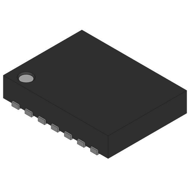


 工商网监
湘ICP备2023018690号
工商网监
湘ICP备2023018690号
