National Semiconductor is now part of
Texas Instruments.
Search http://www.ti.com/ for the latest technical
information and details on our current products and services.
�LMP7732
2.9 nV/sqrt(Hz) Low Noise, RRIO Amplifier
General Description
Features
The LMP7732 is a dual low noise, rail-to-rail input and output,
low voltage amplifier. The LMP7732 is part of the LMP® amplifier family and is ideal for precision and low noise applications with low voltage requirements.
This operational amplifier offers low voltage noise of 2.9 nV/
√Hz with a 1/f corner of only 3 Hz. The LMP7732 has bipolar
junction input stages with a bias current of only 1.5 nA. This
low input bias current, complemented by the very low level of
voltage noise, makes the LMP7732 an excellent choice for
photometry applications.
The LMP7732 provides a wide GBW of 22 MHz while consuming only 4 mA of current. This high gain bandwidth along
with the high open loop gain of 130 dB enables accurate signal conditioning in applications with high closed loop gain
requirements.
The LMP7732 has a supply voltage range of 1.8V to 5.5V,
making it an ideal choice for battery operated portable applications.
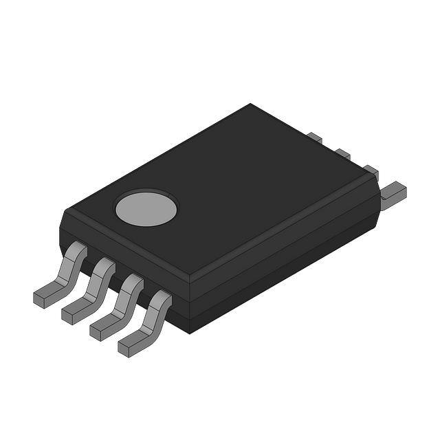
The LMP7732 is offered in the 8-Pin SOIC and MSOP packages.
The LMP7731 is the single version of this product and is offered in the 5-Pin SOT-23 and 8-Pin SOIC packages.
(Typical values, TA = 25°C, VS = 5V)
■ Input voltage noise
— f = 3 Hz
— f = 1 kHz
■ CMRR
■ Open loop gain
■ GBW
■ Slew rate
■ THD @ f = 10 kHz, AV = 1, RL = 2 kΩ
■ Supply current
■ Supply voltage range
■ Operating temperature range
■ Input bias current
■ RRIO
3.3 nV/√Hz
2.9 nV/√Hz
130 dB
130 dB
22 MHz
2.4 V/µs
0.001%
4.4 mA
1.8V to 5.5V
−40°C to 125°C
±1.5 nA
Applications
■ Gas analysis instruments
■ Photometric instrumentation
■ Medical instrumentation
Typical Performance Characteristics
Input Voltage Noise vs. Frequency
Input Current Noise vs. Frequency
30015063
30015064
LMP® is a registered trademark of National Semiconductor Corporation.
© 2011 Texas Instruments Incorporated
300150
www.ti.com
LMP7732 2.9 nV/sqrt(Hz) Low Noise, RRIO Amplifier
November 17, 2011
�LMP7732
Storage Temperature Range
Junction Temperature (Note 3)
Soldering Information
Infrared or Convection (20 sec)
Wave Soldering Lead Temp. (10 sec)
Absolute Maximum Ratings (Note 1)
If Military/Aerospace specified devices are required,
please contact the Texas Instruments Sales Office/
Distributors for availability and specifications.
ESD Tolerance (Note 2)
Human Body Model
For inputs pins only
For all other pins
Machine Model
Charge Device Model
VIN Differential
Supply Voltage (VS = V+ – V−)
Operating Ratings
2000V
2000V
200V
1000V
±2V
6.0V
2.5V Electrical Characteristics
−65°C to 150°C
+150°C max
235°C
260°C
(Note 1)
Temperature Range
Supply Voltage (VS = V+ – V–)
−40°C to 125°C
1.8V to 5.5V
Package Thermal Resistance (θJA)
8-Pin SOIC
8-Pin MSOP
190 °C/W
235°C/W
(Note 4)
Unless otherwise specified, all limits are guaranteed for TA = 25°C, V+ = 2.5V, V− = 0V, VCM = V+/2, RL >10 kΩ to V+/2. Boldface limits apply at the temperature extremes.
Symbol
VOS
TCVOS
IB
IOS
TCIOS
CMRR
Parameter
Input Offset Voltage
(Note 7)
Input Offset Voltage Temperature Drift
Conditions
VCM = 2.0V
±9
±500
±600
VCM = 0.5V
±9
±500
±600
VCM = 2.0V
±0.5
±5.5
VCM = 0.5V
±0.2
±5.5
VCM = 2.0V
±1
±30
±45
VCM = 0.5V
±12
±50
±75
VCM = 2.0V
±1
±50
±75
VCM = 0.5V
±11
±60
±80
Input Bias Current
Input Offset Current
Input Offset Current Drift
Common Mode Rejection Ratio
VCM = 0.5V and VCM = 2.0V
0.0474
0.15V ≤ VCM ≤ 0.7V
101
89
120
1.5V ≤ VCM ≤ 2.35V
105
99
129
2.5V ≤ V+ ≤ 5V
105
101
113
0.23V ≤ VCM ≤ 0.7V
1.5V ≤ VCM ≤ 2.27V
PSRR
Min
Typ
Max
(Note 6) (Note 5) (Note 6)
Power Supply Rejection Ratio
1.8V ≤ V+ ≤ 5.5V
CMVR
Common Mode Voltage Range
Large Signal CMRR ≥ 80 dB
AVOL
www.ti.com
Open Loop Voltage Gain
μV/°C
nA
nA
nA/°C
dB
dB
0
2.5
RL = 10 kΩ to
VOUT = 0.5V to 2.0V
130
RL = 2 kΩ to V+/2
VOUT = 0.5V to 2.0V
109
90
119
2
μV
111
112
104
V+/2
Units
V
dB
�Parameter
Conditions
Min
Typ
Max
(Note 6) (Note 5) (Note 6)
RL = 10 kΩ to V+/2
4
50
75
RL = 2 kΩ to V+/2
13
50
75
RL = 10 kΩ to V+/2
6
50
75
RL = 2 kΩ to V+/2
9
50
75
Output Voltage Swing High
VOUT
Output Voltage Swing Low
IOUT
IS
Output Current
Sourcing, VOUT = V+/2
VIN (diff) = 100 mV
22
12
31
Sinking, VOUT = V+/2
VIN (diff) = −100 mV
15
10
44
mV from
either rail
mA
VCM = 2.0V
4.0
5.4
6.8
VCM = 0.5V
4.6
6.2
7.8
Supply Current
Units
mA
SR
Slew Rate
AV = +1, CL = 10 pF, RL = 10 kΩ to V+/2
VOUT = 2 VPP
2.4
V/μs
GBW
Gain Bandwidth
CL = 20 pF, RL = 10 kΩ to V+/2
21
MHz
GM
Gain Margin
CL = 20 pF, RL = 10 kΩ to V+/2
14
dB
ΦM
Phase Margin
CL = 20 pF, RL = 10 kΩ to V+/2
60
deg
RIN
Input Resistance
THD+N
Total Harmonic Distortion + Noise
Input Referred Voltage Noise Density
en
Input Voltage Noise
in
Input Referred Current Noise Density
Differential Mode
38
kΩ
Common Mode
151
MΩ
0.002
%
AV = 1, fO = 1 kHz, Amplitude = 1V
f = 1 kHz, VCM = 2.0V
3.0
f = 1 kHz, VCM = 0.5V
3.0
0.1 Hz to 10 Hz
75
f = 1 kHz, VCM = 2.0V
1.1
f = 1 kHz, VCM = 0.5V
2.3
3.3V Electrical Characteristics
nV/
nVPP
pA/
(Note 4)
Unless otherwise specified, all limits are guaranteed for TA = 25°C, V+ = 3.3V, V− = 0V, VCM = V+/2, RL > 10 kΩ to V+/2. Boldface limits apply at the temperature extremes.
Symbol
VOS
TCVOS
IB
IOS
Parameter
Input Offset Voltage
(Note 7)
Input Offset Voltage Temperature Drift
Conditions
Min
Typ
Max
(Note 6) (Note 5) (Note 6)
VCM = 2.5V
±6
±500
±600
VCM = 0.5V
±6
±500
±600
VCM = 2.5V
±0.5
±5.5
VCM = 0.5V
±0.2
±5.5
VCM = 2.5V
±1.5
±30
±45
VCM = 0.5V
±13
±50
±77
VCM = 2.5V
±1
±50
±70
±11
±60
±80
Input Bias Current
Input Offset Current
VCM = 0.5V
3
Units
μV
μV/°C
nA
nA
www.ti.com
LMP7732
Symbol
�LMP7732
Symbol
TCIOS
CMRR
Parameter
Input Offset Current Drift
Common Mode Rejection Ratio
Conditions
Units
0.048
nA/°C
VCM = 0.5V and VCM = 2.5V
0.15V ≤ VCM ≤ 0.7V
101
89
120
1.5V ≤ VCM ≤ 3.15V
105
99
130
2.5V ≤ V+ ≤ 5.0V
105
101
113
0.23V ≤ VCM ≤ 0.7V
1.5V ≤ VCM ≤ 3.07V
PSRR
Min
Typ
Max
(Note 6) (Note 5) (Note 6)
Power Supply Rejection Ratio
1.8V ≤ V+ ≤ 5.5V
CMVR
Common Mode Voltage Range
Open Loop Voltage Gain
dB
111
Large Signal CMRR ≥ 80 dB
0
3.3
RL = 10 kΩ to
VOUT = 0.5V to 2.8V
112
104
130
RL = 2 kΩ to V+/2
VOUT = 0.5V to 2.8V
110
92
119
V+/2
AVOL
5
50
75
RL = 2 kΩ to V+/2
14
50
75
RL = 10 kΩ to V+/2
9
50
75
RL = 2 kΩ to V+/2
13
50
75
VOUT
Output Voltage Swing Low
IS
Output Current
Sourcing, VOUT = V+/2
VIN (diff) = 100 mV
28
22
45
Sinking, VOUT = V+/2
VIN (diff) = −100 mV
25
20
48
mV from
either rail
mA
VCM = 2.5V
4.2
5.6
7.0
VCM = 0.5V
4.8
6.4
8.0
Supply Current
V
dB
RL = 10 kΩ to V+/2
Output Voltage Swing High
IOUT
dB
mA
SR
Slew Rate
AV = +1, CL = 10 pF, RL = 10 kΩ to V+/2
VOUT = 2 VPP
2.4
V/μs
GBW
Gain Bandwidth
CL = 20 pF, RL = 10 kΩ to V+/2
22
MHz
GM
Gain Margin
CL = 20 pF, RL = 10 kΩ to V+/2
14
dB
ΦM
Phase Margin
CL = 20 pF, RL = 10 kΩ to
THD+N
Total Harmonic Distortion + Noise
AV = 1, fO = 1 kHz, Amplitude = 1V
RIN
Input Resistance
en
Input Referred Voltage Noise Density
Input Voltage Noise
in
www.ti.com
Input Referred Current Noise Density
62
deg
0.002
%
Differential Mode
38
kΩ
Common Mode
151
MΩ
f = 1 kHz, VCM = 2.5V
2.9
f = 1 kHz, VCM = 0.5V
2.9
V+/2
0.1 Hz to 10 Hz
75
f = 1 kHz, VCM = 2.5V
1.1
f = 1 kHz, VCM = 0.5V
2.1
4
nV/
nVPP
pA/
�(Note 4)
Unless otherwise specified, all limits are guaranteed for TA = 25°C, V+ = 5V, V− = 0V, VCM = V+/2, RL > 10 kΩ to V+/2. Boldface
limits apply at the temperature extremes.
Symbol
VOS
TCVOS
IB
IOS
TCIOS
CMRR
Parameter
Input Offset Voltage
(Note 7)
Input Offset Voltage Temperature Drift
Conditions
VCM = 4.5V
±6
±500
±600
VCM = 0.5V
±6
±500
±600
VCM = 4.5V
±0.5
±5.5
VCM = 0.5V
±0.2
±5.5
VCM = 4.5V
±1.5
±30
±50
VCM = 0.5V
±14
±50
±85
VCM = 4.5V
±1
±50
±70
VCM = 0.5V
±11
±65
±80
Input Bias Current
Input Offset Current
Input Offset Current Drift
Common Mode Rejection Ratio
VCM = 0.5V and VCM = 4.5V
0.0482
0.15V ≤ VCM ≤ 0.7V
101
89
120
1.5V ≤ VCM ≤ 4.85V
105
99
130
2.5V ≤ V+ ≤ 5V
105
101
113
0.23V ≤ VCM ≤ 0.7V
1.5V ≤ VCM ≤ 4.77V
PSRR
Min
Typ
Max
(Note 6) (Note 5) (Note 6)
Power Supply Rejection Ratio
1.8V ≤ V+ ≤ 5.5V
CMVR
Common Mode Voltage Range
Large Signal CMRR ≥ 80 dB
AVOL
Open Loop Voltage Gain
0
112
104
130
RL = 2 kΩ to V+/2
VOUT = 0.5V to 4.5V
110
94
119
50
75
RL = 2 kΩ to V+/2
24
50
75
RL = 10 kΩ to V+/2
9
50
75
RL = 2 kΩ to V+/2
23
50
75
Sourcing, VOUT = V+/2
VIN (diff) = 100 mV
33
27
47
Sinking, VOUT = V+/2
VIN (diff) = −100 mV
30
25
49
mV from
either rail
mA
4.4
6.0
7.4
VCM = 0.5V
5.0
6.8
8.4
Supply Current
V
dB
8
Output Voltage Swing Low
IS
nA
dB
RL = 10 kΩ to V+/2
VCM = 4.5V
nA
nA/°C
5
VOUT
Output Current
μV/°C
dB
Output Voltage Swing High
IOUT
μV
111
RL = 10 kΩ to
VOUT = 0.5V to 4.5V
V+/2
Units
mA
SR
Slew Rate
AV = +1, CL = 10 pF, RL = 10 kΩ to V+/2
VOUT = 2 VPP
2.4
V/μs
GBW
Gain Bandwidth
CL = 20 pF, RL = 10 kΩ to V+/2
22
MHz
5
www.ti.com
LMP7732
5V Electrical Characteristics
�LMP7732
Symbol
Parameter
Min
Typ
Max
(Note 6) (Note 5) (Note 6)
Conditions
Units
GM
Gain Margin
CL = 20 pF, RL = 10 kΩ to V+/2
12
dB
ΦM
Phase Margin
CL = 20 pF, RL = 10 kΩ to V+/2
65
deg
RIN
Input Resistance
Differential Mode
38
kΩ
151
MΩ
0.001
%
THD+ N Total Harmonic Distortion + Noise
Input Referred Voltage Noise Density
en
Input Voltage Noise
in
Input Referred Current Noise Density
Common Mode
AV = 1, fO = 1 kHz, Amplitude = 1V
f = 1 kHz, VCM = 4.5V
2.9
f = 1 kHz, VCM = 0.5V
2.9
0.1 Hz to 10 Hz
75
f = 1 kHz, VCM = 4.5V
1.1
f = 1 kHz, VCM = 0.5V
2.2
nV/
nVPP
pA/
Note 1: Absolute Maximum Ratings indicate limits beyond which damage to the device may occur. Operating Ratings indicate conditions for which the device is
intended to be functional, but specific performance is not guaranteed. For guaranteed specifications and the test conditions, see the Electrical Characteristics
Tables.
Note 2: Human Body Model, applicable std. MIL-STD-883, Method 3015.7. Machine Model, applicable std. JESD22-A115-A (ESD MM std. of JEDEC) FieldInduced Charge-Device Model, applicable std. JESD22-C101-C (ESD FICDM std. of JEDEC).
Note 3: The maximum power dissipation is a function of TJ(MAX), θJA, and TA. The maximum allowable power dissipation at any ambient temperature is
PD = (TJ(MAX) - TA)/ θJA. All numbers apply for packages soldered directly onto a PC board.
Note 4: Electrical Table values apply only for factory testing conditions at the temperature indicated. Factory testing conditions result in very limited self-heating
of the device such that TJ = TA. No guarantee of parametric performance is indicated in the electrical tables under conditions of internal self-heating where TJ >
TA. Absolute maximum Ratings indicate junction temperature limits beyond which the device maybe permanently degraded, either mechanically or electrically.
Note 5: Typical values represent the most likely parametric norm as determined at the time of characterization. Actual typical values may vary over time and will
also depend on the application and configuration. The typical values are not tested and are not guaranteed on shipped production material.
Note 6: All limits are guaranteed by testing, statistical analysis or design.
Note 7: Ambient production test is performed at 25°C with a variance of ±3°C.
Connection Diagram
8-Pin SOIC/MSOP
30015003
Top View
Ordering Information
Package
8-Pin SOIC
Part Number
LMP7732MA
LMP7732MAX
Package Marking
95 units/Rails
LMP7732MA
2.5k Units Tape and Reel
LMP7732MM
8-Pin MSOP
LMP7732MME
NSC Drawing
M08A
1k Units Tape and Reel
AZ3A
250 Units Tape and Reel
LMP7732MMX
www.ti.com
Transport Media
3.5k Units Tape and Reel
6
MUA08A
�Unless otherwise noted: TA = 25°C, RL > 10 kΩ, VCM = VS/2.
Offset Voltage Distribution
TCVOS Distribution
30015076
30015071
Offset Voltage Distribution
TCVOS Distribution
30015074
30015073
Offset Voltage Distribution
TCVOS Distribution
30015077
30015070
7
www.ti.com
LMP7732
Typical Performance Characteristics
�LMP7732
Offset Voltage Distribution
TCVOS Distribution
30015075
30015072
Offset Voltage vs. Temperature
Offset Voltage vs. Temperature
30015082
30015083
PSRR vs. Frequency
CMRR vs. Frequency
30015062
30015029
www.ti.com
8
�LMP7732
Offset Voltage vs. Supply Voltage
Offset Voltage vs. VCM
30015053
30015054
Offset Voltage vs. VCM
Offset Voltage vs. VCM
30015056
30015055
Input Offset Voltage Time Drift
Slew Rate vs. Supply Voltage
30015080
30015020
9
www.ti.com
�LMP7732
Time Domain Voltage Noise
Time Domain Voltage Noise
30015065
30015067
Time Domain Voltage Noise
Output Voltage vs. Output Current
30015066
30015057
Input Bias Current vs. VCM
Input Bias Current vs. VCM
30015026
30015025
www.ti.com
10
�Open Loop Frequency Response Over Temperature
30015018
30015027
Open Loop Frequency Response
Open Loop Frequency Response
30015028
30015019
THD+N vs. Frequency
THD+N vs. Output Voltage
30015085
30015069
11
www.ti.com
LMP7732
Input Bias Current vs. VCM
�LMP7732
Large Signal Step Response
Small Signal Step Response
30015022
30015021
Large Signal Step Response
Small Signal Step Response
30015024
30015023
Supply Current vs. Supply Voltage
Output Swing High vs. Supply Voltage
30015081
www.ti.com
30015058
12
�LMP7732
Output Swing Low vs. Supply Voltage
Sinking Current vs, Supply Voltage
30015059
30015060
Sourcing Current vs. Supply Voltage
30015061
13
www.ti.com
�LMP7732
Figure 1 shows that as the common mode voltage gets closer
to one of the extreme ends, current I1 significantly increases.
This increased current shows as an increase in voltage drop
across resistor R1 equal to I1*R1 on IN+ of the amplifier. This
voltage contributes to the offset voltage of the amplifier. When
common mode voltage is in the mid-range, the transistors are
operating in the linear region and I1 is significantly small. The
voltage drop due to I1 across R1 can be ignored as it is orders
of magnitude smaller than the amplifier's input offset voltage.
As the common mode voltage gets closer to one of the rails,
the offset voltage generated due to I1 increases and becomes
comparable to the amplifiers offset voltage.
Application Notes
LMP7732
The LMP7732 is a dual low noise, rail-to-rail input and output,
low voltage amplifier.
with a 1/f corThe low input voltage noise of only 2.9 nV/
ner at 3 Hz makes the LMP7732 ideal for sensor applications
where DC accuracy is of importance.
The LMP7732 has high gain bandwidth of 22 MHz. This wide
bandwidth enables the use of the amplifier at higher gain settings while retaining ample usable bandwidth for the application. This is particularly beneficial when system designers
need to use sensors with very limited output voltage range as
it allows larger gains in one stage which in turn increases signal to noise ratio.
The LMP7732 has a proprietary input bias cancellation circuitry on the input stages. This allows the LMP7732 to have
only about 1.5 nA bias current with a bipolar input stage. This
low input bias current, paired with the inherent lower input
voltage noise of bipolar input stages makes the LMP7732 an
excellent choice for precision applications. The combination
of low input bias current, low input offset voltage, and low input
voltage noise enables the user to achieve unprecedented accuracy and higher signal integrity.
National Semiconductor is heavily committed to precision
amplifiers and the market segment they serve. Technical support and extensive characterization data is available for sensitive applications or applications with a constrained error
budget.
The LMP7732 comes in the 8-Pin SOIC and MSOP packages. These small packages are ideal solutions for area
constrained PC boards and portable electronics.
30015006
FIGURE 1. Input Bias Current Cancellation
INPUT BIAS CURRENT CANCELLATION
The LMP7732 has proprietary input bias current cancellation
circuitry on its input stage.
The LMP7732 has rail-to-rail input. This is achieved by having
a p-input and n-input stage in parallel. Figure 1 only shows
one of the input stages as the circuitry is symmetrical for both
stages.
INPUT VOLTAGE NOISE MEASUREMENT
The LMP7732 has very low input voltage noise. The peak-topeak input voltage noise of the LMP7732 can be measured
using the test circuit shown in Figure 2
30015079
FIGURE 2. 0.1 Hz to 10 Hz Noise Test Circuit
The frequency response of this noise test circuit at the 0.1 Hz
corner is defined by only one zero. The test time for the
0.1 Hz to 10 Hz noise measurement using this configuration
should not exceed 10 seconds, as this time limit acts as an
www.ti.com
additional zero to reduce or eliminate the contributions of
noise from frequencies below 0.1 Hz.
Figure 3 shows typical peak-to-peak noise for the LMP7732
measured with the circuit in Figure 2.
14
�DIODES BETWEEN THE INPUTS
The LMP7732 has a set of anti-parallel diodes between their
input pins, as shown in Figure 5. These diodes are present to
protect the input stage of the amplifiers. At the same time,
they limit the amount of differential input voltage that is allowed on the input pins. A differential signal larger than the
voltage needed to turn on the diodes might cause damage to
the diodes. The differential voltage between the input pins
should be limited to ±3 diode drops or the input current needs
to be limited to ±20 mA.
30015066
FIGURE 3. 0.1 Hz to 10 Hz Input Voltage Noise
Measuring the very low peak-to-peak noise performance of
the LMP7732, requires special testing attention. In order to
achieve accurate results, the device should be warmed up for
at least five minutes. This is so that the input offset voltage of
the op amp settles to a value. During this warm up period, the
offset can typically change by a few µV because the chip
temperature increases by about 30°C. If the 10 seconds of
the measurement is selected to include this warm up time,
some of this temperature change might show up as the measured noise.Figure 4 shows the start-up drift of five typical
LMP7732 units.
30015004
FIGURE 5. Anti-Parallel Diodes between Inputs
30015080
FIGURE 4. Start-Up Input Offset Voltage Drift
15
www.ti.com
LMP7732
During the peak-to-peak noise measurement, the LMP7732
must be shielded. This prevents offset variations due to airflow. Offset can vary by a few nV due to this airflow and that
can invalidate measurements of input voltage noise with a
magnitude which is in the same range. For similar reasons,
sudden motions must also be restricted in the vicinity of the
test area. The feed-through which results from this motion
could increase the observed noise value which in turn would
invalidate the measurement.
�LMP7732
DRIVING AN ADC
Analog to Digital Converters, ADCs, usually have a sampling
capacitor on their input. When the ADC's input is directly connected to the output of the amplifier a charging current flows
from the amplifier to the ADC. This charging current causes
a momentary glitch that can take some time to settle. There
are different ways to minimize this effect. One way is to slow
down the sampling rate. This method gives the amplifier sufficient time to stabilize its output. Another way to minimize the
glitch, caused by the switch capacitor, is to have an external
capacitor connected to the input of the ADC. This capacitor is
chosen so that its value is much larger than the internal
switching capacitor and it will hence provide the charge needed to quickly and smoothly charge the ADC's sampling capacitor. Since this large capacitor will be loading the output of
the amplifier as well, an isolation resistor is needed between
the output of the amplifier and this capacitor. The isolation
resistor, RISO, separates the additional load capacitance from
the output of the amplifier and will also form a low-pass filter
and can be designed to provide noise reduction as well as
anti-aliasing. The draw back of having RISO is that it reduces
signal swing since there is some voltage drop across it.
Figure 6 (a) shows the ADC directly connected to the amplifier. To minimize the glitch in this setting, a slower sample rate
needs to be used. Figure 6 (b) shows RISO and an external
capacitor used to minimize the glitch.
30015005
FIGURE 6. Driving An ADC
www.ti.com
16
�LMP7732
Physical Dimensions inches (millimeters) unless otherwise noted
8-Pin SOIC
NS Package Number M08A
8-Pin MSOP
NS Package Number MUA08A
17
www.ti.com
�LMP7732 2.9 nV/sqrt(Hz) Low Noise, RRIO Amplifier
Notes
TI/NATIONAL INTERIM IMPORTANT NOTICE
Texas Instruments has purchased National Semiconductor. As of Monday, September 26th, and until further notice, products sold or
advertised under the National Semiconductor name or logo, and information, support and interactions concerning such products, remain
subject to the preexisting National Semiconductor standard terms and conditions of sale, terms of use of website, and Notices (and/or
terms previously agreed in writing with National Semiconductor, where applicable) and are not subject to any differing terms and notices
applicable to other TI components, sales or websites. To the extent information on official TI and National websites and business social
networking media, etc., pertains to both TI and National-branded products, both companies' instructions, warnings and limitations in the
above-referenced terms of use apply.
Following are URLs where you can obtain information on other Texas Instruments products and application solutions:
Products
Applications
Audio
www.ti.com/audio
Communications and Telecom
www.ti.com/communications
Amplifiers
amplifier.ti.com
Computers and Peripherals
www.ti.com/computers
Data Converters
dataconverter.ti.com
Consumer Electronics
www.ti.com/consumer-apps
DLP® Products
www.dlp.com
Energy and Lighting
www.ti.com/energy
DSP
dsp.ti.com
Industrial
www.ti.com/industrial
Clocks and Timers
www.ti.com/clocks
Medical
www.ti.com/medical
Interface
interface.ti.com
Security
www.ti.com/security
Logic
logic.ti.com
Space, Avionics and Defense
www.ti.com/space-avionicsdefense
Power Mgmt
power.ti.com
Transportation and Automotive
www.ti.com/automotive
Microcontrollers
microcontroller.ti.com Video and Imaging
www.ti.com/video
RFID
www.ti-rfid.com
www.ti.com/wireless-apps
RF/IF and ZigBee® Solutions www.ti.com/lprf
Wireless
TI E2E Community Home Page e2e.ti.com
Mailing Address: Texas Instruments, Post Office Box 655303, Dallas, Texas 75265
Copyright© 2011 Texas Instruments Incorporated
www.ti.com
�


 工商网监
湘ICP备2023018690号
工商网监
湘ICP备2023018690号
