Order
Now
Product
Folder
Support &
Community
Tools &
Software
Technical
Documents
LMR36506-Q1
SNVSB91C – JULY 2019 – REVISED JUNE 2020
LMR36506-Q1 3-V to 65-V, 0.6-A Synchronous Buck Converter Optimized for Size and
Light Load Efficiency
1 Features
3 Description
•
The LMR36506-Q1 is the industry's smallest 65 V,
0.6 A synchronous step-down DC/DC converter in 2mm x 2-mm HotRod™ package. This easy-to-use
converter can handle input voltage transients up to 70
V, provide excellent EMI performance and support
fixed 3.3 V, 5 V and other adjustable output voltages.
1
•
•
•
•
AEC-Q100-qualified for automotive applications:
– Device temperature grade 1: –40°C to +125°C,
TA
Functional Safety-Capable
– Documentation available to aid functional
safety system design
>80% efficiency at 1 mA
– 4 µA Iq (switching) at 24 VIN to 3.3 VOUT (fixed
output option)
Miniature solution size and low component cost
– 2-mm × 2-mm HotRod™ package with
wettable flanks
– Internal compensation
Designed for automotive applications:
– Junction temperature range –40°C to +150°C
– Pseudo-random spread spectrum compatible
with CISPR 25 EMI standard
– Wide input voltage range: 3.0 V (falling
threshold) to 65 V
– Adjustable, 3.3-V and 5-V fixed output voltage
options available
– Synchronizable with MODE/SYNC pin variant
– Adjustable FSW: 200 kHz to 2.2 MHz with RT
pin variant
– Pin compatible with LMR36503-Q1 (65 V, 300
mA)
The LMR36506-Q1 uses peak current mode control
architecture with internal compensation and maintains
stable operation with minimal output capacitance. The
wide input operating range of the LMR36506-Q1
helps it remain functional during a deep input voltage
sag condition, making it an excellent choice for
automotive applications withstanding severe cold
crank start impulses. The PGOOD flag in the
LMR36506-Q1 provides precise indication of the
output voltage status, eliminating the requirement for
an external supervisor. A seamless transition from
FPWM to PFM, with an ultra-low standby quiescent
current allows the LMR36506-Q1 to support much
higher system efficiency at low output loads. The
MODE/SYNC pin variant helps to synchronize the
LMR36506-Q1 to an external clock. With the right
resistor selection, the LMR36506-Q1 RT pin variant
can also be externally programmed to any desired
switching frequency of operation. The rich feature set
of the LMR36506-Q1 is designed to simplify
implementation for a wide range of automotive end
equipments.
Device Information(1)
PART NUMBER
LMR36506-Q1
2 Applications
•
•
•
Advanced driver assistance systems (ADAS)
Body electronics and lighting
Infotainment and cluster
Efficiency versus Output Current
VOUT = 3.3 V (Fixed), 2.2 MHz
BOOT
VIN
CIN
100
CBOOT
90
EN/
UVLO
SW
VOUT
LIND
80
COUT
PGOOD
RFBT
CVCC
FB
GND
RFBB
70
Efficiency (%)
MODE/
SYNC
VCC
BODY SIZE (NOM)
2.00 mm × 2.00 mm
(1) For all available packages, see the orderable addendum at
the end of the data sheet.
Simplified Schematic
VIN
PACKAGE
VQFN-HR (9)
60
50
40
30
VIN = 8V
VIN = 13.5V
VIN = 24V
VIN = 48V
20
10
0
10P
100P
1m
10m
Load Current (A)
100m
1
LMR3
1
An IMPORTANT NOTICE at the end of this data sheet addresses availability, warranty, changes, use in safety-critical applications,
intellectual property matters and other important disclaimers. PRODUCTION DATA.
�LMR36506-Q1
SNVSB91C – JULY 2019 – REVISED JUNE 2020
www.ti.com
Table of Contents
1
2
3
4
5
6
7
Features ..................................................................
Applications ...........................................................
Description .............................................................
Revision History.....................................................
Device Comparison Table.....................................
Pin Configuration and Functions .........................
Specifications.........................................................
7.1
7.2
7.3
7.4
7.5
7.6
7.7
7.8
7.9
8
1
1
1
2
3
4
5
Absolute Maximum Ratings ...................................... 5
ESD (Automotive) Ratings ........................................ 5
Recommended Operating Conditions....................... 5
Thermal Information .................................................. 5
Electrical Characteristics........................................... 6
Timing Characteristics............................................... 8
Switching Characteristics .......................................... 8
System Characteristics ............................................. 8
Typical Characteristics ............................................ 10
Detailed Description ............................................ 11
8.1 Overview ................................................................. 11
8.2 Functional Block Diagram ....................................... 12
8.3 Feature Description................................................. 13
8.4 Device Functional Modes........................................ 24
9
Application and Implementation ........................ 30
9.1 Application Information............................................ 30
9.2 Typical Application .................................................. 31
9.3 What to Do and What Not to Do ............................. 42
10 Power Supply Recommendations ..................... 42
11 Layout................................................................... 43
11.1 Layout Guidelines ................................................. 43
11.2 Layout Example .................................................... 45
12 Device and Documentation Support ................. 46
12.1
12.2
12.3
12.4
12.5
12.6
Documentation Support ........................................
Receiving Notification of Documentation Updates
Support Resources ...............................................
Trademarks ...........................................................
Electrostatic Discharge Caution ............................
Glossary ................................................................
46
46
46
46
46
46
13 Mechanical, Packaging, and Orderable
Information ........................................................... 46
4 Revision History
NOTE: Page numbers for previous revisions may differ from page numbers in the current version.
Changes from Revision B (February 2020) to Revision C
•
2
Page
Changed device status from Advance Information to Production Data ................................................................................. 1
Submit Documentation Feedback
Copyright © 2019–2020, Texas Instruments Incorporated
Product Folder Links: LMR36506-Q1
�LMR36506-Q1
www.ti.com
SNVSB91C – JULY 2019 – REVISED JUNE 2020
5 Device Comparison Table
ORDERABLE PART NUMBER
OUTPUT VOLTAGE
EXTERNAL SYNC
FSW
SPREAD SPECTRUM
LMR36506MSCQRPERQ1
Adjustable
Yes
(PFM/FPWM
Selectable)
Fixed
2.2 MHz
Yes
LMR36506MSC5RPERQ1
5-V Fixed
Yes
(PFM/FPWM
Selectable)
Fixed
2.2 MHz
Yes
LMR36506MSC3RPERQ1
3.3-V Fixed
Yes
(PFM/FPWM
Selectable)
Fixed
2.2 MHz
Yes
LMR36506RS3QRPERQ1
3.3-V Fixed
No
(Default PFM at light
load)
Adjustable
with RT resistor
Yes
Submit Documentation Feedback
Copyright © 2019–2020, Texas Instruments Incorporated
Product Folder Links: LMR36506-Q1
3
�LMR36506-Q1
SNVSB91C – JULY 2019 – REVISED JUNE 2020
www.ti.com
6 Pin Configuration and Functions
RPE Package
9-Pin (2 mm x 2 mm) VQFN-HR
Top View
GND
RT(1)
MODE/SYNC(2)
1
9
FB(4)
8
VOUT/BIAS(3)
PGOOD
2
7
VCC
EN/UVLO
3
6
BOOT
VIN
4
5
SW
(1)
See Device Comparison Table for more details. Pin 1 trimmed and factory-set for externally adjustable switching
frequency RT variants only.
(2)
Pin 1 factory-set for fixed switching frequency MODE/SYNC variants only.
(3)
Pin 8 trimmed and factory-set for fixed output voltage VOUT/BIAS variants only.
(4)
Pin 8 factory-set for adjustable output voltage FB variants only.
Pin Functions
PIN
NO.
NAME
I/O
DESCRIPTION
1
RT
or MODE/SYNC
A
When part is trimmed as the RT variant, the switching frequency can be adjusted from 200 kHz to
2.2 MHz.
When the part is trimmed as the MODE/SYNC variant, it can operate in user-selectable
PFM/FPWM mode and can be synchronized to an external clock.
Do not float this pin.
2
PGOOD
A
Open-drain power-good flag output. Connect to suitable voltage supply through a current limiting
resistor. High = power OK, low = power bad. It goes low when EN = low. It can be open or
grounded when not used.
3
EN/UVLO
A
Enable input to regulator. High = ON, low = OFF. Can be connected directly to VIN. Do not float
this pin.
4
VIN
P
Input supply to regulator. Connect a high-quality bypass capacitor or capacitors directly to this pin
and GND.
5
SW
P
Regulator switch node. Connect to power inductor.
6
BOOT
P
Bootstrap supply voltage for internal high-side driver. Connect a high-quality 100-nF capacitor from
this pin to the SW pin.
7
VCC
P
Internal LDO output. Used as supply to internal control circuits. Do not connect to external loads.
Can be used as logic supply for power-good flag. Connect a high-quality 1-µF capacitor from this
pin to GND.
8
VOUT/BIAS or FB
A
Fixed output options are available with the VOUT/BIAS pin variant. Connect to output voltage node
for fixed VOUT. Check the Device Comparison Table for more details.
The FB pin variant can help adjust the output voltage. Connect to tap point of feedback voltage
divider. Do not float this pin.
9
GND
G
Power ground terminal. Connect to system ground. Connect to CIN with short, wide traces.
A = Analog, P = Power, G = Ground
4
Submit Documentation Feedback
Copyright © 2019–2020, Texas Instruments Incorporated
Product Folder Links: LMR36506-Q1
�LMR36506-Q1
www.ti.com
SNVSB91C – JULY 2019 – REVISED JUNE 2020
7 Specifications
7.1 Absolute Maximum Ratings
Over the recommended operating junction temperature range (1)
MIN
MAX
VIN to GND
PARAMETER
–0.3
70
V
EN to GND
–0.3
70
V
SW to GND
–0.3
70.3
V
0
20
V
VOUT/BIAS to GND (Fixed output)
–0.3
16
V
FB to GND - (Adjustable output)
–0.3
16
V
BOOT to SW
–0.3
5.5
V
VCC to GND
–0.3
5.5
V
RT to GND (RT variant)
–0.3
5.5
V
MODE/SYNC to GND (MODE/SYNC variant)
–0.3
5.5
V
TJ
Junction temperature
–40
150
°C
Tstg
Storage temperature
–65
150
°C
PGOOD to GND
Voltage
(1)
UNIT
Stresses beyond those listed under Absolute Maximum Ratings may cause permanent damage to the device. These are stress ratings
only, which do not imply functional operation of the device at these or any other conditions beyond those indicated under
Recommended Operating Conditions. Exposure to absolute-maximum-rated conditions for extended periods may affect device
reliability.
7.2 ESD (Automotive) Ratings
V(ESD)
(1)
Electrostatic discharge
VALUE
UNIT
Human-body model (HBM), per AEC Q100002 (1) HBM ESD classification level 2
±2000
V
Charged-device model (CDM), per AEC Q100011 CDM ESD classification level C5
±750
V
AEC Q100-002 indicates that HBM stressing shall be in accordance with the ANSI/ESDA/JEDEC JS-001 specification.
7.3 Recommended Operating Conditions
Over the recommended operating junction temperature range of –40 °C to 150 °C (unless otherwise noted) (1) (2)
MIN
Input
voltage
Input voltage range after startup
Output
current
Load current range (3)
Selectable frequency range with RT (RT variant only)
Frequency
Set frequency value with RT connected to GND (RT variant only)
setting
Set frequency value with RT connected to VCC (RT variant only)
External
clock
setting
(1)
(2)
(3)
External Sync CLK (MODE/SYNC variant only)
TYP
MAX
UNIT
3.6
65
V
0
0.6
A
2.2
MHz
0.2
0.2
2.2
MHz
1
MHz
2.2
MHz
Recommended operating conditions indicate conditions for which the device is intended to be functional, but do not ensure specific
performance limits. For ensured specifications, see Electrical Characteristics table.
High junction temperatures degrade operating lifetimes. Operating lifetime is de-rated for junction temperatures greater than 125℃
Maximum continuous DC current may be derated when operating with high switching frequency and/or high ambient temperature. See
Application section for details.
7.4 Thermal Information
The value of RθJA given in this table is only valid for comparison with other packages and cannot be used for design purposes.
These values were calculated in accordance with JESD 51-7, and simulated on a 4-layer JEDEC board. They do not
represent the performance obtained in an actual application. For example, with a 4-layer PCB, a RθJA= 58℃/W can be
achieved
Submit Documentation Feedback
Copyright © 2019–2020, Texas Instruments Incorporated
Product Folder Links: LMR36506-Q1
5
�LMR36506-Q1
SNVSB91C – JULY 2019 – REVISED JUNE 2020
www.ti.com
Thermal Information (continued)
The value of RθJA given in this table is only valid for comparison with other packages and cannot be used for design purposes.
These values were calculated in accordance with JESD 51-7, and simulated on a 4-layer JEDEC board. They do not
represent the performance obtained in an actual application. For example, with a 4-layer PCB, a RθJA= 58℃/W can be
achieved
LMR36506-Q1
THERMAL METRIC (1)
VQFN (RPE)
UNIT
9 Pins
RθJA
Junction-to-ambient thermal resistance
84.4
°C/W
RθJC(top)
Junction-to-case (top) thermal resistance
47.5
°C/W
RθJB
Junction-to-board thermal resistance
26.1
°C/W
ΨJT
Junction-to-top characterization parameter
0.9
°C/W
ΨJB
Junction-to-board characterization parameter
25.9
°C/W
(1)
For more information about traditional and new thermal metrics, see the Semiconductor and IC Package Thermal Metrics application
report. The value of RΘJA given in this table is only valid for comparison with other packages and can not be used for design purposes.
This value was calculated in accordance with JESD 51-7, and simulated on a 4-layer JEDEC board. It does not represent the
performance obtained in an actual application. For design information see the Maximum Ambient Temperature section.
7.5 Electrical Characteristics
Limits apply over the recommended operating junction temperature (TJ) range of –40°C to +150°C, unless otherwise stated.
Minimum and maximum limits are specified through test, design or statistical correlation. Typical values represent the most
likely parametric norm at TJ = 25°C, and are provided for reference purposes only. Unless otherwise stated, the following
conditions apply: VIN = 24 V. (1)
PARAMETER
TEST CONDITIONS
MIN
TYP
MAX
3.4
3.5
UNIT
SUPPLY VOLTAGE (VIN PIN)
VIN_R
Minimum operating input voltage
(rising)
Rising threshold
VIN_F
Minimum operating input voltage
(falling)
Once operating; Falling threshold
2.45
3.0
IQ_13p5_Fixed
Non-switching input current;
measured at VIN pin (2)
VIN = VEN = 13.5V ; VOUT/BIAS = 5.25V,
VMODE/SYNC = VRT = 0V; Fixed output
0.25
0.672
1.05
µA
IQ_13p5_Adj
Non-switching input current;
measured at VIN pin (2)
VIN = VEN = 13.5V ; VFB = 1.05V,
VMODE/SYNC = VRT = 0V; Adjustable
output
14
17
22
µA
IQ_24p0_Fixed
Non-switching input current;
measured at VIN pin(2)
VIN = VEN = 24V ; VOUT/BIAS =
5.25V, VMODE/SYNC = VRT = 0V; Fixed
output
0.8
1.2
1.7
µA
IQ_24p0_Adj
Non-switching input current;
measured at VIN pin (2)
VIN = VEN = 24V ; VFB = 1.05V,
VMODE/SYNC = VRT = 0V; Adjustable
output
14
18
22
µA
IB_13p5
Current into VOUT/BIAS pin (not
switching) (2)
VIN = 13.5V, VOUT/BIAS = 5.25V,
VMODE/SYNC = VRT = 0V; Fixed output
14
17
22
µA
IB_24p0
Current into VOUT/BIAS pin (not
switching) (2)
VIN = 24V, VOUT/BIAS = 5.25V,
VMODE/SYNC = VRT = 0V; Fixed output
14
18
22
µA
ISD_13p5
Shutdown quiescent current;
measured at VIN pin (2)
VEN = 0; VIN = 13.5V
0.5
1.1
µA
ISD_24p0
Shutdown quiescent current;
measured at VIN pin (2)
VEN = 0; VIN = 24V
1
1.6
µA
V
V
ENABLE (EN PIN)
VEN-WAKE
Enable wake-up threshold
VEN-VOUT
Precision enable high level for
VOUT
(1)
(2)
6
0.4
1.16
V
1.263
1.36
V
MIN and MAX limits are 100% production tested at 25ºC. Limits over the operating temperature range verified through correlation using
Statistical Quality Control (SQC) methods. Limits are used to calculate Average Outgoing Quality Level (AOQL).
This is the current used by the device open loop. It does not represent the total input current of the system when in regulation.
Submit Documentation Feedback
Copyright © 2019–2020, Texas Instruments Incorporated
Product Folder Links: LMR36506-Q1
�LMR36506-Q1
www.ti.com
SNVSB91C – JULY 2019 – REVISED JUNE 2020
Electrical Characteristics (continued)
Limits apply over the recommended operating junction temperature (TJ) range of –40°C to +150°C, unless otherwise stated.
Minimum and maximum limits are specified through test, design or statistical correlation. Typical values represent the most
likely parametric norm at TJ = 25°C, and are provided for reference purposes only. Unless otherwise stated, the following
conditions apply: VIN = 24 V.(1)
PARAMETER
TEST CONDITIONS
VEN-HYST
Enable threshold hysteresis below
VEN-VOUT
ILKG-EN
Enable input leakage current
VEN = 3.3 V
VCC
Internal VCC voltage
Adjustable or fixed output; Auto mode
ICC
Bias regulator current limit
VCC-UVLO
Internal VCC undervoltage lockout VCC rising under voltage threshold
VCC-UVLO-HYST
Internal VCC under voltage lockout hysteresis
MIN
TYP
MAX
UNIT
0.3
0.35
0.4
V
0.3
8
nA
3.15
3.22
V
65
240
mA
3
3.3
3.65
V
0.4
0.8
1.2
V
0.87
1
1.11
A
0.6
0.7
0.752
A
0.127
0.19
0.227
A
0
0.01
0.022
A
INTERNAL LDO
Hysteresis below VCC-UVLO
3.125
CURRENT LIMITS
ISC-0p6
Short circuit high side current
Limit (3)
ILS-LIMIT-0p6
Low side current limit (3)
(3)
IPEAK-MIN-0p6
Minimum Peak Inductor Current
IZC
Zero cross current (3)
Auto Mode, duty factor = 0
Auto mode
IL-NEG
Sink current limit (negative) (3)
FPWM mode
0.6
0.7
0.8
A
PG-OV
PGOOD upper threshold - rising
% of FB (Adjustable output) or % of
VOUT/BIAS (Fixed output)
106
107
110
%
PG-UV
PGOOD lower threshold - falling
% of FB (Adjustable output) or % of
VOUT/BIAS (Fixed output)
93
94
96.5
%
PG-HYS
PGOOD hysteresis - rising/falling
% of FB (Adjustable output) or % of
VOUT/BIAS (Fixed output)
1.3
1.8
2.3
%
VPG-VALID
Minimum input voltage for proper
PG function
0.75
1
2
V
RPG-EN5p0
RDS(ON) PGOOD output
VEN = 5.0V, 1mA pull-up current
20
40
70
Ω
RPG-EN0
RDS(ON) PGOOD output
VEN = 0 V, 1mA pull-up current
10
18
31
Ω
POWER GOOD
OSCILLATOR (MODE/SYNC)
VMODE_H
Sync input and mode high level
threshold
1.8
VSYNC-HYS
Sync input hysteresis
230
VMODE_L
Sync input and mode low level
threshold
V
300
380
mV
0.8
V
MOSFETS
RDS-ON-HS
High-side MOSFET on-resistance
Load = 0.3 A
560
920
mΩ
RDS-ON-LS
Low-side MOSFET on-resistance
Load = 0.3 A
280
460
mΩ
VCBOOT-UVLO
Cboot - SW UVLO threshold (4)
2.14
2.3
2.42
V
VOLTAGE REFERENCE
VOUT_Fixed3p3
Initial VOUT voltage accuracy for
3.3 V
FPWM mode
3.25
3.3
3.34
V
VOUT_Fixed5p0
Initial VOUT voltage accuracy for
5V
FPWM mode
4.93
5
5.07
V
VREF
Internal reference voltage
VIN = 3.6V to 65V, FPWM mode
1
1.01
V
IFB
FB input current
Adjustable output, FB = 1V
85
110
nA
(3)
(4)
0.985
The current limit values in this table are tested, open loop, in production. They may differ from those found in a closed loop application.
When the voltage across the CBOOT capacitor falls below this voltage, the low side MOSFET is turn to recharge the boot capacitor
Submit Documentation Feedback
Copyright © 2019–2020, Texas Instruments Incorporated
Product Folder Links: LMR36506-Q1
7
�LMR36506-Q1
SNVSB91C – JULY 2019 – REVISED JUNE 2020
www.ti.com
7.6 Timing Characteristics
Limits apply over the recommended operating junction temperature (TJ) range of –40°C to +150°C, unless otherwise stated.
Minimum and maximum limits are specified through test, design or statistical correlation. Typical values represent the most
likely parametric norm at TJ = 25°C, and are provided for reference purposes only. Unless otherwise stated, the following
conditions apply: VIN = 24 V. (1)
PARAMETER
TEST CONDITIONS
MIN
TYP
MAX
UNIT
1.95
2.58
3.2
ms
SOFT START
Time from first SW pulse to VFB at
90%, of VREF
tSS
VIN ≥ 3.6 V
POWER GOOD
tRESET_FILTER
Glitch filter time constant for PG
function
15
25
40
µs
tPGOOD_ACT
Delay time to PG high signal
1.7
1.956
2.16
ms
OSCILLATOR (MODE/SYNC)
tPULSE_H
High duration needed to be
recognized as a pulse
100
ns
tPULSE_L
Low duration needed to be
recognized as a pulse
100
ns
tSYNC
High/low signal duration in a valid
synchronization signal
tMODE
Time at one level needed to indicate
FPWM or Auto Mode
(1)
6
9
12
18
µs
µs
MIN and MAX limits are 100% production tested at 25°C. Limits over the operating temperature range are verified through correlation
usingStatistical Quality Control (SQC) methods. Limits are used to calculate Average Outgoing Quality Level (AOQL).
7.7 Switching Characteristics
Limits apply over the recommended operating junction temperature (TJ) range of –40°C to +150°C, unless otherwise stated.
Minimum and maximum limits are specified through test, design or statistical correlation. Typical values represent the most
likely parametric norm at TJ = 25°C, and are provided for reference purposes only. Unless otherwise stated, the following
conditions apply: VIN = 24 V. (1)
PARAMETER
TEST CONDITIONS
MIN
TYP
MAX
UNIT
40
57
80
40
58
77
ns
7.6
9
9.8
µs
PWM LIMITS (SW)
tON-MIN
Minimum switch on-time
tOFF-MIN
Minimum switch off-time
tON-MAX
Maximum switch on-time
VIN =24 V, IOUT = 0.6 A
HS timeout in dropout
ns
OSCILLATOR (RT)
fOSC_2p2MHz
Internal oscillator frequency
RT = GND
2.1
2.2
2.3
MHz
fOSC_1p0MHz
Internal oscillator frequency
RT = VCC
0.93
1
1.05
MHz
RT = 39.2 kΩ
0.34
0.4
0.46
MHz
fADJ_400kHz
(1)
MIN and MAX limits are 100% production tested at 25°C. Limits over the operating temperature range are verified through correlation
usingStatistical Quality Control (SQC) methods. Limits are used to calculate Average Outgoing Quality Level (AOQL).
7.8 System Characteristics
The following specifications apply only to the typical applications circuit, with nominal component values. Specifications in the
typical (TYP) column apply to TJ = 25°C only. Specifications in the minimum (MIN) and maximum (MAX) columns apply to the
case of typical components over the temperature range of TJ = –40°C to 150°C. These specifications are not ensured by
production testing.
PARAMETER
TEST CONDITIONS
MIN
TYP
MAX
UNIT
STANDBY CURRENT AND DUTY RATIO
ISUPPLY
8
Input supply current when in
regulation
VIN = 13.5 V, VOUT/BIAS = 3.3 V, IOUT
= 0 A, PFM mode
Submit Documentation Feedback
6.5
µA
Copyright © 2019–2020, Texas Instruments Incorporated
Product Folder Links: LMR36506-Q1
�LMR36506-Q1
www.ti.com
SNVSB91C – JULY 2019 – REVISED JUNE 2020
System Characteristics (continued)
The following specifications apply only to the typical applications circuit, with nominal component values. Specifications in the
typical (TYP) column apply to TJ = 25°C only. Specifications in the minimum (MIN) and maximum (MAX) columns apply to the
case of typical components over the temperature range of TJ = –40°C to 150°C. These specifications are not ensured by
production testing.
PARAMETER
ISUPPLY
Input supply current when in
regulation
DMAX
Maximum switch duty cycle (1)
TEST CONDITIONS
MIN
VIN = 24 V, VOUT/BIAS = 3.3 V, IOUT =
0 A, PFM mode
TYP
MAX
4
UNIT
µA
98%
OUTPUT VOLTAGE ACCURACY (VOUT/BIAS)
VOUT_3p3V_ACC
VOUT = 3.3 V, VIN = 3.6 V to 65 V,
IOUT = 0 to full load (2)
FPWM mode
–1.5
1.5
%
VOUT_3p3V_ACC
VOUT = 3.3 V, VIN = 3.6V to 65 V,
IOUT = 0 A to full load (2)
Auto mode
–1.5
2.5
%
SPREAD SPECTRUM
Frequency span of spread
spectrum operation - largest
deviation from center frequency
fSSS
Spread spectrum active
±2
Spread spectrum pseudo random
pattern frequency
fPSS
%
0.98
1.5
Hz
THERMAL SHUTDOWN
TSD-R
Thermal shutdown rising
Shutdown threshold
158
168
180
°C
TSD-F
Thermal shutdown falling
Recovery threshold
150
158
165
°C
TSD-HYS
Thermal shutdown hysteresis
8
10
15
°C
(1)
(2)
In dropout the switching frequency drops to increase the effective duty cycle. The lowest frequency is clamped at approximately: fMIN = 1
/ (tON-MAX + TOFF-MIN). DMAX = tON-MAX /(tON-MAX + tOFF-MIN).
Deviation is with respect to VIN =13.5 V
Submit Documentation Feedback
Copyright © 2019–2020, Texas Instruments Incorporated
Product Folder Links: LMR36506-Q1
9
�LMR36506-Q1
SNVSB91C – JULY 2019 – REVISED JUNE 2020
www.ti.com
7.9 Typical Characteristics
Unless otherwise specified, the following conditions apply: TA = 25°C, VIN = 13.5 V
90
80
80
70
70
Efficiency (%)
100
90
Efficiency (%)
100
60
50
40
30
10
0
1m
10m
100m
Load Current (A)
VOUT = 3.3 V Fixed
50
40
30
VIN = 8V
VIN = 13.5V
VIN = 24V
VIN = 48V
20
60
VIN = 8V
VIN = 13.5V
VIN = 24V
VIN = 48V
20
10
0
1m
1
10m
100m
Load Current (A)
LMR3
FSW = 2.2 MHz (FPWM)
VOUT = 5 V Fixed
Figure 1. Efficiency 3.3-V Output, FPWM
1
LMR3
FSW = 2.2 MHz (FPWM)
Figure 2. Efficiency 5-V Output, FPWM
100
18
90
3.3V
5V
16
Quiescent Current (PA)
80
Efficiency (%)
70
60
50
40
30
VIN = 8V
VIN = 13.5V
VIN = 24V
VIN = 48V
20
10
0
10P
100P
VOUT = 5 V Fixed
1m
10m
Load Current (A)
100m
Input Voltage (V)
6
5
5
4
4
3
3
2
2
1
Power-Down 1
Power-Up
0
6
7
0
VOUT = 5 V Fixed
5
10
15
20
25
30 35 40 45
Input Voltage (V)
50
55
60
65
Inpu
Figure 4. Typical Input Supply Current at
No Load for Fixed 3.3-V and 5-V Output
VOUT (1V/DIV)
VIN (1V/DIV)
IOUT (200mA/DIV)
50ms/DIV
D006
FSW-NOM = 2.2 MHz
(Auto)
Figure 5. Dropout at Power-Up and Power-Down
10
Output Voltage (V)
6
ILoad = 300 mA
6
5
FSW-NOM = 2.2 MHz (Auto)
3
4
Input Voltage (V)
8
LMR3
7
2
10
2
1
Figure 3. Efficiency 5-V Output, Auto Mode
1
12
4
7
0
14
Figure 6. Typical Start-up and Shutdown at
VOUT = 5 V
Submit Documentation Feedback
Copyright © 2019–2020, Texas Instruments Incorporated
Product Folder Links: LMR36506-Q1
�LMR36506-Q1
www.ti.com
SNVSB91C – JULY 2019 – REVISED JUNE 2020
8 Detailed Description
8.1 Overview
The LMR36506-Q1 is a wide input, low-quiescent current, high-performance regulator that can operate over a
wide range of duty ratio and the switching frequencies, including sub-AM band at 400 kHz and above AM band at
2.2 MHz. During wide input transients, if the minimum ON-time or the minimum OFF-time cannot support the
desired duty ratio at the higher switching frequency settings, the switching frequency is reduced automatically,
allowing the LMR36506-Q1 to maintain the output voltage regulation. With an internally-compensated design
optimized for minimal output capacitors, the system design process with the LMR36506-Q1 is simplified
significantly compared to other buck regulators available in the market.
The LMR36506-Q1 is designed to minimize external component cost and solution size while operating in all
demanding automotive environments. The LMR36506-Q1 family includes variants that can be set-up to operate
over a wide switching frequency range, from 200 kHz to 2.2 MHz, with the correct resistor selection from RT pin
to ground. To further reduce system cost, the PGOOD output feature with built-in delayed release allows the
elimination of the reset supervisor in many applications.
The LMR36506-Q1 family is designed to reduce EMI/EMC emissions. The design includes a pseudo-random
spread spectrum switching frequency dithering scheme, has no bond-wire flip-chip on the lead (HotRod™)
package, and is available with the MODE/SYNC feature (select variants), allowing synchronization to an external
clock, when available. Together, these features eliminate the need for any common-mode choke or shielding or
any elaborate input filter design scheme, greatly reducing the complexity and cost of the EMI/EMC mitigation
measures.
The LMR36506-Q1 comes in an ultra-small 2-mm x 2-mm QFN package with wettable flanks allowing for quick
optical inspection along with specially designed corner anchor pins for reliable board level solder connections.
Submit Documentation Feedback
Copyright © 2019–2020, Texas Instruments Incorporated
Product Folder Links: LMR36506-Q1
11
�LMR36506-Q1
SNVSB91C – JULY 2019 – REVISED JUNE 2020
www.ti.com
8.2 Functional Block Diagram
VCC
MODE
/SYNC
MODE/SYNC VARIANTS
ONLY
CLOCK
VOUT/
BIAS
OSCILLATOR
SLOPE
COMPENSATION
RT
RT VARIANTS ONLY
VCC UVLO
FIXED
OUTPUT
VOLTAGE
VARIANTS
ONLY
LDO
VIN
TSD
THERMAL
SHUTDOWN
FSW FOLDBACK
BOOT
SYS ENABLE
ENABLE
EN
ADJ. OUTPUT
VOLTAGE
VARIANTS ONLY
FB
VOUT/
BIAS
HS
CURRENT
SENSE
ERROR
AMPLFIER
±
+
+
±
COMP
MAX. &
MIN.
LIMITS
+
VIN
TSD
CLOCK
+
FIXED OUTPUT
VOLTAGE
VARIANTS
ONLY
SYS ENABLE
SOFTSTART
&
BANDGAP
TSD
GND
VREF
VCC UVLO
ADJ. OUTPUT
VOLTAGE
VARIANTS ONLY
FIXED OUTPUT
VOLTAGE
VARIANTS
ONLY
±
SW
SYS ENABLE
CONTROL
LOGIC &
DRIVER
LS
CURRENT
LMIT
±
+
VOUT/
BIAS
FB
HS
CURRENT
LMIT
MIN.
LS CURRENT
LIMIT
±
GND
+
PGOOD
FPWM or AUTO
PGOOD
LOGIC
12
VOUT UV/OV
VOUT UV/OV
LS
CURRENT
SENSE
Submit Documentation Feedback
Copyright © 2019–2020, Texas Instruments Incorporated
Product Folder Links: LMR36506-Q1
�LMR36506-Q1
www.ti.com
SNVSB91C – JULY 2019 – REVISED JUNE 2020
8.3 Feature Description
8.3.1 Enable, Start-up and Shutdown
Voltage at the EN pin controls the start-up or remote shutdown of the LMR36506-Q1 family of devices. The part
stays shut down as long as the EN pin voltage is less than VEN-WAKE = 0.4 V. During the shutdown, the input
current drawn by the device typically drops down to 0.5 µA (VIN = 13.5 V). With the voltage at the EN pin greater
than the VEN-WAKE, the device enters the device standby mode, the internal LDO powers up to generate VCC. As
the EN voltage increases further, approaching VEN-VOUT, the device finally starts to switch, entering the start-up
mode, with a soft start. During the device shutdown process, when the EN input voltage measures less than
(VEN-VOUT – VEN-HYST), the regulator stops switching and re-enters the device standby mode. Any further decrease
in the EN pin voltage, below VEN-WAKE, the device is then firmly shut down. The high-voltage compliant EN input
pin can be connected directly to the VIN input pin if remote precision control is not needed. The EN input pin
must not be allowed to float. The various EN threshold parameters and their values are listed in the Electrical
Characteristics. Figure 8 shows the precision enable behavior, Figure 9 depicting a typical remote EN start-up
waveform in an application. Once EN goes high, after a delay of about 1 ms, the output voltage begins to rise
with a soft start and reaches close to the final value in about 2.67 ms (tss). After a delay of about 2 ms
(tPGOOD_ACT), the PGOOD flag goes high. During start-up, the device is not allowed to enter FPWM mode until the
soft-start time has elapsed. This time is measured from the rising edge of EN. Check External UVLO section for
component selection.
VIN
RENT
EN
RENB
AGND
Figure 7. VIN UVLO Using the EN pin
Submit Documentation Feedback
Copyright © 2019–2020, Texas Instruments Incorporated
Product Folder Links: LMR36506-Q1
13
�LMR36506-Q1
SNVSB91C – JULY 2019 – REVISED JUNE 2020
www.ti.com
Feature Description (continued)
EN
VEN-VOUT
VEN-HYST
VEN-WAKE
VCC
3.3V
0
VOUT
VOUT
0
Figure 8. Precision Enable Behavior
VIN (5V/DIV)
VOUT (5V/DIV)
EN (2V/DIV)
PGOOD (5V/DIV)
IOUT (1A/DIV)
1ms/DIV
Figure 9. Enable Start-up
VIN = 12 V, VOUT = 5 V, IOUT = 600 mA
14
Submit Documentation Feedback
Copyright © 2019–2020, Texas Instruments Incorporated
Product Folder Links: LMR36506-Q1
�LMR36506-Q1
www.ti.com
SNVSB91C – JULY 2019 – REVISED JUNE 2020
Feature Description (continued)
8.3.2 External CLK SYNC (with MODE/SYNC)
It is often desirable to synchronize the operation of multiple regulators in a single system, resulting in a welldefined system level performance. The select variants in the LMR36506-Q1 with the MODE/SYNC pin allow the
power designer to synchronize the device to a common external clock. The LMR36506-Q1 implements an inphase locking scheme, where the rising edge of the clock signal, provided to the MODE/SYNC pin of the
LMR36506-Q1, corresponds to the turning on of the high-side device. The external clock synchronization is
implemented using a phase locked loop (PLL) eliminating any large glitches. The external clock fed into the
LMR36506-Q1 replaces the internal free-running clock, but does not affect any frequency foldback operation.
Output voltage continues to be well-regulated. The device remains in FPWM mode and operates in CCM for light
loads when synchronization input is provided.
The MODE/SYNC input pin in the LMR36506-Q1 can operate in one of three selectable modes:
• Auto Mode: Pulse frequency modulation (PFM) operation is enabled during light load and diode emulation
prevents reverse current through the inductor. See the Auto Mode - Light Load Operation section for more
details.
• FPWM Mode: In FPWM mode, diode emulation is disabled, allowing current to flow backwards through the
inductor. This allows operation at full frequency even without load current. See the FPWM Mode - Light Load
Operation section for more details.
• SYNC Mode: The internal clock locks to an external signal applied to the MODE/SYNC pin. As long as output
voltage can be regulated at full frequency and is not limited by minimum off-time or minimum on-time, clock
frequency is matched to the frequency of the signal applied to the MODE/SYNC pin. While the device is in
SYNC mode, it operates as though in FPWM mode: diode emulation is disabled allowing the frequency
applied to the MODE/SYNC pin to be matched without a load.
8.3.2.1 Pulse-Dependent MODE/SYNC Pin Control
Most systems that require more than a single mode of operation from the LMR36506-Q1 are controlled by digital
circuitry such as a microprocessor. These systems can generate dynamic signals easily but have difficulty
generating multi-level signals. Pulse-Dependent MODE/SYNC pin control is useful with these systems. To initiate
Pulse-Dependent MODE/SYNC pin control, a valid sync signal must be applied. Table 1 shows a summary of the
pulse dependent mode selection settings.
Submit Documentation Feedback
Copyright © 2019–2020, Texas Instruments Incorporated
Product Folder Links: LMR36506-Q1
15
�LMR36506-Q1
SNVSB91C – JULY 2019 – REVISED JUNE 2020
www.ti.com
Feature Description (continued)
Table 1. Pulse-Dependent Mode Selection Settings
MODE/SYNC INPUT
MODE
> VMODE_H
FPWM with Spread Spectrum factory setting
< VMODE_L
Auto Mode with Spread Spectrum factory setting
Synchronization Clock
SYNC Mode
Figure 10 shows the transition between AUTO Mode and FPWM Mode while in Pulse-Dependent MODE/SYNC
control. The LMR36506-Q1 transitions to a new mode of operation after the time, tMODE. Figure 10 and Figure 11
show the details.
Transition to new mode of operation
starts, spread spectrum turns on
> tMODE
FPWM Mode
VMODE_H
VMODE_L
Auto Mode
Figure 10. Transition from Auto Mode and FPWM Mode
If MODE/SYNC voltage remains constant longer than tMODE, the LMR36506-Q1 enters either Auto mode or
FPWM mode with spread spectrum turned on (if factory setting is enabled) and MODE/SYNC continues to
operate in Pulse-Dependent scheme.
tMODE
Now Auto Mode, Spread Spectrum on
VMODE_H
VMODE_L
> tPULSE_L
> tPULSE_H
< tSYNC
Figure 11. Transition from SYNC Mode to Auto Mode
< tSYNC
tMODE
Now FPWM Mode, Spread Spectrum on
VMODE_H
VMODE_L
> tPULSE_L
> tPULSE_H
> tPULSE_L
< tSYNC
Figure 12. Transition from SYNC Mode to FPWM Mode
8.3.3 Adjustable Switching Frequency (with RT)
The select variants in the LMR36506-Q1 family with the RT pin allow the power designers to set any desired
operating frequency between 200 kHz and 2.2 MHz in their applications. See Figure 13 to determine the resistor
value needed for the desired switching frequency. The RT pin and the MODE/SYNC pin variants share the same
pin location. The power supply designer can either use the RT pin variant and adjust the switching frequency of
operation as warranted by the application or use the MODE/SYNC variant and synchronize to an external clock
signal. See Table 2 for selection on programming the RT pin.
16
Submit Documentation Feedback
Copyright © 2019–2020, Texas Instruments Incorporated
Product Folder Links: LMR36506-Q1
�LMR36506-Q1
www.ti.com
SNVSB91C – JULY 2019 – REVISED JUNE 2020
Table 2. RT Pin Setting
RT INPUT
SWITCHING FREQUENCY
VCC
1 MHz
GND
2.2 MHz
RT to GND
Adjustable according to Figure 13
Float (Not Recommended)
No Switching
Equation 1 can be used to calculate the value of RT for a desired frequency.
18286
RT =
Fsw1.021
(1)
where
• RT = Frequency setting resistor value (kΩ)
• FSW = Switching frequency
80
RT resistor (k:)
70
60
50
40
30
20
10
0
200
400
600
800 1000 1200 1400 1600 1800 2000 2200
Switching Frequency (kHz)
RTvs
Figure 13. RT Values vs Frequency
8.3.4 Power-Good Output Operation
The power-good feature using the PG pin of the LMR36506-Q1 can be used to reset a system microprocessor
whenever the output voltage is out of regulation. This open-drain output remains low under device fault
conditions, such as current limit and thermal shutdown, as well as during normal start-up. A glitch filter prevents
false flag operation for any short duration excursions in the output voltage, such as during line and load
transients. Output voltage excursions lasting less than tRESET_FILTER do not trip the power-good flag. Power-good
operation can best be understood in reference to Figure 14. Table 3 gives a more detailed breakdown the
PGOOD operation. Here, VPG-UV is defined as the PG-UV scaled version of the VOUT-Reg (target regulated output
voltage) and VPG-HYS as the PG-HYS scaled version of the VOUT-Reg, where both PG-UV and PG-HYS are listed in
the Electrical Characteristics. During the initial power up, a total delay of 5 ms (typ.) is encountered from the time
the VEN-VOUT is triggered to the time that the power-good is flagged high. This delay only occurs during the device
start-up and is not encountered during any other normal operation of the power-good function. When EN is pulled
low, the power-good flag output is also forced low. With EN low, power-good remains valid as long as the input
voltage (VPG-VALID is ≥ 1 V (typical).
The power-good output scheme consists of an open-drain n-channel MOSFET, which requires an external pullup
resistor connected to a suitable logic supply. It can also be pulled up to either VCC or VOUT through an
appropriate resistor, as desired. If this function is not needed, the PGOOD pin must be grounded. Limit the
current into this pin to ≤ 4 mA.
Submit Documentation Feedback
Copyright © 2019–2020, Texas Instruments Incorporated
Product Folder Links: LMR36506-Q1
17
�LMR36506-Q1
SNVSB91C – JULY 2019 – REVISED JUNE 2020
www.ti.com
Input
Voltage
Output
Voltage
tRESET_FILTER
Input Voltage
tPGOOD_ACT
VPG-HYS
tPGOOD_ACT
tRESET_FILTER
tRESET_FILTER
tRESET_FILTER
VPG-UV (falling)
VIN_R (rising)
VIN_F (falling)
VPG_VALID
GND
VOUT
PGOOD
PGOOD may
not be valid if
input is below
VPG-VALID
Startup
delay
Small glitches
do not cause
reset to signal
a fault
Small glitches do not
reset tPGOOD_ACT timer
PGOOD may not
be valid if input is
below VPG-VALID
Figure 14. Power-Good Operation (OV Events Not Included)
Table 3. Fault Conditions for PGOOD (Pull Low)
FAULT CONDITION INITIATED
FAULT CONDITION ENDS (AFTER WHICH tPGOOD_ACT MUST PASS
BEFORE PGOOD OUTPUT IS RELEASED)
VOUT < VPG-UV AND t > tRESET_FILTER
Output voltage in regulation:
VPG-UV + VPG-HYS < VOUT < VPG-OV - VPG-HYS
VOUT > VPG-OV AND t > tRESET_FILTER
Output voltage in regulation
TJ > TSD-R
TJ < TSD-F AND output voltage in regulation
EN < VEN-VOUT - VEN-HYST
EN > VEN-VOUT AND output voltage in regulation
VCC < VCC-UVLO - VCC-UVLO-HYST
VCC > VCC-UVLO AND output voltage in regulation
8.3.5 Internal LDO, VCC UVLO, and VOUT/BIAS Input
The LMR36506-Q1 uses the internal LDO output and the VCC pin for all internal power supply. The VCC pin
draws power either from the VIN (in adjustable output variants) or the VOUT/BIAS (in fixed-output variants). In
the fixed output variants, once the LMR36506-Q1 is active but has yet to regulate, the VCC rail will continue to
draw power from the input voltage, VIN, until the VOUT/BIAS voltage reaches > 3.15 V (or when the device has
reached steady-state regulation post the soft start). The VCC rail typically measures 3.15 V in both adjustable
and fixed output variants. To prevent unsafe operation, VCC has an undervoltage lockout, which prevents
switching if the internal voltage is too low. See VVCC-UVLO and VVCC-UVLO-HYST in the Electrical Characteristics.
During start-up, VCC momentarily exceeds the normal operating voltage until VVCC-UVLO is exceeded, then drops
to the normal operating voltage. Note that these undervoltage lockout values, when combined with the LDO
dropout, drives the minimum input voltage rising and falling thresholds.
8.3.6 Bootstrap Voltage and VCBOOT-UVLO (CBOOT Terminal)
The high-side switch driver circuit requires a bias voltage higher than VIN to ensure the HS switch is turned ON.
The capacitor connected between CBOOT and SW works as a charge pump to boost voltage on the CBOOT
terminal to (SW+VCC). The boot diode is integrated on the LMR36506-Q1 die to minimize physical solution size.
A 100-nF capacitor rated for 10 V or higher is recommended for CBOOT. The CBOOT rail has an UVLO setting.
This UVLO has a threshold of VCBOOT-UVLO and is typically set at 2.3 V. If the CBOOT capacitor is not charged
above this voltage with respect to the SW pin, then the part initiates a charging sequence, turning on the low-side
switch before attempting to turn on the high-side device.
18
Submit Documentation Feedback
Copyright © 2019–2020, Texas Instruments Incorporated
Product Folder Links: LMR36506-Q1
�LMR36506-Q1
www.ti.com
SNVSB91C – JULY 2019 – REVISED JUNE 2020
8.3.7 Output Voltage Selection
In the LMR36506-Q1 family, select variants with an adjustable output voltage option (see the Device Comparison
Table), and you need an external resistor divider connection between the output voltage node, the device FB pin,
and the system GND, as shown in Figure 15. The variants with adjustable output voltage option in the
LMR36506-Q1 family are designed with a 1-V internal reference voltage.
RFBB =
RFBT
VOUT Å 1
(2)
When using the fixed-output variants from the LMR36506-Q1 family, simply connect the FB pin (will be identified
as VOUT/BIAS pin for fixed-output variants in the rest of the datasheet) to the system output voltage node. See
the Device Comparison Table for more details.
VOUT
RFBT
FB
RFBB
AGND
Figure 15. Setting Output Voltage for Adjustable Output Variant
In adjustable output voltage variants, an addition feed-forward capacitor, CFF, in parallel with the RFBT, can be
used to optimize the phase margin and transient response. See CFF Selection section for more details. No
additional resistor divider or feed-forward capacitor, CFF, is needed in fixed-output variants.
Submit Documentation Feedback
Copyright © 2019–2020, Texas Instruments Incorporated
Product Folder Links: LMR36506-Q1
19
�LMR36506-Q1
SNVSB91C – JULY 2019 – REVISED JUNE 2020
www.ti.com
8.3.8 Spread Spectrum
In the LMR36506-Q1 family of devices, spread spectrum is a factory option. To find which parts have spread
spectrum enabled, see the Device Comparison Table.
The purpose of spread spectrum is to eliminate peak emissions at specific frequencies by spreading these peaks
across a wider range of frequencies than a part with fixed-frequency operation. In most systems containing the
LMR36506-Q1, low-frequency conducted emissions from the first few harmonics of the switching frequency can
be easily filtered. A more difficult design criterion is reduction of emissions at higher harmonics, which fall in the
FM band. These harmonics often couple to the environment through electric fields around the switch node and
inductor. The LMR36506-Q1 uses a ±3% spread of frequencies, which can spread energy smoothly across the
FM and TV bands, but is small enough to limit subharmonic emissions below the switching frequency of the part.
Peak emissions at the switching frequency of the part are only reduced slightly, by less than 1 dB, while peaks in
the FM band are typically reduced by more than 6 dB.
The LMR36506-Q1 uses a cycle-to-cycle frequency hopping method based on a linear feedback shift register
(LFSR). This intelligent pseudo-random generator limits cycle-to-cycle frequency changes to limit output ripple.
The pseudo-random pattern repeats at less than 1.5 Hz, which is below the audio band.
The spread spectrum is only available while the clock of the LMR36506-Q1 device is free running at its natural
frequency. Any of the following conditions overrides spread spectrum, turning it off:
• The clock is slowed due to operation at low-input voltage – this is operation in dropout.
• The clock is slowed under light load in auto mode. Note that if you are operating in FPWM mode, spread
spectrum can be active, even if there is no load.
• The clock is slowed due to high input to output voltage ratio. This mode of operation is expected if on-time
reaches minimum on-time. See the Timing Characteristics.
• The clock is synchronized with an external clock.
8.3.9 Soft Start and Recovery from Dropout
When designing with the LMR36506-Q1, slow rise in output voltage due to recovery from dropout and soft start
should be considered as a two separate operating conditions, as shown in Figure 16 and Figure 17. Soft start is
triggered by any of the following conditions:
• Power is applied to the VIN pin of the device, releasing undervoltage lockout.
• EN is used to turn on the device.
• Recovery from shutdown due to overtemperature protection.
Once soft start is triggered, the IC takes the following actions:
• The reference used by the IC to regulate output voltage is slowly ramped up. The net result is that output
voltage, if previously 0 V, takes tSS to reach 90% of the desired value.
• Operating mode is set to auto mode of operation, activating the diode emulation mode for the low-side
MOSFET. This allows start-up without pulling the output low. This is true even when there is a voltage already
present at the output during a pre-bias start-up.
EN and Output Voltages
tEN
V
tSS
If selected, FPWM
is enabled only
after completion of
tSS
VEN
VOUT Set
Point
VOUT
90% of
VOUT Set
Point
0V
Time
t
Triggering event
tEN
EN and Output Voltages
Triggering event
V
tSS
VOUT Set
Point
If selected, FPWM
is enabled only
after completion of
tSS
VEN
VOUT
90% of
VOUT Set
Point
0V
Time
t
Figure 16. Soft Start With and Without Pre-bias Voltage
20
Submit Documentation Feedback
Copyright © 2019–2020, Texas Instruments Incorporated
Product Folder Links: LMR36506-Q1
�LMR36506-Q1
www.ti.com
SNVSB91C – JULY 2019 – REVISED JUNE 2020
8.3.9.1 Recovery from Dropout
Any time the output voltage falls more than a few percent, output voltage ramps up slowly. This condition, called
graceful recovery from dropout in this document, differs from soft start in two important ways:
• The reference voltage is set to approximately 1% above what is needed to achieve the existing output
voltage.
• If the device is set to FPWM, it will continue to operate in that mode during its recovery from dropout. If output
voltage were to suddenly be pulled up by an external supply, the LMR36506-Q1 can pull down on the output.
Note that all protections that are present during normal operation are in place, preventing any catastrophic
failure if output is shorted to a high voltage or ground.
Output Voltage
and Current
V
Load
current
VOUT Set
Point
and max
output
current
VOUT
Slope
the same
as during
soft start
t
Time
Figure 17. Recovery from Dropout
VIN (2V/DIV)
8V
4V
VOUT (2V/DIV)
5V
Load Current (0.2A/DIV)
500µs/DIV
Figure 18. Typical Output Recovery from Dropout from 8 V to 4 V
Whether output voltage falls due to high load or low input voltage, once the condition that causes output to fall
below its set point is removed, the output climbs at the same speed as during start-up. shows an example of this
behavior.
8.3.10 Current Limit and Short Circuit
The LMR36506-Q1 is protected from overcurrent conditions by cycle-by-cycle current limiting on both high-side
and low-side MOSFETs.
High-side MOSFET overcurrent protection is implemented by the typical peak-current mode control scheme. The
HS switch current is sensed when the HS is turned on after a short blanking time. The HS switch current is
compared to either the minimum of a fixed current set point or the output of the internal error amplifier loop minus
the slope compensation every switching cycle. Since the output of the internal error amplifier loop has a
maximum value and slope compensation increases with duty cycle, HS current limit decreases with increased
duty factor if duty factor is typically above 35%.
Submit Documentation Feedback
Copyright © 2019–2020, Texas Instruments Incorporated
Product Folder Links: LMR36506-Q1
21
�LMR36506-Q1
SNVSB91C – JULY 2019 – REVISED JUNE 2020
www.ti.com
When the LS switch is turned on, the current going through it is also sensed and monitored. Like the high-side
device, the low-side device has a turnoff commanded by the internal error amplifier loop. In the case of the lowside device, turnoff is prevented if the current exceeds this value, even if the oscillator normally starts a new
switching cycle. Also like the high-side device, there is a limit on how high the turnoff current is allowed to be.
This is called the low-side current limit, ILS-LIMIT (or IL-LS in Figure 19). If the LS current limit is exceeded, the LS
MOSFET stays on and the HS switch is not to be turned on. The LS switch is turned off once the LS current falls
below this limit and the HS switch is turned on again as long as at least one clock period has passed since the
last time the HS device has turned on.
SW Voltage
VSW
VIN
tON < tON_MAX
0
t
Inductor Current
Typically, tSW > Clock setting
iL
IL-HS
IOUT
IL-LS
t
0
Figure 19. Current Limit Waveforms
Since the current waveform assumes values between ISC (or IL-HS in Figure 19) and ILS-LIMIT, the maximum output
current is very close to the average of these two values unless duty factor is very high. Once operating in current
limit, hysteretic control is used and current does not increase as output voltage approaches zero.
If duty factor is very high, current ripple must be very low in order to prevent instability. Since current ripple is
low, the part is able to deliver full current. The current delivered is very close to ILS-LIMIT.
VOUT
IL-LS
Output Voltage
IOUT rated
IL-HS
VOUT Setting
VIN > 2 Â 9OUT Setting
VIN ~ VOUT Setting
IOUT
0
0
Output Current
Figure 20. Output Voltage versus Output Current
Under most conditions, current is limited to the average of IL-HS and IL-LS, which is approximately 1.3 times the
maximum-rated current. If input voltage is low, current can be limited to approximately IL-LS. Also note that the
maximum output current does not exceed the average of IL-HS and IL-LS. Once the overload is removed, the part
recovers as though in soft start.
22
Submit Documentation Feedback
Copyright © 2019–2020, Texas Instruments Incorporated
Product Folder Links: LMR36506-Q1
�LMR36506-Q1
www.ti.com
SNVSB91C – JULY 2019 – REVISED JUNE 2020
VOUT (2V/DIV)
5V
Short Applied
Short Removed
VOUT (5V/DIV)
0V
Inductor Current (0.5A/DIV)
750mA
100mA
Load Current (0.2A/DIV)
2ms/DIV
10ms/DIV
Figure 21. Short Circuit Waveform
Figure 22. Overload Output Recovery (100 mA to 750 mA)
8.3.11 Thermal Shutdown
Thermal shutdown limits total power dissipation by turning off the internal switches when the device junction
temperature exceeds 168°C (typical). Thermal shutdown does not trigger below 158°C (minimum). After thermal
shutdown occurs, hysteresis prevents the part from switching until the junction temperature drops to
approximately 158°C (typical). When the junction temperature falls below 158°C (typical), the LMR36506-Q1
attempts another soft start.
While the LMR36506-Q1 is shut down due to high junction temperature, power continues to be provided to VCC.
To prevent overheating due to a short circuit applied to VCC, the LDO that provides power for VCC has reduced
current limit while the part is disabled due to high junction temperature. The LDO only provides a few
milliamperes during thermal shutdown.
8.3.12 Input Supply Current
The LMR36506-Q1 is designed to have very low input supply current when regulating light loads. This is
achieved by powering much of the internal circuitry from the output. The VOUT/BIAS pin in the fixed-output
voltage variants is the input to the LDO that powers the majority of the control circuits. By connecting the
VOUT/BIAS input pin to the output node of the regulator, a small amount of current is drawn from the output.
This current is reduced at the input by the ratio of VOUT / VIN.
VOUT
IQ_VIN = IQ + IEN + IBIAS
¾eff x VIN
(3)
where
• IQ_VIN is the total standby (switching) current consumed by the operating (switching) buck converter when
unloaded.
• IQ is the current drawn from the VIN terminal. Check IQ_13p5_Fixed or IQ_24p0_Fixed in the Electrical Characteristics
for IQ.
• IEN is current drawn by the EN terminal. Include this current if EN is connected to VIN. Check ILKG-EN in the
Electrical Characteristics for IEN.
• IBIAS is bias current drawn by the BIAS input. Check IB_13p5 or IB_24p0 in the Electrical Characteristics for IBIAS.
• ηeff is the light-load efficiency of the buck converter with IQ_VIN removed from the input current of the buck
converter. ηeff = 0.8 is a conservative value that can be used under normal operating conditions. This can be
traced back as the ISUPPLY in the System Characteristics.
Submit Documentation Feedback
Copyright © 2019–2020, Texas Instruments Incorporated
Product Folder Links: LMR36506-Q1
23
�LMR36506-Q1
SNVSB91C – JULY 2019 – REVISED JUNE 2020
www.ti.com
8.4 Device Functional Modes
8.4.1 Shutdown Mode
The EN pin provides electrical ON and OFF control of the device. When the EN pin voltage is below 0.4 V, both
the converter and the internal LDO have no output voltage and the part is in shutdown mode. In shutdown mode,
the quiescent current drops to typically 0.5 µA.
8.4.2 Standby Mode
The internal LDO has a lower EN threshold than the output of the converter. When the EN pin voltage is above
1.1 V (maximum) and below the precision enable threshold for the output voltage, the internal LDO regulates the
VCC voltage at 3.3 V typical. The precision enable circuitry is ON once VCC is above its UVLO. The internal
power MOSFETs of the SW node remain off unless the voltage on EN pin goes above its precision enable
threshold. The LMR36506-Q1 also employs UVLO protection. If the VCC voltage is below its UVLO level, the
output of the converter is turned off.
8.4.3 Active Mode
The LMR36506-Q1 is in active mode whenever the EN pin is above VEN-VOUT, VIN is high enough to satisfy VIN_R,
and no other fault conditions are present. The simplest way to enable the operation is to connect the EN pin to
VIN, which allows self start-up when the applied input voltage exceeds the minimum VIN_R.
In active mode, depending on the load current, input voltage, and output voltage, the LMR36506-Q1 is in one of
five modes:
• Continuous conduction mode (CCM) with fixed switching frequency when load current is above half of the
inductor current ripple
• Auto Mode - Light Load Operation: PFM when switching frequency is decreased at very light load
• FPWM Mode - Light Load Operation: Discontinuous conduction mode (DCM) when the load current is lower
than half of the inductor current ripple
• Minimum on-time: At high input voltage and low output voltages, the switching frequency is reduced to
maintain regulation.
• Dropout mode: When switching frequency is reduced to minimize voltage dropout.
8.4.3.1 CCM Mode
The following operating description of the LMR36506-Q1 refers to the Functional Block Diagram and to the
waveforms in Figure 23. In CCM, the LMR36506-Q1 supplies a regulated output voltage by turning on the
internal high-side (HS) and low-side (LS) switches with varying duty cycle (D). During the HS switch on-time, the
SW pin voltage, VSW, swings up to approximately VIN, and the inductor current, iL, increases with a linear slope.
The HS switch is turned off by the control logic. During the HS switch off-time, tOFF, the LS switch is turned on.
Inductor current discharges through the LS switch, which forces the VSW to swing below ground by the voltage
drop across the LS switch. The converter loop adjusts the duty cycle to maintain a constant output voltage. D is
defined by the on-time of the HS switch over the switching period:
D = TON / TSW
(4)
In an ideal buck converter where losses are ignored, D is proportional to the output voltage and inversely
proportional to the input voltage:
D = VOUT / VIN
24
(5)
Submit Documentation Feedback
Copyright © 2019–2020, Texas Instruments Incorporated
Product Folder Links: LMR36506-Q1
�LMR36506-Q1
www.ti.com
SNVSB91C – JULY 2019 – REVISED JUNE 2020
Device Functional Modes (continued)
SW Voltage
VSW
D=
VIN
tON
VOUT
§
tSW
VIN
tOFF
tON
0
- IOUTÂ5DSLS
t
tSW
Inductor Current
iL
ILPK
IOUT
Iripple
0
t
Figure 23. SW Voltage and Inductor Current Waveforms in Continuous Conduction Mode (CCM)
8.4.3.2 Auto Mode - Light Load Operation
The LMR36506-Q1 can have two behaviors while lightly loaded. One behavior, called auto mode operation,
allows for seamless transition between normal current mode operation while heavily loaded and highly efficient
light load operation. The other behavior, called FPWM Mode, maintains full frequency even when unloaded.
Which mode the LMR36506-Q1 operates in depends on which variant from this family is selected. Note that all
parts operate in FPWM mode when synchronizing frequency to an external signal.
The light load operation is employed in the LMR36506-Q1 only in the auto mode. The light load operation
employs two techniques to improve efficiency:
• Diode emulation, which allows DCM operation. See
• Frequency reduction. See
Note that while these two features operate together to improve light load efficiency, they operate independent of
each other.
8.4.3.2.1 Diode Emulation
Diode emulation prevents reverse current through the inductor which requires a lower frequency needed to
regulate given a fixed peak inductor current. Diode emulation also limits ripple current as frequency is reduced.
With a fixed peak current, as output current is reduced to zero, frequency must be reduced to near zero to
maintain regulation.
Submit Documentation Feedback
Copyright © 2019–2020, Texas Instruments Incorporated
Product Folder Links: LMR36506-Q1
25
�LMR36506-Q1
SNVSB91C – JULY 2019 – REVISED JUNE 2020
www.ti.com
Device Functional Modes (continued)
VOUT
tON
<
VIN
tSW
D=
VSW
SW Voltage
VIN
tON
tOFF
tHIGHZ
0
t
tSW
Inductor Current
iL
ILPK
IOUT
0
t
In auto mode, the low-side device is turned off once SW node current is near zero. As a result, once output current is
less than half of what inductor ripple would be in CCM, the part operates in DCM which is equivalent to the statement
that diode emulation is active.
Figure 24. PFM Operation
The LMR36506-Q1 has a minimum peak inductor current setting (ILPK (see IPEAK-MIN in the Electrical
Characteristics) while in auto mode. Once current is reduced to a low value with fixed input voltage, on-time is
constant. Regulation is then achieved by adjusting frequency. This mode of operation is called PFM mode
regulation.
8.4.3.2.2 Frequency Reduction
The LMR36506-Q1 reduces frequency whenever output voltage is high. This function is enabled whenever the
internal error amplifier compensation output, COMP, an internal signal, is low and there is an offset between the
regulation set point of FB and the voltage applied to FB. The net effect is that there is larger output impedance
while lightly loaded in auto mode than in normal operation. Output voltage must be approximately 1% high when
the part is completely unloaded.
Output Voltage
VOUT
Current
Limit
1% Above
Set point
VOUT Set
Point
0
Output Current
IOUT
In auto mode, once output current drops below approximately 1/10th the rated current of the part, output resistance
increases so that output voltage is 1% high while the buck is completely unloaded.
Figure 25. Steady State Output Voltage versus Output Current in Auto Mode
In PFM operation, a small DC positive offset is required on the output voltage to activate the PFM detector. The
lower the frequency in PFM, the more DC offset is needed on VOUT. If the DC offset on VOUT is not acceptable, a
dummy load at VOUT or FPWM Mode can be used to reduce or eliminate this offset.
26
Submit Documentation Feedback
Copyright © 2019–2020, Texas Instruments Incorporated
Product Folder Links: LMR36506-Q1
�LMR36506-Q1
www.ti.com
SNVSB91C – JULY 2019 – REVISED JUNE 2020
Device Functional Modes (continued)
8.4.3.3 FPWM Mode - Light Load Operation
In FPWM Mode, frequency is maintained while lightly loaded. To maintain frequency, a limited reverse current is
allowed to flow through the inductor. Reverse current is limited by reverse current limit circuitry, see the Electrical
Characteristics for reverse current limit values.
VSW
D=
SW Voltage
VIN
tON
VOUT
§
tSW
VIN
tOFF
tON
0
t
Inductor Current
tSW
iL
ILPK
IOUT
0
Iripple
t
In FPWM mode, Continuous Conduction (CCM) is possible even if IOUT is less than half of Iripple.
Figure 26. FPWM Mode Operation
For all devices, in FPWM mode, frequency reduction is still available if output voltage is high enough to
command minimum on-time even while lightly loaded, allowing good behavior during faults which involve output
being pulled up.
8.4.3.4 Minimum On-time (High Input Voltage) Operation
The LMR36506-Q1 continues to regulate output voltage even if the input-to-output voltage ratio requires an ontime less than the minimum on-time of the chip with a given clock setting. This is accomplished using valley
current control. At all times, the compensation circuit dictates both a maximum peak inductor current and a
maximum valley inductor current. If for any reason, valley current is exceeded, the clock cycle is extended until
valley current falls below that determined by the compensation circuit. If the converter is not operating in current
limit, the maximum valley current is set above the peak inductor current, preventing valley control from being
used unless there is a failure to regulate using peak current only. If the input-to-output voltage ratio is too high,
such that the inductor current peak value exceeds the peak command dictated by compensation, the high-side
device cannot be turned off quickly enough to regulate output voltage. As a result, the compensation circuit
reduces both peak and valley current. Once a low enough current is selected by the compensation circuit, valley
current matches that being commanded by the compensation circuit. Under these conditions, the low-side device
is kept on and the next clock cycle is prevented from starting until inductor current drops below the desired valley
current. Since on-time is fixed at its minimum value, this type of operation resembles that of a device using a
Constant On-Time (COT) control scheme; see Figure 27.
Submit Documentation Feedback
Copyright © 2019–2020, Texas Instruments Incorporated
Product Folder Links: LMR36506-Q1
27
�LMR36506-Q1
SNVSB91C – JULY 2019 – REVISED JUNE 2020
www.ti.com
Device Functional Modes (continued)
SW Voltage
VSW
D=
VIN
tON
VOUT
§
tSW
VIN
tON = tON_MIN
tOFF
0
- IOUTÂ5DSLS
t
Inductor Current
tSW > Clock setting
iL
IOUT
Iripple
ILVLY
t
0
In valley control mode, minimum inductor current is regulated, not peak inductor current.
Figure 27. Valley Current Mode Operation
8.4.3.5 Dropout
Dropout operation is defined as any input-to-output voltage ratio that requires frequency to drop to achieve the
required duty cycle. At a given clock frequency, duty cycle is limited by minimum off-time. Once this limit is
reached as shown in Figure 29 if clock frequency was to be maintained, the output voltage would fall. Instead of
allowing the output voltage to drop, the LMR36506-Q1 extends the high side switch on-time past the end of the
clock cycle until the needed peak inductor current is achieved. The clock is allowed to start a new cycle once
peak inductor current is achieved or once a pre-determined maximum on-time, tON-MAX, of approximately 9 µs
passes. As a result, once the needed duty cycle cannot be achieved at the selected clock frequency due to the
existence of a minimum off-time, frequency drops to maintain regulation. As shown in Figure 28 if input voltage is
low enough so that output voltage cannot be regulated even with an on-time of tON-MAX, output voltage drops to
slightly below the input voltage by VDROP. For additional information on recovery from dropout, refer back to
Figure 17.
Input
Voltage
Output Voltage
VOUT
VDROP
Output
Setting
Switching Frequency
0
Output
Voltage
Input Voltage
VIN
FSW
FSW-NOM
~110kHz
0
Input Voltage
VIN
Output voltage and frequency versus input voltage: If there is little difference between input voltage and output
voltage setting, the IC reduces frequency to maintain regulation. If input voltage is too low to provide the desired
output voltage at approximately 110 kHz, input voltage tracks output voltage.
Figure 28. Frequency and Output Voltage in Dropout
28
Submit Documentation Feedback
Copyright © 2019–2020, Texas Instruments Incorporated
Product Folder Links: LMR36506-Q1
�LMR36506-Q1
www.ti.com
SNVSB91C – JULY 2019 – REVISED JUNE 2020
Device Functional Modes (continued)
SW Voltage
VSW
VIN
D=
tON
VOUT
§
tSW
VIN
tOFF = tOFF_MIN
tON < tON_MAX
0
- IOUTÂ5DSLS
t
Inductor Current
tSW > Clock setting
iL
ILPK
IOUT
0
Iripple
t
Switching waveforms while in dropout. Inductor current takes longer than a normal clock to reach the desired peak
value. As a result, frequency drops. This frequency drop is limited by tON-MAX.
Figure 29. Dropout Waveforms
Submit Documentation Feedback
Copyright © 2019–2020, Texas Instruments Incorporated
Product Folder Links: LMR36506-Q1
29
�LMR36506-Q1
SNVSB91C – JULY 2019 – REVISED JUNE 2020
www.ti.com
9 Application and Implementation
NOTE
Information in the following applications sections is not part of the TI component
specification, and TI does not warrant its accuracy or completeness. TI’s customers are
responsible for determining suitability of components for their purposes. Customers should
validate and test their design implementation to confirm system functionality.
9.1 Application Information
The LMR36506-Q1 step-down DC-to-DC converter is typically used to convert a higher DC voltage to a lower DC
voltage with a maximum output current of 0.6 A. The following design procedure can be used to select
components for the LMR36506-Q1.
NOTE
All of the capacitance values given in the following application information refer to effective
values unless otherwise stated. The effective value is defined as the actual capacitance
under DC bias and temperature, not the rated or nameplate values. Use high-quality, lowESR, ceramic capacitors with an X7R or better dielectric throughout. All high value
ceramic capacitors have a large voltage coefficient in addition to normal tolerances and
temperature effects. Under DC bias the capacitance drops considerably. Large case sizes
and higher voltage ratings are better in this regard. To help mitigate these effects, multiple
capacitors can be used in parallel to bring the minimum effective capacitance up to the
required value. This can also ease the RMS current requirements on a single capacitor. A
careful study of bias and temperature variation of any capacitor bank must be made to
ensure that the minimum value of effective capacitance is provided.
30
Submit Documentation Feedback
Copyright © 2019–2020, Texas Instruments Incorporated
Product Folder Links: LMR36506-Q1
�LMR36506-Q1
www.ti.com
SNVSB91C – JULY 2019 – REVISED JUNE 2020
9.2 Typical Application
Figure 30 shows a typical application circuit for the LMR36506-Q1. This device is designed to function over a
wide range of external components and system parameters. However, the internal compensation is optimized for
a certain range of external inductance and output capacitance. As a quick-start guide, Table 4 provides typical
component values for a range of the most common output voltages.
L
VIN
CIN
CHF
100 nF
2.2 µF
VOUT
SW
VIN
CBOOT
COUT
BOOT
EN
0.1 µF
LMR36506-Q1
CFF
MODE
PG
VCC
FB
CVCC
1 µF
RFBT
100 NŸ
RFBB
GND
Figure 30. Example Application Circuit
Table 4. Typical External Component Values (1)
ƒSW
(kHz)
VOUT
(V)
L (µH)
NOMINAL COUT
(RATED
CAPACITANCE)
400
3.3
33
1 x 47 µF
2200
3.3
6.8
400
5
47
2200
5
6.8
(1)
MINIMUM COUT
(RATED
RFBT (Ω)
CAPACITANCE)
RFBB (Ω)
CIN
CBOOT
CVCC
1 x 22 µF
100 k
43.2 k
2.2 µF + 1 × 100 nF
100 nF
1 µF
1 × 22 µF
1 x 10 µF
100 k
43.2 k
2.2 µF + 1 × 100 nF
100 nF
1 µF
1 x 47 µF
1 × 22 µF
100 k
24.9 k
2.2 µF + 1 × 100 nF
100 nF
1 µF
1 × 22 µF
1 x 10 µF
100 k
24.9 k
2.2 µF + 1 × 100 nF
100 nF
1 µF
Inductor values are calculated based on typical VIN = 13.5 V.
9.2.1 Design Requirements
The Detailed Design Procedure provides a detailed design procedure based on Table 5.
Table 5. Detailed Design Parameters
DESIGN PARAMETER
EXAMPLE VALUE
Input voltage
13.5 V (6 V to 60 V)
Output voltage
5V
Maximum output current
0 A to 0.6 A
Switching frequency
2200 kHz
9.2.2 Detailed Design Procedure
The following design procedure applies to Figure 30 and Table 4.
9.2.2.1 Choosing the Switching Frequency
The choice of switching frequency is a compromise between conversion efficiency and overall solution size.
Lower switching frequency implies reduced switching losses and usually results in higher system efficiency.
However, higher switching frequency allows the use of smaller inductors and output capacitors, hence, a more
compact design. For this example, 2200 kHz is used.
Submit Documentation Feedback
Copyright © 2019–2020, Texas Instruments Incorporated
Product Folder Links: LMR36506-Q1
31
�LMR36506-Q1
SNVSB91C – JULY 2019 – REVISED JUNE 2020
www.ti.com
9.2.2.2 Setting the Output Voltage
For the fixed output voltage versions, pin 8 (VOUT/BIAS) of the device must be connected directly to the output
voltage node. This output sensing point is normally located near the top of the output capacitor. If the sensing
point is located further away from the output capacitors (that is, remote sensing), then a small 100-nF capacitor
can be needed at the sensing point.
9.2.2.2.1 FB for Adjustable Output
In an adjustable output voltage version, pin 8 of the device is FB. The output voltage of LMR36506-Q1 is
externally adjustable using an external resistor divider network. The divider network is comprised of RFBT and
RFBB, and closes the loop between the output voltage and the converter. The converter regulates the output
voltage by holding the voltage on the FB pin equal to the internal reference voltage, VREF. The resistance of the
divider is a compromise between excessive noise pickup and excessive loading of the output. Smaller values of
resistance reduce noise sensitivity but also reduce the light-load efficiency. The recommended value for RFBT is
100 kΩ with a maximum value of 1 MΩ. Once RFBT is selected, Equation 6 is used to select RFBB. VREF is
nominally 1 V. See the Electrical Characteristics.
RFBT
RFBB
ª VOUT
º
1»
«
¬ VREF
¼
(6)
For this 5-V example, RFBT = 100 kΩ and RFBB = 24.9 kΩ is chosen.
9.2.2.3 Inductor Selection
The parameters for selecting the inductor are the inductance and saturation current. The inductance is based on
the desired peak-to-peak ripple current and is normally chosen to be in the range of 20% to 40% of the maximum
output current. Experience shows that the best value for inductor ripple current is 30% of the maximum load
current. Note that when selecting the ripple current for applications with much smaller maximum load than the
maximum available from the device, use the maximum device current. Equation 7 can be used to determine the
value of inductance. The constant K is the percentage of inductor current ripple. For this example, choose K =
0.4 and find an inductance of L = 5.96 µH. Select the next standard value of 6.8 µH.
L
VIN VOUT
V
˜ OUT
fSW ˜ K ˜ IOUT max VIN
(7)
Ideally, the saturation current rating of the inductor is at least as large as the high-side switch current limit, ISC
(see the Electrical Characteristics). This ensures that the inductor does not saturate, even during a short circuit
on the output. When the inductor core material saturates, the inductance falls to a very low value, causing the
inductor current to rise very rapidly. Although the valley current limit, ILIMIT, is designed to reduce the risk of
current runaway, a saturated inductor can cause the current to rise to high values very rapidly. This can lead to
component damage. Do not allow the inductor to saturate. Inductors with a ferrite core material have very hard
saturation characteristics, but usually have lower core losses than powdered iron cores. Powered iron cores
exhibit a soft saturation, allowing some relaxation in the current rating of the inductor. However, they have more
core losses at frequencies above about 1 MHz. In any case, the inductor saturation current must not be less than
the maximum peak inductor current at full load.
To avoid subharmonic oscillation, the inductance value must not be less than that given in :
LMIN • 1.5 x
VOUT
fSW
(8)
The maximum inductance is limited by the minimum current ripple for the current mode control to perform
correctly. As a rule-of-thumb, the minimum inductor ripple current must be no less than about 10% of the device
maximum rated current under nominal conditions.
32
Submit Documentation Feedback
Copyright © 2019–2020, Texas Instruments Incorporated
Product Folder Links: LMR36506-Q1
�LMR36506-Q1
www.ti.com
SNVSB91C – JULY 2019 – REVISED JUNE 2020
9.2.2.4 Output Capacitor Selection
The current mode control scheme of the LMR36506-Q1 devices allows operation over a wide range of output
capacitance. The output capacitor bank is usually limited by the load transient requirements and stability rather
than the output voltage ripple. Please refer to Table 4 for typical output capacitor value for 3.3-V and 5-V output
voltages. Based on Table 4, for a 5-V output design, you can choose the recommended 1 × 22-µF ceramic
output capacitor for this example. For other designs with other output voltages, WEBENCH can be used as a
starting point for selecting the value of output capacitor.
In practice, the output capacitor has the most influence on the transient response and loop-phase margin. Load
transient testing and bode plots are the best way to validate any given design and must always be completed
before the application goes into production. In addition to the required output capacitance, a small ceramic
placed on the output can help reduce high-frequency noise. Small-case size ceramic capacitors in the range of 1
nF to 100 nF can be very helpful in reducing spikes on the output caused by inductor and board parasitics.
Limit the maximum value of total output capacitance to about 10 times the design value, or 1000 µF, whichever
is smaller. Large values of output capacitance can adversely affect the start-up behavior of the regulator as well
as the loop stability. If values larger than noted here must be used, then a careful study of start-up at full load
and loop stability must be performed.
9.2.2.5 Input Capacitor Selection
The ceramic input capacitors provide a low impedance source to the regulator in addition to supplying the ripple
current and isolating switching noise from other circuits. A minimum ceramic capacitance of 2.2 µF is required on
the input of the LMR36506-Q1. This must be rated for at least the maximum input voltage that the application
requires, preferably twice the maximum input voltage. This capacitance can be increased to help reduce input
voltage ripple and maintain the input voltage during load transients. In addition, a small case size 100-nF ceramic
capacitor must be used at the input, as close a possible to the regulator. This provides a high frequency bypass
for the control circuits internal to the device. For this example a 2.2-µF, 100-V, X7R (or better) ceramic capacitor
is chosen. The 100 nF must also be rated at 100 V with an X7R dielectric.
It is often desirable to use an electrolytic capacitor on the input in parallel with the ceramics. This is especially
true if long leads or traces are used to connect the input supply to the regulator. The moderate ESR of this
capacitor can help damp any ringing on the input supply caused by the long power leads. The use of this
additional capacitor also helps with voltage dips caused by input supplies with unusually high impedance.
Most of the input switching current passes through the ceramic input capacitor or capacitors. The approximate
RMS value of this current can be calculated from Equation 9 and must be checked against the manufacturers'
maximum ratings.
I
IRMS # OUT
2
(9)
9.2.2.6 CBOOT
The LMR36506-Q1 requires a bootstrap capacitor connected between the BOOT pin and the SW pin. This
capacitor stores energy that is used to supply the gate drivers for the power MOSFETs. A high-quality ceramic
capacitor of 100 nF and at least 16 V is required.
9.2.2.7 VCC
The VCC pin is the output of the internal LDO used to supply the control circuits of the regulator. This output
requires a 1-µF, 16-V ceramic capacitor connected from VCC to GND for proper operation. In general, this output
must not be loaded with any external circuitry. However, this output can be used to supply the pullup for the
power-good function (see the Power-Good Output Operation section). A value in the range of 10 kΩ to 100 kΩ is
a good choice in this case. The nominal output voltage on VCC is 3.2 V; see the Electrical Characteristics for
limits.
Submit Documentation Feedback
Copyright © 2019–2020, Texas Instruments Incorporated
Product Folder Links: LMR36506-Q1
33
�LMR36506-Q1
SNVSB91C – JULY 2019 – REVISED JUNE 2020
www.ti.com
9.2.2.8 CFF Selection
In some cases, a feedforward capacitor can be used across RFBT to improve the load transient response or
improve the loop-phase margin. This is especially true when values of RFBT > 100 kΩ are used. Large values of
RFBT, in combination with the parasitic capacitance at the FB pin, can create a small signal pole that interferes
with the loop stability. A CFF can help mitigate this effect. Use Equation 10 to estimate the value of CFF. The
value found with Equation 10 is a starting point; use lower values to determine if any advantage is gained by the
use of a CFF capacitor. The Optimizing Transient Response of Internally Compensated DC-DC Converters with
Feedforward Capacitor Application Report is helpful when experimenting with a feedforward capacitor.
VOUT ˜ COUT
CFF
VREF
120 ˜ RFBT ˜
VOUT
(10)
9.2.2.8.1 External UVLO
In some cases, an input UVLO level different than that provided internal to the device is needed. This can be
accomplished by using the circuit shown in Figure 31. The input voltage at which the device turns on is
designated as VON while the turnoff voltage is VOFF. First, a value for RENB is chosen in the range of 10 kΩ to 100
kΩ, then Equation 11 is used to calculate RENT and VOFF.
VIN
RENT
EN
RENB
Figure 31. Setup for External UVLO Application
RENT
§ VON
¨¨
© VEN H
VOFF
§
VEN HYS
VON ˜ ¨¨1
VEN
©
·
1¸¸ ˜ RENB
¹
·
¸¸
¹
(11)
where
• VON = VIN turnon voltage
VOFF = VIN turnoff voltage
9.2.2.9 Maximum Ambient Temperature
As with any power conversion device, the LMR36506-Q1 dissipates internal power while operating. The effect of
this power dissipation is to raise the internal temperature of the converter above ambient. The internal die
temperature (TJ) is a function of the ambient temperature, the power loss, and the effective thermal resistance,
RθJA, of the device and PCB combination. The maximum junction temperature for the LMR36506-Q1 must be
limited to 150°C. This establishes a limit on the maximum device power dissipation and, therefore, the load
current. Equation 12 shows the relationships between the important parameters. It is easy to see that larger
ambient temperatures (TA) and larger values of RθJA reduce the maximum available output current. The converter
efficiency can be estimated by using the curves provided in this data sheet. If the desired operating conditions
cannot be found in one of the curves, interpolation can be used to estimate the efficiency. Alternatively, the EVM
can be adjusted to match the desired application requirements and the efficiency can be measured directly. The
correct value of RθJA is more difficult to estimate. As stated in the Semiconductor and IC Package Thermal
Metrics Application Report, the values given in the Thermal Information are not valid for design purposes and
must not be used to estimate the thermal performance of the application. The values reported in that table were
measured under a specific set of conditions that are rarely obtained in an actual application.
34
Submit Documentation Feedback
Copyright © 2019–2020, Texas Instruments Incorporated
Product Folder Links: LMR36506-Q1
�LMR36506-Q1
www.ti.com
IOUT
SNVSB91C – JULY 2019 – REVISED JUNE 2020
MAX
TJ TA
1
K
˜
˜
R TJA
1 K VOUT
(12)
where
• η = efficiency
The effective RθJA is a critical parameter and depends on many factors such as the following:
• Power dissipation
• Air temperature/flow
• PCB area
• Copper heat-sink area
• Number of thermal vias under the package
• Adjacent component placement
A typical example of RθJA versus copper board area can be found in Figure 32. The copper area given in the
graph is for each layer. For a 4-layer PCB design, the top and bottom layers are 2-oz. copper each, while the
inner layers are 1 oz. For a 2-layer PCB design, the top and bottom layers are 2-oz. copper each. Note that the
data given in these graphs are for illustration purposes only, and the actual performance in any given application
depends on all of the factors mentioned above.
Using the value of RθJA from Figure 32 for a given PCB copper area and ΨJT from the Thermal Information, one
can approximate the junction temperature of the IC for a given operating condition using Equation 13
TJ ≈ TA + RθJA x IC Power Loss
(13)
where
• TJ = IC Junction Temperature (°C)
• TA = Ambient Temperature (°C)
• RθJA = Thermal Resistance (°C/W)
• IC Power Loss = Power loss for the IC (W)
The IC Power loss mentioned above is the overall power loss minus the loss that comes from the inductor DC
Resistance. The overall power loss can be approximated from the efficiency curves in the Application Curves or
by using WEBENCH for a specific operating condition and temperature.
220
2 Layer, 0.5W
4 Layer, 0.5W
200
RTJA (qC/W)
180
160
140
120
100
80
60
40
0
1000
2000
3000
4000
5000
PCB Copper Area (mm2)
6000
Rthe
Figure 32. RθJA versus PCB Copper Area for the VQFN (RPE) Package
Submit Documentation Feedback
Copyright © 2019–2020, Texas Instruments Incorporated
Product Folder Links: LMR36506-Q1
35
�LMR36506-Q1
SNVSB91C – JULY 2019 – REVISED JUNE 2020
www.ti.com
Use the following resources as guides to optimal thermal PCB design and estimating RθJA for a given application
environment:
• Thermal Design by Insight not Hindsight Application Report
• A Guide to Board Layout for Best Thermal Resistance for Exposed Pad Packages Application Report
• Semiconductor and IC Package Thermal Metrics Application Report
• Thermal Design Made Simple with LM43603 and LM43602 Application Report
• PowerPAD™ Thermally Enhanced Package Application Report
• PowerPAD™ Made Easy Application Report
• Using New Thermal Metrics Application Report
• PCB Thermal Calculator
36
Submit Documentation Feedback
Copyright © 2019–2020, Texas Instruments Incorporated
Product Folder Links: LMR36506-Q1
�LMR36506-Q1
www.ti.com
SNVSB91C – JULY 2019 – REVISED JUNE 2020
9.2.3 Application Curves
100
100
90
90
80
80
70
70
Efficiency (%)
Efficiency (%)
Unless otherwise specified the following conditions apply: VIN = 13.5V, TA = 25°C.
60
50
40
30
10
0
10P
100P
LMR36506MSC3
1m
10m
Load Current (A)
VOUT = 3.3 V Fixed
100m
50
40
30
VIN = 8V
VIN = 13.5V
VIN = 24V
VIN = 48V
20
60
VIN = 8V
VIN = 13.5V
VIN = 24V
VIN = 48V
20
10
0
1m
1
10m
100m
Load Current (A)
LMR3
2.2 MHz (AUTO)
LMR36506MSC3
100
100
90
90
80
80
70
70
60
50
40
30
10
0
10P
100P
LMR36506MSC5
1m
10m
Load Current (A)
VOUT = 5 V Fixed
60
50
40
30
VIN = 8V
VIN = 13.5V
VIN = 24V
VIN = 48V
20
VIN = 8V
VIN = 13.5V
VIN = 24V
VIN = 48V
20
10
100m
0
1m
1
10m
100m
Load Current (A)
LMR3
2.2 MHz (AUTO)
LMR36506MSC5
Figure 35. Efficiency
VOUT = 5 V Fixed
2.2 MHz (FPWM)
3.35
VIN = 8V
VIN = 13.5V
VIN = 24V
VIN = 48V
90
3.34
70
60
50
40
30
VIN = 8V
VIN = 13.5V
VIN = 24V
VIN = 48V
20
10
Output Voltage (V)
80
Efficiency (%)
1
LMR3
Figure 36. Efficiency
100
0
10P
2.2 MHz (FPWM)
Figure 34. Efficiency
Efficiency (%)
Efficiency (%)
Figure 33. Efficiency
VOUT = 3.3 V Fixed
1
LMR3
3.33
3.32
3.31
3.3
3.29
100P
LMR36506RS3
1m
10m
Load Current (A)
VOUT = 3.3 V Fixed
0
100m
0.1
LMR3
400 kHz (AUTO)
LMR36506RS3
Figure 37. Efficiency
0.2
0.3
0.4
Load Current (A)
VOUT = 3.3 V Fixed
0.5
0.6
Load
400 kHz (AUTO)
Figure 38. Line and Load Regulation
Submit Documentation Feedback
Copyright © 2019–2020, Texas Instruments Incorporated
Product Folder Links: LMR36506-Q1
37
�LMR36506-Q1
SNVSB91C – JULY 2019 – REVISED JUNE 2020
www.ti.com
Unless otherwise specified the following conditions apply: VIN = 13.5V, TA = 25°C.
3.35
5.06
VIN = 8V
VIN = 13.5V
VIN = 24V
VIN = 48V
Output Voltage (V)
Output Voltage (V)
3.34
VIN = 8V
VIN = 13.5V
VIN = 24V
VIN = 48V
5.05
3.33
3.32
3.31
5.04
5.03
5.02
5.01
3.3
5
3.29
4.99
0
0.1
LMR36506MSC3
0.2
0.3
0.4
Load Current (A)
VOUT = 3.3 V Fixed
0.5
0.6
0
0.1
2.2 MHz (AUTO)
LMR36506MSC5
3.45
5.5
3.30
5.0
3.15
3.00
2.85
2.70
IOUT = 0A
IOUT = 0.3A
IOUT = 0.6A
2.55
3.25
LMR36506MSC3
3.50
3.75 4.00 4.25
Input Voltage (V)
VOUT = 3.3 V Fixed
4.50
4.75
0.3
0.4
Load Current (A)
VOUT = 5 V Fixed
0.5
0.6
Load
2.2 MHz (AUTO)
Figure 40. Line and Load Regulation
Output Voltage (V)
Output Voltage (V)
Figure 39. Line and Load Regulation
2.40
3.00
0.2
Load
4.5
4.0
3.5
IOUT = 0A
IOUT = 0.3A
IOUT = 0.6A
3.0
5.00
2.5
3.0
3.5
4.0
Drop
2.2 MHz (AUTO)
LMR36506MSC5
Figure 41. Dropout
4.5
5.0
5.5
Input Voltage (V)
VOUT = 5 V Fixed
6.0
6.5
7.0
Drop
2.2 MHz (AUTO)
Figure 42. Dropout
AUTO MODE
VOUT (200mV/DIV)
3.3V
VOUT (200mV/DIV)
FPWM MODE
3.3V
VOUT (100mV/DIV)
3.3V
Load Current (0.5A/DIV)
Load Current (0.5A/DIV)
200µs/DIV
200µs/DIV
LMR36506MSC3
0 A to 0.6 A,1 A/µs
VOUT = 3.3 V Fixed
2.2 MHz
LMR36506MSC3
0.3 A to 0.6 A,1
A/µs
Figure 43. Load Transient
38
VOUT = 3.3 V Fixed
2.2 MHz
Figure 44. Load Transient
Submit Documentation Feedback
Copyright © 2019–2020, Texas Instruments Incorporated
Product Folder Links: LMR36506-Q1
�LMR36506-Q1
www.ti.com
SNVSB91C – JULY 2019 – REVISED JUNE 2020
Unless otherwise specified the following conditions apply: VIN = 13.5V, TA = 25°C.
AUTO MODE
VOUT (200mV/DIV)
5V
VOUT (200mV/DIV)
FPWM MODE
5V
VOUT (100mV/DIV)
5V
Load Current (0.5A/DIV)
Load Current (0.5A/DIV)
200µs/DIV
LMR36506MSC5
0 A to 0.6 A,1 A/µs
VOUT = 5 V Fixed
200µs/DIV
2.2 MHz
LMR36506MSC5
0.3 A to 0.6 A,1
A/µs
VOUT = 5 V Fixed
2.2 MHz
Figure 45. Load Transient
Figure 46. Load Transient
VOUT (200mV/DIV)
VOUT (100mV/DIV)
3.3V
3.3V
Load Current (0.5A/DIV)
Load Current (0.5A/DIV)
200µs/DIV
LMR36506RS3
0 A to 0.6 A,1 A/µs
VOUT = 3.3 V Fixed
200µs/DIV
400 kHz
LMR36506RS3
0.3 A to 0.6 A,1
A/µs
VOUT = 3.3 V Fixed
400 kHz
Figure 47. Load Transient
Figure 48. Load Transient
VOUT (20mV/DIV)
LMR36506MSC3
VOUT (20mV/DIV)
Inductor Current (200mA/DIV)
Inductor Current (200mA/DIV)
5ms/DIV
5ms/DIV
VOUT = 3.3 V Fixed
No Load
LMR36506MSC5
Figure 49. Output Ripple
VOUT = 5 V Fixed
No Load
Figure 50. Output Ripple
Submit Documentation Feedback
Copyright © 2019–2020, Texas Instruments Incorporated
Product Folder Links: LMR36506-Q1
39
�LMR36506-Q1
SNVSB91C – JULY 2019 – REVISED JUNE 2020
www.ti.com
2250
2250
2000
2000
Switching Frequency (kHz)
Switching Frequency (kHz)
Unless otherwise specified the following conditions apply: VIN = 13.5V, TA = 25°C.
1750
1500
1250
1000
750
500
IOUT = 0A
IOUT = 0.6A
250
1250
1000
750
500
IOUT = 0A
IOUT = 0.6A
0
0
5
LMR36506MSC3
10 15 20 25 30 35 40 45 50 55 60 65
Input Voltage (V)
Swit
VOUT = 3.3 V Fixed
2200 kHz
FPWM
0
1000
2000
Switching Frequency (kHz)
2500
10
1
0.1
1E-5
LMR36506MSC3
LMR36506MSC5
3.3V
5V
VOUT = 5 V Fixed
2200 kHz
FPWM
1500
1000
500
IOUT = 0.3A
IOUT = 0.6A
0
0.0001
0.001
0.01
Load Current (A)
VOUT = 3.3 V Fixed
VOUT = 5 V Fixed
0.1
1
VOUT = 5 V
3
3.5
Swit
VIN = 13.5 V
AUTO
Figure 53. Switching Frequency over Load Current
VIN = 13.5 V
10 15 20 25 30 35 40 45 50 55 60 65
Input Voltage (V)
Swit
Figure 52. Switching Frequency over Input Voltage
10000
100
5
LMR36506MSC5
Figure 51. Switching Frequency over Input Voltage
Switching Frequency (kHz)
1500
250
0
Fsw = 2.2 MHz
Load = 0.6 A
Figure 55. Typical CISPR 25 Conducted EMI
150kHz - 30MHz
Yellow: Peak Detect, Blue = Average Detect
40
1750
LMR36506MSC5
4
4.5
5
5.5
6
6.5
Input Voltage (V)
VOUT = 5 V Fixed
7
7.5
8
LMR3
AUTO
Figure 54. Switching Frequency during Dropout
VIN = 13.5 V
VOUT = 5 V
Fsw = 2.2 MHz
Load = 0.6 A
Figure 56. Typical CISPR 25 Conducted EMI
30MHz - 108MHz
Yellow: Peak Detect, Blue = Average Detect
Submit Documentation Feedback
Copyright © 2019–2020, Texas Instruments Incorporated
Product Folder Links: LMR36506-Q1
�LMR36506-Q1
www.ti.com
SNVSB91C – JULY 2019 – REVISED JUNE 2020
Unless otherwise specified the following conditions apply: VIN = 13.5V, TA = 25°C.
Ferrite Bead
LISN +
VIN
+
CD
1 …F
CFILT2
2.2 …F
RD
4.99Ÿ
CFILT1
2 x 0.1 …F
CBULK
22 …F
CIN2
2.2 …F
CIN1
0.1 …F
LISN GND
GND
Ferrite Bead Part Number:
FBMH3225HM601NT
Figure 57. Typical Input EMI Filter
L
VIN
CIN
CHF
0.1 µF
2.2 µF
VOUT
SW
VIN
CBOOT
EN/
UVLO
COUT
BOOT
0.1 µF
U1
MODE
MODE/
SYNC
PGOOD
VOUT/
BIAS
VCC
CVCC
1 µF
GND
Figure 58. Schematic for Typical Application Curves
Table 6. BOM for Typical Application Curves
U1
ƒSW
VOUT
L
NOMINAL COUT
(RATED CAPACITANCE)
LMR36506MSC3RPERQ1
2200 kHz
3.3 V
6.8 µH. 74 mΩ
1 × 22 µF
LMR36506MSC5RPERQ1
2200 kHz
5V
6.8 µH. 74 mΩ
1 × 22 µF
LMR36506RS3QRPERQ1
400 kHz
3.3 V
33 µH. 105 mΩ
1 x 47 µF
Submit Documentation Feedback
Copyright © 2019–2020, Texas Instruments Incorporated
Product Folder Links: LMR36506-Q1
41
�LMR36506-Q1
SNVSB91C – JULY 2019 – REVISED JUNE 2020
www.ti.com
9.3 What to Do and What Not to Do
•
•
•
•
•
•
Do not exceed the Absolute Maximum Ratings.
Do not exceed the Recommended Operating Conditions.
Do not exceed the ESD Ratings.
Do not allow the EN input to float.
Do not allow the output voltage to exceed the input voltage, nor go below ground.
Follow all the guidelines and suggestions found in this data sheet before committing the design to production.
TI application engineers are ready to help critique your design and PCB layout to help make your project a
success.
10 Power Supply Recommendations
The characteristics of the input supply must be compatible with the Specifications found in this data sheet. In
addition, the input supply must be capable of delivering the required input current to the loaded regulator. The
average input current can be estimated with Equation 14.
VOUT ˜ IOUT
IIN
VIN ˜ K
where
•
η is the efficiency
(14)
If the regulator is connected to the input supply through long wires or PCB traces, special care is required to
achieve good performance. The parasitic inductance and resistance of the input cables can have an adverse
effect on the operation of the regulator. The parasitic inductance, in combination with the low-ESR, ceramic input
capacitors, can form an underdamped resonant circuit, resulting in overvoltage transients at the input to the
regulator. The parasitic resistance can cause the voltage at the VIN pin to dip whenever a load transient is
applied to the output. If the application is operating close to the minimum input voltage, this dip can cause the
regulator to momentarily shut down and reset. The best way to solve these kind of issues is to limit the distance
from the input supply to the regulator or plan to use an aluminum or tantalum input capacitor in parallel with the
ceramics. The moderate ESR of these types of capacitors help dampen the input resonant circuit and reduce any
overshoots. A value in the range of 20 µF to 100 µF is usually sufficient to provide input damping and help to
hold the input voltage steady during large load transients.
Sometimes, for other system considerations, an input filter is used in front of the regulator. This can lead to
instability, as well as some of the effects mentioned above, unless it is designed carefully. The AN-2162 Simple
Success With Conducted EMI From DC/DC Converters User's Guide provides helpful suggestions when
designing an input filter for any switching regulator.
In some cases, a transient voltage suppressor (TVS) is used on the input of regulators. One class of this device
has a snap-back characteristic (thyristor type). The use of a device with this type of characteristic is not
recommended. When the TVS fires, the clamping voltage falls to a very low value. If this voltage is less than the
output voltage of the regulator, the output capacitors discharge through the device back to the input. This
uncontrolled current flow can damage the device.
42
Submit Documentation Feedback
Copyright © 2019–2020, Texas Instruments Incorporated
Product Folder Links: LMR36506-Q1
�LMR36506-Q1
www.ti.com
SNVSB91C – JULY 2019 – REVISED JUNE 2020
11 Layout
11.1 Layout Guidelines
The PCB layout of any DC/DC converter is critical to the optimal performance of the design. Poor PCB layout
can disrupt the operation of an otherwise good schematic design. Even if the converter regulates correctly, bad
PCB layout can mean the difference between a robust design and one that cannot be mass produced.
Furthermore, to a great extent, the EMI performance of the regulator is dependent on the PCB layout. In a buck
converter, the most critical PCB feature is the loop formed by the input capacitor or capacitors and power
ground, as shown in Figure 59. This loop carries large transient currents that can cause large transient voltages
when reacting with the trace inductance. These unwanted transient voltages disrupt the proper operation of the
converter. Because of this, the traces in this loop must be wide and short, and the loop area as small as possible
to reduce the parasitic inductance. Figure 60 shows a recommended layout for the critical components of the
LMR36506-Q1.
1. Place the input capacitors as close as possible to the VIN and GND terminals.
2. Place bypass capacitor for VCC close to the VCC pin. This capacitor must be placed close to the device and
routed with short, wide traces to the VCC and GND pins.
3. Use wide traces for the CBOOT capacitor. Place CBOOT close to the device with short/wide traces to the BOOT
and SW pins. Route the SW pin to the N/C pin and used to connect the BOOT capacitor to SW.
4. Place the feedback divider as close as possible to the FB pin of the device. Place RFBB, RFBT, and CFF, if
used, physically close to the device. The connections to FB and GND must be short and close to those pins
on the device. The connection to VOUT can be somewhat longer. However, the latter trace must not be routed
near any noise source (such as the SW node) that can capacitively couple into the feedback path of the
regulator.
5. Use at least one ground plane in one of the middle layers. This plane acts as a noise shield and as a heat
dissipation path.
6. Provide wide paths for VIN, VOUT, and GND. Making these paths as wide and direct as possible reduces
any voltage drops on the input or output paths of the converter and maximizes efficiency.
7. Provide enough PCB area for proper heat-sinking. As stated in the Maximum Ambient Temperature section,
enough copper area must be used to ensure a low RθJA, commensurate with the maximum load current and
ambient temperature. The top and bottom PCB layers must be made with two ounce copper and no less than
one ounce. If the PCB design uses multiple copper layers (recommended), these thermal vias can also be
connected to the inner layer heat-spreading ground planes.
8. Keep switch area small. Keep the copper area connecting the SW pin to the inductor as short and wide as
possible. At the same time, the total area of this node must be minimized to help reduce radiated EMI.
See the following PCB layout resources for additional important guidelines:
• Layout Guidelines for Switching Power Supplies Application Report
• Simple Switcher PCB Layout Guidelines Application Report
• Construction Your Power Supply- Layout Considerations Seminar
• Low Radiated EMI Layout Made Simple with LM4360x and LM4600x Application Report
Submit Documentation Feedback
Copyright © 2019–2020, Texas Instruments Incorporated
Product Folder Links: LMR36506-Q1
43
�LMR36506-Q1
SNVSB91C – JULY 2019 – REVISED JUNE 2020
www.ti.com
Layout Guidelines (continued)
VIN
CIN
SW
GND
Figure 59. Current Loops with Fast Edges
11.1.1 Ground and Thermal Considerations
As previously mentioned, TI recommends using one of the middle layers as a solid ground plane. A ground plane
provides shielding for sensitive circuits and traces as well as a quiet reference potential for the control circuitry.
Connect the GND pin to the ground planes using vias next to the bypass capacitors. The GND trace, as well as
the VIN and SW traces, must be constrained to one side of the ground planes. The other side of the ground
plane contains much less noise; use for sensitive routes.
TI recommends providing adequate device heat-sinking by having enough copper near the GND pin. See
Figure 60 for example layout. Use as much copper as possible, for system ground plane, on the top and bottom
layers for the best heat dissipation. Use a four-layer board with the copper thickness for the four layers, starting
from the top as: 2 oz / 1 oz / 1 oz / 2 oz. A four-layer board with enough copper thickness, and proper layout,
provides low current conduction impedance, proper shielding and lower thermal resistance.
44
Submit Documentation Feedback
Copyright © 2019–2020, Texas Instruments Incorporated
Product Folder Links: LMR36506-Q1
�LMR36506-Q1
www.ti.com
SNVSB91C – JULY 2019 – REVISED JUNE 2020
11.2 Layout Example
RFBB
CFF
RFBT
RENB
CVCC
CBOOT
RENT
CIN
L1
CIN
COUT
GND
Figure 60. Example Layout
Submit Documentation Feedback
Copyright © 2019–2020, Texas Instruments Incorporated
Product Folder Links: LMR36506-Q1
45
�LMR36506-Q1
SNVSB91C – JULY 2019 – REVISED JUNE 2020
www.ti.com
12 Device and Documentation Support
12.1 Documentation Support
12.1.1 Related Documentation
For related documentation see the following:
• Texas Instruments, Thermal Design by Insight not Hindsight Application Report
• Texas Instruments, A Guide to Board Layout for Best Thermal Resistance for Exposed Pad Packages
Application Report
• Texas Instruments, Semiconductor and IC Package Thermal Metrics Application Report
• Texas Instruments, Thermal Design Made Simple with LM43603 and LM43602 Application Report
• Texas Instruments, PowerPAD™ Thermally Enhanced Package Application Report
• Texas Instruments, PowerPAD™ Made Easy Application Report
• Texas Instruments, Using New Thermal Metrics Application Report
• Texas Instruments, Layout Guidelines for Switching Power Supplies Application Report
• Texas Instruments, Simple Switcher PCB Layout Guidelines Application Report
• Texas Instruments, Construction Your Power Supply- Layout Considerations Seminar
• Texas Instruments, Low Radiated EMI Layout Made Simple with LM4360x and LM4600x Application Report
12.2 Receiving Notification of Documentation Updates
To receive notification of documentation updates, navigate to the device product folder on ti.com. In the upper
right corner, click on Alert me to register and receive a weekly digest of any product information that has
changed. For change details, review the revision history included in any revised document.
12.3 Support Resources
TI E2E™ support forums are an engineer's go-to source for fast, verified answers and design help — straight
from the experts. Search existing answers or ask your own question to get the quick design help you need.
Linked content is provided "AS IS" by the respective contributors. They do not constitute TI specifications and do
not necessarily reflect TI's views; see TI's Terms of Use.
12.4 Trademarks
HotRod, PowerPAD, E2E are trademarks of Texas Instruments.
All other trademarks are the property of their respective owners.
12.5 Electrostatic Discharge Caution
These devices have limited built-in ESD protection. The leads should be shorted together or the device placed in conductive foam
during storage or handling to prevent electrostatic damage to the MOS gates.
12.6 Glossary
SLYZ022 — TI Glossary.
This glossary lists and explains terms, acronyms, and definitions.
13 Mechanical, Packaging, and Orderable Information
The following pages include mechanical, packaging, and orderable information. This information is the most
current data available for the designated devices. This data is subject to change without notice and revision of
this document. For browser-based versions of this data sheet, refer to the left-hand navigation.
46
Submit Documentation Feedback
Copyright © 2019–2020, Texas Instruments Incorporated
Product Folder Links: LMR36506-Q1
�LMR36506-Q1
www.ti.com
SNVSB91C – JULY 2019 – REVISED JUNE 2020
PACKAGE OUTLINE
RPE0009A
VQFN-HR - 1.0 mm max height
SCALE 6.000
PLASTIC QUAD FLATPACK - NO LEAD
2.1
1.9
B
A
PIN 1 INDEX AREA
2.1
1.9
0.1 MIN
(0.05)
SECTION A-A
A-A 40.000
TYPICAL
1.0
0.8
C
SEATING PLANE
0.05
0.00
0.08 C
4X (0.15)
2X
0.55
0.45
2X 0.738
4X (0.15)
4
4X
5
0.275
0.175
0.1
0.05
(0.2) TYP
C A B
C
2X 0.25
0.000 PKG
2X 0.25
2X 0.738
A
A
1.1 0.05
8
1
9
PIN 1 ID
0.6
0.5
4X
2X
0.4
0.3
4X
0.275
0.175
0.1
0.05
C A B
C
0.45
0.35
4224447/A 09/2018
NOTES:
1. All linear dimensions are in millimeters. Any dimensions in parenthesis are for reference only. Dimensioning and tolerancing
per ASME Y14.5M.
2. This drawing is subject to change without notice.
www.ti.com
Submit Documentation Feedback
Copyright © 2019–2020, Texas Instruments Incorporated
Product Folder Links: LMR36506-Q1
47
�LMR36506-Q1
SNVSB91C – JULY 2019 – REVISED JUNE 2020
www.ti.com
EXAMPLE BOARD LAYOUT
RPE0009A
VQFN-HR - 1.0 mm max height
PLASTIC QUAD FLATPACK - NO LEAD
2X (0.75)
(0.35)
2X (0.4)
9
4X (0.225)
1
2X (0.575)
2X (0.738)
(0.55)
4X (0.6)
4X (0.25)
(1.3)
8
2X (0.25)
0.000 PKG
2X (0.25)
SEE SOLDER MASK
DETAILS
(R0.05) TYP
2X (0.738)
5
4
2X (0.575)
SYMM
2X (0.7)
(1.8)
LAND PATTERN EXAMPLE
EXPOSED METAL SHOWN
SCALE: 30X
0.05 MAX
ALL AROUND
0.05 MIN
ALL AROUND
METAL UNDER
SOLDER MASK
METAL EDGE
EXPOSED
METAL
EXPOSED
METAL
SOLDER MASK
OPENING
SOLDER MASK
OPENING
NON SOLDER MASK
DEFINED
(PREFERRED)
SOLDER MASK
DEFINED
SOLDER MASK DETAILS
4224447/A 09/2018
NOTES: (continued)
3. For more information, see Texas Instruments literature number SLUA271 (www.ti.com/lit/slua271).
4. Vias are optional depending on application, refer to device data sheet. If any vias are implemented, refer to their locations shown
on this view. It is recommended that vias under paste be filled, plugged or tented.
www.ti.com
48
Submit Documentation Feedback
Copyright © 2019–2020, Texas Instruments Incorporated
Product Folder Links: LMR36506-Q1
�LMR36506-Q1
www.ti.com
SNVSB91C – JULY 2019 – REVISED JUNE 2020
EXAMPLE STENCIL DESIGN
RPE0009A
VQFN-HR - 1.0 mm max height
PLASTIC QUAD FLATPACK - NO LEAD
2X (0.75)
2X
(0.4)
2X (0.55)
2X (0.35)
9
2X (0.5)
4X (0.225)
(0.925)
1
8
2X (0.738)
4X (0.6)
4X (0.25)
2X (0.25)
(0.175)
0.000 PKG
2X (0.25)
(R0.05) TYP
2X (0.738)
5
4
2X (0.575)
SYMM
2X (0.7)
(1.8)
SOLDER PASTE EXAMPLE
BASED ON 0.125 MM THICK STENCIL
SCALE: 30X
PADS 1 & 8:
90% PRINTED SOLDER COVERAGE BY AREA UNDER PACKAGE
PAD 9:
85% PRINTED SOLDER COVERAGE BY AREA UNDER PACKAGE
DWG_NO:5/REV:5 MM_YYYY:5
NOTES: (continued)
5. Laser cutting apertures with trapezoidal walls and rounded corners may offer better paste release. IPC-7525 may have alternate
design recommendations.
www.ti.com
Submit Documentation Feedback
Copyright © 2019–2020, Texas Instruments Incorporated
Product Folder Links: LMR36506-Q1
49
�PACKAGE OPTION ADDENDUM
www.ti.com
10-Dec-2020
PACKAGING INFORMATION
Orderable Device
Status
(1)
Package Type Package Pins Package
Drawing
Qty
Eco Plan
(2)
Lead finish/
Ball material
MSL Peak Temp
Op Temp (°C)
Device Marking
(3)
(4/5)
(6)
LMR36506MSC3RPERQ1
ACTIVE
VQFN-HR
RPE
9
3000
RoHS & Green
SN
Level-2-260C-1 YEAR
-40 to 150
MCCQ
LMR36506MSC5RPERQ1
ACTIVE
VQFN-HR
RPE
9
3000
RoHS & Green
SN
Level-2-260C-1 YEAR
-40 to 150
MCBQ
LMR36506MSCQRPERQ1
ACTIVE
VQFN-HR
RPE
9
3000
RoHS & Green
SN
Level-2-260C-1 YEAR
-40 to 150
MCAQ
YMJ
LMR36506RS3QRPERQ1
ACTIVE
VQFN-HR
RPE
9
3000
RoHS & Green
SN
Level-2-260C-1 YEAR
-40 to 150
MCDQ
(1)
The marketing status values are defined as follows:
ACTIVE: Product device recommended for new designs.
LIFEBUY: TI has announced that the device will be discontinued, and a lifetime-buy period is in effect.
NRND: Not recommended for new designs. Device is in production to support existing customers, but TI does not recommend using this part in a new design.
PREVIEW: Device has been announced but is not in production. Samples may or may not be available.
OBSOLETE: TI has discontinued the production of the device.
(2)
RoHS: TI defines "RoHS" to mean semiconductor products that are compliant with the current EU RoHS requirements for all 10 RoHS substances, including the requirement that RoHS substance
do not exceed 0.1% by weight in homogeneous materials. Where designed to be soldered at high temperatures, "RoHS" products are suitable for use in specified lead-free processes. TI may
reference these types of products as "Pb-Free".
RoHS Exempt: TI defines "RoHS Exempt" to mean products that contain lead but are compliant with EU RoHS pursuant to a specific EU RoHS exemption.
Green: TI defines "Green" to mean the content of Chlorine (Cl) and Bromine (Br) based flame retardants meet JS709B low halogen requirements of
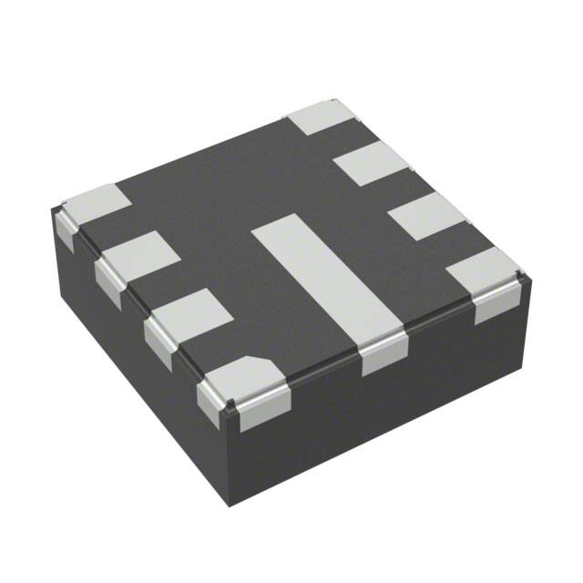


 工商网监
湘ICP备2023018690号
工商网监
湘ICP备2023018690号
