User's Guide
SNVU155A – June 2012 – Revised April 2013
AN-2264 LMR70503 Demo Board
1
Introduction
The LMR70503 is an inverting buck-boost converter with adjustable negative output voltage in a tiny 8bump DSBGA package (0.84 mm × 1.615 mm × 0.6 mm). Its unique control method is designed to
provide fast transient response, low output noise, high efficiency, and tight regulation in the smallest
possible PCB area. The LMR70503 has built in soft start, peak current limit, minimum switching frequency
limit, and Under Voltage Lock Out (UVLO), with no external compensation required. For ease of use, the
EN pin is referred to the IC ground instead of the negative output voltage. The LMR70503 is operating in
Discontinuous Conduction Mode (DCM) in light load. The minimum switching frequency is limited to 500
kHz to avoid audio frequency interference to other systems. Very small total solution size can be achieved
with the tiny footprint of the LMR70503 and the low external component count.
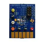
Top View
Bottom View
Figure 1. LMR70503 Demo Board
WEBENCH is a registered trademark of Texas Instruments.
All other trademarks are the property of their respective owners.
SNVU155A – June 2012 – Revised April 2013
Submit Documentation Feedback
AN-2264 LMR70503 Demo Board
Copyright © 2012–2013, Texas Instruments Incorporated
1
�LMR70503 Demo Board Schematic
2
www.ti.com
LMR70503 Demo Board Schematic
SW
D2
Cin2
(NC)
L1
D1
VIN
VIN
SW
Cin1
VOUT
B1
VOUT
Cff
EN
FB
Co2
B2
LMR70503
U1
R6
EN
Co1
D1
R1
R2
R3
R4
R5
J1
A2
R7
GND
Rt
C1
GND
C2
A1
VREF
Figure 2. LMR70503 Demo Board Schematic
3
LMR70503 Features
•
•
•
•
•
•
•
•
•
•
•
4
Tiny 8-Bump DSBGA Package: 0.84 mm × 1.615 mm × 0.6 mm
2.8 V to 5.5 V Input Voltage Range
Adjustable Output Voltage: -0.9 V to -5.5 V
320 mA Switch Current Limit
500 kHz Minimum Switching Frequency
Ground Referred Enable Input
Under Voltage Lock Out (UVLO)
No External Compensation
Internal Soft Start
1 μA Shutdown Supply Current
WEBENCH® Enabled
Selecting the Output Voltage
One of five output voltages can be selected by J1. The default setting is J1 open and the output voltage is
-5.0 V, set by resistor divider R1 and Rt:
VOUT = – VREF * R1 / Rt
(1)
When one of the four positions of J1 is connected, the resistor connected between this position and VOUT
is paralleled with R1 to provide a lower magnitude output voltage. Output voltages of -3.3 V, -2.5 V, -1.5 V
and -0.9 V can be selected by J1, as shown in Figure 1 and Figure 2.
Output voltage other than these five preset values can be achieved by replacing R1 and keep J1 open:
R1 = Rt * |VOUT| / VREF
(2)
where VREF is typically 1.19 Vand Rt is 100 kΩ. Rt can be selected between 20 kΩ and 100 kΩ.
2
AN-2264 LMR70503 Demo Board
SNVU155A – June 2012 – Revised April 2013
Submit Documentation Feedback
Copyright © 2012–2013, Texas Instruments Incorporated
�Operation Description
www.ti.com
5
Operation Description
The LMR70503 controller incorporates a unique peak current mode control method with a minimum
switching frequency limit. With fixed peak current limit, the switching frequency decreases with decreased
load current. At light load, the switching frequency will decrease to the audible frequency range, which is
not acceptable in many applications. The LMR70503 is designed to operate with peak current mode
control and limit the switching frequency to 500 kHz (typical) minimum, to avoid audible frequency
interference. At light load, when the switching frequency drops to the minimum, the inductor current limit is
reduced instead of frequency to maintain regulation. The LMR70503 also incorporates an internal dummy
load to maintain output regulation in the minimum ON-time (TON-MIN) condition. The maximum load the
LMR70503 can provide is limited by the maximum peak inductor current and the minimum off time
(TOFF_MIN) of the high side switch. The maximum load varies with input voltage, output voltage and the
inductor value. For more details on the LMR70503 operation, see LMR70503 SIMPLE SWITCHER BuckBoost Converter For Negative Output Voltage in DSBGA (SNVS850).
6
Enable and Disable
The LMR70503 features an enable (EN) pin and associated comparator to allow the user to easily
sequence the LMR70503 from an external voltage rail, or to manually set the input UVLO threshold.
Enable threshold levels are referred to the LMR70503 ground, instead of the lowest potential: the negative
output voltage. It is important to ensure that a valid input voltage (2.8 V ≤ VIN≤ 5.5 V) is present on the VIN
pin before the EN input is asserted. Also, the voltage on the EN pin must always be less than VIN. This
applies to both static and dynamic operation, and during start up and shut down sequences. The demo
board includes a resistor divider (R6 and R7) to pull EN pin up to half of VIN. The LMR70503 will be
enabled when VIN is higher than the UVLO level (typically 2.55 V with 0.13 V hysteresis band). Use the EN
post to control the EN pin externally.
7
Inductor and Diode
The inductor and diode selected on the demo board are optimized for very small total solution size. Larger
size inductor and diode can improve overall efficiency if size constraints allow. Bigger footprints are
provided for customer convenience.
8
Soft Start and Soft Off
The soft start action is inherent with the maximum peak current limit and the minimum off time. During
start up, the inductor current rises to the maximum peak current limit, then the high-side switch is turned
off for TOFF-MIN to let the inductor current charge the output capacitor(s). Then the high-side turns on to
repeat the cycle. After the output voltage is charged to the regulation level, the LMR70503 will operate in
steady state. The soft start time will be longer with more output capacitance, lower supply voltage VIN, and
more loading during start up. When shutdown, the LMR70503 incorporates an output voltage discharge
feature to bring the output voltage to zero volts, regardless of the load current.
9
Quick Setup Procedures
Step 1: Connect a power supply to VIN terminals
Step 2: Connect a load to VOUT terminals
Step 3: EN terminal can be left floating for normal operation. It can be connected to external signal for
sequencing.
Step 4: Set VIN = 5V, with 0A load applied, check VOUT with a voltmeter. Nominal -5 V
Step 5: Apply a 50mA load and check VOUT. Nominal -5 V
SNVU155A – June 2012 – Revised April 2013
Submit Documentation Feedback
AN-2264 LMR70503 Demo Board
Copyright © 2012–2013, Texas Instruments Incorporated
3
�Edge Connector
10
www.ti.com
Edge Connector
Figure 3 shows net names of the edge connector pins. The top side of the edge connector is connected to
the power traces of the LMR70503 demo board. The bottom side are signal pins. The VINS, VOUTS and
GNDS pins are sensing pins for VIN, VOUT and ground respectively. The sensing pins are connected to the
power nets via net ties close to the IC. They are designed for more accurate efficiency measurement
when edge connector is used. Additional voltage drops on the edge connector are bypassed if efficiency is
measured by:
EN
SW
VOUTS
GNDS
GNDS
VINS
(3)
VIN
VIN
GND
GND
VOUT
VOUT
IOUT × (VOUTS – GNDS) / (IIN × (VINS – GNDS))
Figure 3. Edge Connector
11
LMR70503 Bill of Materials
VIN = 2.8 V to 5.5 V, VOUT has options of -0.9 V, -1.5 V, -2.5 V, -3.3 V, and -5.0 V. Optimized for minimum
solution size.
Table 1. Bill of Materials
4
Designator
Value
Case Size
Manufacturer
Manufacturer P/N
U1
Inverting Buck-Boost
8-bump DSBGA
Texas Instruments
LMR70503
CIN1
10 µF 10 V X5R
0603
TDK
C1608X5R1A106M
CO1, CO2
22 µF 6.3 V X5R
0603
TDK
C1608X5R0J226M
Cff
10PF 50V 5% NP0
0402
Murata
GRM1555C1H100JZ01D
D
Schottky 30 V 500 mA
SOD882
NXP Semi
PMEG3005EL
L
6.8 µH, 0.76 A 362 mΩ
2.0*2.0*1.2mm
TDK
VLS2012ET-6R8M
Rt
100 kΩ, 1%, 0.063W
0402
Vishay Dale
CRCW0402100KFKED
R1, R3
422 kΩ, 1%, 0.063W
0402
Vishay Dale
CRCW0402422KFKED
R2
820 kΩ, 5%, 0.063W
0402
Vishay Dale
CRCW0402820KFKED
R4
180 kΩ 1/16W 1%
0402
Vishay Dale
CRCW0402180KFKED
R5
93.1 kΩ, 1%, 0.063W
0402
Vishay Dale
CRCW040293K1FKED
R6, R7
20 kΩ, 5%, 0.063W
0402
Vishay Dale
CRCW040220K0JNED
AN-2264 LMR70503 Demo Board
SNVU155A – June 2012 – Revised April 2013
Submit Documentation Feedback
Copyright © 2012–2013, Texas Instruments Incorporated
�Typical Performance Characteristics
www.ti.com
12
Typical Performance Characteristics
Unless otherwise specified, the following conditions apply: VIN = 3.3 V, VOUT = -5.0 V, VEN = 1.8 V, CIN =
10 µF, 6.3 V, X5R ceramic capacitor; COUT = 2 × 22 µF, 6.3 V, X5R ceramic capacitor; L = 6.8 µH
(VLS2012ET-6R8M); TAMBIENT = 25 °C.
Efficiency, VOUT = -5.0 V
Output Regulation, VOUT = -5.0 V
80
5.10
EFFICIENCY (%)
70
60
50
VIN = 2.8V
VIN = 3.3V
VIN = 4.0V
VIN = 5.0V
VIN = 5.5V
40
|VOUT| REGULATION (V)
5.08
5.06
5.04
5.02
5.00
4.99
VIN = 2.8V
VIN = 3.3V
VIN = 4.0V
VIN = 5.0V
VIN = 5.5V
4.96
4.95
4.92
30
4.90
0 10 20 30 40 50 60 70 80 90 100
LOAD (mA)
0 10 20 30 40 50 60 70 80 90 100
LOAD (mA)
Efficiency, VOUT = -3.3 V
Output Regulation, VOUT = -3.3 V
3.40
80
EFFICIENCY (%)
60
50
VIN = 2.8V
VIN = 3.3V
VIN = 4.0V
VIN = 5.0V
VIN = 5.5V
40
|VOUT| REGULATION (V)
3.38
70
3.36
3.34
3.32
3.30
3.28
VIN = 2.8V
VIN = 3.3V
VIN = 4.0V
VIN = 5.0V
VIN = 5.5V
3.26
3.24
3.22
30
3.20
0
20
40
60
80
LOAD (A)
100 120 140
0
SNVU155A – June 2012 – Revised April 2013
Submit Documentation Feedback
20
40
60 80 100 120 140
LOAD (mA)
AN-2264 LMR70503 Demo Board
Copyright © 2012–2013, Texas Instruments Incorporated
5
�Typical Performance Characteristics
www.ti.com
Efficiency, VOUT = -2.5 V
Output Regulation, VOUT = -2.5 V
80
2.60
|VOUT| REGULATION (V)
2.58
EFFICIENCY (%)
70
60
50
VIN = 2.8V
VIN = 3.3V
VIN = 4.0V
VIN = 5.0V
VIN = 5.5V
40
2.56
2.54
2.52
2.50
2.48
VIN = 2.8V
VIN = 3.3V
VIN = 4.0V
VIN = 5.0V
VIN = 5.5V
2.46
2.44
2.42
30
2.40
0
30
60
90
120
LOAD (mA)
150
180
0
Efficiency, VOUT = -1.5 V
20 40 60 80 100 120 140 160 180
LOAD (mA)
Output Regulation, VOUT = -1.5 V
1.60
80
1.58
|VOUT| REGULAITON (V)
EFFICIENCY (%)
70
60
50
VIN = 2.8V
VIN = 3.3V
VIN = 4.0V
VIN = 5.0V
VIN = 5.5V
40
1.56
1.54
1.52
1.50
1.48
VIN = 2.8V
VIN = 3.3V
VIN = 4.0V
VIN = 5.0V
VIN = 5.5V
1.46
1.44
1.42
30
1.40
0
30
60
90 120 150 180 210
LOAD (mA)
0
Efficiency, VOUT = -0.9 V
30
60
90 120 150 180 210
LOAD (mA)
Output Regulation, VOUT = -0.9 V
1.00
80
0.98
|VOUT| REGULATION (V)
EFFICIENCY (%)
70
60
50
VIN = 2.8V
VIN = 3.3V
VIN = 4.0V
VIN = 5.0V
VIN = 5.5V
40
0.96
0.94
0.92
0.90
0.88
VIN = 2.8V
VIN = 3.3V
VIN = 4.0V
VIN = 5.0V
VIN = 5.5V
0.86
0.84
0.82
30
0.80
0
6
50
100
150
LOAD (mA)
200
250
0
AN-2264 LMR70503 Demo Board
50
100
150
LOAD (mA)
200
250
SNVU155A – June 2012 – Revised April 2013
Submit Documentation Feedback
Copyright © 2012–2013, Texas Instruments Incorporated
�Typical Performance Characteristics
www.ti.com
Minimum Switching Frequency
MAX LOADING (mA)
200
150
100
VOUT = -5V
VOUT = -3.3V
VOUT = -2.5V
VOUT = -1.5V
VOUT = -0.9V
50
0
2.5
3.0
3.5
4.0
4.5
VIN (V)
5.0
5.5
MINIMUM SWITCHING FREQUENCY (kHz)
Maximum Load Current
250
600
Temp = -40°C
Temp = 25°C
Temp = 125°C
580
560
540
520
500
480
460
2.5
Enable Thresholds
3.0
3.5
4.0 4.5
VIN (V)
SOFT START TIME (NO LOAD) ( s)
EN THRESHOLDS (V)
1.1
1.0
0.9
0.8
Rising TH -40°C
Falling TH -40°C
Rising TH 25°C
Falling TH 25°C
Rising TH 125°C
Falling TH 125°C
0.6
0.5
0.4
2.5
3.0
3.5
5.5
Soft Start Time (No Load)
800
0.7
5.0
4.0
4.5
VIN (V)
5.0
Vout = -5.0V
Vout = -3.3V
Vout = -2.5V
Vout = -1.5V
Vout = -0.9V
700
600
500
400
300
200
100
0
5.5
2.5
Soft Start And Soft Off Waveform
VIN = 5.0 V, VOUT = -5.0 V, No Load
3.0
3.5
4.0
4.5
VIN (V)
5.0
Soft Start And Soft Off Waveform
VIN = 5.0 V, VOUT = -5.0 V, Load = 50 Ω
VSW
2V/Div
VSW
2V/Div
EN
1V/Div
EN
1V/Div
VOUT
IL
1V/Div
100 mA/Div
5.5
VOUT
IL
500 µs/Div
SNVU155A – June 2012 – Revised April 2013
Submit Documentation Feedback
1V/Div
100 mA/Div
500 µs/Div
AN-2264 LMR70503 Demo Board
Copyright © 2012–2013, Texas Instruments Incorporated
7
�Demo Board Layout
www.ti.com
Typical Switching Waveform
VIN = 5.0 V, VOUT = -5.0 V, No Load
Typical Switching Waveform
VIN = 5.0 V, VOUT = -5.0 V, IOUT = 70 mA
5V/Div
VSW
VSW
5V/Div
10 mV/Div, AC coupled
VOUT
VOUT
5 mV/Div
AC coupled
200 mA/Div
IL
IL
200 mA/Div
2 µs/Div
13
2 µs/Div
Demo Board Layout
The LMR70503 Demo Board is a four layer board with two internal ground planes. The layout of the top
and bottom layers is shown in the following figures.
Figure 4. Top Layer
8
AN-2264 LMR70503 Demo Board
SNVU155A – June 2012 – Revised April 2013
Submit Documentation Feedback
Copyright © 2012–2013, Texas Instruments Incorporated
�Demo Board Layout
www.ti.com
Figure 5. Top Overlay
Figure 6. Bottom Layer
SNVU155A – June 2012 – Revised April 2013
Submit Documentation Feedback
AN-2264 LMR70503 Demo Board
Copyright © 2012–2013, Texas Instruments Incorporated
9
�Demo Board Layout
www.ti.com
Figure 7. Bottom Overlay
10
AN-2264 LMR70503 Demo Board
SNVU155A – June 2012 – Revised April 2013
Submit Documentation Feedback
Copyright © 2012–2013, Texas Instruments Incorporated
�IMPORTANT NOTICE
Texas Instruments Incorporated and its subsidiaries (TI) reserve the right to make corrections, enhancements, improvements and other
changes to its semiconductor products and services per JESD46, latest issue, and to discontinue any product or service per JESD48, latest
issue. Buyers should obtain the latest relevant information before placing orders and should verify that such information is current and
complete. All semiconductor products (also referred to herein as “components”) are sold subject to TI’s terms and conditions of sale
supplied at the time of order acknowledgment.
TI warrants performance of its components to the specifications applicable at the time of sale, in accordance with the warranty in TI’s terms
and conditions of sale of semiconductor products. Testing and other quality control techniques are used to the extent TI deems necessary
to support this warranty. Except where mandated by applicable law, testing of all parameters of each component is not necessarily
performed.
TI assumes no liability for applications assistance or the design of Buyers’ products. Buyers are responsible for their products and
applications using TI components. To minimize the risks associated with Buyers’ products and applications, Buyers should provide
adequate design and operating safeguards.
TI does not warrant or represent that any license, either express or implied, is granted under any patent right, copyright, mask work right, or
other intellectual property right relating to any combination, machine, or process in which TI components or services are used. Information
published by TI regarding third-party products or services does not constitute a license to use such products or services or a warranty or
endorsement thereof. Use of such information may require a license from a third party under the patents or other intellectual property of the
third party, or a license from TI under the patents or other intellectual property of TI.
Reproduction of significant portions of TI information in TI data books or data sheets is permissible only if reproduction is without alteration
and is accompanied by all associated warranties, conditions, limitations, and notices. TI is not responsible or liable for such altered
documentation. Information of third parties may be subject to additional restrictions.
Resale of TI components or services with statements different from or beyond the parameters stated by TI for that component or service
voids all express and any implied warranties for the associated TI component or service and is an unfair and deceptive business practice.
TI is not responsible or liable for any such statements.
Buyer acknowledges and agrees that it is solely responsible for compliance with all legal, regulatory and safety-related requirements
concerning its products, and any use of TI components in its applications, notwithstanding any applications-related information or support
that may be provided by TI. Buyer represents and agrees that it has all the necessary expertise to create and implement safeguards which
anticipate dangerous consequences of failures, monitor failures and their consequences, lessen the likelihood of failures that might cause
harm and take appropriate remedial actions. Buyer will fully indemnify TI and its representatives against any damages arising out of the use
of any TI components in safety-critical applications.
In some cases, TI components may be promoted specifically to facilitate safety-related applications. With such components, TI’s goal is to
help enable customers to design and create their own end-product solutions that meet applicable functional safety standards and
requirements. Nonetheless, such components are subject to these terms.
No TI components are authorized for use in FDA Class III (or similar life-critical medical equipment) unless authorized officers of the parties
have executed a special agreement specifically governing such use.
Only those TI components which TI has specifically designated as military grade or “enhanced plastic” are designed and intended for use in
military/aerospace applications or environments. Buyer acknowledges and agrees that any military or aerospace use of TI components
which have not been so designated is solely at the Buyer's risk, and that Buyer is solely responsible for compliance with all legal and
regulatory requirements in connection with such use.
TI has specifically designated certain components as meeting ISO/TS16949 requirements, mainly for automotive use. In any case of use of
non-designated products, TI will not be responsible for any failure to meet ISO/TS16949.
Products
Applications
Audio
www.ti.com/audio
Automotive and Transportation
www.ti.com/automotive
Amplifiers
amplifier.ti.com
Communications and Telecom
www.ti.com/communications
Data Converters
dataconverter.ti.com
Computers and Peripherals
www.ti.com/computers
DLP® Products
www.dlp.com
Consumer Electronics
www.ti.com/consumer-apps
DSP
dsp.ti.com
Energy and Lighting
www.ti.com/energy
Clocks and Timers
www.ti.com/clocks
Industrial
www.ti.com/industrial
Interface
interface.ti.com
Medical
www.ti.com/medical
Logic
logic.ti.com
Security
www.ti.com/security
Power Mgmt
power.ti.com
Space, Avionics and Defense
www.ti.com/space-avionics-defense
Microcontrollers
microcontroller.ti.com
Video and Imaging
www.ti.com/video
RFID
www.ti-rfid.com
OMAP Applications Processors
www.ti.com/omap
TI E2E Community
e2e.ti.com
Wireless Connectivity
www.ti.com/wirelessconnectivity
Mailing Address: Texas Instruments, Post Office Box 655303, Dallas, Texas 75265
Copyright © 2013, Texas Instruments Incorporated
�


 工商网监
湘ICP备2023018690号
工商网监
湘ICP备2023018690号
