LMS1585A , LMS1587
www.ti.com
SNVS061G – MONTH 2003 – REVISED JULY 2013
LMS1585A 5A/LMS1587 5A and 3A Low Dropout Fast Response Regulators
Check for Samples: LMS1585A , LMS1587
FEATURES
DESCRIPTION
• Fast Transient Response
• Available in Adjustable, 1.5V, and 3.3V
versions
• Current Limiting and Thermal Protection
• Commercial Temp. Tange: 0°C to 125°C
• Industrial Temp. Range: −40°C to 125°C
• Line Regulation 0.005% (typical)
• Load Regulation 0.05% (typical)
• Direct Replacement for LT® 1585A/87
The LMS1585A and LMS1587 are low dropout
positive regulators with output load current of 5A and
3A respectively. Their low dropout voltage (1.2V) and
fast transient response make them an excellent
solution for low voltage microprocessor applications.
1
234
APPLICATIONS
•
•
•
•
Pentium® processor supplies
PowerPC® supplies
Other microprocessor supplies
Low voltage logic supplies
The LMS1585A/87 are available in adjustable
versions, which can set the output voltage with only
two external resistors. In addition, they are also
available in 1.5V and 3.3V fixed voltage versions (1).
The LMS1585A/87 circuits include a zener trimmed
bandgap reference, current limiting and thermal
shutdown. The LMS1585A/87 series are available in
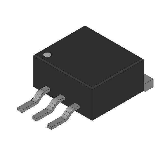
KTT (TO-263) and NDE (TO-220) packages.
(1)
Consult factory for other fixed voltage options.
Typical Application
VIN �4.75V
3.3V
3A, 5A
LMS1585A/87-3.3
+
+
C1
10 µF
C2*
10 µF
* Required for Stability
VOUT
INPUT
OUTPUT
ADJ/GND
Figure 1. NDE (TO-220)
(Top View)
INPUT
Tab is
VOUT
OUTPUT
ADJ/GND
Figure 2. KTT (TO-263)
(Top View)
1
2
3
4
Please be aware that an important notice concerning availability, standard warranty, and use in critical applications of
Texas Instruments semiconductor products and disclaimers thereto appears at the end of this data sheet.
PowerPC is a registered trademark of IBM.
Pentium is a registered trademark of Intel Corporation.
LT is a registered trademark of Linear Technology.
PRODUCTION DATA information is current as of publication date.
Products conform to specifications per the terms of the Texas
Instruments standard warranty. Production processing does not
necessarily include testing of all parameters.
Copyright © 2003–2013, Texas Instruments Incorporated
�LMS1585A , LMS1587
SNVS061G – MONTH 2003 – REVISED JULY 2013
www.ti.com
VIN
Thermal
Limit
VOUT
Substrate
GND (Fixed Output)
tADJ. (Adjustable Output)ttt
Table 1. LMS1585A/LMS1587 Device Options
Part Number
Output Voltage
LMS1585AIS-1.5
1.5V
LMS1585AIS-3.3
3.3V
LMS1585ACS-ADJ
Adjustable
LMS1585ACS-1.5
1.5V
LMS1585ACS-3.3
3.3V
LMS1585ACT-1.5
1.5V
LMS1585ACT-3.3
3.3V
LMS1587IS-ADJ
Adjustable
LMS1587IS-1.5
1.5V
LMS1587IS-3.3
3.3V
LMS1587CS-ADJ
Adjustable
LMS1587CS-3.3
3.3V
LMS1587CS-1.5
1.5V
LMS1587IT-1.5
1.5V
LMS1587CT-ADJ
Adjustable
LMS1587CT-3.3
3.3V
Operating
Temperature
Package Drawing
Package Type
Output Current
-40°C to 125°C
KTT
TO-263
5A
NDE
TO-220
5A
KTT
TO-263
0°C to 125°C
–40°C to 125°C
0°C to 125°C
3A
–40°C to 125C
0°C to 125°C
NDE
TO-220
These devices have limited built-in ESD protection. The leads should be shorted together or the device placed in conductive foam
during storage or handling to prevent electrostatic damage to the MOS gates.
2
Submit Documentation Feedback
Copyright © 2003–2013, Texas Instruments Incorporated
Product Folder Links: LMS1585A LMS1587
�LMS1585A , LMS1587
www.ti.com
SNVS061G – MONTH 2003 – REVISED JULY 2013
ABSOLUTE MAXIMUM RATINGS (1) (2)
Maximum Input to Output Voltage (VIN to GND)
Power Dissipation
13V
(3)
Internally Limited
Junction Temperature (TJ) (3)
150˚C
Storage Temperature Range
-65˚C to 150˚C
Lead Temperature
260˚C, 10 sec
ESD Tolerance (4)
(1)
(2)
(3)
(4)
2000V
Absolute Maximum Ratings indicate limits beyond which damage to the device may occur. Operating Ratings indicate conditions for
which the device is intended to be functional, but specific performance is not ensured. For ensured specifications and the test
conditions, see the Electrical Characteristics.
If Military/Aerospace specified devices are required, please contact the TI Sales Office/ Distributors for availability and specifications.
The maximum power dissipation is a function of TJ(max) , θJA, and TA. The maximum allowable power dissipation at any ambient
temperature is PD = (TJ(max)–T A)/θJA. All numbers apply for packages soldered directly into a PC board.
For testing purposes, ESD was applied using human body model, 1.5 kΩ in series with 100 pF.
Copyright © 2003–2013, Texas Instruments Incorporated
Product Folder Links: LMS1585A LMS1587
Submit Documentation Feedback
3
�LMS1585A , LMS1587
SNVS061G – MONTH 2003 – REVISED JULY 2013
www.ti.com
ELECTRICAL CHARACTERISTICS
Typicals and limits appearing in normal type apply for TJ = 25˚C. Limits appearing in Boldface type apply over the entire
junction temperature range for operation, 0˚C to 125˚C for commercial grade and −40˚C to 125˚C for industrial grade.
Symbol
VREF
Reference Voltage
VOUT
Output Voltage
∆VOUT
Line Regulation
VIN−VOUT
4
(3)
Load Regulation (3)
∆VOUT
(1)
(2)
(3)
Parameter
Dropout Voltage
Min (1)
Typ (2)
Max (1)
Units
LMS1585A-ADJ
VIN−VOUT = 3V, IOUT = 10mA
10mA ≤ IOUT ≤ 5A, 1.5V ≤ VIN− VOUT ≤ 5.75V
1.238
1.225
1.250
1.250
1.262
1.275
V
V
LMS1587-ADJ
10mA ≤ IOUT ≤ 3A, 1.5V ≤ VIN−VOUT ≤ 5.75V
1.225
1.250
1.275
V
LMS1585A-1.5
IOUT = 0mA, VIN = 5V
0 ≤ IOUT ≤ 5A, 3V ≤ VIN ≤ 7V
1.485
1.470
1.500
1.515
1.530
V
V
LMS1585A-3.3
I OUT = 0mA, V IN = 5V
0 ≤ I OUT ≤ 5A, 4.75V ≤ V IN ≤ 7V
3.267
3.235
3.300
3.300
3.333
3.365
V
V
LMS1587-1.5
V IN = 5V, I OUT = 0mA, TJ = 25˚C
0≤ I OUT ≤ 3A, 3V ≤ VIN ≤ 7V
1.485
1.470
1.500
1.500
1.515
1.530
V
V
LMS1587-3.3
0 ≤ I OUT ≤ 3A, 4.75V ≤ VIN ≤ 7V
3.235
3.300
3.365
V
LMS1585A/87-ADJ
IOUT = 10mA, 2.75V ≤ V IN ≤ 7V
0.005
0.2
%
LMS1585A/87-3.3
I OUT = 0mA, 4.75V ≤ VIN ≤ 7V
0.005
0.2
%
LMS1585A/87-1.5
I OUT = 0mA, 3V ≤ VIN ≤ 7V
Conditions
0.005
0.2
%
LMS1585A-ADJ
VIN−VOUT = 3V, 10mA ≤ IOUT ≤ 5A
%
0.05
0.3
0.5
LMS1585A-1.5/LMS1585A-3.3
VIN = 5V, 0 ≤ IOUT ≤ 5A
0.05
0.05
0.3
0.5
%
LMS1587-ADJ
VIN−VOUT = 3V, 10mA ≤ IOUT ≤ 3A
0.05
0.05
0.3
0.5
%
LMS1587-1.5/LMS1587-3.3
VIN = 5V, 0 ≤ IOUT ≤ 3A
0.05
0.05
0.3
0.5
%
%
LMS1585A-ADJ/LMS1587-ADJ
∆VREF = 1%, IOUT = 3A
1.15
1.3
V
LMS1585A-3.3/LMS1587-3.3/
LMS1585A-1.5/LMS1587-1.5
∆VOUT = 1%, IOUT = 3A
1.15
1.3
V
LMS1585A-ADJ
∆VREF = 1%, IOUT = 5A
1.2
1.4
V
LMS1585A-1.5/LMS1585A-3.3
∆VOUT = 1%, IOUT = 5A
1.2
1.4
V
All limits are specified by testing or statistical analysis.
Typical Values represent the most likely parametric norm.
Load and line regulation are measured at constant junction temperature, and are ensured up to the maximum power dissipation of 30W.
Power dissipation is determined by the input/output differential and the output current. Ensured maximum power dissipation will not be
available over the full input/output range.
Submit Documentation Feedback
Copyright © 2003–2013, Texas Instruments Incorporated
Product Folder Links: LMS1585A LMS1587
�LMS1585A , LMS1587
www.ti.com
SNVS061G – MONTH 2003 – REVISED JULY 2013
ELECTRICAL CHARACTERISTICS (continued)
Typicals and limits appearing in normal type apply for TJ = 25˚C. Limits appearing in Boldface type apply over the entire
junction temperature range for operation, 0˚C to 125˚C for commercial grade and −40˚C to 125˚C for industrial grade.
ILIMIT
Current Limit
LMS1585A-ADJ/LMS1585A-3.3/LMS1585A-1.5
VIN−VOUT = 5.5V
5.0
6.6
A
LMS1587-ADJ/LMS1587-3.3/LMS1587-1.5
VIN−VOUT = 5.5V
3.1
4.3
A
Minimum Load
Current (4)
LMS1585A/87-ADJ
1.5V ≤ VIN−VOUT ≤ 5.75V
Quiescent Current
LMS1585A-3.3/LMS1587-3.3/
LMS1585A-1.5/LMS1587-1.5
VIN = 5V
Thermal Regulation
TA = 25˚C, 30ms Pulse
Ripple Rejection
LMS1585A-ADJ
fRIPPLE = 120Hz, VIN−VOUT = 3V,
IOUT = 5A, COUT = 25µF Tantalum
LMS1585A-1.5
fRIPPLE = 120Hz, COUT = 25µF
Tantalum, IOUT = 5A, VIN = 4.5V
7.0
13.0
mA
0.003
%/W
72
dB
dB
72
dB
LMS1587-ADJ
fRIPPLE = 120 Hz, VIN−VOUT = 3V, IOUT = 3A
COUT = 25 µF Tantalum
72
dB
72
dB
72
dB
Adjust Pin Current
60
55
10mA ≤ IOUT ≤ IFULLLOAD,
1.5V ≤ VIN−VOUT ≤ 5.75V (5)
Adjust Pin Current
mA
72
LMS1587-3.3
fRIPPLE = 120 Hz, COUT = 25µF Tantalum,
IOUT = 3A, VIN = 6.3V
Temperature Stability
(4)
(5)
10.0
LMS1585A-3.3
fRIPPLE = 120Hz, COUT = 25µF
Tantalum, IOUT = 5A, VIN = 6.3V
LMS1587-1.5
fRIPPLE = 120 Hz, COUT = 25µF Tantalum,
IOUT = 3A, VIN = 4.5V
60
2.0
120
µA
0.2
µA
0.5
%
Long Term Stability
TA = 125˚C, 1000Hrs
0.03
%
RMS Output Noise
(% of VOUT)
10Hz ≤ f ≤ 10kHz
0.003
%
Thermal Resistance
Junction-to-Case
3-Lead KTT (TO-263): Control/Output Section
3-Lead NDE (TO-220): Control/Output Section
0.65/2.7
0.65/2.7
*C/W
*C/W
The minimum output current required to maintain regulation.
IFULLLOAD is 5A for LMS1585A and 3A for LMS1587.
Copyright © 2003–2013, Texas Instruments Incorporated
Product Folder Links: LMS1585A LMS1587
Submit Documentation Feedback
5
�LMS1585A , LMS1587
SNVS061G – MONTH 2003 – REVISED JULY 2013
www.ti.com
APPLICATION NOTE
OUTPUT VOLTAGE
The adjustable version develops at 1.25V reference voltage, (VREF), between the output and the adjust terminal.
As shown in Figure 3, this voltage is applied across resistor R1 to generate a constant current I1. This constant
current then flows through R2. The resulting voltage drop across R2 adds to the reference voltage to sets the
desired output voltage.
The current IADJ from the adjustment terminal introduces an output error. But since it is small (120μA max), it
becomes negligible when R1 is in the 100Ω range.
For fixed voltage devices, R1 and R2 are integrated inside the devices.
VIN
VIN
VOUT
VOUT
ADJ
I1
VREF
R1
10 µF
10 µF
IADJ
R2
R2) + IADJR2
VOUT = VREF (1 + R2
R1
Figure 3. Basic Adjustable Regulator
6
Submit Documentation Feedback
Copyright © 2003–2013, Texas Instruments Incorporated
Product Folder Links: LMS1585A LMS1587
�PACKAGE OPTION ADDENDUM
www.ti.com
19-Apr-2022
PACKAGING INFORMATION
Orderable Device
Status
(1)
Package Type Package Pins Package
Drawing
Qty
Eco Plan
(2)
Lead finish/
Ball material
MSL Peak Temp
Op Temp (°C)
Device Marking
(3)
(4/5)
(6)
LMS1585ACS-1.5
NRND
DDPAK/
TO-263
KTT
3
45
Non-RoHS
& Green
Call TI
Level-3-235C-168 HR
0 to 125
LMS1585
ACS-1.5
LMS1585ACS-1.5/NOPB
ACTIVE
DDPAK/
TO-263
KTT
3
45
RoHS-Exempt
& Green
SN
Level-3-245C-168 HR
0 to 125
LMS1585
ACS-1.5
LMS1585ACS-3.3
NRND
DDPAK/
TO-263
KTT
3
45
Non-RoHS
& Green
Call TI
Level-3-235C-168 HR
0 to 125
LMS1585
ACS-3.3
LMS1585ACS-3.3/NOPB
ACTIVE
DDPAK/
TO-263
KTT
3
45
RoHS-Exempt
& Green
SN
Level-3-245C-168 HR
0 to 125
LMS1585
ACS-3.3
LMS1585ACSX-1.5/NOPB
ACTIVE
DDPAK/
TO-263
KTT
3
500
RoHS-Exempt
& Green
SN
Level-3-245C-168 HR
0 to 125
LMS1585
ACS-1.5
LMS1585ACSX-3.3/NOPB
ACTIVE
DDPAK/
TO-263
KTT
3
500
RoHS-Exempt
& Green
SN
Level-3-245C-168 HR
0 to 125
LMS1585
ACS-3.3
LMS1585ACSX-ADJ/NOPB
ACTIVE
DDPAK/
TO-263
KTT
3
500
RoHS-Exempt
& Green
SN
Level-3-245C-168 HR
0 to 125
LMS1585
ACS-ADJ
LMS1585ACT-1.5/NOPB
ACTIVE
TO-220
NDE
3
45
RoHS & Green
SN
Level-1-NA-UNLIM
0 to 125
LMS1585ACT
1.5
LMS1585ACT-3.3/NOPB
ACTIVE
TO-220
NDE
3
45
RoHS & Green
SN
Level-1-NA-UNLIM
0 to 125
LMS1585
ACT-3.3
LMS1585AIS-1.5
NRND
DDPAK/
TO-263
KTT
3
45
Non-RoHS
& Green
Call TI
Level-3-235C-168 HR
-40 to 125
LMS1585
AIS-1.5
LMS1585AIS-1.5/NOPB
ACTIVE
DDPAK/
TO-263
KTT
3
45
RoHS-Exempt
& Green
SN
Level-3-245C-168 HR
-40 to 125
LMS1585
AIS-1.5
LMS1585AIS-3.3/NOPB
ACTIVE
DDPAK/
TO-263
KTT
3
45
RoHS-Exempt
& Green
SN
Level-3-245C-168 HR
-40 to 125
LMS1585
AIS-3.3
LMS1585AISX-3.3/NO
ACTIVE
DDPAK/
TO-263
KTT
3
500
RoHS-Exempt
& Green
SN
Level-3-245C-168 HR
-40 to 125
LMS1585
AIS-3.3
LMS1587CS-1.5/NOPB
ACTIVE
DDPAK/
TO-263
KTT
3
45
RoHS-Exempt
& Green
SN
Level-3-245C-168 HR
0 to 125
LMS1587
CS-1.5
LMS1587CS-3.3/NOPB
ACTIVE
DDPAK/
TO-263
KTT
3
45
RoHS-Exempt
& Green
SN
Level-3-245C-168 HR
0 to 125
LMS1587
CS-3.3
LMS1587CS-ADJ
NRND
DDPAK/
TO-263
KTT
3
45
Non-RoHS
& Green
Call TI
Level-3-235C-168 HR
0 to 125
LMS1587
CS-ADJ
Addendum-Page 1
Samples
�PACKAGE OPTION ADDENDUM
www.ti.com
Orderable Device
19-Apr-2022
Status
(1)
Package Type Package Pins Package
Drawing
Qty
Eco Plan
(2)
Lead finish/
Ball material
MSL Peak Temp
Op Temp (°C)
Device Marking
(3)
(4/5)
(6)
LMS1587CS-ADJ/NOPB
ACTIVE
DDPAK/
TO-263
KTT
3
45
RoHS-Exempt
& Green
SN
Level-3-245C-168 HR
0 to 125
LMS1587
CS-ADJ
LMS1587CSX-1.5/NOPB
ACTIVE
DDPAK/
TO-263
KTT
3
500
RoHS-Exempt
& Green
SN
Level-3-245C-168 HR
0 to 125
LMS1587
CS-1.5
LMS1587CSX-3.3/NOPB
ACTIVE
DDPAK/
TO-263
KTT
3
500
RoHS-Exempt
& Green
SN
Level-3-245C-168 HR
0 to 125
LMS1587
CS-3.3
LMS1587CSX-ADJ/NOPB
ACTIVE
DDPAK/
TO-263
KTT
3
500
RoHS-Exempt
& Green
SN
Level-3-245C-168 HR
0 to 125
LMS1587
CS-ADJ
LMS1587CT-3.3
NRND
TO-220
NDE
3
45
Non-RoHS
& Green
Call TI
Level-1-NA-UNLIM
0 to 125
LMS1587
CT-3.3
LMS1587CT-3.3/NOPB
ACTIVE
TO-220
NDE
3
45
RoHS & Green
SN
Level-1-NA-UNLIM
0 to 125
LMS1587
CT-3.3
LMS1587CT-ADJ/NOPB
ACTIVE
TO-220
NDE
3
45
RoHS & Green
SN
Level-1-NA-UNLIM
0 to 125
LMS1587
CT-ADJ
LMS1587IS-1.5
NRND
DDPAK/
TO-263
KTT
3
45
Non-RoHS
& Green
Call TI
Level-3-235C-168 HR
-40 to 125
LMS1587
IS-1.5
LMS1587IS-1.5/NOPB
ACTIVE
DDPAK/
TO-263
KTT
3
45
RoHS-Exempt
& Green
SN
Level-3-245C-168 HR
-40 to 125
LMS1587
IS-1.5
LMS1587IS-3.3
NRND
DDPAK/
TO-263
KTT
3
45
Non-RoHS
& Green
Call TI
Level-3-235C-168 HR
-40 to 125
LMS1587
IS-3.3
LMS1587IS-3.3/NOPB
ACTIVE
DDPAK/
TO-263
KTT
3
45
RoHS-Exempt
& Green
SN
Level-3-245C-168 HR
-40 to 125
LMS1587
IS-3.3
LMS1587IS-ADJ
NRND
DDPAK/
TO-263
KTT
3
45
Non-RoHS
& Green
Call TI
Level-3-235C-168 HR
-40 to 125
LMS1587
IS-ADJ
LMS1587IS-ADJ/NOPB
ACTIVE
DDPAK/
TO-263
KTT
3
45
RoHS-Exempt
& Green
SN
Level-3-245C-168 HR
-40 to 125
LMS1587
IS-ADJ
LMS1587ISX-3.3/NOPB
ACTIVE
DDPAK/
TO-263
KTT
3
500
RoHS-Exempt
& Green
SN
Level-3-245C-168 HR
-40 to 125
LMS1587
IS-3.3
LMS1587ISX-ADJ/NOPB
ACTIVE
DDPAK/
TO-263
KTT
3
500
RoHS-Exempt
& Green
SN
Level-3-245C-168 HR
-40 to 125
LMS1587
IS-ADJ
LMS1587IT-1.5/NOPB
ACTIVE
TO-220
NDE
3
45
RoHS & Green
SN
Level-1-NA-UNLIM
-40 to 125
LMS1587
IT-1.5
(1)
The marketing status values are defined as follows:
ACTIVE: Product device recommended for new designs.
LIFEBUY: TI has announced that the device will be discontinued, and a lifetime-buy period is in effect.
Addendum-Page 2
Samples
�PACKAGE OPTION ADDENDUM
www.ti.com
19-Apr-2022
NRND: Not recommended for new designs. Device is in production to support existing customers, but TI does not recommend using this part in a new design.
PREVIEW: Device has been announced but is not in production. Samples may or may not be available.
OBSOLETE: TI has discontinued the production of the device.
(2)
RoHS: TI defines "RoHS" to mean semiconductor products that are compliant with the current EU RoHS requirements for all 10 RoHS substances, including the requirement that RoHS substance
do not exceed 0.1% by weight in homogeneous materials. Where designed to be soldered at high temperatures, "RoHS" products are suitable for use in specified lead-free processes. TI may
reference these types of products as "Pb-Free".
RoHS Exempt: TI defines "RoHS Exempt" to mean products that contain lead but are compliant with EU RoHS pursuant to a specific EU RoHS exemption.
Green: TI defines "Green" to mean the content of Chlorine (Cl) and Bromine (Br) based flame retardants meet JS709B low halogen requirements of


 工商网监
湘ICP备2023018690号
工商网监
湘ICP备2023018690号
