October 13, 2011
LMV7251/LMV7255
1.8V Low Voltage Comparator with Rail-to-Rail Input
General Description
Features
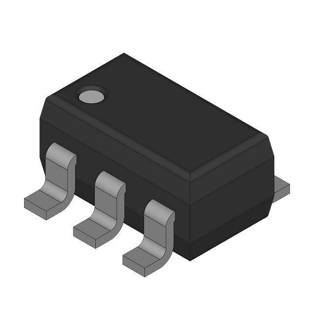
The LMV7251/LMV7255 are rail-to-rail input low voltage comparators, which can operate at supply voltage range of 1.8V
to 5.0V. The LMV7251/LMV7255 are available in space saving SC-70 or SOT23-5 packages. These comparators are
ideal for low voltage and space critical designs.
The LMV7251 features a push-pull output stage. This feature
allows operation with minimum power consumption when
driving a load.
The LMV7255 features an open drain output. This allows the
connection of an external resistor at the output. The output of
the comparator can be used as a level shifter.
The IC's are built with National Semiconductor's advance
Submicron Silicon-Gate BiCMOS process. The LMV7251/
LMV7255 have bipolar inputs for improved noise performance and CMOS outputs for better rail-to-rail output performance.
(VS = 1.8V, TA = 25°C, Typical values unless specified).
■ Single or Dual Supplies
1.8V to 5.0V
■ Low supply voltage
11µA
■ Ultra low supply current
14nA
■ Low input bias current
200pA
■ Low input offset current
+/−0.3mV
■ Low input offset voltage
670ns (20mV overdrive)
■ Response time
0.1V beyond rails
■ Input common mode voltage
Typical Circuit
Connection Diagram
Applications
■
■
■
■
Mobile communications
Laptops and PDA's
Battery powered electronics
General purpose low voltage applications
20005701
Top View
20005702
FIGURE 1. Threshold Detector
© 2011 National Semiconductor Corporation
200057
200057 Version 5 Revision 2
www.national.com
Print Date/Time: 2011/10/13 15:13:37
LMV7251/LMV7255 1.8V Low Voltage Comparator with Rail-to-Rail Input
OBSOLETE
�LMV7251/LMV7255
Wave Soldering (10 sec.)
Storage Temperature Range
Junction Temperature (Note 4)
Absolute Maximum Ratings (Note 1)
If Military/Aerospace specified devices are required,
please contact the National Semiconductor Sales Office/
Distributors for availability and specifications.
ESD Tolerance
Operating Ratings
1KV (Note 2)
200V (Note 6)
+/−Supply Voltage
5.5V
V+ +0.1V, V− −0.1V
VIN Differential
Supply Voltage (V+ - V−)
Voltage at Input/Output pins
Soldering Information
Infrared or Convection (20 sec.)
260°C
−65°C to +150°C
+150°C
(Note 1)
V+
Supply Voltage
Junction Temperature Range (Note
3)
Package Thermal Resisance (Note 3)
SOT23-5
SC-70
235°C
1.8V to 5.0V
−40°C to +85°C
325°C/W
265°C/W
1.8V Electrical Characteristics
Unless otherwise specified, all limits guaranteed for TJ = 25°C, V+ = 1.8V, V− = 0V. Boldface limits apply at the temperature
extremes.
Symbol
Parameter
VOS
Input Offset Voltage
TC VOS
Input Offset Average Drift
IB
IOS
Condition
VCM = 0.9V (Note 7)
Typ
(Note 4)
Limits
(Note 5)
Units
0.3
6
8
mV
max
10
uV/C
Input Bias Current
14
nA
Input Offset Current
200
pA
IS
Supply Current
11
15
17
ISC
Output Short Circuit Current
8
4
Sinking, VO = 0.9V
11.6
5
Sourcing, VO = 0.9V
(LMV7251 only)
µA
max
mA
min
ILEAKAGE
Output Leakage Current
VO = 1.8V
(LMV7255 only)
300
pA
VOH
Output Voltage High
IO = 1.5mA
(LMV7251 only)
1.72
1.675
V
min
VOL
Output Voltage Low
IO = −1.5mA
65
125
mV
max
VCM
Input Common Voltage Range
CMRR > 45 dB
1.9
V
max
−0.1
V
min
CMRR
Common Mode Rejection Ratio
0 < VCM < 1.8V
72
47
dB
min
PSRR
Power Supply Rejection Ratio
V+ = 1.8V to 5V
79
55
dB
min
www.national.com
2
200057 Version 5 Revision 2
Print Date/Time: 2011/10/13 15:13:37
�Unless otherwise specified, all limits guaranteed for TJ = 25°C, V+ = 1.8V, V− = 0V, VCM = 0.5V, VO = V+/2. Boldface limits apply
at the temperature extremes.
Symbol
tPHL
tPLH
Parameter
Propagation Delay
(High to Low)
Propagation Delay
(Low to High)
Condition
Typ
(Note 5)
Limits
(Note 6)
Units
Input Overdrive = 20mV
Load = 50pF//5kΩ
720
ns
Input Overdrive = 50mV
Load = 50pF//5kΩ
380
ns
Input Overdrive = 20mV
Load = 50pF//5kΩ
670
ns
Input Overdrive = 50mV
Load = 50pF//5kΩ
400
ns
2.7V Electrical Characteristics
Unless otherwise specified, all limits guaranteed for TJ = 25°C, V+ = 2.7V, V− = 0V. Boldface limits apply at the temperature
extremes.
Symbol
Parameter
Conditions
Typ
(Note 5)
Limits
(Note 6)
Units
0.03
6
8
mV
max
VOS
Input Offset Voltage
TC VOS
Input Offset Average Drift
10
µV/C
IB
Input Bias Current
15
nA
IOS
Input offset Current
210
IS
Supply Current
11
18
22
ISC
Output Short Circuit Current
Sourcing, VO = 1.35V
(LMV7251 only)
28
15
Sinking, VO = 1.35V
28
15
VCM = 1.35V (Note 7)
pA
µA
max
mA
ILEAKAGE
Output Leakage Current
VO = 2.7V,
(LMV7255 only)
320
pA
VOH
Output Voltage High
IO = 2mA
(LMV7251 only)
2.63
2.575
V
min
VOL
Output Voltage Low
IO = −2mA
61
125
mV
max
VCM
Input Common Voltage Range
CMRR > 45dB
2.8
V
max
−0.1
V
min
CMRR
Common Mode Rejection Ratio
0 < VCM < 2.7V
75
46
dB
min
PSRR
Power Supply Rejection Ratio
V+ = 1.8V to 5V
79
55
dB
min
3
200057 Version 5 Revision 2
Print Date/Time: 2011/10/13 15:13:37
www.national.com
LMV7251/LMV7255
1.8V AC Electrical Characteristics
�LMV7251/LMV7255
2.7V AC Electrical Characteristics
Unless otherwise specified, all limits guaranteed for TJ = 25°C, V+ = 2.7V, V− = 0V.Boldface limits apply at the temperature
extremes.
Symbol
tPHL
tPLH
Parameter
Propagation Delay
(High to Low)
Propagation Delay
(Low to High)
Condition
Typ
(Note 5)
Limits
(Note 6)
Units
Input Overdrive = 20mV
Load = 50pF//5kΩ
830
ns
Input Overdrive = 50mV
Load = 50pF//5kΩ
430
ns
Input Overdrive = 20mV
Load = 50pF//5kΩ
730
ns
Input Overdrive = 50mV
Load = 50pF//5kΩ
410
ns
5V Electrical Characteristics
Unless otherwise specified, all limits guaranteed for TJ = 25°C, V+ = 5V, V− = 0V. Boldface limits apply at the temperature extremes.
Symbol
Parameter
VOS
Input Offset Voltage
TC VOS
Input Offset Average Drift
IB
IOS
Conditions
VCM = 2.5V (Note 7)
Typ
(Note 5)
Limits
(Note 6)
Units
0.03
6
8
mV
max
10
µV/C
Input Bias Current
16
nA
Input Offset Current
220
pA
IS
Supply Current
12
20
25
ISC
Output Short Circuit Current
Sourcing, VO = 2.5V
(LMV7251 only)
82
50
Sinking, VO = 2.5V
78
50
µA
max
mA
min
ILEAKAGE
Output Leakage Current
VO = 5V,
(LMV7255 only)
375
pA
VOH
Output Voltage High
IO = 4mA
4.9
4.82
V
min
VOL
Output Voltage Low
IO = −4mA
90
180
mV
max
Note 1: Absolute Maximum Ratings indicate limits beyond which damage to the device may occur. Operating Ratings indicate conditions for which the device is
intended to be functional, but specific performance is not guaranteed. For guaranteed specifications and the test conditions, see the Electrical Characteristics.
Note 2: Human body model, 1.5kΩ in series with 100pF.
Note 3: The maximum power dissipation is a function of TJ(max), θJA, and TA. The maximum allowable power dissipation at any ambient temperature is
PD = (TJ(max) - TA)/θJA. All numbers apply for packages soldered directly into a PC board.
Note 4: Typical values represent the most likely parametric norm.
Note 5: All limits are guaranteed by testing or statistical analysis.
Note 6: Machine Model, 0Ω in series with 200pF.
Note 7: Offset Voltage average drift determined by dividing the change in VOS at temperature extremes into the total temperature change.
www.national.com
4
200057 Version 5 Revision 2
Print Date/Time: 2011/10/13 15:13:37
�LMV7251/LMV7255
Typical Performance Characteristics
(TA = 25°C, Unless otherwise specified).
Short Circuit Current vs. Supply Voltage
Supply Current vs. Supply Voltage
20005704
20005703
Output Voltage vs. Supply Voltage
Output Voltage vs. Supply Voltage
20005705
20005706
Output Voltage vs. Output Current @1.8V Supply Voltage
Output Voltage vs. Output Current @1.8V Supply Voltage
20005707
20005708
5
200057 Version 5 Revision 2
Print Date/Time: 2011/10/13 15:13:37
www.national.com
�LMV7251/LMV7255
Output Voltage vs. Output Current @2.7V Supply Voltage
Output Voltage vs. Output Current @2.7V Supply Voltage
20005709
20005710
Response Time for Various Input Overdrives - tPLH
Response Time for Various Input Overdrives - tPHL
20005711
20005712
Response Time for Various Input Overdrives - tPLH
Response Time for Various Input Overdrives - tPHL
20005713
www.national.com
20005714
6
200057 Version 5 Revision 2
Print Date/Time: 2011/10/13 15:13:37
�BASIC COMPARATORS
A comparator is quite often used to convert an analog signal
to a digital signal. The comparator compares an input voltage
(VIN) at the non-inverting pin to the reference voltage (VREF)
at the inverting pin. If VIN is less than VREF the output (V O) is
low (VOL). However, if VIN is greater than VREF, the output
voltage (VO) is high (VOH).
LMV7251
ΔVIN = VIN1- VIN2 = ((VREF (R1 + R2)) / R2) - ((VREF (R1 + R2)
- VCC R1) / R2) = VCC R1/ R2.
20005715
LMV7255
20005718
20005716
Input/Output
20005719
FIGURE 3. Non-Inverting Comparator Configuration —
LMV7251
For an inverting configured comparator, hysteresis can be
added with a three resistor network and positive feedback.
When input voltage (VIN) at the inverting node is less than
non-inverting node (VT), the output is high. The equivalent
circuit for the three resistor network is R1 in parallel with R3
and in series with R2. The lower threshold voltage VT1 is calculated by:
VT1 = ((VCC R2) / ((R1 R3) / (R1+ R3)) + R2)
When VIN is greater than VT, the output voltage is low. The
equivalent circuit for the three resistor network is R2 in parallel
with R3 and in series with R1. The upper threshold voltage
VT2 is calculated by:
VT2 = VCC ((R2 R3) / (R2 + R3)) / ((R1 + ((R2 R3) / (R2 + R3))
20005717
FIGURE 2. Basic Comparator
HYSTERESIS
The basic comparator configuration may oscillate or produce
a noisy output if the applied differential input is near the
comparator's input offset voltage. This tends to occur when
the voltage on the input is equal or very close to the other input
voltage. Adding hysteresis can prevent this problem. Hysteresis creates two switching thresholds (one for the rising
input voltage and the other for the falling input voltage). Hys-
7
200057 Version 5 Revision 2
Print Date/Time: 2011/10/13 15:13:37
www.national.com
LMV7251/LMV7255
teresis is the voltage difference between the two switching
thresholds. When both inputs are nearly equal, hysteresis
causes one input to effectively move quickly pass the other.
Thus, effectively moving the input out of region that oscillation
may occur.
Hysteresis can easily be added to a comparator in a non-inverting configuration with two resistors and positive feedback
Figure 3. The output will switch from low to high when VIN rises
up to VIN1, where VIN1 is calculated by
VIN1 = (VREF (R1 + R2))/ R2
The output will switch from high to low when VIN falls to VIN2,
where VIN2 is calculated by
VIN2 = (VREF (R1 + R2) - VCC R1) / R2
The Hysteresis is the difference between VIN1 and VIN2.
Application Info
�LMV7251/LMV7255
The hysteresis is defined as
INPUT STAGE
The LMV7251 and LMV7255 have rail-to-rail input stages.
The input common mode voltage range is from −100mV to
(VCC + 100mV).
ΔVIN = VT1 - VT2 = ((VCC R2) / ((R1 R3) / (R1+ R3)) + R2) –
(VCC ((R2 R3) / (R2 + R3)) / ((R1 + ((R2 R3) / (R2 + R3)))
OUTPUT STAGE
The LMV7251 has a push-pull CMOS output stage. Large
push-pull output drivers allows rail-to-rail output swings with
load currents in the miliampere range.
The LMV7255 has a open drain CMOS output stage. This requires an external pull-up resistor connected between the
positive supply voltage and the output. The external pull-up
resistor should be high enough resistance so to avoid excessive power dissipation. In addition, the pull-up resistor should
be low enough resistance to enable the comparator to switch
with the load circuitry connected.
POWER SUPPLY CONSIDERATIONS
The LMV7251/LMV7255 are well suited for many batterypowered applications. The LMV7251/LMV7255 can operate
from single power supply of +1.8V to +5V. The device typically
consumes only 11µA with a 2.7V supply. With a high power
supply rejection ratio (PSRR) of 79 dB (typical), the comparator is well suited for operating under conditions of a decaying
battery voltage.
Power supply decoupling is critical and improves stability.
Place decoupling capacitors 0.1µF as close as possible to the
V+ pin. For split supply applications, place decoupling capacitors 0.1µF on both the V+ and V− pins. The decoupling
capacitors will help keep the comparator from oscillating under various load conditions.
20005720
20005721
FIGURE 4. Inverting Configured Comparator — LMV7255
www.national.com
8
200057 Version 5 Revision 2
Print Date/Time: 2011/10/13 15:13:37
�Package
Ordering Info
Pkg Marking
Supplied As
NSC Drawing
5-Pin SOT23-5
LMV7251M5
C16A
1k Units Tape and Reel
MF05A
LMV7251M5X
C16A
3k units Tape and Reel
LMV7255M5
C18A
1k Units Tape and Reel
LMV7255M5X
C18A
3k units Tape and Reel
5-Pin SC-70
LMV7251M7
C17
1k Units Tape and Reel
LMV7251M7X
C17
3k units Tape and Reel
LMV7255M7
C19
1k Units Tape and Reel
LMV7255M7X
C19
3k units Tape and Reel
9
200057 Version 5 Revision 2
Print Date/Time: 2011/10/13 15:13:37
MAA05A
www.national.com
LMV7251/LMV7255
Ordering Information
�LMV7251/LMV7255
Physical Dimensions inches (millimeters) unless otherwise noted
5-Pin SC70-5
NS Package Number MAA05A
5-Pin SOT23-5
NS Package Number MF05A
www.national.com
10
200057 Version 5 Revision 2
Print Date/Time: 2011/10/13 15:13:37
�LMV7251/LMV7255
Notes
11
200057 Version 5 Revision 2
Print Date/Time: 2011/10/13 15:13:37
www.national.com
�LMV7251/LMV7255 1.8V Low Voltage Comparator with Rail-to-Rail Input
Notes
For more National Semiconductor product information and proven design tools, visit the following Web sites at:
www.national.com
Products
Design Support
Amplifiers
www.national.com/amplifiers
WEBENCH® Tools
www.national.com/webench
Audio
www.national.com/audio
App Notes
www.national.com/appnotes
Clock and Timing
www.national.com/timing
Reference Designs
www.national.com/refdesigns
Data Converters
www.national.com/adc
Samples
www.national.com/samples
Interface
www.national.com/interface
Eval Boards
www.national.com/evalboards
LVDS
www.national.com/lvds
Packaging
www.national.com/packaging
Power Management
www.national.com/power
Green Compliance
www.national.com/quality/green
Switching Regulators
www.national.com/switchers
Distributors
www.national.com/contacts
LDOs
www.national.com/ldo
Quality and Reliability
www.national.com/quality
LED Lighting
www.national.com/led
Feedback/Support
www.national.com/feedback
Voltage References
www.national.com/vref
Design Made Easy
www.national.com/easy
www.national.com/powerwise
Applications & Markets
www.national.com/solutions
Mil/Aero
www.national.com/milaero
PowerWise® Solutions
Serial Digital Interface (SDI) www.national.com/sdi
Temperature Sensors
www.national.com/tempsensors SolarMagic™
www.national.com/solarmagic
PLL/VCO
www.national.com/wireless
www.national.com/training
PowerWise® Design
University
THE CONTENTS OF THIS DOCUMENT ARE PROVIDED IN CONNECTION WITH NATIONAL SEMICONDUCTOR CORPORATION
(“NATIONAL”) PRODUCTS. NATIONAL MAKES NO REPRESENTATIONS OR WARRANTIES WITH RESPECT TO THE ACCURACY
OR COMPLETENESS OF THE CONTENTS OF THIS PUBLICATION AND RESERVES THE RIGHT TO MAKE CHANGES TO
SPECIFICATIONS AND PRODUCT DESCRIPTIONS AT ANY TIME WITHOUT NOTICE. NO LICENSE, WHETHER EXPRESS,
IMPLIED, ARISING BY ESTOPPEL OR OTHERWISE, TO ANY INTELLECTUAL PROPERTY RIGHTS IS GRANTED BY THIS
DOCUMENT.
TESTING AND OTHER QUALITY CONTROLS ARE USED TO THE EXTENT NATIONAL DEEMS NECESSARY TO SUPPORT
NATIONAL’S PRODUCT WARRANTY. EXCEPT WHERE MANDATED BY GOVERNMENT REQUIREMENTS, TESTING OF ALL
PARAMETERS OF EACH PRODUCT IS NOT NECESSARILY PERFORMED. NATIONAL ASSUMES NO LIABILITY FOR
APPLICATIONS ASSISTANCE OR BUYER PRODUCT DESIGN. BUYERS ARE RESPONSIBLE FOR THEIR PRODUCTS AND
APPLICATIONS USING NATIONAL COMPONENTS. PRIOR TO USING OR DISTRIBUTING ANY PRODUCTS THAT INCLUDE
NATIONAL COMPONENTS, BUYERS SHOULD PROVIDE ADEQUATE DESIGN, TESTING AND OPERATING SAFEGUARDS.
EXCEPT AS PROVIDED IN NATIONAL’S TERMS AND CONDITIONS OF SALE FOR SUCH PRODUCTS, NATIONAL ASSUMES NO
LIABILITY WHATSOEVER, AND NATIONAL DISCLAIMS ANY EXPRESS OR IMPLIED WARRANTY RELATING TO THE SALE
AND/OR USE OF NATIONAL PRODUCTS INCLUDING LIABILITY OR WARRANTIES RELATING TO FITNESS FOR A PARTICULAR
PURPOSE, MERCHANTABILITY, OR INFRINGEMENT OF ANY PATENT, COPYRIGHT OR OTHER INTELLECTUAL PROPERTY
RIGHT.
LIFE SUPPORT POLICY
NATIONAL’S PRODUCTS ARE NOT AUTHORIZED FOR USE AS CRITICAL COMPONENTS IN LIFE SUPPORT DEVICES OR
SYSTEMS WITHOUT THE EXPRESS PRIOR WRITTEN APPROVAL OF THE CHIEF EXECUTIVE OFFICER AND GENERAL
COUNSEL OF NATIONAL SEMICONDUCTOR CORPORATION. As used herein:
Life support devices or systems are devices which (a) are intended for surgical implant into the body, or (b) support or sustain life and
whose failure to perform when properly used in accordance with instructions for use provided in the labeling can be reasonably expected
to result in a significant injury to the user. A critical component is any component in a life support device or system whose failure to perform
can be reasonably expected to cause the failure of the life support device or system or to affect its safety or effectiveness.
National Semiconductor and the National Semiconductor logo are registered trademarks of National Semiconductor Corporation. All other
brand or product names may be trademarks or registered trademarks of their respective holders.
Copyright© 2011 National Semiconductor Corporation
For the most current product information visit us at www.national.com
National Semiconductor
Americas Technical
Support Center
Email: support@nsc.com
www.national.com Tel: 1-800-272-9959
National Semiconductor Europe
Technical Support Center
Email: europe.support@nsc.com
200057 Version 5 Revision 2
National Semiconductor Asia
Pacific Technical Support Center
Email: ap.support@nsc.com
Print Date/Time: 2011/10/13 15:13:37
National Semiconductor Japan
Technical Support Center
Email: jpn.feedback@nsc.com
�


 工商网监
湘ICP备2023018690号
工商网监
湘ICP备2023018690号
