LMX2592
SNAS646G – DECEMBER 2015 – REVISED AUGUST 2022
LMX2592 High Performance, Wideband PLLatinum™ RF Synthesizer With Integrated
VCO
1 Features
3 Description
•
•
The LMX2592 device is a low-noise, wideband RF
PLL with integrated VCO that supports a frequency
range from 20 MHz to 9.8 GHz. The device supports
both fractional-N and integer-N modes, with a 32-bit
fractional divider allowing fine frequency selection.
Integrated noise of 49 fs for 6-GHz output makes it an
ideal low-noise source. Combining best-in-class PLL
and integrated VCO noise with integrated LDOs, this
device removes the need for multiple discrete devices
in high performance systems.
•
•
•
•
•
•
•
•
•
•
Output Frequency Range from 20 to 9800 MHz
Industry Leading Phase Noise Performance
– VCO Phase Noise: –134.5 dBc/Hz at 1-MHz
Offset for 6-GHz Output
– Normalized PLL Noise Floor: –231 dBc/Hz
– Normalized PLL Flicker Noise: –126 dBc/Hz
– 49-fs RMS Jitter (12 kHz to 20 MHz) for 6 GHz
Output
Input Clock Frequency Up to 1400 MHz
Phase Detector Frequency Up to 200 MHz,
and Up to 400 MHz in Integer-N Mode
Supports Fractional-N and Integer-N Modes
Dual Differential Outputs
Innovative Solution to Reduce Spurs
Programmable Phase Adjustment
Programmable Charge Pump Current
Programmable Output Power Level
SPI or uWire (4-Wire Serial Interface)
Single Power Supply Operation: 3.3 V
The device accepts input frequencies up to 1.4
GHz, which combined with frequency dividers and
programmable low noise multiplier allows flexible
frequency planning. The additional programmable
low-noise multiplier lets users mitigate the impact
of integer boundary spurs. In Fractional-N mode,
the device can adjust the output phase by a 32-bit
resolution. For applications that need fast frequency
changes, the device supports a fast calibration option
which takes less than 25 µs.
2 Applications
•
•
•
•
•
This performance is achieved by using single 3.3-V
supply. It supports 2 flexible differential outputs that
can be configured as single-ended outputs as well.
Users can choose to program one output from the
VCO (or doubler) and the second from the channel
divider. When not being used, each output can be
muted separately.
Test and Measurement Equipment
Defense and RADAR
Microwave Backhaul
High-Performance Clock Source for High-Speed
Data Converters
Satellite Communications
Package Information (1)
PART NUMBER
LMX2592RHAT
LMX2592RHAR
(1)
DESCRIPTION
BODY SIZE (NOM)
VQFN (40)
6.00 mm × 6.00 mm
For all available packages, see the orderable addendum at
the end of the data sheet.
External Loop Filter
Cpout
(pin 12)
OSCinP
(pin 8)
Input
Signal
OSCin
Buffer
Phase
Detector
OSCin
Douber
OSCinM
(pin 9)
CSB (pin 24)
SCK (pin 16)
SDI (pin 17)
Vtune
(pin 35)
Pre-R
Divider
Multiplier
Post-R
Divider
ϕ
RFoutAP
MUX
Charge
Pump
VCO
doubler
Sigma-Delta
Modulator
Serial Interface
Control
MUX
Vcc
RFoutAM
Channel
Divider
RFoutBM
Vcc
MUX
RFoutBP
Output
Buffer
N Divider
Prescaler
SDO / LD (pin 20)
Simplified Schematic
An IMPORTANT NOTICE at the end of this data sheet addresses availability, warranty, changes, use in safety-critical applications,
intellectual property matters and other important disclaimers. PRODUCTION DATA.
�LMX2592
www.ti.com
SNAS646G – DECEMBER 2015 – REVISED AUGUST 2022
Table of Contents
1 Features............................................................................1
2 Applications..................................................................... 1
3 Description.......................................................................1
4 Revision History.............................................................. 2
5 Pin Configuration and Functions...................................4
6 Specifications.................................................................. 6
6.1 Absolute Maximum Ratings........................................ 6
6.2 ESD Ratings............................................................... 6
6.3 Recommended Operating Conditions.........................6
6.4 Thermal Information....................................................6
6.5 Electrical Characteristics.............................................7
6.6 Timing Requirements.................................................. 8
6.7 Typical Characteristics.............................................. 10
7 Detailed Description......................................................13
7.1 Overview................................................................... 13
7.2 Functional Block Diagram......................................... 13
7.3 Functional Description.............................................. 13
7.4 Device Functional Modes..........................................17
7.5 Programming............................................................ 18
7.6 Register Maps...........................................................19
8 Application and Implementation.................................. 30
8.1 Application Information............................................. 30
8.2 Typical Application.................................................... 37
8.3 Power Supply Recommendations.............................38
8.4 Layout....................................................................... 39
9 Device and Documentation Support............................40
9.1 Device Support......................................................... 40
9.2 Documentation Support............................................ 40
9.3 Receiving Notification of Documentation Updates....40
9.4 Support Resources................................................... 40
9.5 Trademarks............................................................... 40
9.6 Electrostatic Discharge Caution................................40
9.7 Glossary....................................................................40
10 Mechanical, Packaging, and Orderable
Information.................................................................... 40
4 Revision History
NOTE: Page numbers for previous revisions may differ from page numbers in the current version.
Changes from Revision F (October 2017) to Revision G (August 2022)
Page
• Changed package description from WQFN to VQFN......................................................................................... 1
• Added a new requirement to Vtune pin description............................................................................................ 4
• Added HD2 and HD3 information to the Electrical Characteristics table............................................................ 7
• Removed sentence: The CLK signal should not be high when LE transitions to low......................................... 8
• Changed the Channel Divider requirement...................................................................................................... 16
• Added a new register field, VTUNE_ADJ, in register R30................................................................................19
• Changed the position of register field, PFD_CTL, in register R13....................................................................19
• Added read only register R68, R69 and R70....................................................................................................19
• Added additional requirement for register CP_ICOARSE in Table 7-16 ..........................................................20
• Added additional information for register MUXOUT_HDRV in Table 7-44 .......................................................20
• Added a new register field, VTUNE_ADJ, in Table 7-25 ..................................................................................20
• Changed the register R0 FCAL_LPFD_ADJ configurable values.................................................................... 20
• Changed the register R13 PFD_CTL position.................................................................................................. 20
• Added the R68, R69 and R70 register field descriptions..................................................................................20
• Added External Loop Filter section...................................................................................................................36
• Moved the Power Supply Recommendations and Layout sections to the Application and Implementation
section.............................................................................................................................................................. 38
Changes from Revision E (July 2017) to Revision F (October 2017)
Page
• Switched the RFoutBP and RFoutBM pins in the pinout diagram...................................................................... 4
• Changed register 7 and the register descriptions of 4, 20 and 46.................................................................... 19
Changes from Revision D (February 2017) to Revision E (July 2017)
Page
• Changed Channel Divider Setting as a Function of the Desired Output Frequency table................................16
Changes from Revision C (October 2016) to Revision D (January 2017)
Page
• Removed < 25-µs Fast Calibration Mode bullet from Features ......................................................................... 1
• Changed the high level input voltage minimum value of from: 1.8 to: 1.4 ......................................................... 7
• Changed text from: the rising edge of the LE signal to: the rising edge of the last CLK signal.......................... 8
2
Submit Document Feedback
Copyright © 2022 Texas Instruments Incorporated
Product Folder Links: LMX2592
�LMX2592
www.ti.com
•
•
•
•
SNAS646G – DECEMBER 2015 – REVISED AUGUST 2022
Changed text from: the shift registers to an actual counter to: the shift registers to a register bank.................. 8
Added content to the Voltage Controlled Oscillator section..............................................................................15
Changed Channel Divider Setting as a Function of the Desired Output Frequency table................................16
Changed register 0, 22, and 64 descriptions.................................................................................................... 19
Changes from Revision B (July 2016) to Revision C (September 2016)
Page
• Updated data sheet text to the latest documentation and translations standards ............................................. 1
• Changed pin 30 name from: Rext to: NC............................................................................................................4
• Changed CDM value from: ±1250 V to: ±750 V................................................................................................. 6
• Changed parameter name from: Maximum reference input frequency to: reference input frequency............... 7
• Removed the charge pump current TYP range '0 to 12' and split range into MIN (0) and MAX (12) columns....
7
• Moved all typical values in the Timing Requirements table to minimum column ...............................................8
• Changed output frequency units from: MHz to: Hz in graphic ......................................................................... 10
• Changed high input value from: 700 to: 200 ....................................................................................................14
• Changed high input value from: 1400 to: 400 ..................................................................................................14
• Changed minimum output frequency step from: Fpd / PLL_DEN to: Fpd × PLL_N_PRE / PLL_DEN / [Channel
divider value].....................................................................................................................................................14
• Changed text from: output dividers to: channel dividers ..................................................................................15
• Changed output frequency from: 3600 to: 3550 .............................................................................................. 16
• Changed VCO frequency from: 7200 to: 7100 ................................................................................................ 16
• Changed Phase shift (degrees) from: 360 × MASH_SEED / PLL_N_DEN / [Channel divider value] to: 360 x
MASH_SEED x PLL_N_PRE / PLL_N_DEN / [Channel divider value]" .......................................................... 17
• Changed register 7, 8, 19, 23, 32, 33, 34, 46, and 64 descriptions ................................................................. 19
• Added registers 20, 22, 25, 59, and 61 ............................................................................................................19
• Changed register descriptions from: Program to default to: Program to Register Map default values.............20
• Updated content in the Decreasing Lock Time section.................................................................................... 35
• Changed typical application image .................................................................................................................. 37
• Changed charge pump value from: 4.8 to: 20.................................................................................................. 38
• Changed R2 value from: 0.068 to: 68...............................................................................................................38
Changes from Revision A (December 2015) to Revision B (July 2016)
Page
• Added VCO Calibration Time to Electrical Characteristics ................................................................................ 7
• Added registers 2, 4, and 62 to Register Table ................................................................................................19
• Changed register 38 in Register Table ............................................................................................................ 19
• Added R2 Register Field Descriptions .............................................................................................................20
• Added R4 Register Field Descriptions .............................................................................................................20
• Added R62 Register Field Descriptions ...........................................................................................................20
Changes from Revision * (December 2015) to Revision A (December 2015)
Page
• Changed device status from product preview to production data, and released full data sheet ........................1
Submit Document Feedback
Copyright © 2022 Texas Instruments Incorporated
Product Folder Links: LMX2592
3
�LMX2592
www.ti.com
SNAS646G – DECEMBER 2015 – REVISED AUGUST 2022
31 GND
32 NC
33 VbiasVARAC
34 GND
35 Vtune
36 VrefVCO
37 VccVCO
38 VregVCO
39 GND
40 GND
5 Pin Configuration and Functions
CE
1
30 NC
GND
2
29 VrefVCO2
VbiasVCO
3
28 NC
GND
4
27 VbiasVCO2
NC
5
26 VccVCO2
GND
GND
6
25 GND
VccDIG
7
24 CSB
OSCinP
8
23 RFoutAP
OSCinM
9
22 RFoutAM
VregIN 10
MUXout 20
RFoutBP 19
RFoutBM 18
SDI 17
SCK 16
GND 14
VccMASH 15
GND 13
CPout 12
VccCP 11
21 VccBUF
Figure 5-1. RHA Package 40-Pin VQFN Top View
Table 5-1. Pin Functions
PIN
NAME
TYPE
DESCRIPTION
CE
1
Input
CPout
12
Output
CSB
24
Input
DAP
GND
Ground
RFout ground.
GND
2, 4, 6, 13, 14, 25,
31, 34, 39, 40
Ground
VCO ground.
20
Output
Programmable with register MUXOUT_SEL to be readback SDO or lock detect
indicator (active high).
5, 28, 30, 32
—
OSCinP
8
Input
Differential reference input clock (+). High input impedance. Requires connecting
series capacitor (0.1-µF recommended).
OSCinM
9
Input
Differential reference input clock (–). High input impedance. Requires connecting
series capacitor (0.1-µF recommended).
RFoutAM
22
Output
Differential output A (–). This output requires a pullup component for proper biasing.
A 50-Ω resistor or inductor may be used. Place as close to output as possible.
RFoutAP
23
Output
Differential output A (+). This output requires a pullup component for proper biasing.
A 50-Ω resistor or inductor may be used. Place as close to output as possible.
RFoutBP
19
Output
Differential output B (+). This output requires a pullup component for proper biasing.
A 50-Ω resistor or inductor may be used. Place as close to output as possible.
RFoutBM
18
Output
Differential output B (–). This output requires a pullup component for proper biasing.
A 50-Ω resistor or inductor may be used. Place as close to output as possible.
SCK
16
Input
SPI or uWire clock (abbreviated as CLK in Figure 6-1). High impedance CMOS
input. 1.8 to 3.3-V logic.
SDI
17
Input
SPI or uWire data (abbreviated as DATA in Figure 6-1). High impedance CMOS
input. 1.8 to 3.3-V logic.
MUXout
NC
4
NO.
Chip Enable input. Active high powers on the device.
Charge pump output. Recommend connecting C1 of loop filter close to pin.
SPI chip select bar or uWire latch enable (abbreviated as LE in Figure 6-1). High
impedance CMOS input. 1.8 to 3.3-V logic.
Not connected.
Submit Document Feedback
Copyright © 2022 Texas Instruments Incorporated
Product Folder Links: LMX2592
�LMX2592
www.ti.com
SNAS646G – DECEMBER 2015 – REVISED AUGUST 2022
Table 5-1. Pin Functions (continued)
PIN
NAME
NO.
TYPE
DESCRIPTION
VbiasVARAC
33
Bypass
VCO varactor internal voltage, access for bypass. Requires connecting 10-µF
capacitor to VCO ground.
VbiasVCO
3
Bypass
VCO bias internal voltage, access for bypass. Requires connecting 10-µF capacitor
to VCO ground. Place close to pin.
VbiasVCO2
27
Bypass
VCO bias internal voltage, access for bypass. Requires connecting 1-µF capacitor to
VCO ground.
VCCBUF
21
Supply
Output buffer supply. Requires connecting 0.1-µF capacitor to RFout ground.
VCCCP
11
Supply
Charge pump supply. Recommend connecting 0.1-µF capacitor to charge pump
ground.
VCCDIG
7
Supply
Digital supply. Recommend connecting 0.1-µF capacitor to digital ground.
VCCMASH
15
Supply
Digital supply. Recommend connecting 0.1-µF and 10-µF capacitor to digital ground.
VCCVCO
37
Supply
VCO supply. Recommend connecting 0.1-µF and 10-µF capacitor to ground.
VCCVCO2
26
Supply
VCO supply. Recommend connecting 0.1-µF and 10-µF capacitor to VCO ground.
VrefVCO
36
Bypass
VCO supply internal voltage, access for bypass. Requires connecting 10-µF
capacitor to ground.
VrefVCO2
29
Bypass
VCO supply internal voltage, access for bypass. Requires connecting 10-µF
capacitor to VCO ground.
VregIN
10
Bypass
Input reference path internal voltage, access for bypass. Requires connecting 1-µF
capacitor to ground. Place close to pin.
VregVCO
38
Bypass
VCO supply internal voltage, access for bypass. Requires connecting 1-µF capacitor
to ground.
Vtune
35
Input
VCO tuning voltage input. This signal should be kept away from noise sources.
Connect a 3.3-nF or more capacitor to VCO ground.
Submit Document Feedback
Copyright © 2022 Texas Instruments Incorporated
Product Folder Links: LMX2592
5
�LMX2592
www.ti.com
SNAS646G – DECEMBER 2015 – REVISED AUGUST 2022
6 Specifications
6.1 Absolute Maximum Ratings
over operating free-air temperature range (unless otherwise noted)(1)
VCC
Power supply voltage
VIN
Input voltage to pins other than VCC pins
MIN
MAX
UNIT
–0.3
3.6
V
–0.3
VCC + 0.3
V
≤1.8 with VCC
Applied
≤1 with VCC= 0
Vpp
VOSCin
Voltage on OSCin (pin 8 and pin 9)
TL
Lead temperature (solder 4 s)
260
°C
TJ
Junction temperature
–40
150
°C
Tstg
Storage temperature
–65
150
°C
(1)
Stresses beyond those listed under Absolute Maximum Ratings may cause permanent damage to the device. These are stress
ratings only, which do not imply functional operation of the device at these or any other conditions beyond those indicated under
Recommended Operating Conditions. Exposure to absolute-maximum-rated conditions for extended periods may affect device
reliability.
6.2 ESD Ratings
VALUE
V(ESD)
(1)
(2)
Electrostatic discharge
Human-body model (HBM), per ANSI/ESDA/JEDEC JS-001(1)
±2500
Charged-device model (CDM), per JEDEC specification JESD22-C101(2)
±750
Machine model (MM) ESD stress voltage
±250
UNIT
V
JEDEC document JEP155 states that 500-V HBM allows safe manufacturing with a standard ESD control process. Manufacturing with
less than 500-V HBM is possible with the necessary precautions. Pins listed as ±2500 V may actually have higher performance.
JEDEC document JEP157 states that 250-V CDM allows safe manufacturing with a standard ESD control process. Manufacturing with
less than 250-V CDM is possible with the necessary precautions. Pins listed as ±1250 V may actually have higher performance.
6.3 Recommended Operating Conditions
over operating free-air temperature range (unless otherwise noted)
MIN
NOM
MAX
UNIT
VCC
Power supply voltage
3.15
3.45
V
TA
Ambient temperature
–40
85
°C
TJ
Junction temperature
125
°C
6.4 Thermal Information
LMX2592
THERMAL
METRIC(1)
RHA (VQFN)
UNIT
40 PINS
RθJA
Junction-to-ambient thermal resistance
30.5
°C/W
RθJC(top)
Junction-to-case (top) thermal resistance
15.3
°C/W
RθJB
Junction-to-board thermal resistance
5.4
°C/W
ψJT
Junction-to-top characterization parameter
0.2
°C/W
ψJB
Junction-to-board characterization parameter
5.3
°C/W
RθJC(bot)
Junction-to-case (bottom) thermal resistance
0.9
°C/W
(1)
6
For more information about traditional and new thermal metrics, see the Semiconductor and IC Package Thermal Metrics application
report.
Submit Document Feedback
Copyright © 2022 Texas Instruments Incorporated
Product Folder Links: LMX2592
�LMX2592
www.ti.com
SNAS646G – DECEMBER 2015 – REVISED AUGUST 2022
6.5 Electrical Characteristics
3.15 V ≤ VCC ≤ 3.45 V, –40°C ≤ TA ≤ 85°C.
Typical values are at VCC = 3.3 V, 25°C (unless otherwise noted)
PARAMETER
TEST CONDITIONS
MIN
TYP
MAX
UNIT
POWER SUPPLY
VCC
Supply voltage
ICC
Supply current
IPD
Powerdown current
Single 6-GHz, 0-dBm output(1)
3.3
V
250
mA
3.7
mA
OUTPUT CHARACTERISTICS
Fout
Output frequency
20
Pout
Typical high output power
Output = 3 GHz, 50-Ω pullup, singleended(2)
Tcal
VCO calibration time
Reference input = 100 MHz, 7-GHz
desired output(8)
9800
8
590
MHz
dBm
800
µs
5
1400
MHz
0.2
2
Vppd
40
70
MHz
180
250
MHz
INPUT SIGNAL PATH
REFin
Reference input frequency
REFv
Reference input voltage
MULin
Input signal path multiplier input
frequency
MULout
Input signal path multiplier output
frequency
AC-coupled,
differential(3)
PHASE DETECTOR AND CHARGE PUMP
PDF
Phase detector frequency
CPI
Charge pump current
Extended range mode(4)
Programmable
5
200
MHz
0.25
400
MHz
0
12
mA
PLL PHASE NOISE
PLL_flicker_Nor
m
PLL_FOM
Normalized PLL Flicker Noise(5)
–126
dBc/Hz
Normalized PLL Noise Floor (PLL
Figure of Merit)(5)
–231
dBc/Hz
VCO
|ΔTCL|
Allowable temperature drift(6)
Output = 3 GHz
PNopen loop
Output = 6 GHz
Output = 9.8 GHz
VCO not being recalibrated
125
100 kHz
–118.8
1 MHz
–140.3
10 MHz
–155.1
100 MHz
–156.3
100 kHz
–112.6
1 MHz
–134.2
10 MHz
–152.6
100 MHz
–156.2
100 kHz
–108.2
1 MHz
–129.1
10 MHz
–140.5
100 MHz
–141.1
°C
dBc/Hz
HARMONIC DISTORTION(7)
HD_fund
8 GHz,
Harmonic Distortion fundamental feed- VCO
through with doubler enabled
doubler
enabled
Fundamental (4 GHz)
–26
Submit Document Feedback
Copyright © 2022 Texas Instruments Incorporated
Product Folder Links: LMX2592
7
�LMX2592
www.ti.com
SNAS646G – DECEMBER 2015 – REVISED AUGUST 2022
3.15 V ≤ VCC ≤ 3.45 V, –40°C ≤ TA ≤ 85°C.
Typical values are at VCC = 3.3 V, 25°C (unless otherwise noted)
PARAMETER
HD2
HD3
TEST CONDITIONS
2nd Order Harmonic
Distortion(9)
3rd Order Harmonic
Distortion(9)
MIN
TYP
Testing output A, output at 5 GHz, output
power level at 8.5-dBm, single-ended
output, other end terminated with 50 Ω.
MAX
UNIT
–27
dBc
–25
dBc
DIGITAL INTERFACE
VIH
High level input voltage
1.4
VCC
V
VIL
Low level input voltage
0
0.4
V
IIH
High level input current
–25
25
µA
IIL
Low level input current
–25
25
µA
VCC –
0.4
V
0.4
V
VOH
High level output voltage
Load/Source Current of –350 µA
VOL
Low level output voltage
Load/Sink Current of 500 µA
SPIW
Highest SPI write speed
75
MHz
SPIR
SPI read speed
50
MHz
(1)
(2)
(3)
(4)
(5)
(6)
(7)
(8)
(9)
For typical total current consumption of 250 mA: 100-MHz input frequency, OSCin doubler bypassed, pre-R divider bypassed,
multiplier bypassed, post-R divider bypassed, 100-MHz phase detector frequency, 0.468-mA charge pump current, channel divider off,
one output on, 6GHz output frequency, 50-Ω output pullup, 0-dBm output power (differential). See the Application and Implementation
section for more information.
For a typical high output power for a single-ended output, with 50-Ω pullup on both M and P side, register OUTx_POW = 63. Un-used
side terminated with 50-Ω load.
There is internal voltage biasing so the OSCinM and OSCinP pins must always be AC-coupled (capacitor in series). Vppd is differential
peak-to-peak voltage swing. If there is a differential signal (two are negative polarity of each other), the total swing is one subtracted
by the other, each should be 0.1 to 1-Vppd. If there is a single-ended signal, it can have 0.2 to 2 Vppd. See the Application and
Implementation section for more information.
To use phase detector frequencies lower than 5-MHz set register FCAL_LPFD_ADJ = 3. To use phase detector frequencies higher
than 200 MHz, you must be in integer mode, set register PFD_CTL = 3 (to use single PFD mode), set FCAL_HPFD_ADJ = 3. For
more information, see the Detailed Description section.
The PLL noise contribution is measured using a clean reference and a wide loop bandwidth and is composed into flicker and
flat components. PLL_flat = PLL_FOM + 20 × log(Fvco/Fpd) + 10 × log(Fpd / 1Hz). PLL_flicker (offset) = PLL_flicker_Norm + 20
× log(Fvco / 1GHz) – 10 × log(offset / 10kHz). Once these two components are found, the total PLL noise can be calculated as
PLL_Noise = 10 × log(10PLL_Flat / 10 + 10PLL_flicker / 10).
Not tested in production. Ensured by characterization. Allowable temperature drift refers to programming the device at an initial
temperature and allowing this temperature to drift without reprogramming the device, and still have the device stay in lock. This change
could be up or down in temperature and the specification does not apply to temperatures that go outside the recommended operating
temperatures of the device.
Not tested in production. Typical numbers from characterization with output settings: 50-Ω pullup, OUTA_POW = 15, channel divider
off.
The is the calibration time from the time of FCAL_EN = 1 is triggered to the calibration algorithm completing and output at 7 GHz. A
reference input signal of 100 MHz is used and register CAL_CLK_DIV = 0 for state machine clock to be 100 MHz. Faster calibration
times can be achieve through changes of other register settings. See the Application and Implementation section for more information.
This parameter is ensured by bench.
This parameter is verified by characterization on evaluation board, not tested in production.
6.6 Timing Requirements
3.15 V ≤ VCC ≤ 3.45 V, –40°C ≤ TA ≤ 85°C, except as specified. Typical values are at VCC = 3.3 V, TA = 25°C
MIN
TYP
MAX
UNIT
MICROWIRE TIMING
8
tES
Clock to enable low time
5
ns
tCS
Data to clock setup time
2
ns
tCH
Data to clock hold time
2
ns
tCWH
Clock pulse width high
5
ns
tCWL
Clock pulse width low
5
ns
tCES
Enable to clock setup time
5
ns
tEWH
Enable pulse width high
2
ns
See Figure 6-1
Submit Document Feedback
Copyright © 2022 Texas Instruments Incorporated
Product Folder Links: LMX2592
�LMX2592
www.ti.com
SNAS646G – DECEMBER 2015 – REVISED AUGUST 2022
DATA
MSB
ttCSt
LSB
ttCHt
CLK
tCES
ttCWLt
ttCWHt
ttESt
LE
tEWH
Figure 6-1. Serial Data Input Timing Diagram
There are several considerations for programming:
• A slew rate of at least 30 V/µs is recommended for the CLK, DATA, LE
• The DATA is clocked into a shift register on each rising edge of the CLK signal. On the rising edge of the last
CLK signal, the data is sent from the shift registers to a register bank
• The LE pin may be held high after programming and clock pulses are ignored
• When CLK and DATA lines are shared between devices, TI recommends diving down the voltage to the CLK,
DATA, and LE pins closer to the minimum voltage. This provides better noise immunity
• If the CLK and DATA lines are toggled while the VCO is in lock, as is sometimes the case when these lines
are shared with other parts, the phase noise may be degraded during the time of this programming
Submit Document Feedback
Copyright © 2022 Texas Instruments Incorporated
Product Folder Links: LMX2592
9
�LMX2592
www.ti.com
SNAS646G – DECEMBER 2015 – REVISED AUGUST 2022
6.7 Typical Characteristics
TA = 25°C (unless otherwise noted)
-50
-50
Output = 3 GHz
-60
-70
Phase Noise (dBc/Hz)
Phase Noise (dBc/Hz)
-70
-80
-90
-100
-110
-120
-130
-90
-100
-110
-120
-130
-140
-150
-150
10k
100k
Offset (Hz)
1M
-160
1k
10M
100k
Offset (Hz)
10M
D002
-50
Output = 6 GHz
-60
Output = 6 GHz
-60
-70
Phase Noise (dBc/Hz)
-70
-80
-90
-100
-110
-120
-130
-80
-90
-100
-110
-120
-130
-140
-140
-150
-150
10k
100k
Offset (Hz)
1M
-160
1k
10M
10k
100k
Offset (Hz)
D003
1M
10M
D004
Figure 6-5. 6-GHz Output - Open-Loop Phase Noise
Figure 6-4. 6-GHz Output - Closed-Loop Phase Noise
0
-40
Output = 9.8 GHz
-50
VCO direct = 4900 MHz
VCO doubler enabled = 9800 MHz
-20
-60
-70
Phase Noise (dBc/Hz)
Phase Noise (dBc/Hz)
1M
Figure 6-3. 3-GHz Output - Open-Loop Phase Noise
-50
-160
1k
10k
D001
Figure 6-2. 3-GHz Output - Closed-Loop Phase Noise
Phase Noise (dBc/Hz)
-80
-140
-160
1k
Output = 3 GHz
-60
-80
-90
-100
-110
-120
-130
-40
-60
-80
-100
-120
-140
-140
-160
-150
-160
1k
10k
100k
Offset (Hz)
1M
-180
100
10M
D005
Figure 6-6. 9.8-GHz Output - Closed-Loop Phase Noise
10
1k
10k
100k
Offset (Hz)
1M
10M
D005
Figure 6-7. 9.8-GHz Output - Open-Loop Phase Noise
Submit Document Feedback
Copyright © 2022 Texas Instruments Incorporated
Product Folder Links: LMX2592
�LMX2592
www.ti.com
SNAS646G – DECEMBER 2015 – REVISED AUGUST 2022
6.7 Typical Characteristics (continued)
TA = 25°C (unless otherwise noted)
-90
-50
49 fs jitter for 6-GHz output
(integrate 12k to 20 MHz)
-60
-70
-80
-100
Noise (dBc/Hz)
Phase Noise (dBc/Hz)
Data
Flicker
Flat
Model
-95
-90
-100
-110
-120
-105
-110
-115
-130
-140
-120
-150
-160
1k
10k
100k
Offset (Hz)
1M
-125
1k
10M
Figure 6-8. Integrated Jitter (49 fs) - 6-GHz Output
-90
3.3 V on VCC
3.3 V + 10-mVpp (830-kHz)
ripple on VCC
-60
-70
Phase Noise (dBc/Hz)
Phase Noise (dBc/Hz)
D008
-50
-100
-110
-120
-130
-140
-80
-90
-100
-110
-120
-130
-140
-150
-150
-160
1k
10k
100k
Offset (Hz)
1M
-160
1k
10M
D009
Figure 6-10. Variation of Phase Noise Across Temperature
Single Ended (dBm)
8
6
Output Power
4
2
-40°C
25°C
85°C
1G
Output Frequency (Hz)
10G
D011
Figure 6-12. High Output Power (50-Ω Pullup, Single-Ended) vs
Output Frequency
10k
100k
Offset (Hz)
1M
10M
D010
Figure 6-11. Impact of Supply Ripple on 6-GHz Output Phase
Noise
10
Output Power (dBm)
1M
Figure 6-9. 6-GHz Output Wide Loop Bandwidth – Showing PLL
Performance
Output = 6000 M (at -40°C)
Output = 6000 M (at 25°C)
Output = 6000 M (at 85°C)
-80
-2
100M
100k
Offset (Hz)
-70
0
10k
D007
14
13
12
11
10
9
8
7
6
5
4
3
2
1
0
18-nH pull-up 5400
50-: pull-up 5400
2 4 6 8 10121416182022242628304850525456586062
Output Power Code (OUTx_POW)
D012
Figure 6-13. Output Power at 5.4-GHz Output vs OUTx_POW
Code (1 - 31, 48 - 63)
Submit Document Feedback
Copyright © 2022 Texas Instruments Incorporated
Product Folder Links: LMX2592
11
�LMX2592
www.ti.com
SNAS646G – DECEMBER 2015 – REVISED AUGUST 2022
6.7 Typical Characteristics (continued)
TA = 25°C (unless otherwise noted)
-50
8
5.4-GHz output with 20-MHz PFD spur
-60
Calibrating to 6G (GHz)
Output Frequency (GHz)
Phase Noise (dBc/Hz)
-70
-80
-90
-100
-110
-120
-130
-140
7
6
5
-150
-160
1k
10k
100k
Offset (Hz)
1M
4
10M
0
Figure 6-14. Typical PFD Spur for 5.4-GHz Output
20
30
40
Time (µs)
50
D014
Figure 6-15. 20-µs Frequency Change Time to 6 GHz With Fast
Calibration
-140
-60
5400-MHz VCO direct
Divide by 2
Divide by 4
Divide by 8
Divide by 16
-80
-90
-100
Approximate Noise Floor (dBc/Hz)
Approximate VCO Doubler Noise
Floor (dBc/Hz)
-145
Noise Floor (dBc/Hz)
-70
Phase Noise (dBc/Hz)
10
D013
-110
-120
-130
-140
-150
-150
-155
-160
-160
-170
-180
100
-165
1k
10k
100k
Offset (Hz)
1M
0
10M
D015
Figure 6-16. Impact of Channel Divider Settings on Phase Noise
12
2000
4000
6000
Output Frequency (MHz)
8000
10000
D016
Figure 6-17. Noise Floor Variation With Output Frequency
Submit Document Feedback
Copyright © 2022 Texas Instruments Incorporated
Product Folder Links: LMX2592
�LMX2592
www.ti.com
SNAS646G – DECEMBER 2015 – REVISED AUGUST 2022
7 Detailed Description
7.1 Overview
The LMX2592 is a high performance wideband synthesizer (PLL with integrated VCO). The output frequency
range is from 20 MHz to 9.5 GHz. The VCO core covers an octave from 3.55 to 7.1 GHz. The output channel
divider covers the frequency range from 20 MHz to the low bound of the VCO core. The VCO-doubler covers the
frequency range from the upper bound of the VCO to 9800MHz.
The input signal frequency has a wide range from 5 to 1400 MHz. Following the input, there is an programmable
OSCin doubler, a pre-R divider (previous to multiplier), a multiplier, and then a post-R divider (after multiplier) for
flexible frequency planning between the input (OSCin) and the phase detector.
The phase detector (PFD) can take frequencies from 5 to 200 MHz, but also has extended modes down to
0.25 MHz and up to 400 MHz. The phase-lock loop (PLL) contains a Sigma-Delta modulator (1st to 4th order)
for fractional N-divider values. The fractional denominator is programmable to 32-bit long, allowing a very fine
resolution of frequency step. There is a phase adjust feature that allows shifting of the output phase in relation to
the input (OSCin) by a fraction of the size of the fractional denominator.
The output power is programmable and can be designed for high power at a specific frequency by the pullup
component at the output pin.
The digital logic is a standard 4-wire SPI or uWire interface and is 1.8-V and 3.3-V compatible.
7.2 Functional Block Diagram
CP_ICOARSE
CP_IUP
CP_IDN
REF_EN
OSCin
Douber
Pre-R
Divider
Multiplier
OSC_2X
PLL_R_PRE
MULT
Post-R
Divider
MUX
Charge
Pump
PLL_R
Channel
Divider
MUX
VCO
doubler
Sigma-Delta
Modulator
MUX
VCO_2X_EN
PFD_DLY
MASH_ORDER
N Divider
Prescaler
PLL_N
PLL_N_PRE
CHDIV_SEG1
CHDIV_SEG2
OUTx_MUX
CHDIV_SEG3
CHDIV_SEG_SEL
OUTx_PD
OUTx_POW
7.3 Functional Description
7.3.1 Input Signal
An input signal is required for the PLL to lock. The input signal is also used for the VCO calibration, so a proper
signal needs to be applied before the start of programming. The input signal goes to the OSCinP and OSCinM
pins of the device (there is internal biasing which requires AC-coupling caps in series before the pin). This is
a differential buffer so the total swing is the OSCinM signal subtracted by the OSCinP signal. Both differential
signals and single-ended signal can be used. Below is an example of the max signal level in each mode. It is
important to have proper termination and matching on both sides (see Application and Implementation).
Single-ended Input
Differential Input
+0.5 V
Vbias
-0.5 V
+0.5 V
Vbias
-0.5 V
OSCinP (pin 8) OSCin Buffer
1V
0.5 V
Vbias
-0.5 V
-1 V
OSCinM
(pin 9)
1V
0.5 V
Vbias
-0.5 V
-1 V
OSCinP (pin 8) OSCin Buffer
OSCinM
(pin 9)
1V
0.5 V
Vbias
-0.5 V
-1 V
Figure 7-1. Differential vs. Single-Ended Mode
Submit Document Feedback
Copyright © 2022 Texas Instruments Incorporated
Product Folder Links: LMX2592
13
�LMX2592
www.ti.com
SNAS646G – DECEMBER 2015 – REVISED AUGUST 2022
7.3.2 Input Signal Path
The input signal path contains the components between the input (OSCin) buffer and the phase detector. The
best PLL noise floor is achieved with a 200-MHz input signal for the highest dual-phase detector frequency.
To address a wide range of applications, the input signal path contains the below components for flexible
configuration before the phase detector. Each component can be bypassed. See Table 7-1 for usage boundaries
if engaging a component.
•
•
•
•
OSCin doubler: This is low noise frequency doubler which can be used to multiply input frequencies by two.
The doubler uses both the rising and falling edge of the input signal so the input signal must have 50% duty
cycle if enabling the doubler. The best PLL noise floor is achieved with 200-MHz PFD, thus the doubler is
useful if, for example, a very low-noise, 100-MHz input signal is available instead.
Pre-R divider: This is a frequency divider capable of very high frequency inputs. Use this to divide any input
frequency up to 1400-MHz, and then the post-R divider if lower frequencies are needed.
Multiplier: This is a programmable, low noise multiplier. In combination with the Pre-R and Post-R dividers,
the multiplier offers the flexibility to set a PFD away from frequencies that may create critical integer boundary
spurs with the VCO and output frequencies. See the Application and Implementation section for an example.
The user should not use the doubler while using the low noise programmable multiplier.
Post-R divider: Use this divider to divide down to frequencies below 5 MHz in extended PFD mode.
Table 7-1. Boundaries for Input Path Components
INPUT
Input signal
OUTPUT
LOW (MHz)
HIGH (MHz)
5
1400
LOW (MHz)
HIGH (MHz)
OSCin doubler
5
200
10
400
Pre-R divider
10
1400
5
700
Multiplier
40
70
180
250
Post-R divider
5
250
0.25
125
PFD
0.25
400
7.3.3 PLL Phase Detector and Charge Pump
The PLL phase detector, also known as phase frequency detector (PFD), compares the outputs of the post-R
divider and N divider and generates a correction current with the charge pump corresponding to the phase error
until the two signals are aligned in phase (the PLL is locked). The charge pump output goes through external
components (loop filter) which turns the correction current pulses into a DC voltage applied to the tuning voltage
(Vtune) of the VCO. The charge pump gain level is programmable and allow to modify the loop bandwidth of the
PLL.
The default architecture is a dual-loop PFD which can operate between 5 to 200 MHz. To use it in extended
range mode the PFD has to be configured differently:
• Extended low phase detector frequency mode: For frequencies between 250 kHz and 5 MHz, low PFD mode
can be activated (FCAL_LPFD_ADJ = 3). PLL_N_PRE also needs to be set to 4.
• Extended high phase detector frequency mode: For frequencies between 200 and 400 MHz, high PFD mode
can be activated (FCAL_HPFD_ADJ = 3). The PFD also has to be set to single-loop PFD mode (PFD_CTL =
3). This mode only works if using integer-N, and PLL noise floor will be about 6-dB higher than in dual-loop
PFD mode.
7.3.4 N Divider and Fractional Circuitry
The N divider (12 bits) includes a multi-stage noise shaping (MASH) sigma-delta modulator with programmable
order from 1st to 4th order, which performs fractional compensation and can achieve any fractional denominator
from 1 to (232 – 1). Using programmable registers, PLL_N is the integer portion and PLL_NUM / PLL_DEN is the
fractional portion, thus the total N divider value is determined by PLL_N + PLL_NUM / PLL_DEN. This allows the
output frequency to be a fractional multiplication of the phase detector frequency. The higher the denominator
the finer the resolution step of the output. There is a N divider prescaler (PLL_N_PRE) between the VCO and
14
Submit Document Feedback
Copyright © 2022 Texas Instruments Incorporated
Product Folder Links: LMX2592
�LMX2592
www.ti.com
SNAS646G – DECEMBER 2015 – REVISED AUGUST 2022
the N divider which performs a division of 2 or 4. 2 is selected typically for higher performance in fractional mode
and 4 may be desirable for lower power operation and when N is approaching max value.
Fvco = Fpd × PLL_N_PRE × (PLL_N + PLL_NUM / PLL_DEN)
Minimum output frequency step = Fpd × PLL_N_PRE / PLL_DEN / [Channel divider value]
Typically, higher modulator order pushes the noise out in frequency and may be filtered out with the PLL.
However, several tradeoff needs to be made. Table 7-2 shows the suggested minimum N value while in
fractional mode as a function of the sigma-delta modulator order. It also describe the recommended register
setting for the PFD delay (register PFD_DLY_SEL).
Table 7-2. MASH Order and N Divider
INTEGER-N
1st ORDER
2nd ORDER
3rd ORDER
4th ORDER
Minimum N divider (low bound)
9
11
16
18
30
PFD delay recommended setting (PFD_DLY_SEL)
1
1
2
2
8
7.3.5 Voltage Controlled Oscillator
The voltage controlled oscillator (VCO) is fully integrated. The frequency range of the VCO is from 3.55 to
7.1 GHz so it covers one octave. Channel dividers allow the generation of all other lower frequencies. The
VCO-doubler allow the generation of all other higher frequencies. The output frequency of the VCO is inverse
proportional to the DC voltage present at the tuning voltage point on pin Vtune. The tuning range is 0 V to 2.5
V. 0 V generates the maximum frequency and 2.5 V generates the minimum frequency. This VCO requires a
calibration procedure for each frequency selected to lock on. Each VCO calibration will force the tuning voltage
to mid value and calibrate the VCO circuit. Any frequency setting in fast calibration occurs in the range of Vtune
pin 0 V to 2.5 V. The VCO is designed to remained locked over the entire temperature range the device can
support. Table 7-3 shows the VCO gain as a function of frequency.
Table 7-3. Typical kVCO
VCO FREQUENCY (MHz)
kVCO (MHz/V)
3700
28
4200
30
4700
33
5200
36
5700
41
6200
47
6800
51
7.3.6 VCO Calibration
The VCO calibration is responsible of setting the VCO circuit to the target frequency. The frequency calibration
routine is activated any time that the R0 register is programmed with the FCAL_EN = 1. A valid input (OSCin)
signal to the device must present before the VCO calibration begins. To see how to reduce the calibration time,
refer to the Application and Implementation section.
7.3.7 VCO Doubler
To go above the VCO upper bound, the VCO-doubler must be used (VCO_2X_EN=1). The doubling block can
be enabled while the VCO is between 3.55 GHz (lowest VCO frequency) and 4.9 GHz. When VCO doubler is
enabled, the N divider prescalar is automatically forced to divide by 4.
Submit Document Feedback
Copyright © 2022 Texas Instruments Incorporated
Product Folder Links: LMX2592
15
�LMX2592
www.ti.com
SNAS646G – DECEMBER 2015 – REVISED AUGUST 2022
7.3.8 Channel Divider
1
2 MUX
Divide by
2 or 3
Divide by
2,4,6, or 8
Divide by
2,4,6, or 8
CHDIV_SEG1
CHDIV_SEG2
CHDIV_SEG3
4
CHDIV_SEG_SEL
Figure 7-2. Channel Divider Diagram
To go below the VCO lower bound, the channel divider must be used. The channel divider consists of three
programmable dividers controlled by the registers CHDIV_SEG1, CHDIV_SEG2, CHDIV_SEG3. The Multiplexer
(programmed with register CHDIV_SEG_SEL) selects which divider is included in the path. The minimum
division is 2 while the maximum division is 192. Un-used dividers can be powered down to save current
consumption. The entire channel divider can be powered down with register CHDIV_EN = 0 or selectively setting
registers CHDIV_SEG1_EN = 0, CHDIV_SEG2_EN = 0 ,CHDIV_SEG3_EN = 0. Unused buffers may also be
powered down with registers CHDIV_DISTA_EN and CHDIV_DIST_EN. There are restrictions on the maximum
VCO frequency when channel divider is engaged.
Table 7-4. Channel Divider vs VCO Frequency
OUTPUT FREQUENCY (MHz)
16
CHDIV SEGMENT
TOTAL
DIVISION
VCO FREQUENCY (MHz)
MIN
MAX
SEG1
SEG2
SEG3
MIN
MAX
1775
3550
2
1
1
2
3550
7100
1184
2200
3
1
1
3
3552
6600
888
1184
2
2
1
4
3552
4736
592
888
3
2
1
6
3552
5328
444
592
2
4
1
8
3552
4736
296
444
2
6
1
12
3552
5328
222
296
2
8
1
16
3552
4736
148
222
3
8
1
24
3552
5328
111
148
2
8
2
32
3552
4736
99
111
3
6
2
36
3564
3996
74
99
3
8
2
48
3552
4752
56
74
2
8
4
64
3584
4736
37
56
2
8
6
96
3552
5376
28
37
2
8
8
128
3584
4736
20
28
3
8
8
192
3840
5376
Submit Document Feedback
Copyright © 2022 Texas Instruments Incorporated
Product Folder Links: LMX2592
�LMX2592
www.ti.com
SNAS646G – DECEMBER 2015 – REVISED AUGUST 2022
7.3.9 Output Distribution
VCO_DISTA_PD
1 OUTA_MUXSEL
CHDIV_DISTA_EN
Output Buffer A
MUX
Output Buffer B
0
Channel
Divider
VCO
MUX
0
CHDIV_DIST_PD
CHDIV_DISTB_EN
VCO_DISTB_PD
1 OUTB_MUXSEL
Figure 7-3. Output Distribution Diagram
For each output A or B, there is a mux which select the VCO output directly or the channel divider output.
Before these selection MUX there are several buffers in the distribution path which can be configured depending
on the route selected. By disabling unused buffers, unwanted signals can be isolated and unneeded current
consumption can be eliminated.
7.3.10 Output Buffer
Each output buffer (A and B) have programmable gain with register OUTA_POW and OUTB_POW. The RF
output buffer configuration is open-collector and requires an external pullup from RFout pin to VCC. There are
two pullup options that can be used with either resistor or inductor. Refer to the Application and Implementation
section for design considerations.
1. Resistor pullup: placing a 50-Ω resistor pullup matches the output impedance to 50-Ω. However, maximum
output power is limited. Output buffer current settings should be set to a value before output power is
saturated (output power increases less for every step increase in output current value).
2. Inductor pullup: placing an inductor pullup creates a resonance at the frequency of interest. This offers
higher output power for the same current and higher maximum output power. However, the output
impedance is higher and additional matching may be required..
7.3.11 Phase Adjust
In fractional mode, the phase relationship between the output and the input can be changed with very fine
resolution. Every time MASH_SEED register is written, it will trigger a phase shift of the amount described in
Equation 1. The seed value should be less then the fractional-N denominator register PLL_N_DEN. The actual
phase shift can be obtained with the following equation:
Phase shift (degrees) = 360 × MASH_SEED × PLL_N_PRE / PLL_N_DEN / [Channel divider value]
(1)
7.4 Device Functional Modes
7.4.1 Power Down
Power up and down can be achieved using the CE pin (logic HIGH or LOW voltage) or the POWERDOWN
register bit (0 or 1). When the device comes out of the powered-down state, either by pulling back CE pin HIGH
(if it was powered down by CE pin) or by resuming the POWERDOWN bit to 0 (if it was powered down by
register write), it is required that register R0 be programmed again to re-calibrate the device.
7.4.2 Lock Detect
The MUXout pin can be configured to output a signal that gives an indication for the PLL being locked. If lock
detect is enabled (LD_EN = 1) and the MUXout pin is configured as lock detect output (MUXOUT_SEL = 1),
Submit Document Feedback
Copyright © 2022 Texas Instruments Incorporated
Product Folder Links: LMX2592
17
�LMX2592
www.ti.com
SNAS646G – DECEMBER 2015 – REVISED AUGUST 2022
when the device is locked, the MUXout pin output is a logic HIGH voltage, and when the device is unlocked,
MUXout output is a logic LOW voltage.
7.4.3 Register Readback
The MUXout pin can be programmed (MUXOUT_SEL = 0) to use register readback serial data output. Timing
requirements for MUXout to CLK follow the same specifications as Data to CLK in Timing Requirements. To read
back a certain register value, use the following steps:
1. Set the R/W bit to 1; the data field contents are ignored.
2. Program this register to the device, readback serial data will be output starting at the 9th clock.
DATA
CLK
MUXout
R/W
=1
Data
= Ignored
Address
7-bit
1st
9th - 24th
2nd - 8th
Read back register value
16-bit
LE
Figure 7-4. Register Readback Timing Diagram
7.5 Programming
The programming using 24-bit shift registers. The shift register consists of a R/W bit (MSB), followed by a 7-bit
address field and a 16-bit data field. For the R/W (bit 23), 1 is read and 0 is write. The address field ADDRESS
(bits 22:16) is used to decode the internal register address. The remaining 16 bits form the data field DATA
(bits 15:0). While CSB is low, serial data is clocked into the shift register upon the rising edge of clock (data is
programmed MSB first). When CSB goes high, data is transferred from the data field into the selected register
bank.
7.5.1 Recommended Initial Power on Programming Sequence
When the device is first powered up, the device needs to be initialized and the ordering of this programming
is very important. After this sequence is completed, the device should be running and locked to the proper
frequency.
1.
2.
3.
4.
5.
Apply power to the device and ensure the VCC pins are at the proper levels
Ensure that a valid reference is applied to the OSCin pin
Soft reset the device (write R0[1] = 1)
Program the remaining registers
Frequency calibrate (write R0[3] = 1)
7.5.2 Recommended Sequence for Changing Frequencies
The recommended sequence for changing frequencies is as follows:
1. Set the new N divider value (write R38[12:1])
2. Set the new PLL numerator (R45 and R44) and denominator (R41 and R40)
3. Frequency calibrate (write R0[3] = 1)
18
Submit Document Feedback
Copyright © 2022 Texas Instruments Incorporated
Product Folder Links: LMX2592
�LMX2592
www.ti.com
SNAS646G – DECEMBER 2015 – REVISED AUGUST 2022
7.6 Register Maps
7.6.1 LMX2592 Register Map – Default Values
Figure 7-5. Register Table
REG
23
22
21
R/
W
20
19
18
17
16
15
14
13
12
11
10
9
ADDRESS[6:0]
8
7
6
5
4
3
2
1
0
DATA [15:0]
0
R/
W
0
0
0
0
0
0
0
0
0
LD_EN
0
0
0
1
FCAL_HPFD
_ADJ
1
R/
W
0
0
0
0
0
0
1
0
0
0
0
1
0
0
0
0
0
0
0
1
2
R/
W
0
0
0
0
0
1
0
0
0
0
0
0
1
0
1
0
0
0
0
0
0
0
0
4
R/
W
0
0
0
0
1
0
0
0
1
0
0
0
0
1
1
7
R/
W
0
0
0
0
1
1
1
0
0
1
0
1
0
0
0
1
0
1
1
0
0
1
0
8
R/
W
0
0
0
1
0
0
0
0
0
VCO_ID
AC_OV
R
1
0
VCO_
CAPC
TRL_
OVR
0
0
1
0
0
0
0
1
0
0
9
R/
W
0
0
0
1
0
0
1
0
0
0
0
OSC
_2X
0
REF_E
N
1
0
0
0
0
0
0
1
0
10
R/
W
0
0
0
1
0
1
0
0
0
0
1
1
0
1
1
0
0
0
11
R/
W
0
0
0
1
0
1
1
0
0
0
0
1
0
0
0
12
R/
W
0
0
0
1
1
0
0
0
1
1
1
13
R/
W
0
0
0
1
1
0
1
0
CP_E
N
0
0
0
0
PFD_CTL
14
R/
W
0
0
0
1
1
1
0
0
0
0
0
19
R/
W
0
0
1
0
0
1
1
0
0
0
0
20
R/
W
0
0
1
0
1
0
0
0
0
0
0
0
0
0
22
R/
W
0
0
1
0
1
1
0
0
0
1
0
0
0
1
1
23
R/
W
0
0
1
0
1
1
1
1
FCAL
_VC
O_S
EL_S
TRT
VCO_
SEL_
FORC
E
0
0
0
1
0
0
24
R/
W
0
0
1
1
0
0
0
0
0
0
0
0
1
0
1
0
0
0
25
R/
W
0
0
1
1
0
0
1
0
0
0
0
0
0
0
0
0
0
28
R/
W
0
0
1
1
1
0
0
0
0
1
0
1
0
0
1
0
29
R/
W
0
0
1
1
1
0
1
0
0
0
0
0
0
0
0
1
30
R/
W
0
0
1
1
1
1
0
0
0
0
0
0
MASH
_DITH
ER
0
0
31
R/
W
0
0
1
1
1
1
1
0
0
0
0
0
VCO_ VCO_D
DIST ISTA_P
B_PD
D
32
R/
W
0
1
0
0
0
0
0
0
0
1
0
0
0
33
R/
W
0
1
0
0
0
0
1
0
0
1
0
1
34
R/
W
0
1
0
0
0
1
0
1
1
0
0
0
35
R/
W
0
1
0
0
0
1
1
0
0
0
ACAL_CMP_DLY
FCAL_LPFD_
ADJ
MULT
ACA FCAL_EN MUXO RES
L_E
UT_S
ET
N
EL
PLL_R
POWE
RDOW
N
CAL_CLK_DIV
PLL_R_PRE
0
0
0
0
0
0
0
CP_IDN
0
CP_IUP
CP_ICOARSE
VCO_IDAC
VCO_SEL
1
0
1
0
0
1
0
0
1
0
0
1
0
0
0
0
0
0
0
1
0
0
1
0
0
0
0
0
0
1
0
0
VTUNE_ADJ
1
1
0
1
0
VCO_2
X_EN
0
CHDIV
_DIST
_PD
0
0
0
0
0
0
1
0
1
0
0
0
0
1
0
1
0
0
1
0
0
0
0
0
1
0
1
0
0
1
1
1
1
CHDIV
_EN
0
1
0
1
0
0
0
1
1
CHDIV_SEG2
ACAL_VCO_IDAC_STRT
VCO_CAPCTRL
CHD CHDIV
IV_S _SEG
EG3 2_EN
_EN
CHDIV CHD
_SEG IV_S
1
EG1
_EN
Submit Document Feedback
Copyright © 2022 Texas Instruments Incorporated
Product Folder Links: LMX2592
1
19
�LMX2592
www.ti.com
SNAS646G – DECEMBER 2015 – REVISED AUGUST 2022
Figure 7-5. Register Table (continued)
REG
23
22
21
R/
W
20
19
18
17
16
15
14
13
12
11
10
9
8
ADDRESS[6:0]
7
6
5
4
3
2
1
0
DATA [15:0]
36
R/
W
0
1
0
0
1
0
0
0
0
0
0
CHDI CHDI
V_DI V_DIS
STB_ TA_E
EN
N
37
R/
W
0
1
0
0
1
0
1
0
1
0
PLL_N
_PRE
38
R/
W
0
1
0
0
1
1
0
0
0
0
39
R/
W
0
1
0
0
1
1
1
1
0
40
R/
W
0
1
0
1
0
0
0
PLL_DEN[31:16]
41
R/
W
0
1
0
1
0
0
1
PLL_DEN[15:0]
42
R/
W
0
1
0
1
0
1
0
MASH_SEED[31:16]
43
R/
W
0
1
0
1
0
1
1
MASH_SEED[15:0]
44
R/
W
0
1
0
1
1
0
0
PLL_NUM[31:16]
45
R/
W
0
1
0
1
1
0
1
PLL_NUM[15:0]
46
R/
W
0
1
0
1
1
1
0
0
0
47
R/
W
0
1
0
1
1
1
1
0
0
0
48
R/
W
0
1
1
0
0
0
0
0
0
0
0
59
R/
W
0
1
1
1
0
1
1
0
0
0
61
R/
W
0
1
1
1
1
0
1
0
0
62
R/
W
0
1
1
1
1
1
0
0
64
R/
W
1
0
0
0
0
0
0
0
0
0
0
0
0
CHDIV_SEG_SEL
0
0
0
0
0
0
CHDIV_SEG3
0
0
0
PLL_N
PFD_DLY
0
OUTA_POW
OUTA_MUX
0
0
OUTB
_PD
OUT
A_P
D
0
0
0
0
1
0
0
1
0
0
MASH_ORDER
0
0
0
1
1
0
0
1
1
1
1
1
1
1
1
OUTB_MUX
0
0
0
0
0
0
0
MUXO
UT_HD
RV
0
0
0
0
0
0
0
0
0
0
0
0
0
0
0
0
0
0
LD_TY
PE
0
0
0
0
0
0
0
0
0
0
0
0
0
0
0
0
0
0
0
0
ACAL_ FCA
FAST L_FA
ST
68
R
1
0
0
0
1
0
0
0
0
0
0
0
69
R
1
0
0
0
1
0
1
0
0
0
0
0
rb_LD_VTUNE
0
0
70
R
1
0
0
0
1
1
0
0
0
0
0
0
0
0
0
OUTB_POW
AJUMP_SIZE
1
rb_VCO_SEL
0
0
FJUMP_SIZE
0
0
0
0
rb_VCO_CAPCTRL
rb_VCO_DACISET
7.6.1.1 Register Descriptions
Table 7-5. R0 Register Field Descriptions
BIT
FIELD
15:14
13
DEFAULT
R/W
LD_EN
12:9
20
TYPE
R/W
DESCRIPTION
Program to Register Map default values
1
R/W
Lock detect enable
1: enable
0: disable
Program to Register Map default values
8:7
FCAL_HPFD_ADJ
R/W
0
Used for when PFD freq is high
3: PFD > 200 MHz
2: PFD > 150 MHz
1: PFD > 100 MHz
0: not used
6:5
FCAL_LPFD_ADJ
R/W
0
Used for when PFD freq is low
3: PFD < 2.5 MHz
2: 2.5 MHz ≤ PFD < 5 MHz
1: 5 MHz ≤ PFD < 10 MHz
0: PFD ≥ 10 MHz
Submit Document Feedback
Copyright © 2022 Texas Instruments Incorporated
Product Folder Links: LMX2592
�LMX2592
www.ti.com
SNAS646G – DECEMBER 2015 – REVISED AUGUST 2022
Table 7-5. R0 Register Field Descriptions (continued)
BIT
FIELD
TYPE
DEFAULT
DESCRIPTION
4
ACAL_EN
R/W
1
Enable amplitude calibration
1: enable (calibration algorithm will set VCO amplitude. For
manual mode set register VCO_IDAC_OVR=1, and then set the
VCO amplitude by register VCO_IDAC)
0: disable
3
FCAL_EN
R/W
1
Enable frequency calibration
1: enable (writing 1 to this register triggers the calibration
sequence)
0: disable
2
MUXOUT_SEL
R/W
1
Signal at MUXOUT pin
1: Lock Detect (3.3 V if locked, 0 V if unlocked)
0: Readback (3.3-V digital output)
1
RESET
R/W
0
Reset
Write with a value of 1 to reset device (this register will selfswitch back to 0)
0
POWERDOWN
R/W
0
Powerdown whole device
1: power down
0: power up
Table 7-6. R1 Register Field Descriptions
BIT
FIELD
TYPE
15:3
2:0
DEFAULT
R/W
CAL_CLK_DIV
R/W
DESCRIPTION
Program to Register Map default values
3
Divides down the OSCin signal for calibration clock
Calibration Clock = OSCin / 2^CAL_CLK_DIV
Set this value so that calibration clock is less than but as close
to 200MHz as possible if fast calibration time is desired.
Table 7-7. R2 Register Field Descriptions
BIT
FIELD
TYPE
15:0
DEFAULT
R/W
DESCRIPTION
Program to Register Map default values
Table 7-8. R4 Register Field Descriptions
BIT
15:8
FIELD
ACAL_CMP_DLY
7:0
TYPE
DEFAULT
DESCRIPTION
R/W
25
VCO amplitude calibration delay. Lowering this value can
speed calibration time. The guideline for this register is
2 x [ACAL_CMP_DLY value] x [calibration clock period] >
200ns. As described in CAL_CLK_DIV, the calibration clock
is defined as OSCin / 2^CAL_CLK_DIV. For example, with
the fastest calibration clock of 200MHz (OSCin=200MHz and
CAL_CLK_DIV=0), the period is 5ns. So ACAL_CMP_DLY
should be > 20. With the same derivation, an example of a
OSCin=100MHz, ACAL_CMP_DLY should be > 10. This register
is left at a default value of 25 if there is no need to shorten
calibration time.
R/W
Program to Register Map default values
Table 7-9. R7 Register Field Descriptions
BIT
FIELD
TYPE
15:0
DEFAULT
R/W
DESCRIPTION
Program to Register Map default values
Table 7-10. R8 Register Field Descriptions
BIT
FIELD
15:14
TYPE
R/W
DEFAULT
DESCRIPTION
Program to Register Map default values
Submit Document Feedback
Copyright © 2022 Texas Instruments Incorporated
Product Folder Links: LMX2592
21
�LMX2592
www.ti.com
SNAS646G – DECEMBER 2015 – REVISED AUGUST 2022
Table 7-10. R8 Register Field Descriptions (continued)
BIT
13
FIELD
VCO_IDAC_OVR
12:11
10
TYPE
DEFAULT
R/W
0
R/W
VCO_CAPCTRL_OVR
9:0
R/W
DESCRIPTION
This is the override bit for VCO amplitude (or IDAC
value). When this is enabled, the VCO amplitude calibration
function (ACAL_EN) is not used. VCO_IDAC register can be
programmed to set the amplitude. Keep the VCO_IDAC value
within 250 and 450.
Program to Register Map default values
0
R/W
This is the override bit for VCO capacitor bank code (or
CAPCTRL value). When this is enabled, the VCO frequency
calibration function (FCAL_EN) is not used. the VCO_CAPCTRL
register can be programmed to set the VCO frequency
within the selected VCO core. The VCO core is selected by
setting VCO_SEL_FORCE=1 and then selecting the core with
VCO_SEL=1,2,3,4,5,6, or 7
Program to Register Map default values
Table 7-11. R9 Register Field Descriptions
BIT
FIELD
15:12
11
DEFAULT
R/W
OSC_2X
R/W
10
9
TYPE
0
R/W
REF_EN
R/W
8:0
DESCRIPTION
Program to Register Map default values
Reference path doubler
1: enable
0: disable
Program to Register Map default values
1
R/W
Enable reference path
1: enable
0: disable
Program to Register Map default values
Table 7-12. R10 Register Field Descriptions
BIT
FIELD
15:12
11:7
TYPE
DEFAULT
R/W
MULT
R/W
6:0
DESCRIPTION
Program to Register Map default values
1
R/W
Input signal path multiplier (input range from 40 - 70 MHz, output
range from 180 - 250 MHz)
Program to Register Map default values
Table 7-13. R11 Register Field Descriptions
BIT
FIELD
15:12
11:4
TYPE
DEFAULT
R/W
PLL_R
R/W
3:0
DESCRIPTION
Program to Register Map default values
1
R/W
R divider after multiplier and before PFD
Program to Register Map default values
Table 7-14. R12 Register Field Descriptions
BIT
FIELD
15:12
11:0
TYPE
DEFAULT
R/W
PLL_R_PRE
R/W
DESCRIPTION
Program to Register Map default values
1
R divider after OSCin doubler and before multiplier
Table 7-15. R13 Register Field Descriptions
BIT
FIELD
15
14
DEFAULT
R/W
CP_EN
13:2
22
TYPE
R/W
R/W
DESCRIPTION
Program to Register Map default values
1
Enable charge pump
1: enable
0: disable
Program to Register Map default values
Submit Document Feedback
Copyright © 2022 Texas Instruments Incorporated
Product Folder Links: LMX2592
�LMX2592
www.ti.com
SNAS646G – DECEMBER 2015 – REVISED AUGUST 2022
Table 7-15. R13 Register Field Descriptions (continued)
BIT
1:0
FIELD
PFD_CTL
TYPE
DEFAULT
R/W
0
DESCRIPTION
PFD mode
0: Dual PFD (default)
3: Single PFD (ONLY use if PFD freq is higher than 200MHz)
Table 7-16. R14 Register Field Descriptions
BIT
FIELD
TYPE
15:12
DEFAULT
R/W
DESCRIPTION
Program to Register Map default values
11:7
CP_IDN
R/W
3
Charge pump current (DN) – must equal to charge pump current
(UP). Can activate any combination of bits.
: 1.25 mA
: 2.5 mA
: 0.625 mA
: 0.312 mA
: 0.156 mA
6:2
CP_IUP
R/W
3
Charge pump current (UP) – must equal to charge pump current
(DN). Can activate any combination of bits.
: 1.25 mA
: 2.5 mA
: 0.625 mA
: 0.312 mA
: 0.156 mA
1:0
CP_ICOARSE
R/W
1
Charge pump gain multiplier - multiplies charge pump current by
a given factor:
3: multiply by 2.5
2: multiply by 1.5
1: multiply by 2
0: no multiplication
For optimal accuracy of the lock detect circuit over temperature,
it is recommended that only set this register to either 0 or 2.
Table 7-17. R19 Register Field Descriptions
BIT
FIELD
TYPE
15:12
11:3
DEFAULT
R/W
VCO_IDAC
R/W
2:0
DESCRIPTION
Program to Register Map default values
300
R/W
This is the VCO amplitude (or IDAC value). When VCO_IDAC is
overridden with VCO_IDAC_OVR=1, VCO amplitude calibration
function (ACAL_EN) is not used. VCO_IDAC register can be
programmed to set the amplitude. VCO_IDAC value must be
kept within 250 and 450.
Program to Register Map default values
Table 7-18. R20 Register Field Descriptions
BIT
FIELD
TYPE
15:9
8:0
DEFAULT
R/W
ACAL_VCO_IDAC_STRT
R/W
DESCRIPTION
Program to Register Map default values
300
This register is used to aid the VCO amplitude calibration
function (ACAL_EN). By default the amplitude calibration
function searches from the low end of VCO_IDAC until it
reaches the target value. Like the VCO_IDAC, this must be
kept within 250 and 450. This can be set to a value closer
to the target value, then the amplitude calibration time can be
shortened typically final VCO_IDAC is somewhere around 300.
Table 7-19. R22 Register Field Descriptions
BIT
FIELD
15:8
TYPE
R/W
DEFAULT
DESCRIPTION
Program to Register Map default values
Submit Document Feedback
Copyright © 2022 Texas Instruments Incorporated
Product Folder Links: LMX2592
23
�LMX2592
www.ti.com
SNAS646G – DECEMBER 2015 – REVISED AUGUST 2022
Table 7-19. R22 Register Field Descriptions (continued)
BIT
7:0
FIELD
VCO_CAPCTRL
TYPE
DEFAULT
DESCRIPTION
R/W
0
This is the VCO capacitor bank code (or CAPCTRL
value). When VCO_CAPCTRL is overridden with
VCO_CAPCTRL_OVR=1, VCO frequency calibration function
(FCAL_EN) is not used. VCO_CAPCTRL register can
be programmed to set the frequency in that core.
VCO_SEL_FORCE=1 has to be set and VCO_SEL to select the
VCO core, then CAPCTRL values between 0 to 183 will produce
frequencies within this core (0 being the highest frequency and
183 the lowest).
Table 7-20. R23 Register Field Descriptions
BIT
FIELD
15
14
13:11
10
TYPE
DEFAULT
R/W
DESCRIPTION
Program to Register Map default values
FCAL_VCO_SEL_STRT
R/W
0
This is a register that aids the frequency calibration function.
When this is enabled, a VCO core can be selected for the
frequency calibration to start at, set by register VCO_SEL. By
default the frequency calibration starts from VCO core 7 and
works its way down. If you want for example to lock to a
frequency in VCO core 1, you can set VCO_SEL to 2, so the
calibration will start at VCO core 2 and end at target frequency
at VCO core 1 faster.
VCO_SEL
R/W
1
This is the register used to select VCO cores. It works
for VCO_CAPCTRL when VCO_CAPCTRL_OVR=1 and
VCO_SEL_FORCE=1. It also aids the frequency calibration
function with FCAL_VCO_SEL_STRT.
VCO_SEL_FORCE
R/W
0
This register works to force selection of VCO cores. If
VCO_CAPTRL_OVR=1 and this register is enabled, you can
select the VCO core to use with VCO_SEL.
9:0
R/W
Program to Register Map default values
Table 7-21. R24 Register Field Descriptions
BIT
FIELD
15:0
TYPE
DEFAULT
R/W
DESCRIPTION
Program to default
Table 7-22. R25 Register Field Descriptions
BIT
FIELD
15:0
TYPE
DEFAULT
R/W
DESCRIPTION
Program to Register Map default values
Table 7-23. R28 Register Field Descriptions
BIT
FIELD
15:0
TYPE
DEFAULT
R/W
DESCRIPTION
Program to Register Map default values
Table 7-24. R29 Register Field Descriptions
BIT
FIELD
15:0
TYPE
DEFAULT
R/W
DESCRIPTION
Program to Register Map default values
Table 7-25. R30 Register Field Descriptions
BIT
FIELD
15:11
10
VTUNE_ADJ
5:1
24
DEFAULT
R/W
MASH_DITHER
9:8
7:6
TYPE
R/W
DESCRIPTION
Program to Register Map default values
0
MASH dithering: toggle on/off to randomize
R/W
Program to Register Map default values
R/W
Change this register field according to the VCO frequency
0: fVCO < 6500 MHz
3: fVCO ≥ 6500 MHz
R/W
Program to Register Map default values
Submit Document Feedback
Copyright © 2022 Texas Instruments Incorporated
Product Folder Links: LMX2592
�LMX2592
www.ti.com
SNAS646G – DECEMBER 2015 – REVISED AUGUST 2022
Table 7-25. R30 Register Field Descriptions (continued)
BIT
0
FIELD
VCO_2X_EN
TYPE
DEFAULT
R/W
0
DESCRIPTION
Enable VCO doubler
1: enable
0: disable
Table 7-26. R31 Register Field Descriptions
BIT
FIELD
TYPE
15:11
DEFAULT
R/W
DESCRIPTION
Program to Register Map default values
10
VCO_DISTB_PD
R/W
1
Power down buffer between VCO and output B
1: power down
0: power up
9
VCO_DISTA_PD
R/W
0
Power down buffer between VCO and output A
1: power down
0: power up
8
7
R/W
CHDIV_DIST_PD
R/W
6:0
Program to Register Map default values
0
R/W
Power down buffer between VCO and channel divider
Program to Register Map default values
Table 7-27. R32 Register Field Descriptions
BIT
FIELD
TYPE
15:0
DEFAULT
R/W
DESCRIPTION
Program to Register Map default values
Table 7-28. R33 Register Field Descriptions
BIT
FIELD
TYPE
15:0
DEFAULT
R/W
DESCRIPTION
Program to Register Map default values
Table 7-29. R34 Register Field Descriptions
BIT
FIELD
TYPE
15:6
5
DEFAULT
R/W
CHDIV_EN
R/W
4:0
DESCRIPTION
Program to Register Map default values
1
R/W
Enable entire channel divider
1: enable
0: power down
Program to Register Map default values
Table 7-30. R35 Register Field Descriptions
BIT
FIELD
15:13
12:9
TYPE
DEFAULT
R/W
DESCRIPTION
Program to Register Map default values
CHDIV_SEG2
R/W
1
Channel divider segment 2
8: divide-by-8
4: divide-by-6
2: divide-by-4
1: divide-by-2
0: PD
8
CHDIV_SEG3_EN
R/W
0
Channel divider segment 3
1: enable
0: power down (power down if not needed)
7
CHDIV_SEG2_EN
R/W
0
Channel divider segment 2
1: enable
0: power down (power down if not needed)
6:3
2
R/W
CHDIV_SEG1
R/W
Program to Register Map default values
1
Channel divider segment 1
1: divide-by-3
0: divide-by-2
Submit Document Feedback
Copyright © 2022 Texas Instruments Incorporated
Product Folder Links: LMX2592
25
�LMX2592
www.ti.com
SNAS646G – DECEMBER 2015 – REVISED AUGUST 2022
Table 7-30. R35 Register Field Descriptions (continued)
BIT
1
FIELD
CHDIV_SEG1_EN
0
TYPE
DEFAULT
R/W
0
R/W
DESCRIPTION
Channel divider segment 1
1: enable
0: power down (power down if not needed)
Program to Register Map default values
Table 7-31. R36 Register Field Descriptions
BIT
FIELD
15:12
TYPE
DEFAULT
R/W
DESCRIPTION
Program to Register Map default values
11
CHDIV_DISTB_EN
R/W
0
Enable buffer between channel divider and output B
1: enable
0: disable
10
CHDIV_DISTA_EN
R/W
1
Enable buffer between channel divider and output A
1: enable
0: disable
9:7
R/W
Program to Register Map default values
6:4
CHDIV_SEG_SEL
R/W
1
Channel divider segment select
4: includes channel divider segment 1,2 and 3
2: includes channel divider segment 1 and 2
1: includes channel divider segment 1
0: PD
3:0
CHDIV_SEG3
R/W
1
Channel divider segment 3
8: divide-by-8
4: divide-by-6
2: divide-by-4
1: divide-by-2
0: PD
Table 7-32. R37 Register Field Descriptions
BIT
FIELD
15:13
12
TYPE
DEFAULT
R/W
PLL_N_PRE
R/W
11:0
DESCRIPTION
Program to Register Map default values
0
R/W
N-divider pre-scalar
1: divide-by-4
0: divide-by-2
Program to Register Map default values
Table 7-33. R38 Register Field Descriptions
BIT
FIELD
15:13
12:1
TYPE
DEFAULT
R/W
PLL_N
R/W
0
DESCRIPTION
Program to Register Map default values
27
R/W
Integer part of N-divider
Program to Register Map default values
Table 7-34. R39 Register Field Descriptions
BIT
FIELD
15:14
13:8
DEFAULT
R/W
PFD_DLY
7:0
26
TYPE
R/W
R/W
DESCRIPTION
Program to Register Map default values
2
PFD Delay
32: Not used
16: 16 clock cycle delay
8: 12 clock cycle delay
4: 8 clock cycle delay
2: 6 clock cycle delay
1: 4 clock cycle delay
Program to Register Map default values
Submit Document Feedback
Copyright © 2022 Texas Instruments Incorporated
Product Folder Links: LMX2592
�LMX2592
www.ti.com
SNAS646G – DECEMBER 2015 – REVISED AUGUST 2022
Table 7-35. R40 Register Field Descriptions
BIT
15:0
FIELD
PLL_DEN[31:16]
TYPE
DEFAULT
R/W
1000
DESCRIPTION
Denominator MSB of N-divider fraction
Table 7-36. R41 Register Field Descriptions
BIT
15:0
FIELD
PLL_DEN[15:0]
TYPE
DEFAULT
R/W
1000
DESCRIPTION
Denominator LSB of N-divider fraction
Table 7-37. R42 Register Field Descriptions
BIT
15:0
FIELD
MASH_SEED[31:16]
TYPE
DEFAULT
R/W
0
DESCRIPTION
MASH seed MSB
Table 7-38. R43 Register Field Descriptions
BIT
15:0
FIELD
MASH_SEED[15:0]
TYPE
DEFAULT
R/W
0
DESCRIPTION
MASH seed LSB
Table 7-39. R44 Register Field Descriptions
BIT
15:0
FIELD
PLL_NUM[31:16]
TYPE
DEFAULT
R/W
0
DESCRIPTION
Numerator MSB of N-divider fraction
Table 7-40. R45 Register Field Descriptions
BIT
15:0
FIELD
PLL_NUM[15:0]
TYPE
DEFAULT
R/W
0
DESCRIPTION
Numerator LSB of N-divider fraction
Table 7-41. R46 Register Field Descriptions
BIT
FIELD
TYPE
15
13:8
DEFAULT
R/W
DESCRIPTION
Program to Register Map default values
OUTA_POW
R/W
15
Output buffer A power
increase power from 0 to 31
extra boost from 48 to 63
7
OUTB_PD
R/W
1
Output buffer B power down
1: power down
0: power up
6
OUTA_PD
R/W
0
Output buffer A power down
1: power down
0: power up
5:3
2:0
R/W
MASH_ORDER
R/W
Program to Register Map default values
3
Sigma-delta modulator order
4: fourth order
3: third order
2: second order
1: first order
0: integer mode
Table 7-42. R47 Register Field Descriptions
BIT
FIELD
15:13
12:11
DEFAULT
R/W
OUTA_MUX
10:6
5:0
TYPE
R/W
0
R/W
OUTB_POW
R/W
DESCRIPTION
Program to Register Map default values
Selects signal to the output buffer
2,3: reserved
1: Selects output from VCO
0: Selects the channel divider output
Program to Register Map default values
0
Output buffer B power
increase power from 0 to 31
extra boost from 48 to 63
Submit Document Feedback
Copyright © 2022 Texas Instruments Incorporated
Product Folder Links: LMX2592
27
�LMX2592
www.ti.com
SNAS646G – DECEMBER 2015 – REVISED AUGUST 2022
Table 7-43. R48 Register Field Descriptions
BIT
FIELD
15:2
1:0
TYPE
DEFAULT
R/W
OUTB_MUX
R/W
DESCRIPTION
Program to Register Map default values
0
Selects signal to the output buffer
2,3: reserved
1: Selects output from VCO
0: Selects the channel divider output
Table 7-44. R59 Register Field Descriptions
BIT
FIELD
15:6
5
TYPE
DEFAULT
R/W
MUXOUT_HDRV
4:0
R/W
DESCRIPTION
Program to Register Map default values
0
R/W
This bit enables higher current output (approximately 3 mA) at
MUXOUT pin if value is 1.
Program to Register Map default values
Table 7-45. R61 Register Field Descriptions
BIT
FIELD
15:1
0
TYPE
DEFAULT
R/W
LD_TYPE
R/W
DESCRIPTION
Program to Register Map default values
1
To use lock detect, set MUXOUT_SEL=1. Use this register to
select type of lock detect:
0: Calibration status detect (this indicates if the auto-calibration
process has completed successfully and will output from
MUXout pin a logic HIGH when successful). 1: vtune detect (this
checks if vtune is in the expected range of voltages and outputs
from MUXout pin a logic HIGH if device is locked and LOW if
unlocked).
Table 7-46. R62 Register Field Descriptions
BIT
FIELD
15:0
TYPE
DEFAULT
R/W
DESCRIPTION
Program to Register Map default values
Table 7-47. R64 Register Field Descriptions
BIT
FIELD
15:10
TYPE
DEFAULT
R/W
DESCRIPTION
Program to Register Map default values
9
ACAL_FAST
R/W
0
Enable fast amplitude calibration
1: enable
0: disable
8
FCAL_FAST
R/W
0
Enable fast frequency calibration
1: enable
0: disable
7:5
AJUMP_SIZE
R/W
3
When ACAL_FAST=1, use this register to select the jump
increment
4
3:0
R/W
FJUMP_SIZE
R/W
Program to Register Map default values
15
When FCAL_FAST=1, use this register to select the jump
increment
Table 7-48. R68 Register Field Descriptions
BIT
10:9
28
FIELD
rb_LD_VTUNE
TYPE
DEFAULT
R
–
DESCRIPTION
Readback of Vtune detect (LD_TYPE = 1).
0: Unlocked
1: Invalid
2: Locked
3: Unlocked
Submit Document Feedback
Copyright © 2022 Texas Instruments Incorporated
Product Folder Links: LMX2592
�LMX2592
www.ti.com
SNAS646G – DECEMBER 2015 – REVISED AUGUST 2022
Table 7-48. R68 Register Field Descriptions (continued)
BIT
7:5
FIELD
rb_VCO_SEL
TYPE
DEFAULT
R
–
DESCRIPTION
Reads back the actual VCO that the calibration has selected.
1: VCO1
2: VCO2
……
7: VCO7
Table 7-49. R69 Register Field Descriptions
BIT
7:0
FIELD
rb_VCO_CAPCTRL
TYPE
DEFAULT
DESCRIPTION
R
–
Reads back the actual CAPCTRL value that the VCO calibration
has chosen.
Table 7-50. R70 Register Field Descriptions
BIT
8:0
FIELD
rb_VCO_DACISET
TYPE
DEFAULT
DESCRIPTION
R
-
Reads back the actual DACISET value that the VCO calibration
has chosen.
Submit Document Feedback
Copyright © 2022 Texas Instruments Incorporated
Product Folder Links: LMX2592
29
�LMX2592
www.ti.com
SNAS646G – DECEMBER 2015 – REVISED AUGUST 2022
8 Application and Implementation
Note
Information in the following applications sections is not part of the TI component specification,
and TI does not warrant its accuracy or completeness. TI’s customers are responsible for
determining suitability of components for their purposes, as well as validating and testing their design
implementation to confirm system functionality.
8.1 Application Information
8.1.1 Optimization of Spurs
8.1.1.1 Understanding Spurs by Offsets
The first step in optimizing spurs is to be able to identify them by offset. Figure 8-1 gives a good example that
can be used to isolate the following spur types.
x6
1/2
fPD
120 MHz
Phase
Detector
1/8
fOUT
606.25 MHz
fOSC
40 MHz
fVCO
4850 MHz
20 + 50/240
Fnum = 5
Fden = 24
1/2
PLL_N_PRE = 2
Figure 8-1. Spur Offset Frequency Example
Based on Figure 8-1, the most common spurs can be calculated from the frequencies. Note that the % is the
modulus operator and is meant to mean the difference to the closest integer multiple. Some examples of how to
use this operator are: 36 % 11 = 3, 1000.1 % 50 = 0.1, and 5023.7 % 122.88 = 14.38. Applying this concept, the
spurs at various offsets can be identified from Figure 8-1.
Table 8-1. Spur Definition Table
SPUR TYPE
30
OFFSET IN Figure 8-1
COMMENTS
OSCin
OFFSET
fOSC
40 MHz
This spur occurs at harmonics of the OSCin frequency.
Fpd
fPD
120 MHz
The phase detector spur has many possible mechanisms
and occurs at multiples of the phase detector frequency.
fOUT % fOSC
fOUT % fOSC
606.25 % 40 = 6.25 MHz
This spur is caused by mixing between the output and
input frequencies.
fVCO% fOSC
fVCO % fOSC
4850 % 40 = 10 MHz
This spur is caused by mixing between the VCO and input
frequencies.
fVCO% fPD
fVCO % fPD
4850 % 120 = 50 MHz
This spur would be the same offset as the integer
boundary spur if PLL_N_PRE=1, but can be different if
this value is greater than one.
Integer
Boundary
fPD *(Fnum%Fden)/
Fden)
120 × (5%24)/24 = 25 MHz
This is a single spur
Primary
Fractional
fPD / Fden
120 / 24 = 5 MHz
The primary fractional
Submit Document Feedback
Copyright © 2022 Texas Instruments Incorporated
Product Folder Links: LMX2592
�LMX2592
www.ti.com
SNAS646G – DECEMBER 2015 – REVISED AUGUST 2022
Table 8-1. Spur Definition Table (continued)
SPUR TYPE
OFFSET
Sub-Fractional
fPD / Fden / k
k=2,3, or 6
OFFSET IN Figure 8-1
COMMENTS
First Order Modulator: None
2nd Order Modulator: 120/24/2 = 2.5
MHz
3rd Order Modulator: 120/24/6 =
0.83333 MHz
4th Order Modulator: 120/24/12 =
0.416666 MHz
To Calculate k:
1st Order Modulator: k=1
2nd Order Modulator: k=1 if Fden is odd, k=2 if Fden is
even
3rd Order Modulator: k=1 if Fden not divisible by 2 or 3,
k=2 if Fden divisible by 2 not 3, k=3 if Fden divisible by 3
but not 2, Fden = 6 if Fden divisible by 2 and 3
4th Order Modulator: k=1 if Fden not divisible by 2 or 3.
k=3 if Fden divisible by 3 but not 2, k=4 if Fden divisible by
2 but not 3, k=12 if Fden divisible by 2 and 3
Sub-Fractional Spurs exist if k>1
In the case that two different spur types occur at the same offset, either name would be correct. Some may
name this by the more dominant cause, while others would simply name by choosing the name that is near the
top of Table 8-1.
8.1.1.2 Spur Mitigation Techniques
Once the spur is identified and understood, there will likely be a desire to try to minimize them. Spurs and
Mitigation Techniques gives some common methods.
Spurs and Mitigation Techniques
SPUR TYPE
WAYS TO REDUCE
TRADE-OFF
OSCin
1.
2.
Use PLL_N_PRE = 2
Use an OSCin signal with low amplitude and high slew rate (like
LVDS).
Phase Detector
1.
2.
Decrease PFD_DLY
To pin 11, use a series ferrite bead and a shunt 0.1-µF
capacitor.
fOUT % fOSC
Use an OSCin signal with low amplitude and high slew rate (like
LVDS)
fVCO% fOSC
1.
2.
3.
To pin 7, use a series ferrite bead and a shunt 0.1-µF capacitor.
Increase the offset of this spur by shifting the VCO frequency
If multiple VCO frequencies are possible that yield the same
spur offset, choose the higher VCO frequency.
.
fVCO% fPD
Avoid this spur by shifting the phase detector frequency (with the
programmable input multiplier or R divider) or shifting the VCO
frequency. This spur is better at higher VCO frequency.
Methods for PLL Dominated Spurs
1.
2.
3.
4.
Integer Boundary
5.
Avoid the worst case VCO frequencies if possible.
Strategically choose which VCO core to use if possible.
Ensure good slew rate and signal integrity at the OSCin pin
Reduce the loop bandwidth or add more filter poles for out of
band spurs
Experiment with modulator order and PFD_DLY
Reducing the loop bandwidth may degrade
the total integrated noise if the bandwidth is
too narrow.
Methods for VCO Dominated Spurs
1.
2.
3.
4.
Avoid the worst case VCO frequencies if possible.
Reduce Phase Detector Frequency
Ensure good slew rate and signal integrity at the OSCin pin
Make the impedance looking outwards from the OSCin pin
Reducing the phase detector may degrade
the phase noise and also reduce the
capacitance at the Vtune pin.
close to 50 Ω.
Submit Document Feedback
Copyright © 2022 Texas Instruments Incorporated
Product Folder Links: LMX2592
31
�LMX2592
www.ti.com
SNAS646G – DECEMBER 2015 – REVISED AUGUST 2022
Spurs and Mitigation Techniques (continued)
SPUR TYPE
Primary Fractional
Sub-Fractional
WAYS TO REDUCE
TRADE-OFF
1.
2.
3.
Decrease Loop Bandwidth
Change Modulator Order
Use Larger Unequivalent Fractions
Decreasing the loop bandwidth too much
may degrade in-band phase noise. Also,
larger unequivalent fractions only sometimes
work
1.
2.
3.
4.
5.
6.
Use Dithering
Use MASH seed
Use Larger Equivalent Fractions
Use Larger Unequivalent Fractions
Reduce Modulator Order
Eliminate factors of 2 or 3 in denominator (see AN-1879
Fractional N Frequency Synthesis (SNAA062)
Dithering and larger fractions may increase
phase noise. MASH_SEED can be set
between values 0 and Fden, which changes
the sub-fractional spur behavior. This is a
deterministic relationship and there will be
one seed value that will give best result for
this spur.
8.1.2 Configuring the Input Signal Path
The input path is considered the portion of the device between the OSCin pin and the phase detector, which
includes the input buffer, R dividers, and programmable multipliers. The way that these are configured can have
a large impact on phase noise and fractional spurs.
8.1.2.1 Input Signal Noise Scaling
The input signal noise scales by 20 × log(output frequency / input signal frequency), so always check this to see
if the noise of the input signal scaled to the output frequency is close to the PLL in-band noise level. When that
happens, the input signal noise is the dominant noise source, not the PLL noise floor.
0
0
5400 MHz output phase noise
100 MHz input signal phase noise
100 MHz input signal phase noise
scaled to 5400 MHz
-40
-60
-80
-100
-120
-40
-60
-80
-100
-120
-140
-140
-160
-160
-180
100
1k
10k
100k
Offset (Hz)
1M
5400 MHz output phase noise
100 MHz input signal phase noise
100 MHz input signal phase noise
scaled to 5400 MHz
-20
Phase Noise (dBc/Hz)
Phase Noise (dBc/Hz)
-20
-180
100
10M
D001
Figure 8-2. Phase Noise of 5.4-GHz Output With
Low-Noise Input Signal
1k
10k
100k
Offset (Hz)
1M
10M
D002
Figure 8-3. Phase Noise of 5.4-GHz Output With
High-Noise Input Signal
8.1.3 Input Pin Configuration
The OSCinM and OSCinP can be used to support both a single-ended or differential clock. In either
configuration, the termination on both sides should match for best common-mode noise rejection. The slew
rate and signal integrity of this signal can have an impact on both the phase noise and fractional spurs. Standard
clocking types, LVDS, LVPECL, HCSL, and CMOS can all be used.
8.1.4 Using the OSCin Doubler
The lowest PLL flat noise is achieved with a low-noise 200-MHz input signal. If only a low-noise input signal with
lower frequency is available (for example a 100-MHz source), you can use the low noise OSCin doubler to attain
200-MHz phase detector frequency. Because PLL_flat = PLL_FOM + 20 × log(Fvco/Fpd) + 10 × log(Fpd / 1Hz),
doubling Fpd theoretically gets –6 dB from the 20 × log(Fvco/Fpd) component, +3 dB from the 10 × log(Fpd /
1Hz) component, and cumulatively a –3-dB improvement.
32
Submit Document Feedback
Copyright © 2022 Texas Instruments Incorporated
Product Folder Links: LMX2592
�LMX2592
www.ti.com
SNAS646G – DECEMBER 2015 – REVISED AUGUST 2022
-80
Input = 100M_PFD = 100M_VCO = 6000M
Input = 100M_osc2x = 2_PFD = 200M
_VCO = 6000M
Phase Noise (dBc/Hz)
-85
-90
-95
-100
-105
-110
-115
-120
100
1k
10k
Offset (Hz)
100k
1M
D008
Figure 8-4. 100-MHz Input With OSCin Doubler
8.1.5 Using the Input Signal Path Components
The ideal input is a low-noise, 200-MHz (or multiples of it) signal and 200-MHz phase detector frequency
(highest dual PFD frequency). However, if spur mechanisms are understood, certain combinations of the Rdivider and Multiplier can help. Refer to the Optimization of Spurs section for understanding spur types and their
mechanisms first, then try this section for these specific spurs.
8.1.5.1 Moving Phase Detector Frequency
Engaging the multiplier in the reference path allows more flexibility in setting the PFD frequency. One example
use case of this is if Fvco % Fpd is the dominant spur. This method can move the PFD frequency and thus the
Fvco % Fpd.
Example: Fvco = 3720.12 MHz, Fosc = 300 MHz, Pre-R divider = 5, Fpd = 60 MHz, Fvco%Fosc = 120.12 MHz
(Far out), Fvco%Fpd = 120 kHz (dominant). There is a Fvco%Fpd spur at 120 kHz (refer to Figure 8-5).
Figure 8-5. Fvco % Fpd Spur
Then second case, using divider and multiplier, is Fpd = 53.57 MHz away from 120-kHz spur. Fvco =
3720.12MHz, Fosc = 300MHz, Pre-R divider = 7, Multiplier = 5, Post-R divider = 4, Fpd = 53.57 MHz,
Fvco%Fosc = 120.12 MHz (Far out). Fvco % Fpd = 23.79 MHz (far out). There is a 20–dB reduction for the
Fvco % Fpd spur at 120 kHz (refer to Figure 8-6).
Submit Document Feedback
Copyright © 2022 Texas Instruments Incorporated
Product Folder Links: LMX2592
33
�LMX2592
www.ti.com
SNAS646G – DECEMBER 2015 – REVISED AUGUST 2022
Figure 8-6. Moving Away From Fvco % Fpd Spur
8.1.5.2 Multiplying and Dividing by the Same Value
Although it may not seem like the first thing to try, the Fvco%Fosc and Fout%Fosc spur can sometimes be
improved engaging the OSC_2X bit and then dividing by 2. Although this gives the same phase detector
frequency, the spur can be improved.
8.1.6 Designing for Output Power
If there is a desired frequency for highest power, use an inductor pullup and design for the value so that the
resonance is at that frequency. Use the formula SRF = 1 / (2π× sqrt[L × C]).
Example: C = 1.4 pF (characteristic). If maximum power is targeted at 1 GHz, L = 18 nH. If maximum power is
targeted at 3.3 GHz, L = 1.6 nH
25
1.6 nH pull-up
18 nH pull-up
50 : pull-up
Output Power (dBm)
20
15
10
5
0
-5
-10
100
200
500
1000
2000
Output Frequency (MHz)
5000
9500
D006
Figure 8-7. Output Power vs Pullup Type
8.1.7 Current Consumption Management
The starting point is the typical total current consumption of 250 mA: 100-MHz input frequency, OSCin doubler
bypassed, Pre-R divider bypassed, multiplier bypassed, post-R divider bypassed, 100-MHz phase detector
frequency, 0.468-mA charge pump current, channel divider off, one output on, 6000-MHz output frequency, 50-Ω
output pullup, 0-dBm output power (differential). To understand current consumption changes due to engaging
different functional blocks , refer to Table 8-2.
34
Submit Document Feedback
Copyright © 2022 Texas Instruments Incorporated
Product Folder Links: LMX2592
�LMX2592
www.ti.com
SNAS646G – DECEMBER 2015 – REVISED AUGUST 2022
Table 8-2. Typical Current Consumption Impact By Function
ACTION
STEPS
PROGRAMMING
INCREASE IN CURRENT (mA)
Use input signal path
Enable OSCin doubler
OSC_2X = 1
7
Enable multiplier
MULT = 3,4,5, or 6
10
Add an output
Route VCO to output B
VCO_DISTB_PD = 0
8
Enable output B buffer
OUTB_PD = 0
54
Increase output power from 0 to
+10dBm (differential)
Set highest output buffer current
OUTA_POW = 63
53
Use channel divider
Route channel divider to output
CHDIV_DISTA_EN = 1
5
Enable channel divider
CHDIV_EN = 1
18
Enable chdiv_seg1
CHDIV_SEG1_EN = 1
2
Enable chdiv_seg2
CHDIV_SEG2_EN = 1
5
Enable chdiv_seg3
CHDIV_SEG3_EN = 1
5
Enable VCO doubler
VCO2X_EN
16
Using VCO doubler
8.1.8 Decreasing Lock Time
A calibration time of 590 µs typically to lock to 7-GHz VCO can be achieved with default settings as specified
in the Electrical Characteristics table. There are several registers that can be programmed to speed up this
time. Lock time consists of the calibration time (time required to calibrate the VCO to the correct frequency
range) plus the analog settling time (time lock the PLL in phase and frequency). For fast calibration set registers
FCAL_FAST = 1 and ACAL_FAST = 1. Also set the calibration clock frequency [input reference frequency] /
2^CAL_CLK_DIV) to 200 MHz. The 20-µs range lock time can be achieved if the amplitude comparator delay is
low, set by register ACAL_CMP_DLY (5 in this example). If this is too low there is not enough time to make the
decision of VCO amplitude to use and may result in non-optimal phase noise. The other approach is to turn off
amplitude calibration with ACAL_EN=0, then manually choose the amplitude with VCO_IDAC (350 for example).
This will also result in 20-µs range calibration time. There are many other registers that can aid calibration time,
for example ACAL_VCO_IDAC_STRT lets the user choose what VCO amplitude to start with during amplitude
calibration. Setting this value to around 350 will give faster times because it is close to the final amplitude
for most final frequencies. FCAL_VCO_SEL_START allows you to choose the VCO core to start with for the
calibration instead of starting from core 7 by default. If you know you are locking to a frequency around VCO
core 1, you can start from VCO 2 by setting VCO_SEL=2, which should give faster lock times. Go to the Register
Maps section for detailed information of these registers and their related registers. For fast analog settling time,
design loop filter for very wide loop bandwidth (MHz range).
Figure 8-8. Lock Time Screenshot
Submit Document Feedback
Copyright © 2022 Texas Instruments Incorporated
Product Folder Links: LMX2592
35
�LMX2592
www.ti.com
SNAS646G – DECEMBER 2015 – REVISED AUGUST 2022
The calibration example as shown in Figure 8-8 sweeps from the top of the VCO frequency range to the bottom.
This example does a calibration to lock at 3.7 GHz (which is longest lock time scenario). For the left screenshot
(Wideband Frequency view), see the sweeping from top to bottom of the VCO range. On the right screenshot
(Narrowband Frequency view), see the analog settling time to the precise target frequency.
8.1.9 Modeling and Understanding PLL FOM and Flicker Noise
Follow these recommended settings to design for wide loop bandwidth and extract FOM and flicker noise. The
flat model is the PLL noise floor modeled by: PLL_flat = PLL_FOM + 20 × log(Fvco/Fpd) + 10 × log(Fpd / 1
Hz). The flicker noise (also known as 1/f noise) which changes by –10dB / decade, is modeled by: PLL_flicker
(offset) = PLL_flicker_Norm + 20 × log(Fvco / 1 GHz) – 10 × log(offset / 10k Hz). The cumulative model is the
addition of both components: PLL_Noise = 10*log(10PLL_Flat / 10 + 10PLL_flicker / 10). This is adjusted to fit
the measured data to extract the PLL_FOM and PLL_flicker_Norm spec numbers.
Table 8-3. Wide Loop Filter Design
PARAMETER
VALUE
PFD (MHz)
200
Charge pump (mA)
12
VCO frequency (MHz)
5400
Loop bandwidth (kHz)
2000
Phase margin (degrees)
30
Gamma
1.4
Loop filter (2nd order)
C1 (nF)
0.01
C2 (nF)
0.022
R2 (kΩ)
4.7
-90
Data
Flicker
Flat
Model
-95
Noise (dBc/Hz)
-100
-105
-110
-115
-120
-125
1k
10k
100k
Offset (Hz)
1M
D003
Figure 8-9. FOM and Flicker Noise Modeling
8.1.10 External Loop Filter
The LMX2592 requires an external loop filter that is application-specific and can be configured by the
PLLatinum™ simulation tool found here. For the LMX2592, it matters what impedance is seen from the Vtune pin
looking outwards. This impedance is dominated by the component C3 for a third order filter or C1 for a second
order filter. If there is at least 3.3 nF for the capacitance that is shunt with this pin, the VCO phase noise will be
close to the best it can be. If there is less, the VCO phase noise in the 100-kHz to 1-MHz region will degrade.
This capacitor should be placed close to the Vtune pin.
36
Submit Document Feedback
Copyright © 2022 Texas Instruments Incorporated
Product Folder Links: LMX2592
�LMX2592
www.ti.com
SNAS646G – DECEMBER 2015 – REVISED AUGUST 2022
3
1
3
2
3
5
3
6
3
3
3
0
Vtune
1
3
4
3
7
3
8
3
9
4
0
C3
2
3
4
2
9
2
8
2
7
2
6
2
4
2
3
2
2
2
0
1
9
1
8
2
1
1
7
1
1
1
0
1
6
9
2
5
1
5
8
1
4
7
1
3
6
1
2
CPout
5
R3
C1
R2
C2
Figure 8-10. External Loop Filter
8.2 Typical Application
8.2.1 Design for Low Jitter
Figure 8-11. Typical Application Schematic
Submit Document Feedback
Copyright © 2022 Texas Instruments Incorporated
Product Folder Links: LMX2592
37
�LMX2592
www.ti.com
SNAS646G – DECEMBER 2015 – REVISED AUGUST 2022
8.2.1.1 Design Requirements
Refer to the design parameters shown in Table 8-4.
Table 8-4. Design Information
PARAMETER
VALUE
PFD (MHz)
200
Charge pump (mA)
20
VCO frequency (MHz)
6000
Loop bandwidth (kHz)
210
Phase margin (degrees)
70
Gamma
3.8
Loop filter (2nd order)
C1 (nF)
4.7
C2 (nF)
100
R2 (Ω)
68
8.2.1.2 Detailed Design Procedure
The integration of phase noise over a certain bandwidth (jitter) is an performance specification that translates
to signal-to-noise ratio. Phase noise inside the loop bandwidth is dominated by the PLL, while the phase noise
outside the loop bandwidth is dominated by the VCO. As a rule of thumb, jitter is lowest if loop bandwidth is
designed to the point where the two intersect. A higher phase margin loop filter design has less peaking at the
loop bandwidth and thus lower jitter. The tradeoff with this as longer lock times and spurs should be considered
in design as well.
8.2.1.3 Application Curve
Figure 8-12. Typical Jitter
8.3 Power Supply Recommendations
TI recommends placing 100-nF spurs close to each of the power supply pins. If fractional spurs are a large
concern, using a ferrite bead to each of these power supply pins can reduce spurs to a small degree.
38
Submit Document Feedback
Copyright © 2022 Texas Instruments Incorporated
Product Folder Links: LMX2592
�LMX2592
www.ti.com
SNAS646G – DECEMBER 2015 – REVISED AUGUST 2022
8.4 Layout
8.4.1 Layout Guidelines
See EVM instructions for details. In general, the layout guidelines are similar to most other PLL devices. The
followings are some outstanding guidelines.
•
•
•
•
Place output pull up components close to the pin.
Place capacitors close to the pins.
Make sure input signal trace is well matched.
Do not route any traces that carrying switching signal close to the charge pump traces and external VCO.
8.4.2 Layout Example
Figure 8-13. Recommended Layout
Submit Document Feedback
Copyright © 2022 Texas Instruments Incorporated
Product Folder Links: LMX2592
39
�LMX2592
www.ti.com
SNAS646G – DECEMBER 2015 – REVISED AUGUST 2022
9 Device and Documentation Support
9.1 Device Support
9.1.1 Development Support
Texas Instruments has several software tools to aid in the development at www.ti.com. Among these tools are:
•
•
•
•
Codeloader to understand how to program the EVM board.
Clock Design Tool for designing loop filters, simulating phase noise, and simulating spurs.
EVM board instructions for seeing typical measured data with detailed measurement conditions and a
complete design.
Clock Architect for designing and simulating the device and understanding how it might work with other
devices.
9.2 Documentation Support
9.2.1 Related Documentation
The following are recommended reading.
•
•
•
•
•
•
AN-1879 Fractional N Frequency Synthesis (SNAA062)
PLL Performance, Simulation, and Design Handbook (SNAA106)
9.8 GHz RF High Performance Synthesizer Operating From a Buck Converter Reference Design (TIDUC22)
RF Sampling S-Band Radar Receiver Reference Design (TIDUBS6)
9.8GHz RF CW Signal Generator Using Integrated Synthesizer With Spur Reduction Reference Design
(TIDUBM1)
2-GHz Complex Bandwidth DC-Coupled 14-bit Digitizer Reference Design (TIDRLM6)
9.3 Receiving Notification of Documentation Updates
To receive notification of documentation updates, navigate to the device product folder on ti.com. Click on
Subscribe to updates to register and receive a weekly digest of any product information that has changed. For
change details, review the revision history included in any revised document.
9.4 Support Resources
TI E2E™ support forums are an engineer's go-to source for fast, verified answers and design help — straight
from the experts. Search existing answers or ask your own question to get the quick design help you need.
Linked content is provided "AS IS" by the respective contributors. They do not constitute TI specifications and do
not necessarily reflect TI's views; see TI's Terms of Use.
9.5 Trademarks
PLLatinum™ and TI E2E™ are trademarks of Texas Instruments.
All trademarks are the property of their respective owners.
9.6 Electrostatic Discharge Caution
This integrated circuit can be damaged by ESD. Texas Instruments recommends that all integrated circuits be handled
with appropriate precautions. Failure to observe proper handling and installation procedures can cause damage.
ESD damage can range from subtle performance degradation to complete device failure. Precision integrated circuits may
be more susceptible to damage because very small parametric changes could cause the device not to meet its published
specifications.
9.7 Glossary
TI Glossary
This glossary lists and explains terms, acronyms, and definitions.
10 Mechanical, Packaging, and Orderable Information
The following pages include mechanical, packaging, and orderable information. This information is the most
current data available for the designated devices. This data is subject to change without notice and revision of
this document. For browser-based versions of this data sheet, refer to the left-hand navigation.
40
Submit Document Feedback
Copyright © 2022 Texas Instruments Incorporated
Product Folder Links: LMX2592
�PACKAGE OPTION ADDENDUM
www.ti.com
10-Dec-2020
PACKAGING INFORMATION
Orderable Device
Status
(1)
Package Type Package Pins Package
Drawing
Qty
Eco Plan
(2)
Lead finish/
Ball material
MSL Peak Temp
Op Temp (°C)
Device Marking
(3)
(4/5)
(6)
LMX2592RHAR
ACTIVE
VQFN
RHA
40
2500
RoHS & Green
NIPDAUAG
Level-3-260C-168 HR
-40 to 85
LMX2592
LMX2592RHAT
ACTIVE
VQFN
RHA
40
250
RoHS & Green
NIPDAUAG
Level-3-260C-168 HR
-40 to 85
LMX2592
(1)
The marketing status values are defined as follows:
ACTIVE: Product device recommended for new designs.
LIFEBUY: TI has announced that the device will be discontinued, and a lifetime-buy period is in effect.
NRND: Not recommended for new designs. Device is in production to support existing customers, but TI does not recommend using this part in a new design.
PREVIEW: Device has been announced but is not in production. Samples may or may not be available.
OBSOLETE: TI has discontinued the production of the device.
(2)
RoHS: TI defines "RoHS" to mean semiconductor products that are compliant with the current EU RoHS requirements for all 10 RoHS substances, including the requirement that RoHS substance
do not exceed 0.1% by weight in homogeneous materials. Where designed to be soldered at high temperatures, "RoHS" products are suitable for use in specified lead-free processes. TI may
reference these types of products as "Pb-Free".
RoHS Exempt: TI defines "RoHS Exempt" to mean products that contain lead but are compliant with EU RoHS pursuant to a specific EU RoHS exemption.
Green: TI defines "Green" to mean the content of Chlorine (Cl) and Bromine (Br) based flame retardants meet JS709B low halogen requirements of
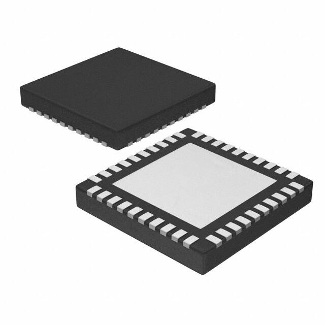


 工商网监
湘ICP备2023018690号
工商网监
湘ICP备2023018690号
