LMX2694-EP
SNAS785C – NOVEMBER 2019 – REVISED OCTOBER 2021
LMX2694-EP 15-GHz Wideband PLLatinum™ RF Synthesizer With Phase
Synchronization
1 Features
3 Description
•
•
•
The LMX2694-EP device is a high-performance,
wideband phase-locked loop (PLL) with an integrated
voltage-controlled oscillator (VCO) and voltage
regulators that can output any frequency between
39.3 MHz and 15.1 GHz without a doubler, eliminating
the need for ½ harmonic filters. The VCO on this
device covers an entire octave to complete the
frequency coverage down to 39.3 MHz. The highperformance PLL, with a –236-dBc/Hz figure of merit
and high-phase detector frequency, can achieve very
low in-band noise and integrated jitter.
•
•
•
•
•
•
•
VID V62/19616
39.3-MHz to 15.1-GHz output frequency
–110 dBc/Hz phase noise at 100-kHz offset with
15-GHz carrier
54-fs RMS jitter at 8 GHz (100 Hz to 100 MHz)
Programmable output power
PLL key specifications
– Figure of merit: –236 dBc/Hz
– Normalized 1/f noise: –129 dBc/Hz
– Up to 200-MHz phase detector frequency
Synchronization of output phase across multiple
devices
Support for SYSREF with 9-ps resolution
programmable delay
3.3-V single power supply operation
Operating temperature range: –55°C to 125°C
The LMX2694-EP allows designers to synchronize
the output of multiple instances of the device. This
means that deterministic phase can be obtained
from a device in any use case, including one with
the fractional engine or output divider enabled. The
device also allows designers to generate or repeat
SYSREF (compliant to JESD204B standard) to use
the device as a low-noise clock source for high-speed
data converters.
2 Applications
•
•
•
•
•
•
•
•
Defense radio
Electronic warfare
Radar
Active antenna system mMIMO (AAS)
Macro remote radio unit
Outdoor backhaul unit
Data acquisition
Wireless communications test equipment
Device Information(1)
PART NUMBER
LMX2694-EP
V62/19616-02XE
(1)
PACKAGE
BODY SIZE (NOM)
VQFN (48)
7.00 mm × 7.00 mm
For all available packages, see the orderable addendum at
the end of the data sheet.
External loop
filter
CPOUT
OSCIN_P
Input
signal
OSCIN
Buffer
VTUNE
RFOUTA_P
Phase
Detector
OSCIN
Doubler
OSCIN_N
Pre-R
Divider
Post-R
Divider
I
MUX
Charge
Pump
Vcc
RFOUTA_N
Channel
Divider
RFOUTB_P
MUX
Sigma-Delta
Modulator
CS#
SCK
SDI
MUXOUT
Serial Interface
Control
N Divider
Vcc
RFOUTB_N
SYSREF
Synchronization
and Delay
Output
Buffers
Simplified Schematic
An IMPORTANT NOTICE at the end of this data sheet addresses availability, warranty, changes, use in safety-critical applications,
intellectual property matters and other important disclaimers. PRODUCTION DATA.
�LMX2694-EP
www.ti.com
SNAS785C – NOVEMBER 2019 – REVISED OCTOBER 2021
Table of Contents
1 Features............................................................................1
2 Applications..................................................................... 1
3 Description.......................................................................1
4 Revision History.............................................................. 2
5 Pin Configuration and Functions...................................3
6 Specifications.................................................................. 5
6.1 Absolute Maximum Ratings........................................ 5
6.2 ESD Ratings............................................................... 5
6.3 Recommended Operating Conditions.........................5
6.4 Thermal Information....................................................5
6.5 Electrical Characteristics.............................................6
6.6 Timing Requirements.................................................. 8
6.7 Timing Diagrams......................................................... 8
6.8 Typical Characteristics.............................................. 10
7 Detailed Description......................................................13
7.1 Overview................................................................... 13
7.2 Functional Block Diagram......................................... 14
7.3 Feature Description...................................................14
7.4 Device Functional Modes..........................................26
7.5 Programming............................................................ 26
7.6 Register Maps...........................................................27
8 Application and Implementation.................................. 72
8.1 Application Information............................................. 72
8.2 Typical Application.................................................... 76
9 Power Supply Recommendations................................78
10 Layout...........................................................................79
10.1 Layout Guidelines................................................... 79
10.2 Layout Example...................................................... 79
11 Device and Documentation Support..........................80
11.1 Device Support........................................................80
11.2 Documentation Support.......................................... 80
11.3 Receiving Notification of Documentation Updates.. 80
11.4 Support Resources................................................. 80
11.5 Trademarks............................................................. 80
11.6 Electrostatic Discharge Caution.............................. 80
11.7 Glossary.................................................................. 80
12 Mechanical, Packaging, and Orderable
Information.................................................................... 80
4 Revision History
NOTE: Page numbers for previous revisions may differ from page numbers in the current version.
Changes from Revision B (May 2020) to Revision C (October 2021)
Page
• Removed equivalent division value of 72 in Table 7-8 .....................................................................................18
• Changed the JESD_DACx values in Table 7-15 ..............................................................................................23
• Changed the R1 register bit name 3 in Figure 7-11 from: 1 to: MUXOUT_CTRL.............................................37
• Changed the OUTA_MUX register description in Table 7-65 .......................................................................... 51
• Changed the OUTB_MUX register description in Table 7-66 .......................................................................... 52
Changes from Revision A (December 2019) to Revision B (May 2020)
Page
• Changed maximum operating temperature to 125°C......................................................................................... 1
• Changed maximum TC to 125°C in Recommended Operating Conditions........................................................ 5
• Changed maximum TC to 125°C in Electrical Characteristics............................................................................ 6
• Changed maximum TC to 125°C in Timing Requirements..................................................................................8
Changes from Revision * (November 2019) to Revision A (December 2019)
Page
• Changed custom data sheet release to catalog ................................................................................................ 1
2
Submit Document Feedback
Copyright © 2021 Texas Instruments Incorporated
Product Folder Links: LMX2694-EP
�LMX2694-EP
www.ti.com
SNAS785C – NOVEMBER 2019 – REVISED OCTOBER 2021
GND
NC
NC
NC
40
39
38
37
GND
BIASVARAC
43
41
VTUNE
44
42
VCCVCO
REFVCO
45
GND
REGVCO
46
GND
48
47
5 Pin Configuration and Functions
CE
1
36
REFVCO2
GND
2
35
SYSREFREQ
BIASVCO
3
34
BIASVCO2
GND
4
33
VCCVCO2
SYNC
5
32
GND
GND
6
31
NC
VCCDIG
7
30
NC
OSCIN_P
8
29
GND
OSCIN_N
9
28
CS#
REGIN
10
27
GND
NC
11
26
RFOUTA_P
NC
12
25
RFOUTA_N
16
17
18
19
20
21
22
23
24
SCK
SDI
NC
RFOUTB_N
RFOUTB_P
MUXOUT
VCCBUF
15
GND
GND
14
CPOUT
VCCMASH
13
VCCCP
Thermal
Pad
Not to scale
Figure 5-1. RTC Package 48-Pin VQFN Top View
Table 5-1. Pin Functions
PIN
NAME
BIASVARAC
NO.
I/O
DESCRIPTION
41
BP
VCO varactor bias. Connect a 10-µF decoupling capacitor to ground.
BIASVCO
3
BP
VCO bias. Connect a 10-µF decoupling capacitor to ground. Place close to pin.
BIASVCO2
34
BP
VCO bias. Connect a 1-µF decoupling capacitor to ground. Place close to pin.
CE
1
I
Chip Enable. High impedance CMOS input. 1.8-V to 3.3-V logic. Active HIGH powers on
the device.
CPOUT
14
O
Charge pump output. Recommend connecting C1 of loop filter close to this pin.
CS#
28
I
SPI latch. High impedance CMOS input. 1.8-V to 3.3-V logic.
GND
2, 4, 32, 40, 42, 47
G
VCO ground.
GND
6, 16, 48
G
Digital ground.
GND
15
G
Charge pump ground.
GND
27, 29
G
Buffer ground.
Multiplexed output. Can output: lock detect, SPI readback and diagnostics.
MUXOUT
23
O
11, 12, 20, 30, 31, 37,
38, 39
NC
OSCIN_N
9
I
Reference input clock (–). High impedance self-biasing pin. Requires AC-coupling
capacitor. (0.1 µF recommended)
OSCIN_P
8
I
Reference input clock (+). High impedance self-biasing pin. Requires AC-coupling
capacitor. (0.1 µF recommended)
REFVCO
44
BP
VCO supply reference. Connect a 10-µF decoupling capacitor to ground.
REFVCO2
36
BP
VCO supply reference. Connect a 10-µF decoupling capacitor to ground.
REGIN
10
BP
Input reference path regulator decoupling. Connect a 1-µF decoupling capacitor to
ground. Place close to pin.
REGVCO
46
BP
VCO regulator node. Connect a 1-µF decoupling capacitor to ground.
RFOUTA_N
25
O
Differential output A (–). Requires connecting 50-Ω resistor pullup to VCC as close as
possible to pin.
NC
Pins may be grounded or left unconnected.
Submit Document Feedback
Copyright © 2021 Texas Instruments Incorporated
Product Folder Links: LMX2694-EP
3
�LMX2694-EP
www.ti.com
SNAS785C – NOVEMBER 2019 – REVISED OCTOBER 2021
Table 5-1. Pin Functions (continued)
PIN
NAME
4
NO.
I/O
DESCRIPTION
RFOUTA_P
26
O
Differential output A (+). Requires connecting 50-Ω resistor pullup to VCC as close as
possible to pin.
RFOUTB_N
21
O
Differential output B (–). Requires connecting 50-Ω resistor pullup to VCC as close as
possible to pin.
RFOUTB_P
22
O
Differential output B (+). Requires connecting 50-Ω resistor pullup to VCC as close as
possible to pin.
SCK
18
I
SPI clock. High impedance CMOS input. 1.8-V to 3.3-V logic.
SDI
19
I
SPI data. High impedance CMOS input. 1.8-V to 3.3-V logic.
SYNC
5
I
Phase synchronization input. Has programmable threshold. Connect to ground if not
being used.
SYSREFREQ
35
I
SYSREF request input for JESD204B support. Connect to ground if not being used.
VCCBUF
24
P
Output buffer supply. Connect to 3.3-V and a 0.1-µF decoupling capacitor to ground.
VCCCP
13
P
Charge pump supply. Connect to 3.3-V and a 0.1-µF decoupling capacitor to ground.
VCCDIG
7
P
Digital supply. Connect to 3.3-V and a 0.1-µF decoupling capacitor to ground.
VCCMASH
17
P
Digital supply. Connect to 3.3-V and a 1-µF decoupling capacitor to ground.
VCCVCO
45
P
VCO supply. Connect to 3.3-V and a 1-µF decoupling capacitor to ground.
VCCVCO2
33
P
VCO supply. Connect to 3.3-V and a 1-µF decoupling capacitor to ground.
VTUNE
43
I
VCO tuning voltage input. Connect a 1.5-nF or more capacitor to VCO ground. See
External Loop Filter for details.
Thermal pad
—
—
Connect the GND pin to the exposed thermal pad for correct operation. Connect the
thermal pad to any internal PCB ground plane using multiple vias for good thermal
performance.
Submit Document Feedback
Copyright © 2021 Texas Instruments Incorporated
Product Folder Links: LMX2694-EP
�LMX2694-EP
www.ti.com
SNAS785C – NOVEMBER 2019 – REVISED OCTOBER 2021
6 Specifications
6.1 Absolute Maximum Ratings
over operating free-air temperature range (unless otherwise noted)(1)
MIN
MAX
–0.3
3.6
UNIT
VCC
Power supply voltage
VIN
IO input voltage
VCC + 0.3
V
TJ
Junction temperature
–55
150
°C
Tstg
Storage temperature
–65
150
°C
(1)
V
Stresses beyond those listed under Absolute Maximum Rating may cause permanent damage to the device. These are stress
ratings only, which do not imply functional operation of the device at these or any other conditions beyond those indicated
under Recommended Operating Condition. Exposure to absolute-maximum-rated conditions for extended periods may affect device
reliability.
6.2 ESD Ratings
VALUE
V(ESD)
(1)
(2)
Electrostatic discharge
Human-body model (HBM), per ANSI/ESDA/JEDEC
JS-001(1)
±1000
Charged device model (CDM), per JEDEC
specification JESD22-C101, all pins(2)
±1000
UNIT
V
JEDEC document JEP155 states that 500 V HBM allows safe manufacturing with a standard ESD control process.
JEDEC document JEP157 states that 250 V CDM allows safe manufacturing with a standard ESD control process.
6.3 Recommended Operating Conditions
over operating free-air temperature range (unless otherwise noted)
MIN
TC
Case temperature
–55
VCC
Supply input voltage
3.2
NOM
3.3
MAX
UNIT
125
°C
3.45
V
6.4 Thermal Information
LMX2694-EP
THERMAL
METRIC(1)
RTC (VQFN)
UNIT
48 PINS
RθJA
Junction-to-ambient thermal resistance
22.4
°C/W
RθJC(top)
Junction-to-case (top) thermal resistance
10.0
°C/W
RθJB
Junction-to-board thermal resistance
6.1
°C/W
ΨJT
Junction-to-top characterization parameter
0.1
°C/W
ΨJB
Junction-to-board characterization parameter
6.0
°C/W
RθJC(bot)
Junction-to-case (bottom) thermal resistance
0.7
°C/W
(1)
For more information about traditional and new thermal metrics, see the Semiconductor and IC Package Thermal Metrics application
report.
Submit Document Feedback
Copyright © 2021 Texas Instruments Incorporated
Product Folder Links: LMX2694-EP
5
�LMX2694-EP
www.ti.com
SNAS785C – NOVEMBER 2019 – REVISED OCTOBER 2021
6.5 Electrical Characteristics
3.2 V ≤ VCC ≤ 3.45 V, –50°C ≤ TC ≤ 125°C. Typical values are at VCC = 3.3 V, 25°C (unless otherwise noted)
PARAMETER
TEST CONDITIONS
MIN
TYP
MAX
UNIT
POWER SUPPLY
OUTA_PD = 0; OUTB_PD = 1;
OUTA_MUX = OUTB_MUX = 1;
OUTA_PWR = 31; CPG = 7;
fOSC = fPD = 100 MHz; fVCO = fOUT = 14.5 GHz
360
Power on reset current
RESET = 1
289
Power down current
POWERDOWN = 1
Supply current
ICC
mA
6
OUTPUT CHARACTERISTICS
Single-ended output power(1)
pOUT
(2)
50-Ω resistor pull-up
OUTx_PWR = 31
fOUT = 8 GHz
2
fOUT = 15 GHz
0
dBm
INPUT SIGNAL PATH
fOSC
Reference input frequency
VOSC
Reference input voltage(3)
OSC_2X = 0
5
1000
OSC_2X = 1
5
200
fOSC ≥ 20 MHz
0.4
2
10 MHz ≤ fOSC < 20 MHz
0.8
2
5 MHz ≤ fOSC < 10 MHz
1.6
2
MASH_ORDER = 0
0.125
250
MASH_ORDER > 0
5
200
MHz
VPP
PHASE DETECTOR AND CHARGE PUMP
Phase detector frequency(4)
fPD
ICPOUT
Charge-pump leakage current
CPG = 0
Effective charge pump current
Sum of the up and down currents
PNPLL_1/f
Normalized PLL 1/f noise
PNPLL_FOM
Normalized PLL noise floor
20
3
nA
15
–129
fPD = 100 MHz; fVCO = 12 GHz(5)
MHz
mA
dBc/Hz
–236
VCO CHARACTERISTICS
fVCO
6
VCO frequency
7550
Submit Document Feedback
15100
MHz
Copyright © 2021 Texas Instruments Incorporated
Product Folder Links: LMX2694-EP
�LMX2694-EP
www.ti.com
SNAS785C – NOVEMBER 2019 – REVISED OCTOBER 2021
3.2 V ≤ VCC ≤ 3.45 V, –50°C ≤ TC ≤ 125°C. Typical values are at VCC = 3.3 V, 25°C (unless otherwise noted)
PARAMETER
TEST CONDITIONS
MIN
100 kHz
VCO1
fVCO = 8.1 GHz
1 MHz
–154
–105
1 MHz
–126.5
10 MHz
–146.5
100 MHz
PNVCO
VCO phase noise
VCO4
fVCO = 11.4 GHz
VCO5
fVCO = 12.5 GHz
VCO6
fVCO = 13.6 GHz
–154
100 kHz
–103.5
1 MHz
–125.5
10 MHz
–146
100 MHz
–158
100 kHz
–102.5
1 MHz
–124.5
10 MHz
–145
100 MHz
–160
100 kHz
–100.5
1 MHz
–122.5
10 MHz
–143.5
100 MHz
–154.5
100 kHz
–99.5
1 MHz
–122
10 MHz
–154
100 kHz
–98
1 MHz
–120.5
10 MHz
–141.5
100 MHz
tVCOCAL
KVCO
VCO calibration time(6)
VCO Gain
dBc/Hz
–142.5
100 MHz
VCO7
fVCO = 14.7 GHz
UNIT
–147.5
100 kHz
VCO3
fVCO = 10.4 GHz
MAX
–128
10 MHz
100 MHz
VCO2
fVCO = 9.3 GHz
TYP
–106.5
–155
Switch across the entire frequency band;
fOSC = fPD = 100 MHz;
VCO_SEL = 7
650
8.1 GHz
94
9.3 GHz
106
10.4 GHz
122
11.4 GHz
148
12.5 GHz
185
13.6 GHz
202
14.7 GHz
233
|ΔTCL|
Allowable temperature drift
VCO not being re-calibrated
125
H2
VCO second harmonic
fVCO = 8 GHz; divider disabled
–30
H3
VCO third harmonic
fVCO = 8 GHz; divider disabled
–25
µs
MHz/V
°C
dBc
DIGITAL INTERFACE
VIH
High-level input voltage
1.4
V
VIL
Low-level input voltage
0.4
V
IIH
High-level input current
–100
100
µA
IIL
Low-level input current
–100
100
µA
Submit Document Feedback
Copyright © 2021 Texas Instruments Incorporated
Product Folder Links: LMX2694-EP
7
�LMX2694-EP
www.ti.com
SNAS785C – NOVEMBER 2019 – REVISED OCTOBER 2021
3.2 V ≤ VCC ≤ 3.45 V, –50°C ≤ TC ≤ 125°C. Typical values are at VCC = 3.3 V, 25°C (unless otherwise noted)
PARAMETER
TEST CONDITIONS
VOH
High-level output voltage
Load current = –5 mA
VOL
High-level output current
Load current = 5 mA
(1)
(2)
(3)
(4)
(5)
(6)
MUXOUT pin
MIN
TYP
MAX
VCC – 0.6
UNIT
V
0.6
V
Single ended output power obtained after de-embedding microstrip trace losses and matching with a manual tuner. Unused port
terminated to 50-Ω load.
Output power, spurs, and harmonics can vary based on board layout and components.
Single-ended AC coupled sine wave input with complementary side AC coupled to ground with 50-Ω resistor.
For lower VCO frequencies, the N divider minimum value can limit the phase-detector frequency.
The PLL noise contribution is measured using a clean reference and a wide loop bandwidth and is composed into flicker and flat
components. PLL_flat = PLL_FOM + 20 x log(fVCO/fPD) + 10 x log(fPD/1 Hz). PLL_flicker (offset) = PLL_1/f + 20 x log(fVCO/1 GHz) - 10
x log(offset/10 kHz). Once these two components are found, the total PLL noise can be calculated as PLL_Noise = 10 x log(10PLL_Flat/
10 + 10PLL_flicker/10).
See Section 7.3.7.1 for details.
6.6 Timing Requirements
3.2 V ≤ VCC ≤ 3.45 V, –50°C ≤ TC ≤ 125°C. Typical values are at VCC = 3.3 V, 25°C (unless otherwise noted)
MIN
NOM
MAX
UNIT
SYNC AND SYSREFREQ TIMING
tSETUP
Setup time for pin relative to OSCIN rising edge
tHOLD
Hold time for pin relative to OSCIN rising edge
See Figure 6-1
9
ns
4
ns
DIGITAL INTERFACE WRITE SPECIFICATIONS
fSPIWrite
SPI write speed
tCE
Clock to enable low time
tCWL + tCWH ≥ 25 ns
5
ns
tCS
Data to clock setup time
2
ns
tCH
Data to clock hold time
2
ns
tCWH
Clock pulse width high
5
ns
tCWL
Clock pulse width low
5
ns
tCES
Enable to clock setup time
5
ns
tEWH
Enable pulse width high
2
ns
See Figure 6-2
40
MHz
DIGITAL INTERFACE READBACK SPECIFICATIONS
fSPIReadback SPI readback speed
40
MHz
tCE
Clock to enable low time
5
ns
tCS
Clock to data wait time
2
ns
tCH
Clock to data hold time
tCWH
Clock pulse width high
tCWL
Clock pulse width low
tCES
Enable to clock setup time
tEWH
Enable pulse width high
2
tCD
Falling clock edge to data wait time
See Figure 6-3
2
ns
10
ns
10
ns
5
ns
ns
8
ns
6.7 Timing Diagrams
SYNC
or
SYSREFREQ
tSETUP
tHOLD
OSCIN
Figure 6-1. Trigger Signals Timing Diagram
8
Submit Document Feedback
Copyright © 2021 Texas Instruments Incorporated
Product Folder Links: LMX2694-EP
�LMX2694-EP
www.ti.com
SNAS785C – NOVEMBER 2019 – REVISED OCTOBER 2021
MSB
SDI
LSB
R/W
A5
A0
D15
D14
D0
SCK
tCS
tCES
tCWH
tCH
tCE
tCWL
CS#
tEWH
Figure 6-2. Serial Data Input Timing Diagram
There are several other considerations for writing on the SPI:
• The R/W bit must be set to 0.
• The data on SDI pin is clocked into a shift register on each rising edge on the SCK pin.
• The CS# must be held low for data to be clocked. Device will ignore clock pulses if CS# is held high.
• The CS# transition from high to low must occur when SCK is low.
• When SCK and SDI lines are shared between devices, TI recommends to hold the CS# line high on the
device that is not to be clocked.
LSB
MUXOUT
RB15
R/W
RB0
tCD
MSB
SDI
RB14
A6
A5
A0
SCK
tCE
tCWH
tCES
tCWL
tCS
CS#
tEWH
Figure 6-3. Serial Data Readback Timing Diagram
There are several other considerations for SPI readback:
• The R/W bit must be set to 1.
• The MUXOUT pin will always be low for the address portion of the transaction.
• The data on MUXOUT becomes available momentarily after the falling edge of SCK, and therefore, should be
read back on the rising edge of SCK.
• The data portion of the transition on the SDI line is always ignored.
Submit Document Feedback
Copyright © 2021 Texas Instruments Incorporated
Product Folder Links: LMX2694-EP
9
�LMX2694-EP
www.ti.com
SNAS785C – NOVEMBER 2019 – REVISED OCTOBER 2021
6.8 Typical Characteristics
-60
-60
-70
-70
-80
-80
Phase noise (dBc/Hz)
Phase noise (dBc/Hz)
At TA = 25°C, unless otherwise noted
-90
-100
-110
-120
-130
-140
-120
-130
-140
-150
9.3 GHz
-160
100
1k
10k
100k
1M
10M
100M
fOSC = 100 MHz
fPD = 200 MHz
-70
-70
-80
-80
Phase noise (dBc/Hz)
-60
-90
-100
-110
-120
-130
-140
-120
-130
-140
11.4 GHz
-160
100
1k
100M
Offset (Hz)
fOSC = 100 MHz
fPD = 200 MHz
Figure 6-6. Closed Loop Phase Noise at 10.4 GHz
-70
-80
-80
Phase noise (dBc/Hz)
-70
-90
-100
-110
-120
-130
-140
tc-0
Jitter = 61.7 fs (100 Hz - 100 MHz)
-110
-120
-130
-140
-150
13.6 GHz
-160
100
1k
100M
Offset (Hz)
Jitter = 68.8 fs (100 Hz - 100 MHz)
10k
100k
1M
10M
100M
Offset (Hz)
tc-0
Figure 6-8. Closed Loop Phase Noise at 12.5 GHz
100M
-90
12.5 GHz
-160
100
1k
fOSC = 100 MHz
fPD = 200 MHz
10M
-100
-150
10M
1M
Figure 6-7. Closed Loop Phase Noise at 11.4 GHz
-60
1M
100k
Offset (Hz)
-60
100k
10k
tc-0
Jitter = 61.8 fs (100 Hz - 100 MHz)
10k
tc-0
Jitter = 61.8 fs (100 Hz - 100 MHz)
-110
-150
fOSC = 100 MHz
fPD = 200 MHz
100M
-100
10.4 GHz
-160
100
1k
10M
10M
-90
-150
1M
1M
Figure 6-5. Closed Loop Phase Noise at 9.3 GHz
-60
100k
100k
Offset (Hz)
Jitter = 61.2 fs (100 Hz - 100 MHz)
10k
10k
tc-0
Figure 6-4. Closed Loop Phase Noise at 8.1 GHz
Phase noise (dBc/Hz)
-110
8.1 GHz
-160
100
1k
fOSC = 100 MHz
fPD = 200 MHz
Phase noise (dBc/Hz)
-100
-150
Offset (Hz)
10
-90
fOSC = 100 MHz
fPD = 200 MHz
tc-0
Jitter = 67.8 fs (100 Hz - 100 MHz)
Figure 6-9. Closed Loop Phase Noise at 13.6 GHz
Submit Document Feedback
Copyright © 2021 Texas Instruments Incorporated
Product Folder Links: LMX2694-EP
�LMX2694-EP
www.ti.com
SNAS785C – NOVEMBER 2019 – REVISED OCTOBER 2021
6.8 Typical Characteristics (continued)
At TA = 25°C, unless otherwise noted
-60
-90
-70
Phase noise (dBc/Hz)
-80
Phase noise (dBc/Hz)
Measurement
Flicker noise
Flat noise
Modeled phase noise
-95
-90
-100
-110
-120
-130
-140
-100
-105
-110
-115
-120
-125
-150
14.7 GHz
-160
100
1k
10k
100k
1M
10M
Offset (Hz)
fOSC = 100 MHz
fPD = 200 MHz
-130
100
100M
fPD = 200 MHz
fVCO = 10 GHz
Jitter = 67.8 fs (100 Hz - 100 MHz)
100k
1M
tc-0
FOM = –237.5 dBc/Hz
Flicker = –130.5 dBc/Hz
Figure 6-11. Calculation of PLL Noise Metrics
Figure 6-10. Closed Loop Phase Noise at 14.7 GHz
4
Flicker noise
FOM
8
3
Change in phase noise (dB)
Degradation in PLL noise metric (dB)
10k
Offset (Hz)
9
7
6
5
4
3
2
1
0
-1
100
1k
tc-0
200
300
400
500
Slew rate (V/Ps)
600
700
800
2
1
0
-1
-2
-3
-4
-5
-6
10k
fVCO = 10 GHz
LBW < 100 Hz
Figure 6-12. PLL Phase Noise Metrics vs fosc Slew Rate
100k
1M
Offset (Hz)
tc-0
fOSC = 200 MHz
fVCO = 14.8 GHz
TA =
55qC
25qC
85qC
125qC
10M
100M
tc-1
VCO re-calibrated at final temperature
Figure 6-13. Change in VCO Phase Noise Over Temperature
Submit Document Feedback
Copyright © 2021 Texas Instruments Incorporated
Product Folder Links: LMX2694-EP
11
�LMX2694-EP
www.ti.com
SNAS785C – NOVEMBER 2019 – REVISED OCTOBER 2021
6.8 Typical Characteristics (continued)
4
-80
3
-90
2
-100
Phase noise (dBc/Hz)
Change in phase noise (dB)
At TA = 25°C, unless otherwise noted
1
0
-1
-2
-3
-4
TA = 55qC, TLock = 25qC
TA = 55qC, TLock = 55qC
TA = 125qC, TLock = 25qC
TA = 125qC, TLock = 125qC
-5
-6
-7
10k
100k
1M
Offset (Hz)
fVCO = 10 GHz
LBW < 100 Hz
10M
-110
-120
-130
-140
-150
-160
-170
-180
1k
100M
tc-1
VCO calibrated at 25°C and temperature
drifted
Figure 6-14. Change in VCO Phase Noise Over Temperature
12
8 GHz
4 GHz
2 GHz
1 GHz
500 MHz
250 MHz
125 MHz
62.5 MHz
10k
100k
1M
10M
Offset (Hz)
100M
tc-1
.
.
.
Figure 6-15. Divided Output Frequency
Submit Document Feedback
Copyright © 2021 Texas Instruments Incorporated
Product Folder Links: LMX2694-EP
�LMX2694-EP
www.ti.com
SNAS785C – NOVEMBER 2019 – REVISED OCTOBER 2021
7 Detailed Description
7.1 Overview
The LMX2694-EP is a high-performance, wideband frequency synthesizer with an integrated VCO and output
divider. The VCO operates from 7550 to 15100 MHz, and can be combined with the output divider to produce
any frequency in the range of 39.3 MHz to 15.1 GHz. There are two dividers within the input path.
The PLL is fractional-N PLL with a programmable delta-sigma modulator up to the 3rd order. The fractional
denominator is a programmable 32-bit long that can provide fine frequency steps easily below 1-Hz resolution,
as well as be used to do exact fractions like 1/3, 7/1000, and so on.
For applications where deterministic or adjustable phase is desired, the SYNC pin can be used to get the phase
relationship between the OSCIN and RFOUTx pins deterministic. Once this is done, the phase can be adjusted
in very fine steps of the VCO period divided by the fractional denominator.
The ultra-fast VCO calibration is designed for applications where the frequency must be swept or abruptly
changed. The frequency can be manually programmed.
For JESD204B support, the RFOUTB output can be used as a differential SYSREF output that can be either
a single pulse or a series of pulses that occur at a programmable distance away from the rising edges of the
output signal.
The LMX2694-EP device requires only a single 3.3-V power supply. The internal power supplies are provided by
integrated LDOs, eliminating the need for high-performance external LDOs.
Table 7-1 shows the range of several of the doubler, dividers, and fractional settings.
Table 7-1. Range of Doubler, Divider, and Fractional Settings
PARAMETER
MIN
MAX
COMMENTS
OSCIN doubler
0 (1X)
1 (2X)
The low noise doubler can be used to increase the
phase detector frequency to improve phase noise and
avoid spurs. This is in reference to the OSC_2X bit.
Pre-R divider
1 (bypass)
128
Only use the Pre-R divider if the input frequency is too
high for the Post-R divider.
Post-R divider
1 (bypass)
255
The maximum input frequency for the Post-R divider is
250 MHz. Use the Pre-R divider if necessary.
N divider
≥ 28
524287
The minimum divide depends on modulator order and
VCO frequency. See N Divider and Fractional Circuitry
for more details.
Fractional numerator /
denominator
1 (integer mode)
232 – 1 = 4294967295
The fractional denominator is programmable and can
assume any value between 1 and 232– 1. It is not a
fixed denominator.
Fractional order
0
3
Channel divider
1 (bypass)
192
Output frequency
39.3 MHz
15.1 GHz
Order 0 is integer mode, and the order can be
programmed.
This is the series of several dividers. Also, be aware
that above 10 GHz, the maximum allowable channel
divider value is 6.
This is implied by the minimum VCO frequency divided
by the maximum channel divider value.
Submit Document Feedback
Copyright © 2021 Texas Instruments Incorporated
Product Folder Links: LMX2694-EP
13
�LMX2694-EP
www.ti.com
SNAS785C – NOVEMBER 2019 – REVISED OCTOBER 2021
7.2 Functional Block Diagram
CPOUT
OSCIN_P
OSCIN
Buffer
Input
signal
VTUNE
RFOUTA_P
Phase
Detector
OSCIN
Doubler
Pre-R
Divider
Post-R
Divider
I
OSCIN_N
MUX
Charge
Pump
Vcc
RFOUTA_N
Channel
Divider
RFOUTB_P
MUX
Sigma-Delta
Modulator
CS#
SCK
SDI
Serial Interface
Control
RFOUTB_N
SYSREF
Synchronization
and Delay
N Divider
MUXOUT
Vcc
Output
Buffers
7.3 Feature Description
7.3.1 Reference Oscillator Input
The OSCIN pins are used as a frequency reference input to the device. The input is high impedance and
requires AC-coupling caps at the pin. The OSCIN pins can be driven single-ended with a CMOS clock or
XO. Differential clock input is also supported, making it easier to interface with high-performance system clock
devices such as TI’s LMK series clock devices. As the OSCIN signal is used as a clock for the VCO calibration,
a proper reference signal must be applied at the OSCIN pin at the time of programming FCAL_EN.
7.3.2 Reference Path
The reference path consists of an OSCIN doubler (OSC_2X), Pre-R divider, and a Post-R divider.
OSCIN_P
Input
signal
OSCIN
Buffer
OSCIN
Doubler
Pre-R
Divider
Post-R
Divider
OSCIN_N
Figure 7-1. Reference Path Diagram
The OSCIN doubler (OSC_2X) can double up low OSCIN frequencies. Pre-R (PLL_R_PRE) and Post-R
(PLL_R) dividers both divide frequency down. Use Equation 1 to calculate the phase detector frequency, fPD:
fPD = fOSC × OSC_2X / (PLL_R_PRE × PLL_R)
•
•
(1)
If the OSCIN doubler is used, the OSCIN signal should have a 50% duty cycle as both the rising and falling
edges are used.
If the OSCIN doubler is not used, only rising edges of the OSCIN signal are used and duty cycle is not
critical.
7.3.2.1 OSCIN Doubler (OSC_2X)
The OSCIN doubler allows the user to double the input reference frequency at up to 400 MHz, while adding
minimal noise. It may be advantageous to use the doubler to go higher than the maximum phase detector
frequency in some situations, because the Pre-R divider may be able to divide down this frequency to a phase
detector frequency that is advantageous for fractional spurs.
7.3.2.2 Pre-R Divider (PLL_R_PRE)
The Pre-R divider is useful for reducing the input frequency to help meet the maximum 250-MHz input frequency
limitation to the PLL-R divider. Otherwise, it does not have to be used.
7.3.2.3 Post-R Divider (PLL_R)
The Post-R divider can be used to further divide down the frequency to the phase detector frequency. When
PLL_R > 1, the input frequency to this divider is limited to 250 MHz.
14
Submit Document Feedback
Copyright © 2021 Texas Instruments Incorporated
Product Folder Links: LMX2694-EP
�LMX2694-EP
www.ti.com
SNAS785C – NOVEMBER 2019 – REVISED OCTOBER 2021
7.3.3 State Machine Clock
The state machine clock is a divided-down version of the OSCIN signal that is used internally in the device.
This divide value 1, 2, 4, 8, 16, or 32 and is determined by CAL_CLK_DIV programming word (described in the
Programming section). This state machine clock impacts various features like the VCO calibration. The state
machine clock is calculated as fSM = fOSC / 2CAL_CLK_DIV.
7.3.4 PLL Phase Detector and Charge Pump
The phase detector compares the outputs of the Post-R divider and N divider, and will generate a correction
current corresponding to the phase error until the two signals are aligned in-phase. This charge-pump current is
software-programmable to many different levels, which allows the user to modify the closed-loop bandwidth of
the PLL.
7.3.5 N Divider and Fractional Circuitry
The N divider includes fractional compensation that can achieve any fractional denominator from 1 to (232 – 1).
The integer portion of N is the whole part of the N divider value, while the fractional portion (Nfrac = NUM / DEN)
is the remaining fraction. In general, the total N divider value is determined by N + NUM / DEN. The N, NUM and
DEN are software-programmable. The higher the denominator, the finer the resolution step of the output. For
example, even when using fPD = 200 MHz, the output can increment in steps of 200 MHz / ( 232 – 1) = 0.047 Hz.
Equation 2 shows the relationship between the phase detector and VCO frequencies. Note that in SYNC mode,
there is an extra divider that is not shown in Equation 2.
fVCO = fPD × [N + NUM/DEN]
(2)
The sigma-delta modulator that controls this fractional division is also programmable from integer mode to the
third order. To make the fractional spurs consistent, the modulator is reset any time that the R0 register is
programmed.
The N divider has minimum value restrictions based on the modulator order (MASH_ORDER) and VCO
frequency. Furthermore, the PFD_DLY_SEL bit must be programmed in accordance to Table 7-2. IncludedDivide
may be larger than one in SYNC mode. In all other modes, IncludedDivide is just one.
Table 7-2. Minimum N Divider Restrictions
MASH_ORDER
fVCO / IncludedDivide (MHz)
MINIMUM N
PFD_DLY_SEL
0
1
2
3
≤ 12500
29
1
> 12500
33
2
≤ 10000
30
1
10000 - 12500
34
2
> 12500
38
3
≤ 4000 (SYNC mode)
31
1
4000 - 7500 (SYNC mode)
31
2
7500 - 10000
32
2
> 10000
36
3
≤ 4000 (SYNC mode)
33
1
4000 - 7500 (SYNC mode)
37
2
7500 - 10000
41
3
> 10000
45
4
7.3.6 MUXOUT Pin
The MUXOUT pin can be configured as either a lock detect indicator for the PLL or as a serial data output for the
SPI interface to read back registers. Field MUXOUT_LD_SEL (register R0[2]) configures this output.
Submit Document Feedback
Copyright © 2021 Texas Instruments Incorporated
Product Folder Links: LMX2694-EP
15
�LMX2694-EP
www.ti.com
SNAS785C – NOVEMBER 2019 – REVISED OCTOBER 2021
Table 7-3. MUXOUT Pin Configurations
MUXOUT_LD_SEL
FUNCTION
0
Serial data output for readback
1
Lock detect indicator
When the lock detect indicator is selected, there are two types of indicators that can be selected with the field
LD_TYPE (register R59[0]). The first indicator is called “VCOCal” (LD_TYPE = 0), and the second indicator is
called “Vtune and VCOCal” (LD_TYPE = 1).
7.3.6.1 Serial Data Output for Readback
In this mode, the MUXOUT pin can be used as a the serial data output of the SPI interface. This output cannot
be in a tri-state condition, therefore no line sharing is possible. Details of this pin operation are described in
Timing Requirements. Readback is very useful when a device is used in full-assist mode, because the VCO
calibration data are retrieved and saved for future use. It can also be used to read back the lock detect status
using the field rb_LD_VTUNE(register R110[10:9]).
7.3.6.2 Lock Detect Indicator Set as Type “VCOCal”
In this mode, the MUXOUT pin will be low when the VCO is calibrating or when the lock detect delay timer is
running. Otherwise, the MUXOUT will be high. The programmable timer (LD_DLY, register R60[15:0]) adds an
additional delay after the VCO calibration finishes and before the lock detect indicator is asserted high. LD_DLY
is a 16-bit unsigned quantity that corresponds to the 4 times the number of phase detector cycles in absolute
delay. For example, a phase detector frequency of 100 MHz and the LD_DLY = 10000 will add a delay of 400
µs before the indicator is asserted. This indicator will remain in its current state (high or low) until register R0 is
programmed with FCAL_EN = 1 with a valid input reference. In other words, if the PLL goes out of lock or the
input reference goes away when the current state is high, then the current state will remain high.
7.3.6.3 Lock Detect Indicator Set as Type “Vtune and VCOCal”
In this mode the MUXOUT pin will be high when the VCO calibration has finished, the lock detect delay timer is
finished running, and the PLL is locked. This indicator may remain in its current state (high or low) if the OSCin
signal is lost. The true status of the indicator will be updated and resume its operation only when a valid input
reference to the OSCin pin is returned. An alternative method to monitor the OSCin of the PLL is recommended.
This indicator is reliable as long as the reference to OSCin is present.
The output of the device can be automatically muted when lock detect indicator “Vtune and VCOCal” is low. This
feature is enabled with the field OUT_MUTE (register R0[9]) asserted.
7.3.7 VCO (Voltage-Controlled Oscillator)
The LMX2694-EP includes a fully integrated VCO. The VCO takes the voltage from the loop filter and converts
this into a frequency. The VCO frequency is related to the other frequencies and as follows:
fVCO = fPD × N divider × IncludedDivide
(3)
7.3.7.1 VCO Calibration
To reduce the VCO tuning gain, and therefore improve the VCO phase-noise performance, the VCO frequency
range is divided into several different frequency bands. The entire range (7550 to 15100 MHz) covers an octave
that allows the divider to take care of frequencies below the lower bound. This creates the need for frequency
calibration to determine the correct frequency band given a desired output frequency. The frequency calibration
routine is activated any time that the R0 register is programmed with the FCAL_EN = 1. It is important that a
valid OSCIN signal must present before VCO calibration begins.
The VCO also has an internal amplitude calibration algorithm to optimize the phase noise, which is also
activated any time the R0 register is programmed.
The optimum internal settings for this are temperature-dependent. If the temperature is allowed to drift too much
without being recalibrated, some minor phase noise degradation could result. The maximum allowable drift for
16
Submit Document Feedback
Copyright © 2021 Texas Instruments Incorporated
Product Folder Links: LMX2694-EP
�LMX2694-EP
www.ti.com
SNAS785C – NOVEMBER 2019 – REVISED OCTOBER 2021
continuous lock, ΔTCL, is stated in the electrical specifications. For this device, a number of 125°C means the
device never loses lock if the device is operated under recommended operating conditions.
The LMX2694-EP allows the user to assist the VCO calibration. In general, there are three kinds of assistance,
as shown in Table 7-4.
Table 7-4. Assisting the VCO Calibration Speed
ASSISTANCE
LEVEL
DESCRIPTION
VCO_SEL
VCO_SEL_FORCE
VCO_CAPCTRL_FORCE
VCO_DACISET_FORCE
VCO_CAPCTRL
VCO_DACISET
No assist
User does nothing to improve VCO calibration speed.
7
0
Don't care
Partial assist
Upon every frequency change, before the FCAL_EN
bit is checked, the user provides the initial starting
VCO_SEL.
Choose by table
0
Don't care
Full assist
The user forces the VCO core (VCO_SEL), amplitude
settings (VCO_DACISET), and frequency band
(VCO_CAPCTRL) and manually sets the value.
Choose by readback
1
Choose by readback
For the no-assist method, just set VCO_SEL = 7 and this is done. For partial-assist, the VCO calibration speed
can be improved by changing the VCO_SEL bit according to frequency. Note that the frequency is not the actual
VCO core range, but actually favors choosing the VCO. This is not only optimal for VCO calibration speed, but
required for reliable locking.
Table 7-5. Minimum VCO_SEL for Partial Assist
fVCO
VCO CORE (MIN)
7550 - 8740 MHz
VCO1
8740 - 10000 MHz
VCO2
10000 - 10980 MHz
VCO3
10980 - 12100 MHz
VCO4
12100 - 13080 MHz
VCO5
13080 - 14180 MHz
VCO6
14180 - 15100 MHz
VCO7
For fastest calibration time, it is ideal to use the minimum VCO core as recommended in Table 7-5. The Table
7-6 shows typical VCO calibration times (in µs) for this choice in bold as well as showing how long the calibration
time is increased if a higher than necessary VCO core is chosen. Realize that these calibration times are specific
to these fOSC and fPD conditions specified and at the boundary of two cores, sometimes the calibration time can
be increased.
Table 7-6. Typical Calibration Times for fOSC = fPD = 100 MHz Based on VCO_SEL
fVCO (GHz)
VCO_SEL
VCO7
VCO6
VCO5
VCO4
VCO3
VCO2
VCO1
8.1
650
540
550
440
360
230
110
9.3
610
530
540
430
320
220
Invalid
10.4
590
520
530
430
240
11.4
340
290
280
180
12.5
270
170
120
13.6
240
130
14.7
160
Invalid
Invalid
Invalid
Invalid
Invalid
7.3.7.2 Determining the VCO Gain
The VCO gain varies between the seven cores, and is the lowest at the lowest end of the band and highest at
the highest end of each band. For a more accurate estimation, use Table 7-7.
Submit Document Feedback
Copyright © 2021 Texas Instruments Incorporated
Product Folder Links: LMX2694-EP
17
�LMX2694-EP
www.ti.com
SNAS785C – NOVEMBER 2019 – REVISED OCTOBER 2021
Table 7-7. VCO Gain
f1
f2
KVCO1
KVCO2
7550
8740
78
114
8740
10000
91
125
10000
10980
112
136
10980
12100
136
168
12100
13080
171
206
13080
14180
188
218
14180
15100
218
248
Based ion Table 7-7, Equation 4 can estimate the VCO gain for an arbitrary VCO frequency of fVCO:
KVCO = KVCO1 + (KVCO2 – KVCO1) × (fVCO – f1) / (f2 – f1)
(4)
7.3.8 Channel Divider
To go below the VCO lower bound of 7550 MHz, the channel divider can be used. The channel divider consists
of four segments, and the total division value is equal to the multiplication of them. Therefore, not all values are
valid.
VCO
1/2
Divide by
2 or 3
Divide by
2 or 4
Divide by
2, 4, or 8
MUX
RFOUTA
MUX
RFOUTB
MUX
Figure 7-2. Channel Divider
When the channel divider is used, there are limitations on the values. Table 7-8 shows how these values are
implemented and which segments are used.
Table 7-8. Channel Divider Segments
EQUIVALENT
DIVISION VALUE
FREQUENCY
LIMITATION
2
OUTPUT FREQUENCY (MHz)
MIN
MAX
CHDIV[4:0]
SEG0
SEG1
SEG2
SEG3
3775
7550
0
2
1
1
1
1887.5
3775
1
2
2
1
1
6
1258.333
2516.667
2
2
3
1
1
8
943.75
1437.5
3
2
2
2
1
12
629.167
958.333
4
2
3
2
1
16
471.875
718.75
5
2
2
4
1
24
314.583
469.167
6
2
3
4
1
32
235.938
359.375
7
2
2
8
1
4
48
None
fVCO ≤ 11.5 GHz
157.292
239.583
8
2
3
8
1
64
117.969
179.688
9
2
2
8
2
96
78.646
119.792
10
2
3
8
2
128
58.984
89.844
11
2
2
8
4
39.323
59.896
12
2
3
8
4
n/a
n/a
13 - 31
n/a
n/a
n/a
n/a
192
Invalid
n/a
The channel divider is powered up whenever an output (OUTx_MUX) is selected to the channel divider or
SYSREF, regardless of whether it is powered down or not. When an output is not used, TI recommends
selecting the VCO output to ensure that the channel divider is not unnecessarily powered up.
18
Submit Document Feedback
Copyright © 2021 Texas Instruments Incorporated
Product Folder Links: LMX2694-EP
�LMX2694-EP
www.ti.com
SNAS785C – NOVEMBER 2019 – REVISED OCTOBER 2021
Table 7-9. Channel Divider
OUTA MUX
OUTB MUX
CHANNEL DIVIDER
Channel Divider
X
Powered up
X
Channel Divider or SYSREF
Powered up
All other cases
Powered down
7.3.9 Output Buffer
The RF output buffer type is open-collector that requires an external pullup to VCC. This component may be
a 50-Ω resistor or an inductor. The inductor has less controlled impedance, but higher power. For the inductor
case, it is often helpful to follow this with a resistive pad. The output power can be programmed to various levels
or disabled while still keeping the PLL in lock.
Table 7-10. OUTx_PWR Recommendations
fOUT
RESTRICTIONS
COMMENTS
At lower frequencies, the output buffer impedance is high, so the 50-Ω
pullup will make the output impedance look somewhat like 50 Ω.
10 MHz ≤ fOUT ≤ 5 GHz
None
5 GHz ≤ fOUT ≤ 10 GHz
OUTx_PWR ≤ 31
In this range, parasitic inductances have some impact, so the output setting
is restricted.
10 GHz < fOUT
OUTx_PWR ≤ 20
At these higher frequency ranges, it is best to keep below 20 for highest
power and optimal noise floor.
7.3.10 Powerdown Modes
The LMX2694-EP can be powered up and down using the CE pin or the POWERDOWN bit. When the device
comes out of the powered-down state, either by resuming the POWERDOWN bit to zero or by pulling back CE
pin HIGH (if it was powered down by CE pin), register R0 must be programmed with FCAL_EN high again to
recalibrate the device.
7.3.11 Treatment of Unused Pins
This device has several pins for many features and there is a preferred way to treat these pins if not needed. For
the input pins, a series resistor is recommend, but they can be directly shorted.
Table 7-11. Recommended Treatment of Pins
PINS
CE
RECOMMENDED TREATMENT IF NOT USED
VCC with 1 kΩ.
SYNC, SYSREFREQ
Ground with 1 kΩ.
OSCIN_P, OSCIN_N
Ground with 50 Ω after AC-coupling capacitors. If one of the complimentary sides is used and other side
is not, impedance looking out should be similar for both of these pins.
SCK, SDI
CS#
Ground with 1 kΩ.
VCC with 1 kΩ.
RFOUTx
VCC with 50 Ω. If one of the complimentary sides is used and the other side is not, impedance looking
out should be similar for both of these pins.
MUXOUT
Ground with 10 kΩ.
7.3.12 Phase Synchronization
7.3.12.1 General Concept
The SYNC pin allows the user to synchronize the LMX2694-EP such that the delay from the rising edge of
the OSCIN signal to the output signal is deterministic. Initially, the devices are locked to the input, but are
not synchronized. The user sends a synchronization pulse that is reclocked to the next rising edge of the
OSCIN pulse. After a given time, t1, the phase relationship from OSCIN to fOUT will be deterministic. This
time is dominated by the sum of the VCO calibration time, the analog setting time of the PLL loop, and the
MASH_RST_CNT if used in fractional mode.
Submit Document Feedback
Copyright © 2021 Texas Instruments Incorporated
Product Folder Links: LMX2694-EP
19
�LMX2694-EP
www.ti.com
SNAS785C – NOVEMBER 2019 – REVISED OCTOBER 2021
Device 1
.....
Device 2
.....
SYNC
.....
fOSC
t1
t2
Figure 7-3. Phase SYNC Mechanism
When the SYNC feature is enabled, part of the channel divide may be included in the feedback path.
Table 7-12. IncludedDivide With VCO_PHASE_SYNC = 1
OUTx_MUX
CHANNEL DIVIDER
OUTA_MUX = OUTB_MUX = 1 ("VCO")
All other valid conditions
IncludedDivide
Don't care
1
Divisible by 3 but NOT 24 or 192
SEG0 x SEG1 = 6
All other values
SEG0 x SEG1 = 4
RFOUTA
External loop
filter
OSCIN
Doubler
Pre-R
Divider
Post-R
Divider
Charge
Pump
I
SEG0
SEG2
RFOUTB
SEG3
SEG1
N Divider
Figure 7-4. Phase SYNC Diagram
7.3.12.2 Categories of Applications for SYNC
The requirements for SYNC depend on certain setup conditions. In cases that the SYNC is not timing critical, it
can be done through software by toggling the VCO_PHASE_SYNC bit from 0 to 1. Figure 7-5 gives the different
categories. When it is timing critical, then it must be done through the pin and the setup and hold times for the
OSCIN pin are critical. For timing critical SYNC (Category 3 only), adhere to the following guidelines.
Table 7-13. SYNC Pin Timing Characteristics for Category 3 SYNC
PARAMETER
MIN
MAX
UNIT
40
MHz
fOSC
Input reference frequency
tSETUP
Setup time between SYNC and OSCIN rising edges
9
ns
tHOLD
Hold time between SYNC and OSCIN rising edges
4
ns
20
Submit Document Feedback
Copyright © 2021 Texas Instruments Incorporated
Product Folder Links: LMX2694-EP
�LMX2694-EP
www.ti.com
SNAS785C – NOVEMBER 2019 – REVISED OCTOBER 2021
Start
&+',9 ” 128?
Yes
This means the channel divider
after the VCO is either bypassed, 2,
4, or 6. In this case, SYNC mode
will put it in the loop.
No
Category 4
OSC_2X = 0?
This means that the output (fOUT)
and input frequencies (fOSC) are
related. In other words,
(fOUT % fOSC = 0) or (fOSC % fOUT = 0)
No
fOSC ” 50 MHz?
No
No
CHDIV = 1, 2, 4, 6?
Yes
Yes
fOUT and fOSC
related by integer
multiple?
fOUT % (2 x fOSC) = 0
Device cannot be reliably
used in SYNC mode
No
No
Yes
Yes
Category 3
x SYNC required
x SYNC timing critical
x Limitations on fOSC
Yes
Category 2
x SYNC required
x SYNC timing not critical
x No limitations on fOSC
No
This means the channel divider
after the VCO is either bypassed, 2,
4, or 6. In this case, SYNC mode
will put it in the loop.
CHDIV = 1, 2, 4, 6?
Yes
Category 1b
x SYNC mode required
x No software or pin SYNC
pulse required
No
CHDIV = 1?
Yes
Integer mode?
No
Yes
Category 1a
x SYNC mode not required
x No limitations on fOSC
This is asking if the device is in
integer mode, which would mean
the fractional numerator is zero.
Figure 7-5. Determining the SYNC Category
7.3.12.3 Procedure for Using SYNC
This procedure must be used to put the device in SYNC mode.
1. Use the flowchart to determine the SYNC category.
2. Make determinations for OSCIN and using SYNC based on the category.
a. If category 4, SYNC cannot be performed in this setup.
b. If category 3, ensure that the maximum fOSC frequency for SYNC is not violated and there are hardware
accommodations to use the SYNC pin.
3. If the channel divide is used, determine the included channel divide value which will be 2 × SEG1 of the
channel divide.
a. If OUTA_MUX is not channel divider and OUTB_MUX is not channel divider or SYSREF, then
IncludedDivide = 1.
Submit Document Feedback
Copyright © 2021 Texas Instruments Incorporated
Product Folder Links: LMX2694-EP
21
�LMX2694-EP
www.ti.com
SNAS785C – NOVEMBER 2019 – REVISED OCTOBER 2021
b. Otherwise, IncludedDivide = 2 × SEG1. In the case that the channel divider is 2, then IncludedDivide =
4.
4. If not done already, divide the N divider and fractional values by the included channel divide to account for
the included channel divide.
5. Program the device with the VCO_PHASE_SYNC = 1. Note that this does not count as applying a SYNC to
device (for category 2).
6. Apply the SYNC, if required.
a. If category 2, VCO_PHASE_SYNC can be toggled from 0 to 1. Alternatively, a rising edge can be sent to
the SYNC pin and the timing of this is not critical.
b. If category 3, the SYNC pin must be used, and the timing must be away from the rising edge of the
OSCIN signal.
7.3.12.4 SYNC Input Pin
If not using SYNC mode (VCO_PHASE_SYNC = 0), the INPIN_IGNORE bit must be set to one, otherwise
it causes issues with lock detect. If the pin is desired for to be used and VCO_PHASE_SYNC = 1, then set
INPIN_IGNORE = 0.
7.3.13 Phase Adjust
The MASH_SEED word can use the sigma-delta modulator to shift output signal phase with respect to the input
reference. If a SYNC pulse is sent (software or pin) or the MASH is reset with MASH_RST_N, then this phase
shift is from the initial phase of zero. If the MASH_SEED word is written to, then this phase is added. The phase
shift is calculated as below.
Phase shift in degrees = 360 × (MASH_SEED / PLL_DEN) × (IncludedDivide / CHDIV)
(5)
For example:
MASH_SEED = 1; PLL_DEN = 12; CHDIV = 16
If VCO_PHASE_SYNC = 0, Phase shift = 360 × (1 / 12) × (1 / 16) = 1.875 degrees.
If VCO_PHASE_SYNC = 1, Phase shift = 360 × (1 / 12) × (4 / 16) = 7.5 degrees.
There are several considerations when using MASH_SEED.
• Phase shift can be done with a PLL_NUM = 0, but MASH_ORDER must be greater than zero. For
MASH_ORDER = 1, the phase shifting only occurs when MASH_SEED is a multiple of PLL_DEN.
• For the 2nd order modulator, PLL_N ≥ 45. For the 3rd order modulator, PLL_N ≥ 49.
When using MASH_SEED in the case where IncludedDivide > 1, there are several additional considerations in
order to get the phase shift to be monotonically increasing with MASH_SEED.
• TI recommends to use MASH_ORDER ≤ 2.
• When using the 2nd order modulator for VCO frequencies below 10 GHz (when IncludedDivide = 6) or 9
GHz (when IncludedDivide = 4), it may be necessary to increase the PLL_N value much higher or change to
the 1st order modulator. When this is necessary depends on the VCO frequency, IncludedDivide, and PLL_N
value.
7.3.14 Fine Adjustments for Phase Adjust and Phase SYNC
Phase SYNC refers to the process of getting the same phase relationship for every power up cycle and each
time assuming that a given programming procedure is followed. However, there are some adjustments that can
be made to get the most accurate results. As for the consistency of the phase SYNC, the only source of variation
could be if the VCO calibration chooses a different VCO core and capacitor, which can introduce a bimodal
distribution with about 10 ps of variation. If this 10 ps is not desirable, then it can be eliminated by reading back
the VCO core, capcode, and DACISET values and forcing these values to ensure the same calibration settings
every time. The delay through the device varies from part to part and can be on the order of 60 ps. This part
to part variation can be calibrated out with the MASH_SEED. The variation in delay through the device also
changes on the order of +2.5 ps/°C, but devices on the same board likely have similar temperatures, so this will
somewhat track. In summary, the device can be made to have consistent delay through the part and there are
22
Submit Document Feedback
Copyright © 2021 Texas Instruments Incorporated
Product Folder Links: LMX2694-EP
�LMX2694-EP
www.ti.com
SNAS785C – NOVEMBER 2019 – REVISED OCTOBER 2021
means to adjust out any remaining errors with the MASH_SEED. This tends only to be an issue at higher output
frequencies when the period is shorter.
7.3.15 SYSREF
The LMX2694-EP can generate a SYSREF output signal that is synchronized to fOUT with a programmable
delay. This output can be a single pulse, series of pulses, or a continuous stream of pulses. To use the SYSREF
capability, the PLL must first be placed in SYNC mode with VCO_PHASE_SYNC = 1.
fVCO
To phase
detector
fOUT
MUX
Rest of channel
divider
IncludedDivide
RFOUTA
N Divider
fINTERPOLATOR
Divider
(SYSREF_DIV_PRE)
SYSREFREQ
Divider
(SYSREF_DIV)
1/2
fSYSREF
Delay
circuit
RFOUTB
Re-clocking
circuit
Figure 7-6. SYSREF Setup
As Figure 7-6 shows, the SYSREF feature uses IncludedDivide and SYSREF_DIV_PRE divider to generate
fINTERPOLATOR. This frequency is used for re-clocking of the rising and falling edges at the SYSREFREQ pin. In
master mode, the fINTERPOLATOR is further divided by 2 × SYSREF_DIV to generate finite series or continuous
stream of pulses.
Table 7-14. SYSREF Setup
PARAMETER
MIN
fVCO
fINTERPOLATOR
TYP
MAX
UNIT
7550
15100
MHz
0.8
1.5
GHz
IncludedDivide
4 or 6
SYSREF_DIV_PRE
1, 2, or 4
SYSREF_DIV
4, 6, 8, ..., 4098
fINTERPOLATOR
fINTERPOLATOR = fVCO / (IncludedDivide × SYSREF_DIV_PRE)
fSYSREF
fSYSREF = fINTERPOLATOR / (2 × SYSREF_DIV)
Delay step size
9
Pulses for pulsed mode
(SYSREF_PULSE_CNT)
ps
0
15
The delay can be programmed using the JESD_DAC1_CTRL, JESD_DAC2_CTRL, JESD_DAC3_CTRL, and
JESD_DAC4_CTRL words. By concatenating these words into a larger word called "SYSREFPHASESHIFT",
the relative delay can be found. The sum of these words must always be 63.
Table 7-15. SYSREF Delay
SYSREFPHASESHIFT
DELAY
JESD_DAC1
0
Minimum
36
JESD_DAC2
...
27
JESD_DAC3
JESD_DAC4
0
0
0
0
Submit Document Feedback
Copyright © 2021 Texas Instruments Incorporated
Product Folder Links: LMX2694-EP
23
�LMX2694-EP
www.ti.com
SNAS785C – NOVEMBER 2019 – REVISED OCTOBER 2021
Table 7-15. SYSREF Delay (continued)
SYSREFPHASESHIFT
JESD_DAC3
JESD_DAC4
36
DELAY
JESD_DAC1
0
JESD_DAC2
63
0
0
37
0
62
1
0
99
0
0
63
0
100
0
0
62
1
161
0
0
1
62
162
0
0
0
63
163
1
0
0
62
225
63
0
0
0
226
62
1
0
0
...
...
247
Maximum
41
22
0
0
> 247
Invalid
Invalid
Invalid
Invalid
Invalid
7.3.15.1 Programmable Fields
Table 7-16 has the programmable fields for the SYSREF functionality.
Table 7-16. SYSREF Programming Fields
FIELD
SYSREF_EN
PROGRAMMING
0 = Disabled
1 = Enabled
DEFAULT
0
DESCRIPTION
Enables the SYSREF mode. SYSREF_EN must be 1 if and only if
OUTB_MUX = 2 (SYSREF).
SYSREF_DIV_PRE
1 = DIV1
2 = DIV2
4 = DIV4
Other states = Invalid
SYSREF_REPEAT
0 = Master mode
1 = Repeater mode
0
In master mode, the device creates a series of SYSREF pulses.
In repeater mode, SYSREF pulses are generated with the
SYSREFREQ pin.
0 = Continuous mode
1 = Pulsed mode
0
Continuous mode continuously makes SYSREF pulses, where
pulsed mode makes a series of SYSREF_PULSE_CNT pulses
4
In the case of using pulsed mode, this is the number of pulses.
Setting this to zero is an allowable, but not practical state.
0
The SYSREF frequency is at the VCO frequency divided by this
value.
SYSREF_PULSE
SYSREF_PULSE_CNT 0 to 15
SYSREF_DIV
0 = Divide by 4
1 = Divide by 6
2 = Divide by 8
...
2047 = Divide by 4098
The output of this divider is the fINTERPOLATOR.
7.3.15.2 Input and Output Pin Formats
7.3.15.2.1 SYSREF Output Format
The SYSREF output comes in differential format through RFOUTB. This will have a minimum voltage of about
2.3 V and a maximum of 3.3 V. If DC coupling cannot be used, there are two strategies for AC coupling.
24
Submit Document Feedback
Copyright © 2021 Texas Instruments Incorporated
Product Folder Links: LMX2694-EP
�LMX2694-EP
www.ti.com
SNAS785C – NOVEMBER 2019 – REVISED OCTOBER 2021
3.3 V
RFOUTB_P
Data
converter
RFOUTB_N
3.3 V
Figure 7-7. SYSREF Output
1. Send a series of pulses to establish a DC-bias level across the AC-coupling capacitor.
2. Establish a bias voltage at the data converter that is below the threshold voltage by using a resistive divider.
7.3.15.3 SYSREF Examples
The SYSREF can be used in a repeater mode, which just echos the input, after the SYSREF is reclocked to the
fINTERPOLATOR frequency and then RFOUT—or it can be used in a repeater. In repeater mode, it can repeat 1, 2,
4, 8, or infinite (continuous) pulses. The frequency for repeater mode is equal to the RFOUT frequency divided
by the SYSREF divider.
OSCIN_N
OSCIN_P
SYSREFREQ
t1
RFOUTA_N
RFOUTA_P
RFOUTB_N
RFOUTB_P
t2
I
t1
I t2
Figure 7-8. SYSREF Out in Repeater Mode
In master mode, the SYSREFREQ pin is pulled high to allow the SYSREF output.
OSCIN_N
OSCIN_P
SYSREFREQ
RFOUTA_N
RFOUTA_P
RFOUTB_N
RFOUTB_P
I
I
Figure 7-9. SYSREF Out in Pulsed / Continuous Mode
7.3.15.4 SYSREF Procedure
To use SYSREF, do the these steps:
1. Put the device in SYNC mode using the procedure already outlined.
2. Figure out IncludedDivide the same way it is done for SYNC mode.
3. Calculate the SYSREF_DIV_PRE value such that the interpolator frequency (fINTERPOLATOR) is in the range
of 800 to 1500 MHz. fINTERPOLATOR = fVCO / IncludedDivide / SYSREF_DIV_PRE. Make this frequency a
multiple of fOSC if possible.
4. If using master mode (SYSREF_REPEAT = 0), ensure SYSREFREQ pin is high.
5. If using repeater mode (SYSREF_REPEAT = 1), set up the pulse count if desired. Pulses are created by
toggling the SYSREFREQ pin.
6. Adjust the delay between the RFOUTA and RFOUTB signal using the JESD_DACx_CTRL fields.
Submit Document Feedback
Copyright © 2021 Texas Instruments Incorporated
Product Folder Links: LMX2694-EP
25
�LMX2694-EP
www.ti.com
SNAS785C – NOVEMBER 2019 – REVISED OCTOBER 2021
7.4 Device Functional Modes
Table 7-17 shows the function modes of the LMX2694-EP.
Table 7-17. Functional Modes
MODE
DESCRIPTION
RESET
Registers are held in their reset state. This device does have a
power-on reset, but it is good practice to also do a software reset if
there is any possibility of noise on the programming lines, especially
if there is sharing with other devices. Also realize that there are
registers not disclosed in the data sheet that are reset as well.
RESET = 1
POWERDOWN = 0
Device is powered down.
POWERDOWN = 1
POWERDOWN
Normal operating mode
SYNC mode
SYSREF mode
SOFTWARE SETTINGS
This is used with at least one output on as a frequency synthesizer
and the device can be controlled through the SPI interface.
This is used where part of the channel divider is in the feedback path
VCO_PHASE_SYNC = 1
to ensure deterministic phase.
In this mode, RFOUTB is used to generate pulses for SYSREF.
VCO_PHASE_SYNC =1
SYSREF_EN = 1
7.5 Programming
The LMX2694-EP is programmed using 24-bit shift registers. The shift register consists of a R/W bit (MSB),
followed by a 7-bit address field and a 16-bit data field. For the R/W bit, 0 is for write, and 1 is for read. The
address field ADDRESS[6:0] is used to decode the internal register address. The remaining 16 bits form the data
field DATA[15:0]. While CS# is low, serial data is clocked into the shift register upon the rising edge of clock (data
is programmed MSB first). When CS# goes high, data is transferred from the data field into the selected register
bank. See Figure 6-2 for timing details.
7.5.1 Recommended Initial Power-Up Sequence
For the most reliable programming, TI recommends this procedure:
1. Apply power to device.
2. Program RESET = 1 to reset registers.
3. Program RESET = 0 to remove reset.
4. Program registers as shown in the register map in REVERSE order from highest to lowest.
5. Programming of registers R113 down to R79 is not required, but if they are programmed, they should be
done so as the register map shows. Programming of registers R79 down to R0 is required. Registers in this
range that only 1's and 0's should also be programmed in accordance to the register map. Do NOT assume
that the power-on reset state and the recommended value are the same.
6. Wait 10 ms.
7. Program register R0 one additional time with FCAL_EN = 1 to ensure that the VCO calibration runs from a
stable state.
7.5.2 Recommended Sequence for Changing Frequencies
The recommended sequence for changing frequencies is as follows:
1. Change the N-divider value.
2. Program the PLL numerator and denominator.
3. Program FCAL_EN (R0[3]) = 1.
26
Submit Document Feedback
Copyright © 2021 Texas Instruments Incorporated
Product Folder Links: LMX2694-EP
�LMX2694-EP
www.ti.com
SNAS785C – NOVEMBER 2019 – REVISED OCTOBER 2021
7.6 Register Maps
DATA[15:0]
REG.
POR
15
14
VCO_PHASE_
13
12
11
10
9
1
0
0
0
OUT_MUTE
8
7
5
4
3
0
0
1
FCAL_EN
2
1
MUXOUT_
POWER
0
R1
0
0
0
0
1
0
0
0
0
0
0
0
R2
0
0
0
0
0
1
0
1
0
0
0
0
0
0
0
0
0x500
R3
0
0
0
0
0
1
1
0
0
1
0
0
0
0
1
0
0x642
R4
0
0
0
0
1
1
1
0
0
1
0
0
0
0
1
1
0xA43
R5
0
0
0
0
0
0
1
1
1
1
1
0
1
0
0
0
0xC8
R6
0
1
1
1
1
0
0
0
0
0
0
0
0
0
1
0
0xC802
R7
0
0
0
0
0
0
0
0
1
0
1
1
0
0
1
0
0xB2
R8
0
DACISET_
1
0
CAPCTRL_
0
0
0
0
0
0
0
0
0
0
0
0x2000
VCO_
LD_SEL
MUXOUT_C
RESET
0
R0
SYNC
FCAL_HPFD_ADJ
6
DOWN
CAL_CLK_DIV
TRL
0x200C
0x80C
VCO_
FORCE
FORCE
R9
0
0
0
OSC_2X
0
1
1
0
0
0
0
0
0
1
0
0
0x604
R10
0
0
0
1
0
0
0
0
1
1
0
1
1
0
0
0
0x10F8
R11
0
0
0
0
1
0
0
0
0x18
R12
0
1
0
1
0
0
0
0
R13
0
1
0
0
0
0
0
0
0
R14
0
0
0
1
1
1
1
0
0
R15
0
0
0
0
0
1
1
0
0
R16
0
0
0
0
0
0
0
R17
0
0
0
0
0
0
0
1
0
0
1
0
1
1
0
0
0x96
R18
0
0
0
0
0
0
0
0
0
1
1
0
0
1
0
0
0x64
R19
0
0
1
0
0
1
1
1
R20
1
1
0
0
0
1
0
0
1
0
0
0
0x3048
R21
0
0
0
0
0
0
0
0
0
0
0
1
0x401
PLL_R
VCO_SEL_
VCO_SEL
0
0
FORCE
0
1
PLL_R_PRE
0
0
0
CPG
1
0
0
0x5001
0
0
0
0
0x4000
0
0
0
0
0x1E70
1
1
1
1
0x64F
VCO_DACISET
0x80
VCO_CAPCTRL
0x27B7
Submit Document Feedback
Copyright © 2021 Texas Instruments Incorporated
Product Folder Links: LMX2694-EP
27
�LMX2694-EP
www.ti.com
SNAS785C – NOVEMBER 2019 – REVISED OCTOBER 2021
DATA[15:0]
REG.
POR
15
14
13
12
11
10
9
8
7
6
5
4
3
2
1
0
R22
0
0
0
0
0
0
0
0
0
0
0
0
0
0
0
1
0x1
R23
0
0
0
0
0
0
0
0
0
1
1
1
1
1
0
0
0x7C
R24
0
0
0
0
0
1
1
1
0
0
0
1
1
0
1
0
0x71A
R25
0
0
0
0
0
1
1
0
0
0
1
0
0
1
0
0
0x624
R26
0
0
0
0
1
1
0
1
1
0
1
1
0
0
0
0
0xDB0
R27
0
0
0
0
0
0
0
0
0
0
0
0
0
0
1
0
0x2
R28
0
0
0
0
0
1
0
0
1
0
0
0
1
0
0
0
0x488
R29
0
0
1
1
0
0
0
1
1
0
0
0
1
1
0
0
0x318C
R30
0
0
1
1
0
0
0
1
1
0
0
0
1
1
0
0
0x318C
R31
0
SEG1_EN
0
0
0
0
1
1
1
1
1
0
1
1
0
0
0xC3EC
R32
0
0
0
0
0
0
1
1
1
0
0
1
0
0
1
1
0x393
R33
0
0
0
1
1
1
1
0
0
0
1
0
0
0
0
1
0x1E21
R34
0
0
0
0
0
0
0
0
0
0
0
0
0
R35
0
0
0
0
0
0
0
0
0
0
0
0
0
R36
R37
28
PLL_N[18:16]
1
0
0x10
0
PLL_N[15:0]
1
0
0x4
0x70
PFD_DLY_SEL
0
0
0
0
0
1
0
0
0x205
R38
PLL_DEN[31:16]
0xFFFF
R39
PLL_DEN[15:0]
0xFFFF
R40
MASH_SEED[31:16]
0x0
R41
MASH_SEED[15:0]
0x0
R42
PLL_NUM[31:16]
0x0
R43
PLL_NUM[15:0]
0x0
R44
0
0
OUTA_PWR
R45
1
1
0
R46
0
0
0
R47
0
0
0
OUTB_
OUTA_
MASH_
PD
PD
RESET_N
0
0
MASH_ORDER
OUTA_MUX
0
0
0
1
1
0
0
1
1
1
1
1
1
1
1
1
0
0
0
1
1
0
0
0
0
0
0
Submit Document Feedback
0x22A2
OUTB_PWR
0xC622
0
OUTB_MUX
0x7F0
0
0x300
Copyright © 2021 Texas Instruments Incorporated
Product Folder Links: LMX2694-EP
�LMX2694-EP
www.ti.com
SNAS785C – NOVEMBER 2019 – REVISED OCTOBER 2021
DATA[15:0]
REG.
POR
15
14
13
12
11
10
9
8
7
6
5
4
3
2
1
0
R48
0
0
0
0
0
0
1
1
0
0
0
0
0
0
0
0
0x3E0
R49
0
1
0
0
0
0
0
1
1
0
0
0
0
0
0
0
0x4180
R50
0
0
0
0
0
0
0
0
0
0
0
0
0
0
0
0
0x80
R51
0
0
0
0
0
0
0
0
1
0
0
0
0
0
0
0
0x80
R52
0
0
0
0
0
1
0
0
0
0
1
0
0
0
0
0
0x420
R53
0
0
0
0
0
0
0
0
0
0
0
0
0
0
0
0
0x0
R54
0
0
0
0
0
0
0
0
0
0
0
0
0
0
0
0
0x0
R55
0
0
0
0
0
0
0
0
0
0
0
0
0
0
0
0
0x0
R56
0
0
0
0
0
0
0
0
0
0
0
0
0
0
0
0
0x0
R57
0
0
0
0
0
0
0
0
0
0
1
0
0
0
0
0
0x0
0
0
0
0
0
0
0
0
0
0
0
0
0
0
1
0x8001
0
0
0
0
0
0
0
0
0
0
0
0
0
0
LD_TYPE
0x1
R58
R59
INPIN_
IGNORE
0
R60
LD_DLY
0x3E8
R61
0
0
0
0
0
0
0
0
1
0
1
0
1
0
0
0
0xA8
R62
0
0
0
0
0
0
1
1
0
0
1
0
0
0
1
0
0xAE
R63
0
0
0
0
0
0
0
0
0
0
0
0
0
0
0
0
0x0
R64
0
0
0
1
0
0
1
1
1
0
0
0
1
0
0
0
0x1388
R65
0
0
0
0
0
0
0
0
0
0
0
0
0
0
0
0
0x0
R66
0
0
0
0
0
0
0
1
1
1
1
1
0
1
0
0
0x140
R67
0
0
0
0
0
0
0
0
0
0
0
0
0
0
0
0
0x0
R68
0
0
0
0
0
0
1
1
1
1
1
0
1
0
0
0
0x3E8
R69
MASH_RST_COUNT[31:16]
0x0
R70
MASH_RST_COUNT[15:0]
0xC350
R71
0
0
0
0
0
R72
0
0
0
0
0
R73
0
0
0
0
0
0
0
SYSREF_DIV_PRE
SYSREF_
SYSREF_
SYSREF_
PULSE
EN
REPEAT
0
0
0x80
SYSREF_DIV
JESD_DAC2_CTRL
0x1
JESD_DAC1_CTRL
0x3F
Submit Document Feedback
Copyright © 2021 Texas Instruments Incorporated
Product Folder Links: LMX2694-EP
29
�LMX2694-EP
www.ti.com
SNAS785C – NOVEMBER 2019 – REVISED OCTOBER 2021
DATA[15:0]
REG.
POR
15
R74
30
14
13
12
11
10
SYSREF_PULSE_CNT
9
8
7
6
5
4
JESD_DAC4_CTRL
3
2
1
0
JESD_DAC3_CTRL
R75
0
0
0
0
1
CHDIV
R76
0
0
0
0
0
0
0
0
0
R77
0
0
0
0
0
0
0
0
R78
0
0
0
0
0
0
0
R79
0
0
0
0
0
0
R80
0
0
0
0
0
R81
0
0
0
0
R82
0
0
0
R83
0
0
R84
0
R85
0x0
0
0
0
0
0
0
0x800
0
0
0
1
1
0
0
0xC
0
0
0
0
0
0
0
0
0x0
0
0
1
1
0
0
1
0
0
0x64
0
0
0
0
0
0
0
0
0
0
0x0
0
0
0
0
0
0
0
0
0
0
0
0x0
0
0
0
0
0
0
0
0
0
0
0
0
0x0
0
0
0
0
0
0
0
0
0
0
0
0
0
0x0
0
0
0
0
0
0
0
0
0
0
0
0
0
0
0x0
0
0
0
0
0
0
0
0
0
0
0
0
0
0
0
0x0
0
0
0
0
0
0
0
0
0
0
0
0
0
0
0
0
0x0
R86
0
0
0
0
0
0
0
0
0
0
0
0
0
0
0
0
0x0
R87
0
0
0
0
0
0
0
0
0
0
0
0
0
0
0
0
0x0
R88
0
0
0
0
0
0
0
0
0
0
0
0
0
0
0
0
0x0
R89
0
0
0
0
0
0
0
0
0
0
0
0
0
0
0
0
0x0
R90
0
0
0
0
0
0
0
0
0
0
0
0
0
0
0
0
0x0
R91
0
0
0
0
0
0
0
0
0
0
0
0
0
0
0
0
0x0
R92
0
0
0
0
0
0
0
0
0
0
0
0
0
0
0
0
0x0
R93
0
0
0
0
0
0
0
0
0
0
0
0
0
0
0
0
0x0
R94
0
0
0
0
0
0
0
0
0
0
0
0
0
0
0
0
0x0
R95
0
0
0
0
0
0
0
0
0
0
0
0
0
0
0
0
0x0
R96
0
0
0
0
0
0
0
0
0
0
0
0
0
0
0
0
0x0
R97
0
0
0
0
0
0
0
0
0
0
0
0
0
0
0
0
0x0
R98
0
0
0
0
0
0
0
0
0
0
0
0
0
0
0
0
0x0
R99
0
0
0
0
0
0
0
0
0
0
0
0
0
0
0
0
0x0
R100
0
0
0
0
0
0
0
0
0
0
0
0
0
0
0
0
0x0
Submit Document Feedback
Copyright © 2021 Texas Instruments Incorporated
Product Folder Links: LMX2694-EP
�LMX2694-EP
www.ti.com
SNAS785C – NOVEMBER 2019 – REVISED OCTOBER 2021
DATA[15:0]
REG.
POR
15
14
13
12
11
10
9
8
7
6
5
4
3
2
1
0
R101
0
0
0
0
0
0
0
0
0
0
0
0
0
0
0
0
0x0
R102
0
0
0
0
0
0
0
0
0
0
0
0
0
0
0
0
0x0
R103
0
0
0
0
0
0
0
0
0
0
0
0
0
0
0
0
0x0
R104
0
0
0
0
0
0
0
0
0
0
0
0
0
0
0
0
0x0
R105
0
0
0
0
0
0
0
0
0
0
0
0
0
0
0
0
0x440
R106
0
0
0
0
0
0
0
0
0
0
0
0
0
0
0
0
0x7
R107
0
0
0
0
0
0
0
0
0
0
0
0
0
0
0
0
0x0
R108
0
0
0
0
0
0
0
0
0
0
0
0
0
0
0
0
0x0
R109
0
0
0
0
0
0
0
0
0
0
0
0
0
0
0
0
0x0
R110
0
0
0
0
0
rb_LD_VTUNE
0
0
0
0
0
0
0x0
R111
0
0
0
0
0
0
0
0
R112
0
0
0
0
0
0
0
R113
0
0
0
0
0
0
0
0
0
0
0
0
0
0
0
0
0x0
R114
0
0
0
0
0
0
0
0
0
0
0
0
0
0
0
0
0x0
rb_VCO_SEL
rb_VCO_CAPCTRL
0x0
rb_VCO_DACISET
0x0
Table 7-18. Device Registers
Offset
Acronym
Register Name
Section
0x0
R0
Go
0x1
R1
Go
0x2
R2
Go
0x3
R3
Go
0x4
R4
Go
0x5
R5
Go
0x6
R6
Go
0x7
R7
Go
0x8
R8
Go
0x9
R9
Go
0xA
R10
Go
Submit Document Feedback
Copyright © 2021 Texas Instruments Incorporated
Product Folder Links: LMX2694-EP
31
�LMX2694-EP
www.ti.com
SNAS785C – NOVEMBER 2019 – REVISED OCTOBER 2021
Table 7-18. Device Registers (continued)
Offset
32
Acronym
Register Name
Section
0xB
R11
Go
0xC
R12
Go
0xD
R13
Go
0xE
R14
Go
0xF
R15
Go
0x10
R16
Go
0x11
R17
Go
0x12
R18
Go
0x13
R19
Go
0x14
R20
Go
0x15
R21
Go
0x16
R22
Go
0x17
R23
Go
0x18
R24
Go
0x19
R25
Go
0x1A
R26
Go
0x1B
R27
Go
0x1C
R28
Go
0x1D
R29
Go
0x1E
R30
Go
0x1F
R31
Go
0x20
R32
Go
0x21
R33
Go
0x22
R34
Go
0x23
R35
Go
0x24
R36
Go
0x25
R37
Go
Submit Document Feedback
Copyright © 2021 Texas Instruments Incorporated
Product Folder Links: LMX2694-EP
�LMX2694-EP
www.ti.com
SNAS785C – NOVEMBER 2019 – REVISED OCTOBER 2021
Table 7-18. Device Registers (continued)
Offset
Acronym
Register Name
Section
0x26
R38
Go
0x27
R39
Go
0x28
R40
Go
0x29
R41
Go
0x2A
R42
Go
0x2B
R43
Go
0x2C
R44
Go
0x2D
R45
Go
0x2E
R46
Go
0x2F
R47
Go
0x30
R48
Go
0x31
R49
Go
0x32
R50
Go
0x33
R51
Go
0x34
R52
Go
0x35
R53
Go
0x36
R54
Go
0x37
R55
Go
0x38
R56
Go
0x39
R57
Go
0x3A
R58
Go
0x3B
R59
Go
0x3C
R60
Go
0x3D
R61
Go
0x3E
R62
Go
0x3F
R63
Go
0x40
R64
Go
Submit Document Feedback
Copyright © 2021 Texas Instruments Incorporated
Product Folder Links: LMX2694-EP
33
�LMX2694-EP
www.ti.com
SNAS785C – NOVEMBER 2019 – REVISED OCTOBER 2021
Table 7-18. Device Registers (continued)
Offset
34
Acronym
Register Name
Section
0x41
R65
Go
0x42
R66
Go
0x43
R67
Go
0x44
R68
Go
0x45
R69
Go
0x46
R70
Go
0x47
R71
Go
0x48
R72
Go
0x49
R73
Go
0x4A
R74
Go
0x4B
R75
Go
0x4C
R76
Go
0x4D
R77
Go
0x4E
R78
Go
0x4F
R79
Go
0x50
R80
Go
0x51
R81
Go
0x52
R82
Go
0x53
R83
Go
0x54
R84
Go
0x55
R85
Go
0x56
R86
Go
0x57
R87
Go
0x58
R88
Go
0x59
R89
Go
0x5A
R90
Go
0x5B
R91
Go
Submit Document Feedback
Copyright © 2021 Texas Instruments Incorporated
Product Folder Links: LMX2694-EP
�LMX2694-EP
www.ti.com
SNAS785C – NOVEMBER 2019 – REVISED OCTOBER 2021
Table 7-18. Device Registers (continued)
Offset
Acronym
Register Name
Section
0x5C
R92
Go
0x5D
R93
Go
0x5E
R94
Go
0x5F
R95
Go
0x60
R96
Go
0x61
R97
Go
0x62
R98
Go
0x63
R99
Go
0x64
R100
Go
0x65
R101
Go
0x66
R102
Go
0x67
R103
Go
0x68
R104
Go
0x69
R105
Go
0x6A
R106
Go
0x6B
R107
Go
0x6C
R108
Go
0x6D
R109
Go
0x6E
R110
Go
0x6F
R111
Go
0x70
R112
Go
0x71
R113
Go
0x72
R114
Go
Complex bit access types are encoded to fit into small table cells. Table 7-19 shows the codes that are used for access types in this section.
Table 7-19. Device Access Type Codes
Access Type
Code
Description
Read Type
Submit Document Feedback
Copyright © 2021 Texas Instruments Incorporated
Product Folder Links: LMX2694-EP
35
�LMX2694-EP
www.ti.com
SNAS785C – NOVEMBER 2019 – REVISED OCTOBER 2021
Table 7-19. Device Access Type Codes (continued)
Access Type
Code
Description
R
R
Read
W
Write
Write Type
W
Reset or Default Value
-n
36
Value after reset or the default value
Submit Document Feedback
Copyright © 2021 Texas Instruments Incorporated
Product Folder Links: LMX2694-EP
�LMX2694-EP
www.ti.com
SNAS785C – NOVEMBER 2019 – REVISED OCTOBER 2021
7.6.1 R0 Register (Offset = 0x0) [reset = 0x200C]
R0 is shown in Figure 7-10 and described in Table 7-20.
Return to Table 7-18.
Figure 7-10. R0 Register
15
14
13
9
8
RESERVED
VCO_PHASE_SYNC
12
RESERVED
OUT_MUTE
FCAL_HPFD_ADJ
R/W-0x0
R/W-0x0
R/W-0x8
R/W-0x0
R/W-0x0
7
6
5
11
4
10
3
2
1
0
FCAL_HPFD_ADJ
RESERVED
FCAL_EN
MUXOUT_LD_SEL
RESET
POWERDOWN
R/W-0x0
R/W-0x0
R/W-0x1
R/W-0x1
R/W-0x0
R/W-0x0
Table 7-20. R0 Register Field Descriptions
Bit
Field
Type
Reset
Description
15
RESERVED
R/W
0x0
Program 0x0 to this field.
14
VCO_PHASE_SYNC
R/W
0x0
Enables phase SYNC. In this state, part of the channel divider is
put in the feedback path to ensure deterministic phase. The action
of toggling this bit from 0 to 1 also sends an asynchronous SYNC
pulse.
0x0 = Normal operation
0x1 = Phase SYNC enabled
13-10
RESERVED
R/W
0x8
Program 0x8 to this field.
9
OUT_MUTE
R/W
0x0
Mute the outputs (RFOUTA / RFOUTB) when the VCO is calibrating.
0x0 = Disabled
0x1 = Muted
8-7
FCAL_HPFD_ADJ
R/W
0x0
Set this field in accordance to the phase detector frequency for
optimal VCO calibration.
0x0 = fPD ≤ 100 MHz
0x1 = 100 MHz < fPD ≤ 150 MHz
0x2 = 150 MHz < fPD ≤ 200 MHz
0x3 = fPD > 200 MHz
6-4
RESERVED
R/W
0x0
Program 0x1 to this field.
3
FCAL_EN
R/W
0x1
Writing register R0 with this bit set to a '1' enables and triggers the
VCO frequency calibration.
0x0 = No VCO frequency calibration
0x1 = Enabled
2
MUXOUT_LD_SEL
R/W
0x1
Selects the functionality of the MUXOUT pin.
0x0 = Register readback
0x1 = Lock detect
1
RESET
R/W
0x0
Register reset. This resets all registers and state machines. After
writing a '1', you must write a '0' to remove the reset. It is
recommended to toggle the RESET bit before programming the part
to ensure consistent performance.
0x0 = Normal operation
0x1 = Reset
0
POWERDOWN
R/W
0x0
Powers down device.
0x0 = Normal operation
0x1 = Powered down
7.6.2 R1 Register (Offset = 0x1) [reset = 0x80C]
R1 is shown in Figure 7-11 and described in Table 7-21.
Return to Table 7-18.
Submit Document Feedback
Copyright © 2021 Texas Instruments Incorporated
Product Folder Links: LMX2694-EP
37
�LMX2694-EP
www.ti.com
SNAS785C – NOVEMBER 2019 – REVISED OCTOBER 2021
Figure 7-11. R1 Register
15
14
13
12
11
10
3
2
9
8
1
0
RESERVED
R/W-0x80
7
6
5
4
RESERVED
MUXOUT_CTRL
CAL_CLK_DIV
R/W-0x80
R/W-0x1
R/W-0x4
Table 7-21. R1 Register Field Descriptions
Bit
15-4
3
2-0
Field
Type
Reset
Description
RESERVED
R/W
0x80
Program 0x80 to this field.
MUXOUT_CTRL
R/W
0x1
Sets the MUXOUT pin status.
0x0 = Tri-state
0x1 = Normal operation
CAL_CLK_DIV
R/W
0x4
Divides down the fOSC frequency to the state machine clock
frequency.
fSM = fOSC / (2CAL_CLK_DIV). Ensure that the state machine clock
frequency is 50 MHz or less.
0x0 = fOSC ≤ 50 MHz
0x1 = 50 MHz < fOSC ≤ 100 MHz
0x2 = 100 MHz < fOSC ≤ 200 MHz
0x3 = 200 MHz < fOSC ≤ 400 MHz
0x4 = 400 MHz < fOSC ≤ 800 MHz
0x5 = fOSC > 800 MHz
All other values are not used.
7.6.3 R2 Register (Offset = 0x2) [reset = 0x500]
R2 is shown in Figure 7-12 and described in Table 7-22.
Return to Table 7-18.
Figure 7-12. R2 Register
15
14
13
12
11
10
9
8
7
6
5
4
3
2
1
0
4
3
2
1
0
RESERVED
R/W-0x500
Table 7-22. R2 Register Field Descriptions
Bit
15-0
Field
Type
Reset
Description
RESERVED
R/W
0x500
Program 0x500 to this field.
7.6.4 R3 Register (Offset = 0x3) [reset = 0x642]
R3 is shown in Figure 7-13 and described in Table 7-23.
Return to Table 7-18.
Figure 7-13. R3 Register
15
14
13
12
11
10
9
8
7
6
5
RESERVED
R/W-0x642
Table 7-23. R3 Register Field Descriptions
Bit
15-0
38
Field
Type
Reset
Description
RESERVED
R/W
0x642
Program 0x642 to this field.
Submit Document Feedback
Copyright © 2021 Texas Instruments Incorporated
Product Folder Links: LMX2694-EP
�LMX2694-EP
www.ti.com
SNAS785C – NOVEMBER 2019 – REVISED OCTOBER 2021
7.6.5 R4 Register (Offset = 0x4) [reset = 0xA43]
R4 is shown in Figure 7-14 and described in Table 7-24.
Return to Table 7-18.
Figure 7-14. R4 Register
15
14
13
12
11
10
9
8
7
6
5
4
3
2
1
0
4
3
2
1
0
4
3
2
1
0
4
3
2
1
0
RESERVED
R/W-0xA43
Table 7-24. R4 Register Field Descriptions
Bit
15-0
Field
Type
Reset
Description
RESERVED
R/W
0xA43
Program 0xE43 to this field.
7.6.6 R5 Register (Offset = 0x5) [reset = 0xC8]
R5 is shown in Figure 7-15 and described in Table 7-25.
Return to Table 7-18.
Figure 7-15. R5 Register
15
14
13
12
11
10
9
8
7
6
5
RESERVED
R/W-0xC8
Table 7-25. R5 Register Field Descriptions
Bit
15-0
Field
Type
Reset
Description
RESERVED
R/W
0xC8
Program 0x3E8 to this field.
7.6.7 R6 Register (Offset = 0x6) [reset = 0xC802]
R6 is shown in Figure 7-16 and described in Table 7-26.
Return to Table 7-18.
Figure 7-16. R6 Register
15
14
13
12
11
10
9
8
7
6
5
RESERVED
R/W-0xC802
Table 7-26. R6 Register Field Descriptions
Bit
15-0
Field
Type
Reset
Description
RESERVED
R/W
0xC802
Program 0x7802 to this field.
7.6.8 R7 Register (Offset = 0x7) [reset = 0xB2]
R7 is shown in Figure 7-17 and described in Table 7-27.
Return to Table 7-18.
Figure 7-17. R7 Register
15
14
13
12
11
10
9
8
7
6
5
RESERVED
R/W-0xB2
Table 7-27. R7 Register Field Descriptions
Bit
15-0
Field
Type
Reset
Description
RESERVED
R/W
0xB2
Program 0xB2 to this field.
Submit Document Feedback
Copyright © 2021 Texas Instruments Incorporated
Product Folder Links: LMX2694-EP
39
�LMX2694-EP
www.ti.com
SNAS785C – NOVEMBER 2019 – REVISED OCTOBER 2021
7.6.9 R8 Register (Offset = 0x8) [reset = 0x2000]
R8 is shown in Figure 7-18 and described in Table 7-28.
Return to Table 7-18.
Figure 7-18. R8 Register
15
14
13
RESERVED
VCO_DACISET_FO
RCE
RESERVED
12
VCO_CAPCTRL_FO
RCE
RESERVED
R/W-0x0
R/W-0x0
R/W-0x2
R/W-0x0
R/W-0x0
7
6
5
11
4
10
3
9
2
1
8
0
RESERVED
R/W-0x0
Table 7-28. R8 Register Field Descriptions
Bit
Field
Type
Reset
Description
15
RESERVED
R/W
0x0
Program 0x0 to this field.
14
VCO_DACISET_FORCE
R/W
0x0
Forces VCO_DACISET value. Useful for fully assisted VCO
calibration and debugging purposes.
0x0 = Normal operation
0x1 = Use VCO_DACISET value instead of the value obtained from
VCO calibration
RESERVED
R/W
0x2
Program 0x2 to this field.
VCO_CAPCTRL_FORCE
R/W
0x0
Forces VCO_CAPCTRL value. Useful for fully assisted VCO
calibration and debugging purposes.
0x0 = Normal operation
0x1 = Use VCO_CAPCTRL value instead of the value obtained from
VCO calibration
RESERVED
R/W
0x0
Program 0x0 to this field.
13-12
11
10-0
7.6.10 R9 Register (Offset = 0x9) [reset = 0x604]
R9 is shown in Figure 7-19 and described in Table 7-29.
Return to Table 7-18.
Figure 7-19. R9 Register
15
14
13
12
11
10
RESERVED
OSC_2X
RESERVED
R/W-0x0
R/W-0x0
R/W-0x604
7
6
5
4
3
2
9
8
1
0
RESERVED
R/W-0x604
Table 7-29. R9 Register Field Descriptions
Bit
15-13
12
11-0
Field
Type
Reset
Description
RESERVED
R/W
0x0
Program 0x0 to this field.
OSC_2X
R/W
0x0
Enables OSCIN doubler.
0x0 = Disabled
0x1 = Enable
RESERVED
R/W
0x604
Program 0x604 to this field.
7.6.11 R10 Register (Offset = 0xA) [reset = 0x10F8]
R10 is shown in Figure 7-20 and described in Table 7-30.
40
Submit Document Feedback
Copyright © 2021 Texas Instruments Incorporated
Product Folder Links: LMX2694-EP
�LMX2694-EP
www.ti.com
SNAS785C – NOVEMBER 2019 – REVISED OCTOBER 2021
Return to Table 7-18.
Figure 7-20. R10 Register
15
14
13
12
11
10
9
8
7
6
5
4
3
2
1
0
RESERVED
R/W-0x10F8
Table 7-30. R10 Register Field Descriptions
Bit
15-0
Field
Type
Reset
Description
RESERVED
R/W
0x10F8
Program 0x10D8 to this field.
7.6.12 R11 Register (Offset = 0xB) [reset = 0x18]
R11 is shown in Figure 7-21 and described in Table 7-31.
Return to Table 7-18.
Figure 7-21. R11 Register
15
14
7
13
12
11
10
RESERVED
PLL_R
R/W-0x0
R/W-0x1
6
5
4
3
2
PLL_R
RESERVED
R/W-0x1
R/W-0x8
9
8
1
0
Table 7-31. R11 Register Field Descriptions
Bit
15-12
Field
Type
Reset
Description
RESERVED
R/W
0x0
Program 0x0 to this field.
11-4
PLL_R
R/W
0x1
PLL Post-R divider value.
3-0
RESERVED
R/W
0x8
Program 0x8 to this field.
7.6.13 R12 Register (Offset = 0xC) [reset = 0x5001]
R12 is shown in Figure 7-22 and described in Table 7-32.
Return to Table 7-18.
Figure 7-22. R12 Register
15
14
13
12
11
10
9
8
3
2
1
0
RESERVED
R/W-0x50
7
6
5
4
PLL_R_PRE
R/W-0x1
Table 7-32. R12 Register Field Descriptions
Field
Type
Reset
Description
15-8
Bit
RESERVED
R/W
0x50
Program 0x50 to this field.
7-0
PLL_R_PRE
R/W
0x1
PLL Pre-R divider value.
7.6.14 R13 Register (Offset = 0xD) [reset = 0x4000]
R13 is shown in Figure 7-23 and described in Table 7-33.
Return to Table 7-18.
Figure 7-23. R13 Register
15
14
13
12
11
10
9
8
7
6
5
4
3
2
1
0
Submit Document Feedback
Copyright © 2021 Texas Instruments Incorporated
Product Folder Links: LMX2694-EP
41
�LMX2694-EP
www.ti.com
SNAS785C – NOVEMBER 2019 – REVISED OCTOBER 2021
Figure 7-23. R13 Register (continued)
RESERVED
R/W-0x4000
Table 7-33. R13 Register Field Descriptions
Bit
15-0
Field
Type
Reset
Description
RESERVED
R/W
0x4000
Program 0x4000 to this field.
7.6.15 R14 Register (Offset = 0xE) [reset = 0x1E70]
R14 is shown in Figure 7-24 and described in Table 7-34.
Return to Table 7-18.
Figure 7-24. R14 Register
15
14
13
12
11
10
3
2
9
8
1
0
RESERVED
R/W-0x3C
7
6
5
4
RESERVED
CPG
RESERVED
R/W-0x3C
R/W-0x7
R/W-0x0
Table 7-34. R14 Register Field Descriptions
Bit
Field
Type
Reset
Description
15-7
RESERVED
R/W
0x3C
Program 0x3C to this field.
6-4
CPG
R/W
0x7
Effective charge pump gain. This is the sum of the up and down
currents.
0x0 = Tri-state
0x4 = 3 mA
0x1 = 6 mA
0x5 = 9 mA
0x3 = 12 mA
0x7 = 15 mA
All other values are not used.
3-0
RESERVED
R/W
0x0
Program 0x0 to this field.
7.6.16 R15 Register (Offset = 0xF) [reset = 0x64F]
R15 is shown in Figure 7-25 and described in Table 7-35.
Return to Table 7-18.
Figure 7-25. R15 Register
15
14
13
12
11
10
9
8
7
6
5
4
3
2
1
0
RESERVED
R/W-0x64F
Table 7-35. R15 Register Field Descriptions
Bit
15-0
Field
Type
Reset
Description
RESERVED
R/W
0x64F
Program 0x64F to this field.
7.6.17 R16 Register (Offset = 0x10) [reset = 0x80]
R16 is shown in Figure 7-26 and described in Table 7-36.
Return to Table 7-18.
Figure 7-26. R16 Register
15
14
13
12
11
RESERVED
42
Submit Document Feedback
10
9
8
VCO_DACISET
Copyright © 2021 Texas Instruments Incorporated
Product Folder Links: LMX2694-EP
�LMX2694-EP
www.ti.com
SNAS785C – NOVEMBER 2019 – REVISED OCTOBER 2021
Figure 7-26. R16 Register (continued)
R/W-0x0
7
6
5
R/W-0x80
4
3
2
1
0
VCO_DACISET
R/W-0x80
Table 7-36. R16 Register Field Descriptions
Bit
Field
Type
Reset
Description
15-9
RESERVED
R/W
0x0
Program 0x0 to this field.
8-0
VCO_DACISET
R/W
0x80
Programmable current setting for the VCO that is applied
when VCO_DACISET_FORCE = 1. Useful for fully-assisted VCO
calibration.
7.6.18 R17 Register (Offset = 0x11) [reset = 0x96]
R17 is shown in Figure 7-27 and described in Table 7-37.
Return to Table 7-18.
Figure 7-27. R17 Register
15
14
13
12
11
10
9
8
7
6
5
4
3
2
1
0
4
3
2
1
0
RESERVED
R/W-0x96
Table 7-37. R17 Register Field Descriptions
Bit
15-0
Field
Type
Reset
Description
RESERVED
R/W
0x96
Program 0x12C to this field.
7.6.19 R18 Register (Offset = 0x12) [reset = 0x64]
R18 is shown in Figure 7-28 and described in Table 7-38.
Return to Table 7-18.
Figure 7-28. R18 Register
15
14
13
12
11
10
9
8
7
6
5
RESERVED
R/W-0x64
Table 7-38. R18 Register Field Descriptions
Bit
15-0
Field
Type
Reset
Description
RESERVED
R/W
0x64
Program 0x64 to this field.
7.6.20 R19 Register (Offset = 0x13) [reset = 0x27B7]
R19 is shown in Figure 7-29 and described in Table 7-39.
Return to Table 7-18.
Figure 7-29. R19 Register
15
14
13
12
11
10
9
8
3
2
1
0
RESERVED
R/W-0x27
7
6
5
4
VCO_CAPCTRL
R/W-0xB7
Submit Document Feedback
Copyright © 2021 Texas Instruments Incorporated
Product Folder Links: LMX2694-EP
43
�LMX2694-EP
www.ti.com
SNAS785C – NOVEMBER 2019 – REVISED OCTOBER 2021
Table 7-39. R19 Register Field Descriptions
Bit
Field
Type
Reset
Description
15-8
RESERVED
R/W
0x27
Program 0x27 to this field.
7-0
VCO_CAPCTRL
R/W
0xB7
Programmable band within VCO core that applies when
VCO_CAPCTRL_FORCE = 1. Valid values are 183 to 0, where the
higher number is a lower frequency.
7.6.21 R20 Register (Offset = 0x14) [reset = 0x3048]
R20 is shown in Figure 7-30 and described in Table 7-40.
Return to Table 7-18.
Figure 7-30. R20 Register
15
14
13
12
11
10
9
8
RESERVED
VCO_SEL
VCO_SEL_FORCE
RESERVED
R/W-0x0
R/W-0x6
R/W-0x0
R/W-0x48
7
6
5
4
3
2
1
0
RESERVED
R/W-0x48
Table 7-40. R20 Register Field Descriptions
Bit
Field
Type
Reset
Description
15-14
RESERVED
R/W
0x0
Program 0x3 to this field.
13-11
VCO_SEL
R/W
0x6
User specified start VCO for calibration. Also is the VCO core that is
forced by VCO_SEL_FORCE.
0x1 = VCO1
0x2 = VCO2
.....
0x7 = VCO7
10
VCO_SEL_FORCE
R/W
0x0
Forces the VCO to use the core specified by VCO_SEL.
0x0 = Disabled
0x1 = Enable
9-0
RESERVED
R/W
0x48
Program 0x48 to this field.
7.6.22 R21 Register (Offset = 0x15) [reset = 0x401]
R21 is shown in Figure 7-31 and described in Table 7-41.
Return to Table 7-18.
Figure 7-31. R21 Register
15
14
13
12
11
10
9
8
7
6
5
4
3
2
1
0
4
3
2
1
0
RESERVED
R/W-0x401
Table 7-41. R21 Register Field Descriptions
Bit
15-0
Field
Type
Reset
Description
RESERVED
R/W
0x401
Program 0x401 to this field.
7.6.23 R22 Register (Offset = 0x16) [reset = 0x1]
R22 is shown in Figure 7-32 and described in Table 7-42.
Return to Table 7-18.
Figure 7-32. R22 Register
15
14
13
12
11
10
9
8
7
6
5
RESERVED
44
Submit Document Feedback
Copyright © 2021 Texas Instruments Incorporated
Product Folder Links: LMX2694-EP
�LMX2694-EP
www.ti.com
SNAS785C – NOVEMBER 2019 – REVISED OCTOBER 2021
Figure 7-32. R22 Register (continued)
R/W-0x1
Table 7-42. R22 Register Field Descriptions
Bit
15-0
Field
Type
Reset
Description
RESERVED
R/W
0x1
Program 0x1 to this field
7.6.24 R23 Register (Offset = 0x17) [reset = 0x7C]
R23 is shown in Figure 7-33 and described in Table 7-43.
Return to Table 7-18.
Figure 7-33. R23 Register
15
14
13
12
11
10
9
8
7
6
5
4
3
2
1
0
4
3
2
1
0
4
3
2
1
0
4
3
2
1
0
RESERVED
R/W-0x7C
Table 7-43. R23 Register Field Descriptions
Bit
15-0
Field
Type
Reset
Description
RESERVED
R/W
0x7C
Program 0x7C to this field.
7.6.25 R24 Register (Offset = 0x18) [reset = 0x71A]
R24 is shown in Figure 7-34 and described in Table 7-44.
Return to Table 7-18.
Figure 7-34. R24 Register
15
14
13
12
11
10
9
8
7
6
5
RESERVED
R/W-0x71A
Table 7-44. R24 Register Field Descriptions
Bit
15-0
Field
Type
Reset
Description
RESERVED
R/W
0x71A
Program 0x71A to this field.
7.6.26 R25 Register (Offset = 0x19) [reset = 0x624]
R25 is shown in Figure 7-35 and described in Table 7-45.
Return to Table 7-18.
Figure 7-35. R25 Register
15
14
13
12
11
10
9
8
7
6
5
RESERVED
R/W-0x624
Table 7-45. R25 Register Field Descriptions
Bit
15-0
Field
Type
Reset
Description
RESERVED
R/W
0x624
Program 0x624 to this field.
7.6.27 R26 Register (Offset = 0x1A) [reset = 0xDB0]
R26 is shown in Figure 7-36 and described in Table 7-46.
Return to Table 7-18.
Figure 7-36. R26 Register
15
14
13
12
11
10
9
8
7
6
5
Submit Document Feedback
Copyright © 2021 Texas Instruments Incorporated
Product Folder Links: LMX2694-EP
45
�LMX2694-EP
www.ti.com
SNAS785C – NOVEMBER 2019 – REVISED OCTOBER 2021
Figure 7-36. R26 Register (continued)
RESERVED
R/W-0xDB0
Table 7-46. R26 Register Field Descriptions
Bit
15-0
Field
Type
Reset
Description
RESERVED
R/W
0xDB0
Program 0xDB0 to this field.
7.6.28 R27 Register (Offset = 0x1B) [reset = 0x2]
R27 is shown in Figure 7-37 and described in Table 7-47.
Return to Table 7-18.
Figure 7-37. R27 Register
15
14
13
12
11
10
9
8
7
6
5
4
3
2
1
0
4
3
2
1
0
4
3
2
1
0
RESERVED
R/W-0x2
Table 7-47. R27 Register Field Descriptions
Bit
15-0
Field
Type
Reset
Description
RESERVED
R/W
0x2
Program 0x2 to this field.
7.6.29 R28 Register (Offset = 0x1C) [reset = 0x488]
R28 is shown in Figure 7-38 and described in Table 7-48.
Return to Table 7-18.
Figure 7-38. R28 Register
15
14
13
12
11
10
9
8
7
6
5
RESERVED
R/W-0x488
Table 7-48. R28 Register Field Descriptions
Bit
15-0
Field
Type
Reset
Description
RESERVED
R/W
0x488
Program 0x488 to this field.
7.6.30 R29 Register (Offset = 0x1D) [reset = 0x318C]
R29 is shown in Figure 7-39 and described in Table 7-49.
Return to Table 7-18.
Figure 7-39. R29 Register
15
14
13
12
11
10
9
8
7
6
5
RESERVED
R/W-0x318C
Table 7-49. R29 Register Field Descriptions
Bit
15-0
Field
Type
Reset
Description
RESERVED
R/W
0x318C
Program 0x318C to this field.
7.6.31 R30 Register (Offset = 0x1E) [reset = 0x318C]
R30 is shown in Figure 7-40 and described in Table 7-50.
Return to Table 7-18.
46
Submit Document Feedback
Copyright © 2021 Texas Instruments Incorporated
Product Folder Links: LMX2694-EP
�LMX2694-EP
www.ti.com
SNAS785C – NOVEMBER 2019 – REVISED OCTOBER 2021
Figure 7-40. R30 Register
15
14
13
12
11
10
9
8
7
6
5
4
3
2
1
0
RESERVED
R/W-0x318C
Table 7-50. R30 Register Field Descriptions
Bit
15-0
Field
Type
Reset
Description
RESERVED
R/W
0x318C
Program 0x318C to this field.
7.6.32 R31 Register (Offset = 0x1F) [reset = 0xC3EC]
R31 is shown in Figure 7-41 and described in Table 7-51.
Return to Table 7-18.
Figure 7-41. R31 Register
15
14
13
RESERVED
SEG1_EN
12
RESERVED
R/W-0x1
R/W-0x1
R/W-0x3EC
7
6
5
11
4
10
9
8
2
1
0
3
RESERVED
R/W-0x3EC
Table 7-51. R31 Register Field Descriptions
Bit
Field
Type
Reset
Description
15
RESERVED
R/W
0x1
Program 0x0 to this field.
14
SEG1_EN
R/W
0x1
Enables the first divide-by-2 in channel divider.
0x0 = Disabled
0x1 = Enable
RESERVED
R/W
0x3EC
Program 0x3EC to this field.
13-0
7.6.33 R32 Register (Offset = 0x20) [reset = 0x393]
R32 is shown in Figure 7-42 and described in Table 7-52.
Return to Table 7-18.
Figure 7-42. R32 Register
15
14
13
12
11
10
9
8
7
6
5
4
3
2
1
0
4
3
2
1
0
RESERVED
R/W-0x393
Table 7-52. R32 Register Field Descriptions
Bit
15-0
Field
Type
Reset
Description
RESERVED
R/W
0x393
Program 0x393 to this field.
7.6.34 R33 Register (Offset = 0x21) [reset = 0x1E21]
R33 is shown in Figure 7-43 and described in Table 7-53.
Return to Table 7-18.
Figure 7-43. R33 Register
15
14
13
12
11
10
9
8
7
6
5
RESERVED
R/W-0x1E21
Submit Document Feedback
Copyright © 2021 Texas Instruments Incorporated
Product Folder Links: LMX2694-EP
47
�LMX2694-EP
www.ti.com
SNAS785C – NOVEMBER 2019 – REVISED OCTOBER 2021
Table 7-53. R33 Register Field Descriptions
Bit
15-0
Field
Type
Reset
Description
RESERVED
R/W
0x1E21
Program 0x1E21 to this field.
7.6.35 R34 Register (Offset = 0x22) [reset = 0x10]
R34 is shown in Figure 7-44 and described in Table 7-54.
Return to Table 7-18.
Figure 7-44. R34 Register
15
14
13
12
11
10
3
2
9
8
1
0
RESERVED
R/W-0x2
7
6
5
4
RESERVED
PLL_N[18:16]
R/W-0x2
R/W-0x0
Table 7-54. R34 Register Field Descriptions
Bit
Field
Type
Reset
Description
15-3
RESERVED
R/W
0x2
Program 0x0 to this field.
2-0
PLL_N[18:16]
R/W
0x0
Upper 3 bits of N divider, total 19 bits, split as 16 + 3.
7.6.36 R35 Register (Offset = 0x23) [reset = 0x4]
R35 is shown in Figure 7-45 and described in Table 7-55.
Return to Table 7-18.
Figure 7-45. R35 Register
15
14
13
12
11
10
9
8
7
6
5
4
3
2
1
0
4
3
2
1
0
RESERVED
R/W-0x4
Table 7-55. R35 Register Field Descriptions
Bit
15-0
Field
Type
Reset
Description
RESERVED
R/W
0x4
Program 0x4 to this field.
7.6.37 R36 Register (Offset = 0x24) [reset = 0x70]
R36 is shown in Figure 7-46 and described in Table 7-56.
Return to Table 7-18.
Figure 7-46. R36 Register
15
14
13
12
11
10
9
8
7
6
5
PLL_N[15:0]
R/W-0x70
Table 7-56. R36 Register Field Descriptions
Bit
15-0
Field
Type
Reset
Description
PLL_N[15:0]
R/W
0x70
Lower 16 bits of N divider.
7.6.38 R37 Register (Offset = 0x25) [reset = 0x205]
R37 is shown in Figure 7-47 and described in Table 7-57.
Return to Table 7-18.
48
Submit Document Feedback
Copyright © 2021 Texas Instruments Incorporated
Product Folder Links: LMX2694-EP
�LMX2694-EP
www.ti.com
SNAS785C – NOVEMBER 2019 – REVISED OCTOBER 2021
Figure 7-47. R37 Register
15
14
13
12
11
RESERVED
PFD_DLY_SEL
R/W-0x0
R/W-0x2
7
6
5
4
10
9
8
2
1
0
3
RESERVED
R/W-0x5
Table 7-57. R37 Register Field Descriptions
Bit
Field
Type
Reset
Description
15-14
RESERVED
R/W
0x0
Program 0x2 to this field.
13-8
PFD_DLY_SEL
R/W
0x2
Programmable phase detector delay. This should be programmed
based on VCO frequency, fractional order, and N divider value. See
Table 7-2 for details.
7-0
RESERVED
R/W
0x5
Program 0x4 to this field.
7.6.39 R38 Register (Offset = 0x26) [reset = 0xFFFF]
R38 is shown in Figure 7-48 and described in Table 7-58.
Return to Table 7-18.
Figure 7-48. R38 Register
15
14
13
12
11
10
9
8
7
6
5
4
3
2
1
0
2
1
0
2
1
0
PLL_DEN[31:16]
R/W-0xFFFF
Table 7-58. R38 Register Field Descriptions
Bit
15-0
Field
Type
Reset
Description
PLL_DEN[31:16]
R/W
0xFFFF
Upper 16 bits of fractional denominator (DEN).
7.6.40 R39 Register (Offset = 0x27) [reset = 0xFFFF]
R39 is shown in Figure 7-49 and described in Table 7-59.
Return to Table 7-18.
Figure 7-49. R39 Register
15
14
13
12
11
10
9
8
7
6
5
4
3
PLL_DEN[15:0]
R/W-0xFFFF
Table 7-59. R39 Register Field Descriptions
Bit
15-0
Field
Type
Reset
Description
PLL_DEN[15:0]
R/W
0xFFFF
Lower 16 bits of fractional denominator (DEN).
7.6.41 R40 Register (Offset = 0x28) [reset = 0x0]
R40 is shown in Figure 7-50 and described in Table 7-60.
Return to Table 7-18.
Figure 7-50. R40 Register
15
14
13
12
11
10
9
8
7
6
5
4
3
MASH_SEED[31:16]
R/W-0x0
Submit Document Feedback
Copyright © 2021 Texas Instruments Incorporated
Product Folder Links: LMX2694-EP
49
�LMX2694-EP
www.ti.com
SNAS785C – NOVEMBER 2019 – REVISED OCTOBER 2021
Table 7-60. R40 Register Field Descriptions
Bit
15-0
Field
Type
Reset
Description
MASH_SEED[31:16]
R/W
0x0
Upper 16 bits of MASH_SEED. MASH_SEED sets the initial state
of the fractional engine. Useful for producing a phase shift and
fractional spur optimization.
7.6.42 R41 Register (Offset = 0x29) [reset = 0x0]
R41 is shown in Figure 7-51 and described in Table 7-61.
Return to Table 7-18.
Figure 7-51. R41 Register
15
14
13
12
11
10
9
8
7
6
5
4
3
2
1
0
MASH_SEED[15:0]
R/W-0x0
Table 7-61. R41 Register Field Descriptions
Bit
15-0
Field
Type
Reset
Description
MASH_SEED[15:0]
R/W
0x0
Lower 16 bits of MASH_SEED. MASH_SEED sets the initial state
of the fractional engine. Useful for producing a phase shift and
fractional spur optimization.
7.6.43 R42 Register (Offset = 0x2A) [reset = 0x0]
R42 is shown in Figure 7-52 and described in Table 7-62.
Return to Table 7-18.
Figure 7-52. R42 Register
15
14
13
12
11
10
9
8
7
6
5
4
3
2
1
0
2
1
0
PLL_NUM[31:16]
R/W-0x0
Table 7-62. R42 Register Field Descriptions
Bit
15-0
Field
Type
Reset
Description
PLL_NUM[31:16]
R/W
0x0
Upper 16 bits of fractional numerator (NUM).
7.6.44 R43 Register (Offset = 0x2B) [reset = 0x0]
R43 is shown in Figure 7-53 and described in Table 7-63.
Return to Table 7-18.
Figure 7-53. R43 Register
15
14
13
12
11
10
9
8
7
6
5
4
3
PLL_NUM[15:0]
R/W-0x0
Table 7-63. R43 Register Field Descriptions
Bit
15-0
Field
Type
Reset
Description
PLL_NUM[15:0]
R/W
0x0
Lower 16 bits of fractional numerator (NUM).
7.6.45 R44 Register (Offset = 0x2C) [reset = 0x22A2]
R44 is shown in Figure 7-54 and described in Table 7-64.
Return to Table 7-18.
Figure 7-54. R44 Register
15
50
14
13
12
11
Submit Document Feedback
10
9
8
Copyright © 2021 Texas Instruments Incorporated
Product Folder Links: LMX2694-EP
�LMX2694-EP
www.ti.com
SNAS785C – NOVEMBER 2019 – REVISED OCTOBER 2021
Figure 7-54. R44 Register (continued)
RESERVED
OUTA_PWR
R/W-0x0
R/W-0x22
7
6
5
OUTB_PD
OUTA_PD
MASH_RESET_N
4
RESERVED
3
2
MASH_ORDER
1
R/W-0x1
R/W-0x0
R/W-0x1
R/W-0x0
R/W-0x2
0
Table 7-64. R44 Register Field Descriptions
Field
Type
Reset
Description
15-14
Bit
RESERVED
R/W
0x0
Program 0x0 to this field.
13-8
OUTA_PWR
R/W
0x22
Sets current that controls output power for RFOUTA.
0x0 is minimum current; 0x1F is maximum current.
7
OUTB_PD
R/W
0x1
Powers down RFOUTB.
0x0 = Normal operation
0x1 = Powered down
6
OUTA_PD
R/W
0x0
Powers down RFOUTA.
0x0 = Normal operation
0x1 = Powered down
5
MASH_RESET_N
R/W
0x1
Resets MASH.
0x0 = Reset
0x1 = Normal operation
4-3
RESERVED
R/W
0x0
Program 0x0 to this field.
2-0
MASH_ORDER
R/W
0x2
Sets the MASH order.
0x0: Integer mode
0x1: First order modulator
0x2: Second order modulator
0x3: Third order modulator
All other values are not used.
7.6.46 R45 Register (Offset = 0x2D) [reset = 0xC622]
R45 is shown in Figure 7-55 and described in Table 7-65.
Return to Table 7-18.
Figure 7-55. R45 Register
15
14
13
12
11
10
9
RESERVED
OUTA_MUX
RESERVED
R/W-0x6
R/W-0x0
R/W-0x18
7
6
5
4
3
2
RESERVED
OUTB_PWR
R/W-0x18
R/W-0x22
1
8
0
Table 7-65. R45 Register Field Descriptions
Bit
Field
Type
Reset
Description
15-13
RESERVED
R/W
0x6
Program 0x6 to this field.
12-11
OUTA_MUX
R/W
0x0
Selects the input source to RFOUTA.
0x0 = Channel divider
0x1 = VCO
0x2 = Not used
0x3 = Reserved
10-6
RESERVED
R/W
0x18
Program 0x3 to this field.
5-0
OUTB_PWR
R/W
0x22
Sets current that controls output power for RFOUTB.
0x0 is minimum current; 0x1F is maximum current.
Submit Document Feedback
Copyright © 2021 Texas Instruments Incorporated
Product Folder Links: LMX2694-EP
51
�LMX2694-EP
www.ti.com
SNAS785C – NOVEMBER 2019 – REVISED OCTOBER 2021
7.6.47 R46 Register (Offset = 0x2E) [reset = 0x7F0]
R46 is shown in Figure 7-56 and described in Table 7-66.
Return to Table 7-18.
Figure 7-56. R46 Register
15
14
13
12
11
10
9
3
2
1
8
RESERVED
R/W-0x1FC
7
6
5
4
0
RESERVED
OUTB_MUX
R/W-0x1FC
R/W-0x0
Table 7-66. R46 Register Field Descriptions
Bit
Field
Type
Reset
Description
15-2
RESERVED
R/W
0x1FC
Program 0x1FF to this field.
1-0
OUTB_MUX
R/W
0x0
Selects the input source to RFOUTB.
0x0 = Channel divider
0x1 = VCO
0x2 = SYSREF
0x3 = Reserved
7.6.48 R47 Register (Offset = 0x2F) [reset = 0x300]
R47 is shown in Figure 7-57 and described in Table 7-67.
Return to Table 7-18.
Figure 7-57. R47 Register
15
14
13
12
11
10
9
8
7
6
5
4
3
2
1
0
4
3
2
1
0
RESERVED
R/W-0x300
Table 7-67. R47 Register Field Descriptions
Bit
15-0
Field
Type
Reset
Description
RESERVED
R/W
0x300
Program 0x300 to this field.
7.6.49 R48 Register (Offset = 0x30) [reset = 0x3E0]
R48 is shown in Figure 7-58 and described in Table 7-68.
Return to Table 7-18.
Figure 7-58. R48 Register
15
14
13
12
11
10
9
8
7
6
5
RESERVED
R/W-0x3E0
Table 7-68. R48 Register Field Descriptions
Bit
15-0
Field
Type
Reset
Description
RESERVED
R/W
0x3E0
Program 0x300 to this field.
7.6.50 R49 Register (Offset = 0x31) [reset = 0x4180]
R49 is shown in Figure 7-59 and described in Table 7-69.
Return to Table 7-18.
52
Submit Document Feedback
Copyright © 2021 Texas Instruments Incorporated
Product Folder Links: LMX2694-EP
�LMX2694-EP
www.ti.com
SNAS785C – NOVEMBER 2019 – REVISED OCTOBER 2021
Figure 7-59. R49 Register
15
14
13
12
11
10
9
8
7
6
5
4
3
2
1
0
4
3
2
1
0
4
3
2
1
0
4
3
2
1
0
RESERVED
R/W-0x4180
Table 7-69. R49 Register Field Descriptions
Bit
15-0
Field
Type
Reset
Description
RESERVED
R/W
0x4180
Program 0x4180 to this field.
7.6.51 R50 Register (Offset = 0x32) [reset = 0x80]
R50 is shown in Figure 7-60 and described in Table 7-70.
Return to Table 7-18.
Figure 7-60. R50 Register
15
14
13
12
11
10
9
8
7
6
5
RESERVED
R/W-0x80
Table 7-70. R50 Register Field Descriptions
Bit
15-0
Field
Type
Reset
Description
RESERVED
R/W
0x80
Program 0x0 to this field.
7.6.52 R51 Register (Offset = 0x33) [reset = 0x80]
R51 is shown in Figure 7-61 and described in Table 7-71.
Return to Table 7-18.
Figure 7-61. R51 Register
15
14
13
12
11
10
9
8
7
6
5
RESERVED
R/W-0x80
Table 7-71. R51 Register Field Descriptions
Bit
15-0
Field
Type
Reset
Description
RESERVED
R/W
0x80
Program 0x80 to this field.
7.6.53 R52 Register (Offset = 0x34) [reset = 0x420]
R52 is shown in Figure 7-62 and described in Table 7-72.
Return to Table 7-18.
Figure 7-62. R52 Register
15
14
13
12
11
10
9
8
7
6
5
RESERVED
R/W-0x420
Table 7-72. R52 Register Field Descriptions
Bit
15-0
Field
Type
Reset
Description
RESERVED
R/W
0x420
Program 0x420 to this field.
7.6.54 R53 Register (Offset = 0x35) [reset = 0x0]
R53 is shown in Figure 7-63 and described in Table 7-73.
Return to Table 7-18.
Submit Document Feedback
Copyright © 2021 Texas Instruments Incorporated
Product Folder Links: LMX2694-EP
53
�LMX2694-EP
www.ti.com
SNAS785C – NOVEMBER 2019 – REVISED OCTOBER 2021
Figure 7-63. R53 Register
15
14
13
12
11
10
9
8
7
6
5
4
3
2
1
0
4
3
2
1
0
4
3
2
1
0
4
3
2
1
0
RESERVED
R/W-0x0
Table 7-73. R53 Register Field Descriptions
Bit
15-0
Field
Type
Reset
Description
RESERVED
R/W
0x0
Program 0x0 to this field.
7.6.55 R54 Register (Offset = 0x36) [reset = 0x0]
R54 is shown in Figure 7-64 and described in Table 7-74.
Return to Table 7-18.
Figure 7-64. R54 Register
15
14
13
12
11
10
9
8
7
6
5
RESERVED
R/W-0x0
Table 7-74. R54 Register Field Descriptions
Bit
15-0
Field
Type
Reset
Description
RESERVED
R/W
0x0
Program 0x0 to this field.
7.6.56 R55 Register (Offset = 0x37) [reset = 0x0]
R55 is shown in Figure 7-65 and described in Table 7-75.
Return to Table 7-18.
Figure 7-65. R55 Register
15
14
13
12
11
10
9
8
7
6
5
RESERVED
R/W-0x0
Table 7-75. R55 Register Field Descriptions
Bit
15-0
Field
Type
Reset
Description
RESERVED
R/W
0x0
Program 0x0 to this field.
7.6.57 R56 Register (Offset = 0x38) [reset = 0x0]
R56 is shown in Figure 7-66 and described in Table 7-76.
Return to Table 7-18.
Figure 7-66. R56 Register
15
14
13
12
11
10
9
8
7
6
5
RESERVED
R/W-0x0
Table 7-76. R56 Register Field Descriptions
Bit
15-0
Field
Type
Reset
Description
RESERVED
R/W
0x0
Program 0x0 to this field.
7.6.58 R57 Register (Offset = 0x39) [reset = 0x0]
R57 is shown in Figure 7-67 and described in Table 7-77.
Return to Table 7-18.
54
Submit Document Feedback
Copyright © 2021 Texas Instruments Incorporated
Product Folder Links: LMX2694-EP
�LMX2694-EP
www.ti.com
SNAS785C – NOVEMBER 2019 – REVISED OCTOBER 2021
Figure 7-67. R57 Register
15
14
13
12
11
10
9
8
7
6
5
4
3
2
1
0
RESERVED
R/W-0x0
Table 7-77. R57 Register Field Descriptions
Bit
15-0
Field
Type
Reset
Description
RESERVED
R/W
0x0
Program 0x20 to this field.
7.6.59 R58 Register (Offset = 0x3A) [reset = 0x8001]
R58 is shown in Figure 7-68 and described in Table 7-78.
Return to Table 7-18.
Figure 7-68. R58 Register
15
14
13
12
11
INPIN_IGNORE
RESERVED
R/W-0x1
R/W-0x1
7
6
5
4
10
9
8
2
1
0
3
RESERVED
R/W-0x1
Table 7-78. R58 Register Field Descriptions
Bit
Field
Type
Reset
Description
15
INPIN_IGNORE
R/W
0x1
Ignore SYNC and SYSREFREQ pins when VCO_PHASE_SYNC =
0. This bit should be set to 1 unless VCO_PHASE_SYNC = 1.
RESERVED
R/W
0x1
Program 0x1 to this field.
14-0
7.6.60 R59 Register (Offset = 0x3B) [reset = 0x1]
R59 is shown in Figure 7-69 and described in Table 7-79.
Return to Table 7-18.
Figure 7-69. R59 Register
15
14
13
12
11
10
9
3
2
1
8
RESERVED
R/W-0x0
7
6
5
4
0
RESERVED
LD_TYPE
R/W-0x0
R/W-0x1
Table 7-79. R59 Register Field Descriptions
Bit
15-1
0
Field
Type
Reset
Description
RESERVED
R/W
0x0
Program 0x0 to this field.
LD_TYPE
R/W
0x1
Lock detect type.
VCOCal lock detect asserts a high output after the VCO has finished
calibration and the LD_DLY timeout counter is finished.
Vtune and VCOCal lock detect asserts a high output when VCOCal
lock detect would assert a signal and the tuning voltage to the VCO
is within acceptable limits.
0x0 = VCOCal lock detect
0x1 = VCOCal and Vtune lock detect
7.6.61 R60 Register (Offset = 0x3C) [reset = 0x3E8]
R60 is shown in Figure 7-70 and described in Table 7-80.
Submit Document Feedback
Copyright © 2021 Texas Instruments Incorporated
Product Folder Links: LMX2694-EP
55
�LMX2694-EP
www.ti.com
SNAS785C – NOVEMBER 2019 – REVISED OCTOBER 2021
Return to Table 7-18.
Figure 7-70. R60 Register
15
14
13
12
11
10
9
8
7
6
5
4
3
2
1
0
LD_DLY
R/W-0x3E8
Table 7-80. R60 Register Field Descriptions
Bit
15-0
Field
Type
Reset
Description
LD_DLY
R/W
0x3E8
For the VCOCal lock detect, this is the delay in 1/4 fPD cycles that is
added after the calibration is finished before the VCOCal lock detect
is asserted high.
7.6.62 R61 Register (Offset = 0x3D) [reset = 0xA8]
R61 is shown in Figure 7-71 and described in Table 7-81.
Return to Table 7-18.
Figure 7-71. R61 Register
15
14
13
12
11
10
9
8
7
6
5
4
3
2
1
0
4
3
2
1
0
4
3
2
1
0
RESERVED
R/W-0xA8
Table 7-81. R61 Register Field Descriptions
Bit
15-0
Field
Type
Reset
Description
RESERVED
R/W
0xA8
Program 0xA8 to this field.
7.6.63 R62 Register (Offset = 0x3E) [reset = 0xAE]
R62 is shown in Figure 7-72 and described in Table 7-82.
Return to Table 7-18.
Figure 7-72. R62 Register
15
14
13
12
11
10
9
8
7
6
5
RESERVED
R/W-0xAE
Table 7-82. R62 Register Field Descriptions
Bit
15-0
Field
Type
Reset
Description
RESERVED
R/W
0xAE
Program 0x322 to this field.
7.6.64 R63 Register (Offset = 0x3F) [reset = 0x0]
R63 is shown in Figure 7-73 and described in Table 7-83.
Return to Table 7-18.
Figure 7-73. R63 Register
15
14
13
12
11
10
9
8
7
6
5
RESERVED
R/W-0x0
Table 7-83. R63 Register Field Descriptions
Bit
15-0
56
Field
Type
Reset
Description
RESERVED
R/W
0x0
Program 0x0 to this field.
Submit Document Feedback
Copyright © 2021 Texas Instruments Incorporated
Product Folder Links: LMX2694-EP
�LMX2694-EP
www.ti.com
SNAS785C – NOVEMBER 2019 – REVISED OCTOBER 2021
7.6.65 R64 Register (Offset = 0x40) [reset = 0x1388]
R64 is shown in Figure 7-74 and described in Table 7-84.
Return to Table 7-18.
Figure 7-74. R64 Register
15
14
13
12
11
10
9
8
7
6
5
4
3
2
1
0
4
3
2
1
0
4
3
2
1
0
4
3
2
1
0
RESERVED
R/W-0x1388
Table 7-84. R64 Register Field Descriptions
Bit
15-0
Field
Type
Reset
Description
RESERVED
R/W
0x1388
Program 0x1388 to this field.
7.6.66 R65 Register (Offset = 0x41) [reset = 0x0]
R65 is shown in Figure 7-75 and described in Table 7-85.
Return to Table 7-18.
Figure 7-75. R65 Register
15
14
13
12
11
10
9
8
7
6
5
RESERVED
R/W-0x0
Table 7-85. R65 Register Field Descriptions
Bit
15-0
Field
Type
Reset
Description
RESERVED
R/W
0x0
Program 0x0 to this field.
7.6.67 R66 Register (Offset = 0x42) [reset = 0x140]
R66 is shown in Figure 7-76 and described in Table 7-86.
Return to Table 7-18.
Figure 7-76. R66 Register
15
14
13
12
11
10
9
8
7
6
5
RESERVED
R/W-0x140
Table 7-86. R66 Register Field Descriptions
Bit
15-0
Field
Type
Reset
Description
RESERVED
R/W
0x140
Program 0x1F4 to this field.
7.6.68 R67 Register (Offset = 0x43) [reset = 0x0]
R67 is shown in Figure 7-77 and described in Table 7-87.
Return to Table 7-18.
Figure 7-77. R67 Register
15
14
13
12
11
10
9
8
7
6
5
RESERVED
R/W-0x0
Table 7-87. R67 Register Field Descriptions
Bit
15-0
Field
Type
Reset
Description
RESERVED
R/W
0x0
Program 0x0 to this field.
Submit Document Feedback
Copyright © 2021 Texas Instruments Incorporated
Product Folder Links: LMX2694-EP
57
�LMX2694-EP
www.ti.com
SNAS785C – NOVEMBER 2019 – REVISED OCTOBER 2021
7.6.69 R68 Register (Offset = 0x44) [reset = 0x3E8]
R68 is shown in Figure 7-78 and described in Table 7-88.
Return to Table 7-18.
Figure 7-78. R68 Register
15
14
13
12
11
10
9
8
7
6
5
4
3
2
1
0
4
3
2
1
0
2
1
0
RESERVED
R/W-0x3E8
Table 7-88. R68 Register Field Descriptions
Bit
15-0
Field
Type
Reset
Description
RESERVED
R/W
0x3E8
Program 0x3E8 to this field.
7.6.70 R69 Register (Offset = 0x45) [reset = 0x0]
R69 is shown in Figure 7-79 and described in Table 7-89.
Return to Table 7-18.
Figure 7-79. R69 Register
15
14
13
12
11
10
9
8
7
6
5
MASH_RST_COUNT[31:16]
R/W-0x0
Table 7-89. R69 Register Field Descriptions
Bit
Field
15-0
Type
MASH_RST_COUNT[31:1 R/W
6]
Reset
Description
0x0
Upper 16 bits of MASH_RST_COUNT.
7.6.71 R70 Register (Offset = 0x46) [reset = 0xC350]
R70 is shown in Figure 7-80 and described in Table 7-90.
Return to Table 7-18.
Figure 7-80. R70 Register
15
14
13
12
11
10
9
8
7
6
5
4
3
MASH_RST_COUNT[15:0]
R/W-0xC350
Table 7-90. R70 Register Field Descriptions
Bit
15-0
Field
Type
Reset
Description
MASH_RST_COUNT[15:0]
R/W
0xC350
Lower 16 bits of MASH_RST_COUNT. This register is used to add a
delay when using phase SYNC. The delay should be set at least four
times the PLL lock time. This delay is expressed in state machine
clock periods. One of these periods is equal to 2CAL_CLK_DIV / fOSC.
7.6.72 R71 Register (Offset = 0x47) [reset = 0x80]
R71 is shown in Figure 7-81 and described in Table 7-91.
Return to Table 7-18.
Figure 7-81. R71 Register
15
14
13
12
11
10
9
8
3
2
1
0
RESERVED
R/W-0x0
7
58
6
5
4
Submit Document Feedback
Copyright © 2021 Texas Instruments Incorporated
Product Folder Links: LMX2694-EP
�LMX2694-EP
www.ti.com
SNAS785C – NOVEMBER 2019 – REVISED OCTOBER 2021
Figure 7-81. R71 Register (continued)
SYSREF_DIV_PRE
SYSREF_PULSE
SYSREF_EN
SYSREF_REPEAT
RESERVED
R/W-0x4
R/W-0x0
R/W-0x0
R/W-0x0
R/W-0x0
Table 7-91. R71 Register Field Descriptions
Bit
Field
Type
Reset
Description
15-8
RESERVED
R/W
0x0
Program 0x0 to this field.
7-5
SYSREF_DIV_PRE
R/W
0x4
This divider is used to get the frequency input to the SYSREF
interpolater within acceptable limits.
0x2 = Divided by 2
0x4 = Divided by 4
4
SYSREF_PULSE
R/W
0x0
When in master mode (SYSREF_REPEAT = 0), this allows multiple
pulses (as determined by SYSREF_PULSE_CNT) to be sent out
whenever the SYSREFREQ pin goes high.
0x0 = Disabled
0x1 = Enable
3
SYSREF_EN
R/W
0x0
Enables SYSREF mode.
0x0 = Disabled
0x1 = Enabled
2
SYSREF_REPEAT
R/W
0x0
Defines SYSREF mode.
In Master mode, SYSREF pulses are generated continuously at the
output.
In Repeater mode, SYSREF pulses are generated in response to the
SYSREFREQ pin.
0x0 = Master mode
0x1 = Repeater Mode
RESERVED
R/W
0x0
Program 0x0 to this field.
1-0
7.6.73 R72 Register (Offset = 0x48) [reset = 0x1]
R72 is shown in Figure 7-82 and described in Table 7-92.
Return to Table 7-18.
Figure 7-82. R72 Register
15
14
7
13
12
11
10
9
RESERVED
SYSREF_DIV
R/W-0x0
R/W-0x1
6
5
4
3
2
1
8
0
SYSREF_DIV
R/W-0x1
Table 7-92. R72 Register Field Descriptions
Bit
Field
Type
Reset
Description
15-11
RESERVED
R/W
0x0
Program 0x0 to this field.
10-0
SYSREF_DIV
R/W
0x1
This divider further divides the output frequency for the SYSREF.
7.6.74 R73 Register (Offset = 0x49) [reset = 0x3F]
R73 is shown in Figure 7-83 and described in Table 7-93.
Return to Table 7-18.
Figure 7-83. R73 Register
15
14
13
12
11
10
9
RESERVED
JESD_DAC2_CTRL
R/W-0x0
R/W-0x0
8
Submit Document Feedback
Copyright © 2021 Texas Instruments Incorporated
Product Folder Links: LMX2694-EP
59
�LMX2694-EP
www.ti.com
SNAS785C – NOVEMBER 2019 – REVISED OCTOBER 2021
Figure 7-83. R73 Register (continued)
7
6
5
4
3
2
JESD_DAC2_CTRL
JESD_DAC1_CTRL
R/W-0x0
R/W-0x3F
1
0
Table 7-93. R73 Register Field Descriptions
Bit
Field
Type
Reset
Description
RESERVED
R/W
0x0
Program 0x0 to this field.
11-6
JESD_DAC2_CTRL
R/W
0x0
Programmable delay adjustment for SYSREF mode.
5-0
JESD_DAC1_CTRL
R/W
0x3F
Programmable delay adjustment for SYSREF mode.
15-12
7.6.75 R74 Register (Offset = 0x4A) [reset = 0x0]
R74 is shown in Figure 7-84 and described in Table 7-94.
Return to Table 7-18.
Figure 7-84. R74 Register
15
14
13
12
11
10
SYSREF_PULSE_CNT
R/W-0x0
7
6
9
8
1
0
JESD_DAC4_CTRL
R/W-0x0
5
4
3
2
JESD_DAC4_CTRL
JESD_DAC3_CTRL
R/W-0x0
R/W-0x0
Table 7-94. R74 Register Field Descriptions
Bit
Field
Type
Reset
Description
SYSREF_PULSE_CNT
R/W
0x0
Used in SYSREF_REPEAT mode to define how many pulses are
sent.
11-6
JESD_DAC4_CTRL
R/W
0x0
Programmable delay adjustment for SYSREF mode.
5-0
JESD_DAC3_CTRL
R/W
0x0
Programmable delay adjustment for SYSREF mode.
15-12
7.6.76 R75 Register (Offset = 0x4B) [reset = 0x800]
R75 is shown in Figure 7-85 and described in Table 7-95.
Return to Table 7-18.
Figure 7-85. R75 Register
15
14
7
6
13
12
11
10
9
RESERVED
CHDIV
R/W-0x1
R/W-0x0
5
4
3
2
CHDIV
RESERVED
R/W-0x0
R/W-0x0
1
8
0
Table 7-95. R75 Register Field Descriptions
Bit
15-11
60
Field
Type
Reset
Description
RESERVED
R/W
0x1
Program 0x1 to this field.
Submit Document Feedback
Copyright © 2021 Texas Instruments Incorporated
Product Folder Links: LMX2694-EP
�LMX2694-EP
www.ti.com
SNAS785C – NOVEMBER 2019 – REVISED OCTOBER 2021
Table 7-95. R75 Register Field Descriptions (continued)
Bit
Field
Type
Reset
Description
10-6
CHDIV
R/W
0x0
Channel divider.
0x0 = Divide by 2
0x1 = Divide by 4
0x2 = Divide by 6
0x3 = Divide by 8
0x4 = Divide by 12
0x5 = Divide by 16
0x6 = Divide by 24
0x7 = Divide by 32
0x8 = Divide by 48
0x9 = Divide by 64
0xA = Divide by 96
0xB = Divide by 128
0xC = Divide by 192
5-0
RESERVED
R/W
0x0
Program 0x0 to this field.
7.6.77 R76 Register (Offset = 0x4C) [reset = 0xC]
R76 is shown in Figure 7-86 and described in Table 7-96.
Return to Table 7-18.
Figure 7-86. R76 Register
15
14
13
12
11
10
9
8
7
6
5
4
3
2
1
0
4
3
2
1
0
4
3
2
1
0
RESERVED
R/W-0xC
Table 7-96. R76 Register Field Descriptions
Bit
15-0
Field
Type
Reset
Description
RESERVED
R/W
0xC
Program 0xC to this field.
7.6.78 R77 Register (Offset = 0x4D) [reset = 0x0]
R77 is shown in Figure 7-87 and described in Table 7-97.
Return to Table 7-18.
Figure 7-87. R77 Register
15
14
13
12
11
10
9
8
7
6
5
RESERVED
R/W-0x0
Table 7-97. R77 Register Field Descriptions
Bit
15-0
Field
Type
Reset
Description
RESERVED
R/W
0x0
Program 0x0 to this field.
7.6.79 R78 Register (Offset = 0x4E) [reset = 0x64]
R78 is shown in Figure 7-88 and described in Table 7-98.
Return to Table 7-18.
Figure 7-88. R78 Register
15
14
13
12
11
10
9
8
7
6
5
RESERVED
R/W-0x64
Submit Document Feedback
Copyright © 2021 Texas Instruments Incorporated
Product Folder Links: LMX2694-EP
61
�LMX2694-EP
www.ti.com
SNAS785C – NOVEMBER 2019 – REVISED OCTOBER 2021
Table 7-98. R78 Register Field Descriptions
Bit
15-0
Field
Type
Reset
Description
RESERVED
R/W
0x64
Program 0x64 to this field.
7.6.80 R79 Register (Offset = 0x4F) [reset = 0x0]
R79 is shown in Figure 7-89 and described in Table 7-99.
Return to Table 7-18.
Figure 7-89. R79 Register
15
14
13
12
11
10
9
8
7
6
5
4
3
2
1
0
4
3
2
1
0
4
3
2
1
0
4
3
2
1
0
RESERVED
R/W-0x0
Table 7-99. R79 Register Field Descriptions
Bit
15-0
Field
Type
Reset
Description
RESERVED
R/W
0x0
Program 0x0 to this field.
7.6.81 R80 Register (Offset = 0x50) [reset = 0x0]
R80 is shown in Figure 7-90 and described in Table 7-100.
Return to Table 7-18.
Figure 7-90. R80 Register
15
14
13
12
11
10
9
8
7
6
5
RESERVED
R/W-0x0
Table 7-100. R80 Register Field Descriptions
Bit
15-0
Field
Type
Reset
Description
RESERVED
R/W
0x0
Program 0x0 to this field.
7.6.82 R81 Register (Offset = 0x51) [reset = 0x0]
R81 is shown in Figure 7-91 and described in Table 7-101.
Return to Table 7-18.
Figure 7-91. R81 Register
15
14
13
12
11
10
9
8
7
6
5
RESERVED
R/W-0x0
Table 7-101. R81 Register Field Descriptions
Bit
15-0
Field
Type
Reset
Description
RESERVED
R/W
0x0
Program 0x0 to this field.
7.6.83 R82 Register (Offset = 0x52) [reset = 0x0]
R82 is shown in Figure 7-92 and described in Table 7-102.
Return to Table 7-18.
Figure 7-92. R82 Register
15
14
13
12
11
10
9
8
7
6
5
RESERVED
R/W-0x0
62
Submit Document Feedback
Copyright © 2021 Texas Instruments Incorporated
Product Folder Links: LMX2694-EP
�LMX2694-EP
www.ti.com
SNAS785C – NOVEMBER 2019 – REVISED OCTOBER 2021
Table 7-102. R82 Register Field Descriptions
Bit
15-0
Field
Type
Reset
Description
RESERVED
R/W
0x0
Program 0x0 to this field.
7.6.84 R83 Register (Offset = 0x53) [reset = 0x0]
R83 is shown in Figure 7-93 and described in Table 7-103.
Return to Table 7-18.
Figure 7-93. R83 Register
15
14
13
12
11
10
9
8
7
6
5
4
3
2
1
0
4
3
2
1
0
4
3
2
1
0
4
3
2
1
0
RESERVED
R/W-0x0
Table 7-103. R83 Register Field Descriptions
Bit
15-0
Field
Type
Reset
Description
RESERVED
R/W
0x0
Program 0x0 to this field.
7.6.85 R84 Register (Offset = 0x54) [reset = 0x0]
R84 is shown in Figure 7-94 and described in Table 7-104.
Return to Table 7-18.
Figure 7-94. R84 Register
15
14
13
12
11
10
9
8
7
6
5
RESERVED
R/W-0x0
Table 7-104. R84 Register Field Descriptions
Bit
15-0
Field
Type
Reset
Description
RESERVED
R/W
0x0
Program 0x0 to this field.
7.6.86 R85 Register (Offset = 0x55) [reset = 0x0]
R85 is shown in Figure 7-95 and described in Table 7-105.
Return to Table 7-18.
Figure 7-95. R85 Register
15
14
13
12
11
10
9
8
7
6
5
RESERVED
R/W-0x0
Table 7-105. R85 Register Field Descriptions
Bit
15-0
Field
Type
Reset
Description
RESERVED
R/W
0x0
Program 0x0 to this field.
7.6.87 R86 Register (Offset = 0x56) [reset = 0x0]
R86 is shown in Figure 7-96 and described in Table 7-106.
Return to Table 7-18.
Figure 7-96. R86 Register
15
14
13
12
11
10
9
8
7
6
5
RESERVED
R/W-0x0
Submit Document Feedback
Copyright © 2021 Texas Instruments Incorporated
Product Folder Links: LMX2694-EP
63
�LMX2694-EP
www.ti.com
SNAS785C – NOVEMBER 2019 – REVISED OCTOBER 2021
Table 7-106. R86 Register Field Descriptions
Bit
15-0
Field
Type
Reset
Description
RESERVED
R/W
0x0
Program 0x0 to this field.
7.6.88 R87 Register (Offset = 0x57) [reset = 0x0]
R87 is shown in Figure 7-97 and described in Table 7-107.
Return to Table 7-18.
Figure 7-97. R87 Register
15
14
13
12
11
10
9
8
7
6
5
4
3
2
1
0
4
3
2
1
0
4
3
2
1
0
4
3
2
1
0
RESERVED
R/W-0x0
Table 7-107. R87 Register Field Descriptions
Bit
15-0
Field
Type
Reset
Description
RESERVED
R/W
0x0
Program 0x0 to this field.
7.6.89 R88 Register (Offset = 0x58) [reset = 0x0]
R88 is shown in Figure 7-98 and described in Table 7-108.
Return to Table 7-18.
Figure 7-98. R88 Register
15
14
13
12
11
10
9
8
7
6
5
RESERVED
R/W-0x0
Table 7-108. R88 Register Field Descriptions
Bit
15-0
Field
Type
Reset
Description
RESERVED
R/W
0x0
Program 0x0 to this field.
7.6.90 R89 Register (Offset = 0x59) [reset = 0x0]
R89 is shown in Figure 7-99 and described in Table 7-109.
Return to Table 7-18.
Figure 7-99. R89 Register
15
14
13
12
11
10
9
8
7
6
5
RESERVED
R/W-0x0
Table 7-109. R89 Register Field Descriptions
Bit
15-0
Field
Type
Reset
Description
RESERVED
R/W
0x0
Program 0x0 to this field.
7.6.91 R90 Register (Offset = 0x5A) [reset = 0x0]
R90 is shown in Figure 7-100 and described in Table 7-110.
Return to Table 7-18.
Figure 7-100. R90 Register
15
14
13
12
11
10
9
8
7
6
5
RESERVED
R/W-0x0
64
Submit Document Feedback
Copyright © 2021 Texas Instruments Incorporated
Product Folder Links: LMX2694-EP
�LMX2694-EP
www.ti.com
SNAS785C – NOVEMBER 2019 – REVISED OCTOBER 2021
Table 7-110. R90 Register Field Descriptions
Bit
15-0
Field
Type
Reset
Description
RESERVED
R/W
0x0
Program 0x0 to this field.
7.6.92 R91 Register (Offset = 0x5B) [reset = 0x0]
R91 is shown in Figure 7-101 and described in Table 7-111.
Return to Table 7-18.
Figure 7-101. R91 Register
15
14
13
12
11
10
9
8
7
6
5
4
3
2
1
0
4
3
2
1
0
4
3
2
1
0
4
3
2
1
0
RESERVED
R/W-0x0
Table 7-111. R91 Register Field Descriptions
Bit
15-0
Field
Type
Reset
Description
RESERVED
R/W
0x0
Program 0x0 to this field.
7.6.93 R92 Register (Offset = 0x5C) [reset = 0x0]
R92 is shown in Figure 7-102 and described in Table 7-112.
Return to Table 7-18.
Figure 7-102. R92 Register
15
14
13
12
11
10
9
8
7
6
5
RESERVED
R/W-0x0
Table 7-112. R92 Register Field Descriptions
Bit
15-0
Field
Type
Reset
Description
RESERVED
R/W
0x0
Program 0x0 to this field.
7.6.94 R93 Register (Offset = 0x5D) [reset = 0x0]
R93 is shown in Figure 7-103 and described in Table 7-113.
Return to Table 7-18.
Figure 7-103. R93 Register
15
14
13
12
11
10
9
8
7
6
5
RESERVED
R/W-0x0
Table 7-113. R93 Register Field Descriptions
Bit
15-0
Field
Type
Reset
Description
RESERVED
R/W
0x0
Program 0x0 to this field.
7.6.95 R94 Register (Offset = 0x5E) [reset = 0x0]
R94 is shown in Figure 7-104 and described in Table 7-114.
Return to Table 7-18.
Figure 7-104. R94 Register
15
14
13
12
11
10
9
8
7
6
5
RESERVED
R/W-0x0
Submit Document Feedback
Copyright © 2021 Texas Instruments Incorporated
Product Folder Links: LMX2694-EP
65
�LMX2694-EP
www.ti.com
SNAS785C – NOVEMBER 2019 – REVISED OCTOBER 2021
Table 7-114. R94 Register Field Descriptions
Bit
15-0
Field
Type
Reset
Description
RESERVED
R/W
0x0
Program 0x0 to this field.
7.6.96 R95 Register (Offset = 0x5F) [reset = 0x0]
R95 is shown in Figure 7-105 and described in Table 7-115.
Return to Table 7-18.
Figure 7-105. R95 Register
15
14
13
12
11
10
9
8
7
6
5
4
3
2
1
0
4
3
2
1
0
4
3
2
1
0
4
3
2
1
0
RESERVED
R/W-0x0
Table 7-115. R95 Register Field Descriptions
Bit
15-0
Field
Type
Reset
Description
RESERVED
R/W
0x0
Program 0x0 to this field.
7.6.97 R96 Register (Offset = 0x60) [reset = 0x0]
R96 is shown in Figure 7-106 and described in Table 7-116.
Return to Table 7-18.
Figure 7-106. R96 Register
15
14
13
12
11
10
9
8
7
6
5
RESERVED
R/W-0x0
Table 7-116. R96 Register Field Descriptions
Bit
15-0
Field
Type
Reset
Description
RESERVED
R/W
0x0
Program 0x0 to this field.
7.6.98 R97 Register (Offset = 0x61) [reset = 0x0]
R97 is shown in Figure 7-107 and described in Table 7-117.
Return to Table 7-18.
Figure 7-107. R97 Register
15
14
13
12
11
10
9
8
7
6
5
RESERVED
R/W-0x0
Table 7-117. R97 Register Field Descriptions
Bit
15-0
Field
Type
Reset
Description
RESERVED
R/W
0x0
Program 0x0 to this field.
7.6.99 R98 Register (Offset = 0x62) [reset = 0x0]
R98 is shown in Figure 7-108 and described in Table 7-118.
Return to Table 7-18.
Figure 7-108. R98 Register
15
14
13
12
11
10
9
8
7
6
5
RESERVED
R/W-0x0
66
Submit Document Feedback
Copyright © 2021 Texas Instruments Incorporated
Product Folder Links: LMX2694-EP
�LMX2694-EP
www.ti.com
SNAS785C – NOVEMBER 2019 – REVISED OCTOBER 2021
Table 7-118. R98 Register Field Descriptions
Bit
15-0
Field
Type
Reset
Description
RESERVED
R/W
0x0
Program 0x0 to this field.
7.6.100 R99 Register (Offset = 0x63) [reset = 0x0]
R99 is shown in Figure 7-109 and described in Table 7-119.
Return to Table 7-18.
Figure 7-109. R99 Register
15
14
13
12
11
10
9
8
7
6
5
4
3
2
1
0
4
3
2
1
0
3
2
1
0
3
2
1
0
RESERVED
R/W-0x0
Table 7-119. R99 Register Field Descriptions
Bit
15-0
Field
Type
Reset
Description
RESERVED
R/W
0x0
Program 0x0 to this field.
7.6.101 R100 Register (Offset = 0x64) [reset = 0x0]
R100 is shown in Figure 7-110 and described in Table 7-120.
Return to Table 7-18.
Figure 7-110. R100 Register
15
14
13
12
11
10
9
8
7
6
5
RESERVED
R/W-0x0
Table 7-120. R100 Register Field Descriptions
Bit
15-0
Field
Type
Reset
Description
RESERVED
R/W
0x0
Program 0x0 to this field.
7.6.102 R101 Register (Offset = 0x65) [reset = 0x0]
R101 is shown in Figure 7-111 and described in Table 7-121.
Return to Table 7-18.
Figure 7-111. R101 Register
15
14
13
12
11
10
9
8
7
6
5
4
RESERVED
R/W-0x0
Table 7-121. R101 Register Field Descriptions
Bit
15-0
Field
Type
Reset
Description
RESERVED
R/W
0x0
Program 0x0 to this field.
7.6.103 R102 Register (Offset = 0x66) [reset = 0x0]
R102 is shown in Figure 7-112 and described in Table 7-122.
Return to Table 7-18.
Figure 7-112. R102 Register
15
14
13
12
11
10
9
8
7
6
5
4
RESERVED
R/W-0x0
Submit Document Feedback
Copyright © 2021 Texas Instruments Incorporated
Product Folder Links: LMX2694-EP
67
�LMX2694-EP
www.ti.com
SNAS785C – NOVEMBER 2019 – REVISED OCTOBER 2021
Table 7-122. R102 Register Field Descriptions
Bit
15-0
Field
Type
Reset
Description
RESERVED
R/W
0x0
Program 0x0 to this field.
7.6.104 R103 Register (Offset = 0x67) [reset = 0x0]
R103 is shown in Figure 7-113 and described in Table 7-123.
Return to Table 7-18.
Figure 7-113. R103 Register
15
14
13
12
11
10
9
8
7
6
5
4
3
2
1
0
3
2
1
0
3
2
1
0
3
2
1
0
RESERVED
R/W-0x0
Table 7-123. R103 Register Field Descriptions
Bit
15-0
Field
Type
Reset
Description
RESERVED
R/W
0x0
Program 0x0 to this field.
7.6.105 R104 Register (Offset = 0x68) [reset = 0x0]
R104 is shown in Figure 7-114 and described in Table 7-124.
Return to Table 7-18.
Figure 7-114. R104 Register
15
14
13
12
11
10
9
8
7
6
5
4
RESERVED
R/W-0x0
Table 7-124. R104 Register Field Descriptions
Bit
15-0
Field
Type
Reset
Description
RESERVED
R/W
0x0
Program 0x0 to this field.
7.6.106 R105 Register (Offset = 0x69) [reset = 0x440]
R105 is shown in Figure 7-115 and described in Table 7-125.
Return to Table 7-18.
Figure 7-115. R105 Register
15
14
13
12
11
10
9
8
7
6
5
4
RESERVED
R/W-0x440
Table 7-125. R105 Register Field Descriptions
Bit
15-0
Field
Type
Reset
Description
RESERVED
R/W
0x440
Program 0x0 to this field.
7.6.107 R106 Register (Offset = 0x6A) [reset = 0x7]
R106 is shown in Figure 7-116 and described in Table 7-126.
Return to Table 7-18.
Figure 7-116. R106 Register
15
14
13
12
11
10
9
8
7
6
5
4
RESERVED
R/W-0x7
68
Submit Document Feedback
Copyright © 2021 Texas Instruments Incorporated
Product Folder Links: LMX2694-EP
�LMX2694-EP
www.ti.com
SNAS785C – NOVEMBER 2019 – REVISED OCTOBER 2021
Table 7-126. R106 Register Field Descriptions
Bit
15-0
Field
Type
Reset
Description
RESERVED
R/W
0x7
Program 0x0 to this field.
7.6.108 R107 Register (Offset = 0x6B) [reset = 0x0]
R107 is shown in Figure 7-117 and described in Table 7-127.
Return to Table 7-18.
Figure 7-117. R107 Register
15
14
13
12
11
10
9
8
7
6
5
4
3
2
1
0
3
2
1
0
3
2
1
0
RESERVED
R-0x0
Table 7-127. R107 Register Field Descriptions
Bit
15-0
Field
Type
Reset
Description
RESERVED
R
0x0
Not used. Read back only.
7.6.109 R108 Register (Offset = 0x6C) [reset = 0x0]
R108 is shown in Figure 7-118 and described in Table 7-128.
Return to Table 7-18.
Figure 7-118. R108 Register
15
14
13
12
11
10
9
8
7
6
5
4
RESERVED
R-0x0
Table 7-128. R108 Register Field Descriptions
Bit
15-0
Field
Type
Reset
Description
RESERVED
R
0x0
Not used. Read back only.
7.6.110 R109 Register (Offset = 0x6D) [reset = 0x0]
R109 is shown in Figure 7-119 and described in Table 7-129.
Return to Table 7-18.
Figure 7-119. R109 Register
15
14
13
12
11
10
9
8
7
6
5
4
RESERVED
R-0x0
Table 7-129. R109 Register Field Descriptions
Bit
15-0
Field
Type
Reset
Description
RESERVED
R
0x0
Not used. Read back only.
7.6.111 R110 Register (Offset = 0x6E) [reset = 0x0]
R110 is shown in Figure 7-120 and described in Table 7-130.
Return to Table 7-18.
Figure 7-120. R110 Register
15
14
13
12
11
10
9
8
RESERVED
rb_LD_VTUNE
RESERVED
R-0x0
R-0x0
R-0x0
Submit Document Feedback
Copyright © 2021 Texas Instruments Incorporated
Product Folder Links: LMX2694-EP
69
�LMX2694-EP
www.ti.com
SNAS785C – NOVEMBER 2019 – REVISED OCTOBER 2021
Figure 7-120. R110 Register (continued)
7
6
5
4
3
2
1
rb_VCO_SEL
RESERVED
R-0x0
R-0x0
0
Table 7-130. R110 Register Field Descriptions
Bit
Field
Type
Reset
Description
15-11
RESERVED
R
0x0
Not used. Read back only.
10-9
rb_LD_VTUNE
R
0x0
Readback field for the lock detect.
0x0 = Unlocked (fVCO Low)
0x1 = Invalid
0x2 = Locked
0x3 = Unlocked (fVCO High)
8
RESERVED
R
0x0
Not used. Read back only.
7-5
rb_VCO_SEL
R
0x0
Reads back the actual VCO that the calibration has selected.
0x1 = VCO1
0x2 = VCO2
.....
0x7 = VCO7
4-0
RESERVED
R
0x0
Not used. Read back only.
7.6.112 R111 Register (Offset = 0x6F) [reset = 0x0]
R111 is shown in Figure 7-121 and described in Table 7-131.
Return to Table 7-18.
Figure 7-121. R111 Register
15
14
13
12
11
10
9
8
3
2
1
0
RESERVED
R-0x0
7
6
5
4
rb_VCO_CAPCTRL
R-0x0
Table 7-131. R111 Register Field Descriptions
Bit
Field
Type
Reset
Description
15-8
RESERVED
R
0x0
Not used. Read back only.
7-0
rb_VCO_CAPCTRL
R
0x0
Readback field for the actual VCO_CAPCTRL value that is chosen
by the VCO calibration.
7.6.113 R112 Register (Offset = 0x70) [reset = 0x0]
R112 is shown in Figure 7-122 and described in Table 7-132.
Return to Table 7-18.
Figure 7-122. R112 Register
15
14
13
12
11
10
9
RESERVED
R-0x0
7
6
5
8
rb_VCO_DACISET
R-0x0
4
3
2
1
0
rb_VCO_DACISET
R-0x0
70
Submit Document Feedback
Copyright © 2021 Texas Instruments Incorporated
Product Folder Links: LMX2694-EP
�LMX2694-EP
www.ti.com
SNAS785C – NOVEMBER 2019 – REVISED OCTOBER 2021
Table 7-132. R112 Register Field Descriptions
Bit
Field
Type
Reset
Description
15-9
RESERVED
R
0x0
Not used. Read back only.
8-0
rb_VCO_DACISET
R
0x0
Readback field for the actual VCO_DACISET value that is chosen by
the VCO calibration.
7.6.114 R113 Register (Offset = 0x71) [reset = 0x0]
R113 is shown in Figure 7-123 and described in Table 7-133.
Return to Table 7-18.
Figure 7-123. R113 Register
15
14
13
12
11
10
9
8
7
6
5
4
3
2
1
0
3
2
1
0
RESERVED
R-0x0
Table 7-133. R113 Register Field Descriptions
Bit
15-0
Field
Type
Reset
Description
RESERVED
R
0x0
Not used. Read back only.
7.6.115 R114 Register (Offset = 0x72) [reset = 0x0]
R114 is shown in Figure 7-124 and described in Table 7-134.
Return to Table 7-18.
Figure 7-124. R114 Register
15
14
13
12
11
10
9
8
7
6
5
4
RESERVED
R/W-0x0
Table 7-134. R114 Register Field Descriptions
Bit
15-0
Field
Type
Reset
Description
RESERVED
R/W
0x0
Program 0x0 to this field.
Submit Document Feedback
Copyright © 2021 Texas Instruments Incorporated
Product Folder Links: LMX2694-EP
71
�LMX2694-EP
www.ti.com
SNAS785C – NOVEMBER 2019 – REVISED OCTOBER 2021
8 Application and Implementation
Note
Information in the following applications sections is not part of the TI component specification,
and TI does not warrant its accuracy or completeness. TI’s customers are responsible for
determining suitability of components for their purposes, as well as validating and testing their design
implementation to confirm system functionality.
8.1 Application Information
8.1.1 OSCIN Configuration
OSCIN supports single or differential-ended clock. There must be a AC-coupling capacitor in series before the
device pin. The OSCIN inputs are high-impedance CMOS with internal bias voltage. TI recommends putting
termination shunt resistors to terminate the differential traces (if there are 50-Ω characteristic traces, place 50-Ω
resistors). The OSCIN_P and OSCIN_N side must be matched in layout. A series AC-coupling capacitors must
immediately follow OSCIN pins in the board layout, then the shunt termination resistors to ground must be
placed after.
Input clock definitions are shown in Figure 8-1.
VOSC
VOSC
VOSC
CMOS
Sine wave
Differential
Figure 8-1. Input Clock Definitions
8.1.2 OSCIN Slew Rate
The slew rate of the OSCIN signal can have an impact on the spurs and phase noise of the LMX2694-EP if it is
too low. In general, the best performance is for a high slew rate, but lower amplitude signal, such as LVDS.
8.1.3 RF Output Buffer Power Control
The OUTA_PWR and OUTB_PWR registers control the amount of drive current for the output. This current
creates a voltage across the pullup component and load. TI generally recommends to keep the OUTx_PWR
setting at 31 or less, as higher settings consume more current consumption and can also lead to higher output
power. Optimal noise floor is typically obtained by setting OUTx_PWR in the range of 15 to 25.
8.1.4 RF Output Buffer Pullup
The choice of output buffer components is very important and can have a profound impact on the output power.
The pullup component can be a resistor or inductor or combination thereof. The signal swing is created by
a current flowing this pullup, so a higher impedance implies a higher signal swing. However, as this pullup
component can be treated as if it is in parallel with the load impedance, there are diminishing returns as the
impedance gets much larger than the load impedance. The output impedance of the device varies as a function
of frequency and is a complex number, but typically has a magnitude on the order of 100 Ω, but this decreases
with frequency.
The output can be used differentially or single-ended. If using single-ended, the pullup is still needed, and user
needs to terminate the unused complimentary side such that the impedance as seen from the pin looking out is
similar to the pin that is being used. Following are some typical components that might be useful.
72
Submit Document Feedback
Copyright © 2021 Texas Instruments Incorporated
Product Folder Links: LMX2694-EP
�LMX2694-EP
www.ti.com
SNAS785C – NOVEMBER 2019 – REVISED OCTOBER 2021
Table 8-1. Output Pullup Configuration
COMPONENT
Inductor
VALUE
PART NUMBER
1 nH, 13.6 GHz SRF
Toko LL1005-FH1N0S
3.3 nH, 6.8 GHz SRF
Toko LL1005-FH3N3S
10 nH, 3.8 GHz SRF
Toko LL1005-FH10NU
Resistor
50 Ω
Vishay FC0402E50R0BST1
Capacitor
Varies with frequency
ATC 520L103KT16T
ATC 504L50R0FTNCFT
8.1.4.1 Resistor Pullup
One strategy for the choice of the pullup component is to use a resistor (R). This is typically chosen to be 50-Ω
and under the assumption that the part output impedance is high, then the output impedance will theoretically be
50 Ω, regardless of output frequency. As the output impedance of the device is not infinite, the output impedance
when the pullup resistor is used will be less than 50 Ω, but will be reasonably close. There will be some drop
across the resistor, but this does not seem to have a large impact on signal swing for a 50-Ω resistor provided
that OUTx_PWR ≤ 31.
+vcc
R
C
RFOUTA_P
Figure 8-2. Resistor Pullup
8.1.4.2 Inductor Pullup
Another strategy is to choose an inductor pullup (L). This allows a higher impedance without any concern of
creating any DC drop across the component. Ideally, the inductor should be chosen large enough so that the
impedance is high relative to the load impedance and also be operating away from its self-resonant frequency.
For instance, consider a 3.3-nH pullup inductor with a self-resonant frequency of 7 GHz driving a 25-Ω spectrum
analyzer input. This inductor theoretically has j50-Ω input impedance around 2.4 GHz. At this frequency, this in
parallel with load is about j35-Ω, which is a 3-dB power reduction. At 1.4 GHz, this inductor has impedance of
about 29 Ω. This in parallel with the 50-Ω load has a magnitude of 25 Ω, which is the same result seen with the
50-Ω pullup. The main issue with the inductor pullup is that the impedance does not look nicely matched to the
load.
+vcc
L
C
RFOUTA_P
Figure 8-3. Inductor Pullup
As the output impedance is not so nicely matched, but there is higher output power, it makes sense to use a
resistive pad to get the best impedance control. A 6-dB pad (R1 = 18 Ω, R2 = 68 Ω) is likely more attenuation
than necessary. A 3-dB or even 1-dB pad might suffice. Two AC-coupling capacitors are required before the pad.
In Figure 8-4, one of them is placed by the resistor to ground to minimize the number of components in the high
frequency path for lower loss.
Submit Document Feedback
Copyright © 2021 Texas Instruments Incorporated
Product Folder Links: LMX2694-EP
73
�LMX2694-EP
www.ti.com
SNAS785C – NOVEMBER 2019 – REVISED OCTOBER 2021
+vcc
L
C
R1
R1
RFOUTA_P
R2
Figure 8-4. Inductor Pullup With Pad
For the resistive pad, Table 8-2 shows some common values:
Table 8-2. Resistive T-Pad Values
ATTENUATION
R1
R2
1 dB
2.7 Ω
420 Ω
2 dB
5.6 Ω
220 Ω
3 dB
6.8 Ω
150 Ω
4 dB
12 Ω
100 Ω
5 dB
15 Ω
82 Ω
6 dB
18 Ω
68 Ω
8.1.4.3 Combination Pullup
The resistor gives a good low frequency response, while the inductor gives a good high frequency response with
worse matching. It is desirable to have the impedance of the pullup to be high, but if a resistor is used, then there
could be too much DC drop. If an inductor is used, it is hard to find one good at low frequencies and around
its self-resonant frequency. One approach to address this is to use a series resistor and inductor followed by
resistive pad.
+vcc
R
L
R1
R1
RFOUTA_P
C
R2
Figure 8-5. Inductor and Resistor Pullup
8.1.5 RF Output Treatment for the Complimentary Side
Regardless of whether both sides of the differential outputs are used, both sides should see a similar load.
74
Submit Document Feedback
Copyright © 2021 Texas Instruments Incorporated
Product Folder Links: LMX2694-EP
�LMX2694-EP
www.ti.com
SNAS785C – NOVEMBER 2019 – REVISED OCTOBER 2021
8.1.5.1 Single-Ended Termination of Unused Output
The unused output should see a roughly the same impedance as looking out of the pin to minimize harmonics
and get the best output power. As placement of the pull-up components is critical for the best output power, the
routing does not need to be perfectly symmetrical. It makes sense to give highest priority routing to the used
output (RFOUTA_P in this case).
+vcc
R
L
R1
R1
RFOUTA_P
C
+vcc
R2
R
L
RL
RFOUTA_N
C
Figure 8-6. Termination of Unused Output - Single-Ended
8.1.5.2 Differential Termination
For differential termination this can be done by doing the same termination to both sides, or it is also possible to
connect the grounds together. This approach can also be accompanied by a differential to single-ended balun for
the highest possible output power.
R1
R1
RFOUTA_P
L
R
C
+vcc
2 x R2
R
L
R1
R1
RFOUTA_N
C
Figure 8-7. Termination of Unused Output - Differential
Submit Document Feedback
Copyright © 2021 Texas Instruments Incorporated
Product Folder Links: LMX2694-EP
75
�LMX2694-EP
www.ti.com
SNAS785C – NOVEMBER 2019 – REVISED OCTOBER 2021
8.1.6 External Loop Filter
The LMX2694-EP requires an external loop filter that is application-specific and can be configured by PLLatinum
Sim. For the LMX2694-EP, it matters what impedance is seen from the VTUNE pin looking outwards. This
impedance is dominated by the component C3 for a third order filter or C1 for a second order filter. If there is at
least 1.5 nF for the capacitance that is shunt with this pin, the VCO phase noise will be close to the best it can
be. If there is less, the VCO phase noise in the 100-kHz to 1-MHz region will degrade. This capacitor should be
placed close to the VTUNE pin.
3
1
3
8
3
5
VTUNE
2
1
2
0
1
1
1
0
2
8
1
9
9
2
9
1
8
8
3
0
1
7
7
1
2
CPOUT
1
1
6
3
9
4
0
C3
R3
C1
R2
C2
Figure 8-8. External Loop Filter
8.2 Typical Application
Figure 8-9. Typical Application Schematic
76
Submit Document Feedback
Copyright © 2021 Texas Instruments Incorporated
Product Folder Links: LMX2694-EP
�www.ti.com
LMX2694-EP
SNAS785C – NOVEMBER 2019 – REVISED OCTOBER 2021
8.2.1 Design Requirements
The design of the loop filter is complex and is typically done with software. The PLLatinum Sim software is an
excellent resource for doing this and the design is shown in Figure 8-10.
Figure 8-10. PLLatinum Sim Tool
8.2.2 Detailed Design Procedure
The integration of phase noise over a certain bandwidth (jitter) is an performance specification that translates
to signal-to-noise ratio. Phase noise inside the loop bandwidth is dominated by the PLL, while the phase noise
outside the loop bandwidth is dominated by the VCO. Generally, jitter is lowest if loop bandwidth is designed
to the point where the two intersect. A higher phase margin loop filter design has less peaking at the loop
bandwidth and thus lower jitter. The tradeoff with this is that longer lock times and spurs must be considered in
design as well.
8.2.3 Application Curve
Using the settings described, the performance measured using a clean 100-MHz input reference is shown. Note
the loop bandwidth is about 350 kHz, as simulations predict.
Submit Document Feedback
Copyright © 2021 Texas Instruments Incorporated
Product Folder Links: LMX2694-EP
77
�LMX2694-EP
www.ti.com
SNAS785C – NOVEMBER 2019 – REVISED OCTOBER 2021
-60
Phase noise (dBc/Hz)
-70
-80
-90
-100
-110
-120
-130
-140
-150
10.4 GHz
-160
100
1k
10k
100k
1M
10M
100M
Offset (Hz)
tc-0
Figure 8-11. Results for Loop Filter Design
9 Power Supply Recommendations
TI recommends placement of bypass capacitors close to the pins. Consult the EVM instructions for layout
examples. If fractional spurs are a large concern, using a ferrite bead to each of these power supply pins can
reduce spurs to a small degree. This device has integrated LDOs, which improves the resistance to power
supply noise. However, the pullup components on the RFOUTA and RFOUTB pins on the outputs have a direct
connection to the power supply, so take extra care to ensure that the voltage is clean for these pins.
78
Submit Document Feedback
Copyright © 2021 Texas Instruments Incorporated
Product Folder Links: LMX2694-EP
�www.ti.com
LMX2694-EP
SNAS785C – NOVEMBER 2019 – REVISED OCTOBER 2021
10 Layout
10.1 Layout Guidelines
In general, the layout guidelines are similar to most other PLL devices. Here are some specific guidelines.
• GND pins may be routed on the package back to the DAP.
• The OSCIN pins, these are internally biased and must be AC coupled.
• If not used, the SYSREFREQ may be grounded to the DAP.
• For optimal VCO phase noise in the 200 kHz to 1 MHz range, it is ideal that the capacitor closest to the
VTUNE pin be at least 3.3 nF. As requiring this larger capacitor may restrict the loop bandwidth, this value
can be reduced (to say 1.5 nF) at the expense of VCO phase noise.
• For the outputs, keep the pullup component as close as possible to the pin and use the same component on
each side of the differential pair.
• If a single-ended output is needed, the other side must have the same loading and pullup. However, the
routing for the used side can be optimized by routing the complementary side through a via to the other side
of the board. On this side, use the same pullup and make the load look equivalent to the side that is used.
• Ensure DAP on device is well-grounded with many vias, preferably copper filled.
• Have a thermal pad that is as large as the LMX2694-EP exposed pad. Add vias to the thermal pad to
maximize thermal performance.
• Use a low loss dielectric material, such as Rogers 4350B, for optimal output power.
10.2 Layout Example
In addition to the layout guidelines already given, here are some additional comments for this specific layout
example.
• The most critical part of the layout that the placement of the pull-up components (R19, R20, R21, and R22) is
close to the pin for optimal output power.
• For this layout, all of the loop filter (C1LF, C2LF, C3LF, C4LF, R2LF, R3LF, and R4LF) are on the back side of
the board. C4LF is located right underneath to the VTUNE pin. In the event that this C4LF capacitor would be
open, it is recommended to move one of loop capacitors in this spot. For instance, if a 3rd order loop filter was
used, technically C3LF would be non-zero and C4LF would be open. However, for this layout example that is
designed for a 4th order loop filter, it would be optimal to make R3LF = 0 Ω, C3LF = open, and C4LF to be
whatever C3LF would have been.
Figure 10-1. Layout Example
Submit Document Feedback
Copyright © 2021 Texas Instruments Incorporated
Product Folder Links: LMX2694-EP
79
�LMX2694-EP
www.ti.com
SNAS785C – NOVEMBER 2019 – REVISED OCTOBER 2021
11 Device and Documentation Support
11.1 Device Support
11.1.1 Development Support
Texas Instruments has several software tools to aid in the development at www.ti.com. Among these tools are:
• PLLatinum Sim program for designing loop filters, simulating phase noise and spurs.
• TICS Pro software to understand how to program the device and for programming the EVM board.
11.2 Documentation Support
11.2.1 Related Documentation
For related documentation see the following:
• AN-1879 Fractional N Frequency Synthesis (SNAA062)
11.3 Receiving Notification of Documentation Updates
To receive notification of documentation updates, navigate to the device product folder on ti.com. Click on
Subscribe to updates to register and receive a weekly digest of any product information that has changed. For
change details, review the revision history included in any revised document.
11.4 Support Resources
TI E2E™ support forums are an engineer's go-to source for fast, verified answers and design help — straight
from the experts. Search existing answers or ask your own question to get the quick design help you need.
Linked content is provided "AS IS" by the respective contributors. They do not constitute TI specifications and do
not necessarily reflect TI's views; see TI's Terms of Use.
11.5 Trademarks
PLLatinum™ are trademarks of Texas Instruments.
TI E2E™ is a trademark of Texas Instruments.
All trademarks are the property of their respective owners.
11.6 Electrostatic Discharge Caution
This integrated circuit can be damaged by ESD. Texas Instruments recommends that all integrated circuits be handled
with appropriate precautions. Failure to observe proper handling and installation procedures can cause damage.
ESD damage can range from subtle performance degradation to complete device failure. Precision integrated circuits may
be more susceptible to damage because very small parametric changes could cause the device not to meet its published
specifications.
11.7 Glossary
TI Glossary
This glossary lists and explains terms, acronyms, and definitions.
12 Mechanical, Packaging, and Orderable Information
The following pages include mechanical, packaging, and orderable information. This information is the most
current data available for the designated devices. This data is subject to change without notice and revision of
this document. For browser-based versions of this data sheet, refer to the left-hand navigation.
80
Submit Document Feedback
Copyright © 2021 Texas Instruments Incorporated
Product Folder Links: LMX2694-EP
�LMX2694-EP
www.ti.com
SNAS785C – NOVEMBER 2019 – REVISED OCTOBER 2021
PACKAGE OUTLINE
RTC0048G
VQFNP - 0.9 mm max height
SCALE 2.100
PLASTIC QUAD FLATPACK - NO LEAD
7.1
6.9
B
A
PIN 1 ID
7.1
6.9
(
0.9
0.8
6.75)
C
SEATING PLANE
(0.2)
0.08 C
0.60
4X 45 X
0.24
EXPOSED
THERMAL PAD
24
13
12
25
SYMM
49
5.7 0.1
4X
5.5
36
1
44X 0.5
PIN 1 ID
(R0.2)
48
37
SYMM
48X
0.5
0.3
48X
0.30
0.18
0.1
0.05
C B A
C
4224759/A 01/2019
NOTES:
1. All linear dimensions are in millimeters. Any dimensions in parenthesis are for reference only. Dimensioning and tolerancing
per ASME Y14.5M.
2. This drawing is subject to change without notice.
3. The package thermal pad must be soldered to the printed circuit board for thermal and mechanical performance.
www.ti.com
Submit Document Feedback
Copyright © 2021 Texas Instruments Incorporated
Product Folder Links: LMX2694-EP
81
�LMX2694-EP
www.ti.com
SNAS785C – NOVEMBER 2019 – REVISED OCTOBER 2021
EXAMPLE BOARD LAYOUT
RTC0048G
VQFNP - 0.9 mm max height
PLASTIC QUAD FLATPACK - NO LEAD
( 5.7)
(1.35)
(1.25)
48
48X (0.6)
48X (0.24)
37
1
36
(1.25)
44X (0.5)
(1.35)
49
SYMM
(6.8)
( 0.2) VIA
TYP
25
12
(R0.05) TYP
13
24
SYMM
(6.8)
LAND PATTERN EXAMPLE
EXPOSED METAL SHOWN
SCALE:12X
0.07 MIN
ALL AROUND
0.07 MAX
ALL AROUND
METAL
EXPOSED
METAL
SOLDER MASK
OPENING
EXPOSED
METAL
SOLDER MASK
OPENING
NON SOLDER MASK
DEFINED
(PREFERRED)
METAL UNDER
SOLDER MASK
SOLDER MASK
DEFINED
SOLDER MASK DETAILS
4224759/A 01/2019
NOTES: (continued)
4. This package is designed to be soldered to a thermal pad on the board. For more information, see Texas Instruments literature
number SLUA271 (www.ti.com/lit/slua271).
5. Vias are optional depending on application, refer to device data sheet. If any vias are implemented, refer to their locations shown
on this view. It is recommended that vias under paste be filled, plugged or tented.
www.ti.com
82
Submit Document Feedback
Copyright © 2021 Texas Instruments Incorporated
Product Folder Links: LMX2694-EP
�LMX2694-EP
www.ti.com
SNAS785C – NOVEMBER 2019 – REVISED OCTOBER 2021
EXAMPLE STENCIL DESIGN
RTC0048G
VQFNP - 0.9 mm max height
PLASTIC QUAD FLATPACK - NO LEAD
(0.675)
(1.35)
48
48X (0.6)
37
48X (0.24)
1
36
44X (0.5)
(1.35)
(0.675)
49
SYMM
(6.8)
METAL
TYP
16X ( 1.15)
25
12
(R0.05) TYP
13
SYMM
24
(6.8)
SOLDER PASTE EXAMPLE
BASED ON 0.125 mm THICK STENCIL
EXPOSED PAD 49:
65% PRINTED SOLDER COVERAGE BY AREA UNDER PACKAGE
SCALE:12X
4224759/A 01/2019
NOTES: (continued)
6. Laser cutting apertures with trapezoidal walls and rounded corners may offer better paste release. IPC-7525 may have alternate
design recommendations.
www.ti.com
Submit Document Feedback
Copyright © 2021 Texas Instruments Incorporated
Product Folder Links: LMX2694-EP
83
�PACKAGE OPTION ADDENDUM
www.ti.com
11-Dec-2021
PACKAGING INFORMATION
Orderable Device
Status
(1)
Package Type Package Pins Package
Drawing
Qty
Eco Plan
(2)
Lead finish/
Ball material
MSL Peak Temp
Op Temp (°C)
Device Marking
(3)
(4/5)
(6)
LMX2694SRTCTEP
ACTIVE
VQFN
RTC
48
50
RoHS & Green
Call TI | NIPDAUAG
Level-3-260C-168 HR
-55 to 125
LMX2694
EP
V62/19616-01XE
ACTIVE
VQFN
RTC
48
50
RoHS & Green
Call TI
Level-3-260C-168 HR
-55 to 125
LMX2694
EP
(1)
The marketing status values are defined as follows:
ACTIVE: Product device recommended for new designs.
LIFEBUY: TI has announced that the device will be discontinued, and a lifetime-buy period is in effect.
NRND: Not recommended for new designs. Device is in production to support existing customers, but TI does not recommend using this part in a new design.
PREVIEW: Device has been announced but is not in production. Samples may or may not be available.
OBSOLETE: TI has discontinued the production of the device.
(2)
RoHS: TI defines "RoHS" to mean semiconductor products that are compliant with the current EU RoHS requirements for all 10 RoHS substances, including the requirement that RoHS substance
do not exceed 0.1% by weight in homogeneous materials. Where designed to be soldered at high temperatures, "RoHS" products are suitable for use in specified lead-free processes. TI may
reference these types of products as "Pb-Free".
RoHS Exempt: TI defines "RoHS Exempt" to mean products that contain lead but are compliant with EU RoHS pursuant to a specific EU RoHS exemption.
Green: TI defines "Green" to mean the content of Chlorine (Cl) and Bromine (Br) based flame retardants meet JS709B low halogen requirements of
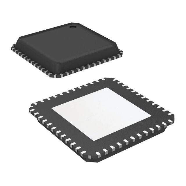


 工商网监
湘ICP备2023018690号
工商网监
湘ICP备2023018690号
