LMZ10501
www.ti.com
SNVS677C – MAY 2011 – REVISED SEPTEMBER 2012
LMZ10501 1A SIMPLE SWITCHER® Nano Module with 5.5V Maximum Input Voltage
Check for Samples: LMZ10501
FEATURES
1
•
•
2
•
•
•
•
•
•
•
Integrated inductor
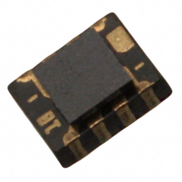
Miniature form factor (3.0 mm x 2.5 mm x 1.425
mm)
8-pin LLP footprint
-40°C to 125°C junction temperature range
Adjustable output voltage
2.0MHz fixed PWM switching frequency
Integrated compensation
Soft start function
Current limit protection
•
•
•
Thermal shutdown protection
Input voltage UVLO for power-up, powerdown, and brown-out conditions
Only 5 external components — resistor divider
and 3 ceramic capacitors
APPLICATIONS
•
•
•
Point of load conversions from 3.3V and 5V
rails
Space constrained applications
Low output noise applications
DESCRIPTION
The LMZ10501 SIMPLE SWITCHER® nano module is an easy-to-use step-down DC-DC solution capable of
driving up to 1A load in space-constrained applications. Only an input capacitor, an output capacitor, a small
VCON filter capacitor, and two resistors are required for basic operation. The nano module comes in 8-pin LLP
footprint package with an integrated inductor. Internal current limit based softstart function, current overload
protection, and thermal shutdown are also provided.
Electrical Specifications
•
•
•
•
Up to 1A output current
Input voltage range 2.7V to 5.5V
Output voltage range 0.6V to 3.6V
Efficiency up to 95%
Performance Benefits
•
•
•
•
Small solution size
Low output voltage ripple
Easy component selection and simple PCB layout
High efficiency reduces system heat generation
1
2
Please be aware that an important notice concerning availability, standard warranty, and use in critical applications of
Texas Instruments semiconductor products and disclaimers thereto appears at the end of this data sheet.
All trademarks are the property of their respective owners.
PRODUCTION DATA information is current as of publication date.
Products conform to specifications per the terms of the Texas
Instruments standard warranty. Production processing does not
necessarily include testing of all parameters.
Copyright © 2011–2012, Texas Instruments Incorporated
�LMZ10501
SNVS677C – MAY 2011 – REVISED SEPTEMBER 2012
www.ti.com
System Performance
(Quick Overview Links: VOUT = 1.2V, 1.8V, 2.5V, 3.3V)
Figure 1. Typical Efficiency at VIN = 3.6V
100
EFFICIENCY (%)
90
80
70
60
50
VOUT = 1.2V
VOUT = 1.8V
VOUT = 2.5V
VOUT = 3.3V
40
30
20
0.0 0.1 0.2 0.3 0.4 0.5 0.6 0.7 0.8 0.9 1.0
LOAD CURRENT (A)
Figure 2. Output Voltage Ripple
VIN = 5.0V, VOUT = 1.8V, IOUT = 1A
VOUT RIPPLE
COUT = 10 F 10V 0805 X5R
10 mV/Div
500 MHz BW
1 µs/Div
Figure 3. Radiated EMI (CISPR22)
VIN = 5.0V, VOUT = 1.8V, IOUT = 1A
RADIATED EMISSIONS (dB V/m)
80
Emissions (Evaluation Board)
EN 55022 Class B Limit
EN 55022 Class A Limit
70
60
50
40
30
20
10
0
0
2
200
400
600
800
FREQUENCY (MHz)
Submit Documentation Feedback
1000
Copyright © 2011–2012, Texas Instruments Incorporated
Product Folder Links: LMZ10501
�LMZ10501
www.ti.com
SNVS677C – MAY 2011 – REVISED SEPTEMBER 2012
Connection Diagram
PAD
PAD
PAD
Figure 4.
Table 1. Pin Descriptions
Pin #
Name
1
EN
2
VCON
Description
Enable Input. Set this digital input higher than 1.2V for normal operation. For shutdown, set low. Pin is
internally pulled up to VIN and can be left floating for always-on operation.
Output voltage control pin. Connect to analog voltage from resisitve divider or DAC/controller to set the VOUT
voltage. VOUT = 2.5 x VCON. Connect a small (470pF) capacitor from this pin to SGND to provide noise
filtering.
3
FB
4
SGND
Ground for analog and control circuitry. Connect to PGND at a single point.
5
VOUT
Output Voltage. Connected to one terminal of the integrated inductor. Connect output filter capacitor between
VOUT and PGND.
6
PGND
Power ground for the power MOSFETs and gate-drive circuitry.
7
VIN
8
VREF
PAD
Feedback of the error amplifier. Connect directly to output capacitor to sense VOUT.
Voltage supply input. Connect ceramic capacitor between VIN and PGND as close as possible to these two
pins. Typical capacitor values are between 4.7µF and 22µF.
2.35V voltage reference output. Typically connected to VCON pin through a resistive divider to set the output
voltage.
The 3 pads underneath the module are not internally connected to any node. These pads should be
connected to the ground plane for improved thermal performance.
These devices have limited built-in ESD protection. The leads should be shorted together or the device placed in conductive foam
during storage or handling to prevent electrostatic damage to the MOS gates.
Absolute Maximum Ratings
(1)
VIN, VREF to SGND
−0.2V to +6.0V
PGND to SGND
−0.2V to +0.2V
EN, FB, VCON
(SGND −0.2V)
to (VIN +0.2V)
w/6.0V max
VOUT
(PGND −0.2V)
to (VIN +0.2V)
w/6.0V max
Junction Temperature (TJ-MAX)
+150°C
Storage Temperature Range
−65°C to +150°C
Maximum Lead Temperature
+260°C
ESD Susceptibility
(1)
(2)
(2)
±2kV
Absolute Maximum Ratings are limits beyond which damage to the device may occur. Operating Ratings are conditions under which
operation of the device is intended to be functional. For guaranteed specifications and test conditions, see the Electrical Characteristics.
The human body model is a 100pF capacitor discharged through a 1.5 kΩ resistor into each pin. Test method is per JESD-22-114.
Submit Documentation Feedback
Copyright © 2011–2012, Texas Instruments Incorporated
Product Folder Links: LMZ10501
3
�LMZ10501
SNVS677C – MAY 2011 – REVISED SEPTEMBER 2012
Operating Ratings
www.ti.com
(1)
Input Voltage Range
2.7V to 5.5V
Recommended Load Current
0 mA to 1000 mA
Junction Temperature (TJ) Range
−40°C to +125°C
(1)
Absolute Maximum Ratings are limits beyond which damage to the device may occur. Operating Ratings are conditions under which
operation of the device is intended to be functional. For guaranteed specifications and test conditions, see the Electrical Characteristics.
Thermal Properties
Junction-to-Ambient Thermal
120°C/W
Resistance (θJA), SEA08A Package
(1)
(1)
4
Junction-to-ambient thermal resistance (θJA) is based on 4 layer board thermal measurements, performed under the conditions and
guidelines set forth in the JEDEC standards JESD51-1 to JESD51-11. θJA varies with PCB copper area, power dissipation, and airflow.
Submit Documentation Feedback
Copyright © 2011–2012, Texas Instruments Incorporated
Product Folder Links: LMZ10501
�LMZ10501
www.ti.com
SNVS677C – MAY 2011 – REVISED SEPTEMBER 2012
Electrical Characteristics
(1)
Specifications with standard typeface are for TJ = 25°C only; Limits in bold face type apply over the operating junction
temperature range TJ of -40°C to 125°C. Minimum and maximum limits are guaranteed through test, design, or statistical
correlation. Typical values represent the most likely parametric norm at TJ = 25°C, and are provided for reference purposes
only. Unless otherwise stated the following conditions apply: VIN = 3.6V, VEN = 1.2V.
Symbol
Parameter
Conditions
Min
Typ
Max
(1)
Units
(1)
(2)
SYSTEM PARAMETERS
VREF x GAIN
Reference voltage x VCON to
FB Gain
VIN = VEN = 5.5V, VCON = 1.44V
5.7575
5.875
5.9925
V
GAIN
VCON to FB Gain
VIN = 5.5V, VCON = 1.44V
2.4375
2.5
2.5750
V/V
VINUVLO
VIN rising threshold
2.4
V
VINUVLO
VIN falling theshold
2.25
V
ISHDN
Shutdown supply current
VIN = 3.6V, VEN = 0.5V
(3)
11
18
µA
Iq
DC bias current into VIN
VIN = 5.5V, VCON = 1.6V, IOUT =
0A
6.5
8.5
mA
RDROPOUT
VIN to VOUTresistance
IOUT = 200 mA
285
425
mΩ
I LIM
DC Output Current Limit
VCON = 0.24V
FOSC
2.25
MHz
(4)
1125
1350
Internal oscillator frequency
1.75
2.0
VIH,ENABLE
Enable logic HIGH voltage
1.2
VIL,ENABLE
Enable logic LOW voltage
TSD
Thermal shutdown
TSD-HYST
DMAX
mA
V
0.5
V
150
°C
Thermal shutdown hysteresis
20
°C
Maximum duty cycle
100
%
TON-MIN
Minimum on-time
50
ns
θJA
Package Thermal Resistance
(1)
(2)
(3)
(4)
Rising Threshold
20mm x 20mm board
2 layers, 2 oz copper, 0.5W, no
airlow
118
15mm x 15mm board
2 layers, 2 oz copper, 0.5W, no
airlow
132
10mm x 10mm board
2 layers, 2 oz copper, 0.5W, no
airlow
157
°C/W
Min and Max limits are 100% production tested at 25°C. Limits over the operating temperature range are guaranteed through correlation
using Statistical Quality Control (SQC) methods. Limits are used to calculate the Average Outgoing Quality Level (AOQL).
Typical numbers are at 25°C and represent the most likely parametric norm.
Shutdown current includes leakage current of the high side PFET.
Current limit is built-in, fixed, and not adjustable.
Submit Documentation Feedback
Copyright © 2011–2012, Texas Instruments Incorporated
Product Folder Links: LMZ10501
5
�LMZ10501
SNVS677C – MAY 2011 – REVISED SEPTEMBER 2012
www.ti.com
System Characteristics
The following specifications are guaranteed by design providing the component values in the Typical Application Circuit are
used (CIN = COUT = 10 µF, 6.3V, 0603, TDK C1608X5R0J106K). These parameters are not guaranteed by production
testing. Unless otherwise stated the following conditions apply: TA = 25°C.
Symbol
Parameter
Conditions
Min
Typ
Max
Units
ΔVOUT/VOUT Output Voltage Regulation Over
Line Voltage and Load Current
VOUT = 0.6V
ΔVIN =2.7V to 4.2V
ΔIOUT = 0A to 1A
±1.75
%
ΔVOUT/VOUT Output Voltage Regulation Over
Line Voltage and Load Current
VOUT = 1.5V
ΔVIN = 2.7V to 5.5V
ΔIOUT = 0A to 1A
±0.92
%
ΔVOUT/VOUT Output Voltage Regulation Over
Line Voltage and Load Current
VOUT = 3.6V
ΔVIN = 4.0V to 5.5V
ΔIOUT = 0A to 1A
±0.38
%
VREF TRISE Rise time of reference voltage
EN = Low to High, VIN = 4.2V
VOUT = 2.7V, IOUT = 1A
10
µs
VIN = 5.0V, VOUT = 3.3V
IOUT = 200 mA
95
VIN = 5.0V, VOUT = 3.6V
IOUT = 1000 mA
91
VIN = 5.0V, VOUT = 1.8V
IOUT = 1000 mA (1)
10
mV pk-pk
Line transient response
VIN = 2.7V to 5.5V,
TR = TF= 10 µs,
VOUT = 1.8V, IOUT = 1000mA
30
mV pk-pk
Load transient response
VIN = 5.0V
TR = TF = 40 µs,
VOUT = 1.8V
IOUT = 100mA to 1000 mA
30
mV pk-pk
Peak Efficiency
η
Full Load Efficiency
VOUT Ripple Output voltage ripple
Line
Transient
Load
Transient
(1)
6
%
Ripple voltage should be measured across COUT on a well-designed PC board using the suggested capacitors.
Submit Documentation Feedback
Copyright © 2011–2012, Texas Instruments Incorporated
Product Folder Links: LMZ10501
�LMZ10501
www.ti.com
SNVS677C – MAY 2011 – REVISED SEPTEMBER 2012
Typical Performance Characteristics
Unless otherwise specified the following conditions apply: VIN = 3.6V, TA = 25°C
Dropout Voltage
vs
Load Current and Input Voltage
Thermal Derating VOUT = 1.2V, θJA = 120°C/W
0.30
0.25
1.2
VIN = 2.7V
VIN = 3.3V
VIN = 3.6V
VIN = 4.0V
OUTPUT CURRENT (A)
DROPOUT VOLTAGE (V)
0.35
0.20
0.15
0.10
0.00
0.4
1.0
60
70 80 90 100 110 120 130
AMBIENT TEMPERATURE (°C)
Thermal Derating VOUT = 2.5V, θJA = 120°C/W
1.2
1.2
VIN = 3.3V
VIN = 3.6V
VIN = 5.0V
VIN = 5.5V
1.0
OUTPUT CURRENT (A)
OUTPUT CURRENT (A)
0.6
0.0
0.2
0.4
0.6
0.8
LOAD CURRENT (A)
Thermal Derating VOUT = 1.8V, θJA = 120°C/W
0.8
0.6
0.4
0.2
VIN = 3.3V
VIN = 3.6V
VIN = 5.0V
VIN = 5.5V
1.0
0.8
0.6
0.4
0.2
0.0
0.0
60
70 80 90 100 110 120 130
AMBIENT TEMPERATURE (°C)
60
1.2
80
1.0
RADIATED EMISSIONS (dB V/m)
VIN = 4.0V
VIN = 4.5V
VIN = 5.0V
VIN = 5.5V
0.8
0.6
0.4
0.2
70 80 90 100 110 120 130
AMBIENT TEMPERATURE (°C)
Radiated EMI (CISPR22)
VIN = 5.0V, VOUT = 1.8V, IOUT = 1A
Default evaluation board BOM
Thermal Derating VOUT = 3.3V, θJA = 120°C/W
OUTPUT CURRENT (A)
0.8
0.2
0.05
0.0
VIN = 3.3V
VIN = 3.6V
VIN = 5.0V
VIN = 5.5V
1.0
0.0
Emissions (Evaluation Board)
EN 55022 Class B Limit
EN 55022 Class A Limit
70
60
50
40
30
20
10
0
60
70 80 90 100 110 120 130
AMBIENT TEMPERATURE (°C)
0
200
400
600
800
FREQUENCY (MHz)
1000
Submit Documentation Feedback
Copyright © 2011–2012, Texas Instruments Incorporated
Product Folder Links: LMZ10501
7
�LMZ10501
SNVS677C – MAY 2011 – REVISED SEPTEMBER 2012
www.ti.com
Typical Performance Characteristics (continued)
Unless otherwise specified the following conditions apply: VIN = 3.6V, TA = 25°C
Conducted EMI
VIN = 5.0V, VOUT = 1.8V, IOUT = 1A
Default evaluation board BOM with additional 1µH 1µF LC
input filter
CONDUCTED EMISSIONS (dB V)
80
70
Startup
VCON
Conducted Emissions
CISPR 22 Quasi Peak
CISPR 22 Average
500 mV/Div
60
50
300 mA/Div
IL
40
300 mA/Div
30
20
10
IOUT
500 mV/Div
VOUT
10 µs/Div
0
100m
8
1
10
FREQUENCY (MHz)
100
Submit Documentation Feedback
Copyright © 2011–2012, Texas Instruments Incorporated
Product Folder Links: LMZ10501
�LMZ10501
www.ti.com
SNVS677C – MAY 2011 – REVISED SEPTEMBER 2012
1.2V
Schematic VOUT = 1.2V
VIN
CIN
EN
VIN
Efficiency VOUT = 1.2V
100
1.2V
VOUT
90
VOUT
VREF
VCON
PGND
RB
EFFICIENCY (%)
FB
RT
COUT
SGND
CVC
CIN
COUT
CVC
RT
RB
10 P) 8 6.3V
10 PF 8 6.3V
470 pF 8 6.3V
243 k: 1%
63.4 k: 1%
0805 X7R or X5R
0805 X7R or X5R
0603 X7R or X5R
0603
0603
80
70
60
50
VIN = 2.7V
VIN = 3.3V
VIN = 3.6V
VIN = 5.0V
VIN = 5.5V
40
30
20
0.0 0.1 0.2 0.3 0.4 0.5 0.6 0.7 0.8 0.9 1.0
LOAD CURRENT (A)
Output Ripple VOUT = 1.2V
Load Transient VOUT = 1.2V
COUT = 10 F 10V 0805 X5R
VOUT RIPPLE
COUT = 10 F 10V 0805 X5R
30 mV/Div
OUTPUT VOLTAGE
10 mV/Div
500 mA/Div
500 MHz BW
1 µs/Div
Line and Load Regulation VOUT = 1.2V
1.5
DC CURRENT LIMIT (A)
OUTPUT VOLTAGE (V)
500 µs/Div
DC Current Limit VOUT = 1.2V
1.24
1.23
1.22
1.21
LOAD CURRENT
250 MHz BW
VIN = 2.7V
VIN = 3.3V
VIN = 3.6V
VIN = 5.0V
VIN = 5.5V
1.20
0.0 0.1 0.2 0.3 0.4 0.5 0.6 0.7 0.8 0.9 1.0
LOAD CURRENT (A)
TA= 85°C
1.4
1.3
1.2
1.1
1.0
2.5
3.0
3.5
4.0
4.5
5.0
INPUT VOLTAGE (V)
5.5
Submit Documentation Feedback
Copyright © 2011–2012, Texas Instruments Incorporated
Product Folder Links: LMZ10501
9
�LMZ10501
SNVS677C – MAY 2011 – REVISED SEPTEMBER 2012
www.ti.com
1.8V
Schematic VOUT = 1.8V
VIN
CIN
EN
VIN
Efficiency VOUT = 1.8V
100
1.8V
VOUT
90
VOUT
VREF
VCON
PGND
RB
EFFICIENCY (%)
FB
RT
COUT
SGND
CVC
CIN
COUT
CVC
RT
RB
10 P) 8 6.3V
10 PF 8 6.3V
470 pF 8 6.3V
187 k: 1%
82.5 k: 1%
0805 X7R or X5R
0805 X7R or X5R
0603 X7R or X5R
0603
0603
80
70
60
50
VIN = 2.7V
VIN = 3.3V
VIN = 3.6V
VIN = 5.0V
VIN = 5.5V
40
30
20
0.0 0.1 0.2 0.3 0.4 0.5 0.6 0.7 0.8 0.9 1.0
LOAD CURRENT (A)
Output Ripple VOUT = 1.8V
Load Transient VOUT = 1.8V
COUT = 10 F 10V 0805 X5R
VOUT RIPPLE
COUT = 10 F 10V 0805 X5R
30 mV/Div
OUTPUT VOLTAGE
500 mA/Div
LOAD CURRENT
10 mV/Div
1 µs/Div
500 MHz BW
250 MHz BW
Line and Load Regulation VOUT = 1.8V
DC Current Limit VOUT = 1.8V
1.5
DC CURRENT LIMIT (A)
OUTPUT VOLTAGE (V)
1.81
1.80
1.79
1.78
VIN = 2.7V
VIN = 3.3V
VIN = 3.6V
VIN = 5.0V
VIN = 5.5V
1.77
0.0 0.1 0.2 0.3 0.4 0.5 0.6 0.7 0.8 0.9 1.0
LOAD CURRENT (A)
10
500 µs/Div
Submit Documentation Feedback
TA= 85°C
1.4
1.3
1.2
1.1
1.0
2.5
3.0
3.5
4.0
4.5
5.0
INPUT VOLTAGE (V)
5.5
Copyright © 2011–2012, Texas Instruments Incorporated
Product Folder Links: LMZ10501
�LMZ10501
www.ti.com
SNVS677C – MAY 2011 – REVISED SEPTEMBER 2012
2.5V
Schematic VOUT = 2.5V
VIN
CIN
EN
VIN
Efficiency VOUT = 2.5V
100
2.5V
VOUT
90
VOUT
VREF
VCON
PGND
RB
EFFICIENCY (%)
FB
RT
COUT
SGND
CVC
CIN
COUT
CVC
RT
RB
10 P) 8 6.3V
10 PF 8 6.3V
470 pF 8 6.3V
150 k: 1%
118 k: 1%
0805 X7R or X5R
0805 X7R or X5R
0603 X7R or X5R
0603
0603
80
70
60
50
VIN = 3.3V
VIN = 3.6V
VIN = 5.0V
VIN = 5.5V
40
30
20
0.0 0.1 0.2 0.3 0.4 0.5 0.6 0.7 0.8 0.9 1.0
LOAD CURRENT (A)
Output Ripple VOUT = 2.5V
Load Transient VOUT = 2.5V
COUT = 10 F 10V 0805 X5R
VOUT RIPPLE
COUT = 10 PF 10V 0805 X5R
30 mV/Div
OUTPUT VOLTAGE
10 mV/Div
500 mA/Div
500 MHz BW
LOAD CURRENT
1 Ps/Div
250 MHz BW
Line and Load Regulation VOUT = 2.5V
DC Current Limit VOUT = 2.5V
1.5
DC CURRENT LIMIT (A)
OUTPUT VOLTAGE (V)
2.53
2.52
2.51
2.50
2.50
500 µs/Div
VIN = 3.3V
VIN = 3.6V
VIN = 5.0V
VIN = 5.5V
0.0 0.1 0.2 0.3 0.4 0.5 0.6 0.7 0.8 0.9 1.0
LOAD CURRENT (A)
TA= 85°C
1.4
1.3
1.2
1.1
1.0
2.5
3.0
3.5
4.0
4.5
5.0
INPUT VOLTAGE (V)
5.5
Submit Documentation Feedback
Copyright © 2011–2012, Texas Instruments Incorporated
Product Folder Links: LMZ10501
11
�LMZ10501
SNVS677C – MAY 2011 – REVISED SEPTEMBER 2012
www.ti.com
3.3V
Schematic VOUT = 3.3V
VIN
CIN
EN
VIN
Efficiency VOUT = 3.3V
100
3.3V
VOUT
90
VOUT
VREF
VCON
RB
CIN
COUT
CVC
RT
RB
PGND
EFFICIENCY (%)
FB
RT
COUT
SGND
CVC
10 P) 8 6.3V
10 PF 8 6.3V
470 pF 8 6.3V
118 k: 1%
150 k: 1%
0805 X7R or X5R
0805 X7R or X5R
0603 X7R or X5R
0603
0603
80
70
60
50
VIN = 3.6V
VIN = 4.0V
VIN = 4.5V
VIN = 5.0V
VIN = 5.5V
40
30
20
0.0 0.1 0.2 0.3 0.4 0.5 0.6 0.7 0.8 0.9 1.0
LOAD CURRENT (A)
Output Ripple VOUT = 3.3V
Load Transient VOUT = 3.3V
COUT = 10 F 10V 0805 X5R
VOUT RIPPLE
COUT = 10 F 10V 0805 X5R
30 mV/Div
OUTPUT VOLTAGE
10 mV/Div
500 mA/Div
500 MHz BW
1 µs/Div
Line and Load Regulation VOUT = 3.3V
DC CURRENT LIMIT (A)
OUTPUT VOLTAGE (V)
1.5
3.28
3.26
VIN = 3.6V
VIN = 4.0V
VIN = 4.5V
VIN = 5.0V
VIN = 5.5V
3.22
0.0 0.1 0.2 0.3 0.4 0.5 0.6 0.7 0.8 0.9 1.0
LOAD CURRENT (A)
12
500 µs/Div
DC Current Limit VOUT = 3.3V
3.30
3.24
LOAD CURRENT
250 MHz BW
Submit Documentation Feedback
TA= 85°C
1.4
1.3
1.2
1.1
1.0
2.5
3.0
3.5
4.0
4.5
5.0
INPUT VOLTAGE (V)
5.5
Copyright © 2011–2012, Texas Instruments Incorporated
Product Folder Links: LMZ10501
�LMZ10501
www.ti.com
SNVS677C – MAY 2011 – REVISED SEPTEMBER 2012
BLOCK DIAGRAM
VREF
VIN
UVLO
REFERENCE
VOLTAGE
VCON
ERROR
AMPLIFIER
FB
COMP
CURRENT
COMP
CURRENT SENSE
L
VOUT
MOSFET
CONTROL
LOGIC
Integrated
Inductor
VIN
UVLO
MAIN CONTROL
EN
TSD
OSCILLATOR
SGND
PGND
Figure 5. Functional Block Diagram
Overview
The LMZ10501 SIMPLE SWITCHER® nano module is an easy-to-use step-down DC-DC solution capable of
driving up to 1A load in space-constrained applications. Only an input capacitor, an output capacitor, a small
VCON filter capacitor, and two resistors are required for basic operation. The nano module comes in 8-pin LLP
footprint package with an integrated inductor. The LMZ10501 operates in fixed 2.0MHz PWM (Pulse Width
Modulation) mode, and is designed to deliver power at maximum efficiency. The output voltage is typically set by
using a resistive divider between the built-in reference voltage VREF and the control pin VCON. The VCON pin is the
positive input to the error amplifier. The output voltage of the LMZ10501 can also be dynamically adjusted
between 0.6V and 3.6V by driving the VCON pin externally. Internal current limit based softstart function, current
overload protection, and thermal shutdown are also provided.
CIRCUIT OPERATION
The LMZ10501 is a synchronous Buck power module using a PFET for the high side switch and an NFET for the
synchronous rectifier switch. The output voltage is regulated by modulating the PFET switch on-time. The circuit
generates a duty-cycle modulated rectangular signal. The rectangular signal is averaged using a low pass filter
formed by the integrated inductor and an output capacitor. The output voltage is equal to the average of the dutycycle modulated rectangular signal. In PWM mode, the switching frequency is constant. The energy per cycle to
the load is controlled by modulating the PFET on-time, which controls the peak inductor current. In current mode
control architecture, the inductor current is compared with the slope compensated output of the error amplifier. At
the rising edge of the clock, the PFET is turned ON, ramping up the inductor current with a slope of (VIN VOUT)/L. The PFET is ON until the current signal equals the error signal. Then the PFET is turned OFF and
NFET is turned ON, ramping down the inductor current with a slope of VOUT /L. At the next rising edge of the
clock, the cycle repeats. An increase of load pulls the output voltage down, resulting in an increase of the error
signal. As the error signal goes up, the peak inductor current is increased, elevating the average inductor current
and responding to the heavier load. To ensure stability, a slope compensation ramp is subtracted from the error
signal and internal loop compensation is provided.
Submit Documentation Feedback
Copyright © 2011–2012, Texas Instruments Incorporated
Product Folder Links: LMZ10501
13
�LMZ10501
SNVS677C – MAY 2011 – REVISED SEPTEMBER 2012
www.ti.com
INPUT UNDER VOLTAGE DETECTION
The LMZ10501 implements an under voltage lock out (UVLO) circuit to ensure proper operation during startup,
shutdown and input supply brownout conditions. The circuit monitors the voltage at the VIN pin to ensure that
sufficient voltage is present to bias the regulator. If the under voltage threshold is not met, all functions of the
controller are disabled and the controller remains in a low power standby state.
SHUTDOWN MODE
To shutdown the LMZ10501, pull the EN pin low (


 工商网监
湘ICP备2023018690号
工商网监
湘ICP备2023018690号
