Product
Folder
Order
Now
Support &
Community
Tools &
Software
Technical
Documents
Reference
Design
LMZ31503
SNVS992B – JULY 2013 – REVISED APRIL 2018
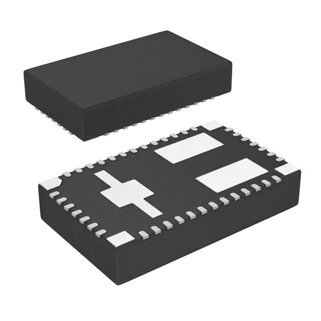
LMZ31503 3-A Power Module With 4.5-V to 14.5-V Input
in QFN Package
1 Features
3 Description
•
The LMZ31503 power module is an easy-to-use
integrated power solution that combines a 3-A DC/DC
converter with power MOSFETs, a shielded inductor,
and passives into a low profile, QFN package. This
total power solution allows as few as 3 external
components and eliminates the loop compensation
and magnetics design process.
1
•
•
•
•
•
•
•
•
•
•
•
•
•
•
•
•
•
Complete Integrated Power Solution Allows
Small Footprint, Low-Profile Design
9 mm × 15mm × 2.8mm package
- Pin Compatible with LMZ31506
Efficiencies Up To 95%
Wide-Output Voltage Adjust
0.8 V to 5.5 V, with 1% Reference Accuracy
Optional Split Power Rail Allows
Input Voltage Down to 1.6 V
Adjustable Switching Frequency
(330 kHz to 780 kHz)
Synchronizes to an External Clock
Adjustable Slow-Start
Output Voltage Sequencing / Tracking
Power Good Output
Programmable Undervoltage Lockout (UVLO)
Overcurrent Protection (Hiccup-Mode)
Over Temperature Protection
Pre-bias Output Start-up
Operating Temperature Range: –40°C to +85°C
Enhanced Thermal Performance: 13°C/W
Meets EN55022 Class B Emissions
- Integrated Shielded Inductor
Create a Custom Design Using the LMZ31503
With the WEBENCH® Power Designer
The 9×15×2.8 mm QFN package is easy to solder
onto a printed circuit board and allows a compact
point-of-load design with up to 95% efficiency and
excellent power dissipation with a thermal impedance
of 13°C/W junction to ambient. The device delivers
the full 3-A rated output current at 85°C ambient
temperature without airflow.
The LMZ31503 offers the flexibility and the featureset of a discrete point-of-load design and is ideal for
powering performance DSPs and FPGAs. Advanced
packaging technology afford a robust and reliable
power solution compatible with standard QFN
mounting and testing techniques.
Simplified Schematic
LMZ31503
PVIN
PWRGD
VIN
VOUT
VIN
CIN
VOUT
2 Applications
RT/CLK
•
•
•
•
•
INH/UVLO
Broadband & Communications Infrastructure
Automated Test and Medical Equipment
Compact PCI / PCI Express / PXI Express
DSP and FPGA Point of Load Applications
High Density Distributed Power Systems
COUT
SENSE+
SS/TR
VADJ
STSEL
PGND AGND
RSET
Efficiency (%)
Efficiency
100
95
90
85
80
75
70
65
60
55
50
45
40
VIN = PVIN = 5 V, VOUT = 3.3V, fSW = 630 kHz
VIN = PVIN = 12 V, VOUT = 3.3V, fSW = 630 kHz
0
0.5
1
1.5
2
Output Current (A)
2.5
3
G000
1
An IMPORTANT NOTICE at the end of this data sheet addresses availability, warranty, changes, use in safety-critical applications,
intellectual property matters and other important disclaimers. PRODUCTION DATA.
�LMZ31503
SNVS992B – JULY 2013 – REVISED APRIL 2018
www.ti.com
4 Specifications
4.1
Absolute Maximum Ratings (1)
over operating temperature range (unless otherwise noted)
Input Voltage
Output Voltage
VALUE
UNIT
VIN
–0.3 to 16
V
PVIN
–0.3 to 16
V
INH/UVLO
–0.3 to 6
V
VADJ
–0.3 to 3
V
PWRGD
–0.3 to 6
V
SS/TR
–0.3 to 3
V
STSEL
–0.3 to 3
V
RT/CLK
–0.3 to 6
V
PH
–1 to 20
V
PH 10ns Transient
–3 to 20
V
–0.2 to 0.2
V
VDIFF (GND to exposed thermal pad)
RT/CLK
Source Current
Sink Current
±100
µA
PH
Current Limit
A
PH
Current Limit
A
PVIN
Current Limit
A
–0.1 to 5
mA
–40 to 125 (2)
°C
–65 to 150
°C
245 (4)
°C
PWRGD
Operating Junction Temperature
Storage Temperature
Peak Reflow Case Temperature (3)
Maximum Number of Reflows Allowed (3)
3 (4)
Mechanical Shock
Mil-STD-883D, Method 2002.3, 1 msec, 1/2 sine, mounted
Mechanical Vibration
Mil-STD-883D, Method 2007.2, 20-2000Hz
(1)
(2)
(3)
(4)
2
1500
G
20
Stresses beyond those listed under absolute maximum ratings may cause permanent damage to the device. These are stress ratings
only, and functional operation of the device at these or any other conditions beyond those indicated under recommended operating
conditions is not implied. Exposure to absolute-maximum-rated conditions for extended periods may affect device reliability.
See the temperature derating curves in the Typical Characteristics section for thermal information.
For soldering specifications, refer to the Soldering Requirements for BQFN Packages application note.
Devices with a date code prior to week 14 2018 (1814) have a peak reflow case temperature of 240°C with a maximum of one reflow
Submit Documentation Feedback
Copyright © 2013–2018, Texas Instruments Incorporated
Product Folder Links: LMZ31503
�LMZ31503
www.ti.com
SNVS992B – JULY 2013 – REVISED APRIL 2018
4.2 Thermal Information
LMZ31503
THERMAL METRIC (1)
RUQ47
UNIT
47 PINS
Junction-to-ambient thermal resistance (2)
θJA
(3)
ψJT
Junction-to-top characterization parameter
ψJB
Junction-to-board characterization parameter (4)
(1)
13
°C/W
2.5
°C/W
5
°C/W
For more information about traditional and new thermal metrics, see the Semiconductor and IC Package Thermal Metrics application
report.
The junction-to-ambient thermal resistance, θJA, applies to devices soldered directly to a 100 mm x 100 mm double-sided PCB with 1 oz.
copper and natural convection cooling. Additional airflow reduces θJA.
The junction-to-top characterization parameter, ψJT, estimates the junction temperature, TJ, of a device in a real system, using a
procedure described in JESD51-2A (sections 6 and 7). TJ = ψJT * Pdis + TT; where Pdis is the power dissipated in the device and TT is
the temperature of the top of the device.
The junction-to-board characterization parameter, ψJB, estimates the junction temperature, TJ, of a device in a real system, using a
procedure described in JESD51-2A (sections 6 and 7). TJ = ψJB * Pdis + TB; where Pdis is the power dissipated in the device and TB is
the temperature of the board 1mm from the device.
(2)
(3)
(4)
4.3 Package Specifications
LMZ31503
UNIT
Weight
Flammability
MTBF Calculated reliability
4.4
1.26 grams
Meets UL 94 V-O
Per Bellcore TR-332, 50% stress, TA = 40°C, ground benign
40.1 MHrs
Electrical Characteristics
Over -40°C to 85°C free-air temperature, PVIN = VIN = 12 V, VOUT = 1.8 V, IOUT = 3A,
CIN1 = 2x 22 µF ceramic, CIN2 = 68 µF poly-tantalum, COUT1 = 4x 47 µF ceramic (unless otherwise noted)
PARAMETER
TEST CONDITIONS
MIN
TYP
MAX
UNIT
IOUT
Output current
TA = 85°C, natural convection
0
3
A
VIN
Input bias voltage range
Over IOUT range
4.5
14.5
V
PVIN
Input switching voltage range
Over IOUT range
1.6 (1)
14.5
V
UVLO
VIN Undervoltage lockout
VOUT(adj)
VOUT
VIN = increasing
4.0
VIN = decreasing
3.5
Output voltage adjust range
Over IOUT range
0.8
Set-point voltage tolerance
TA = 25°C, IOUT = 0A
Temperature variation
-40°C ≤ TA ≤ +85°C, IOUT = 0A
±0.3%
Line regulation
Over PVIN range, TA = 25°C, IOUT = 0A
±0.1%
Load regulation
Over IOUT range, TA = 25°C
±0.1%
Total output voltage variation
Includes set-point, line, load, and temperature variation
PVIN = VIN = 12 V
IO = 1.5 A
η
Efficiency
PVIN = VIN = 5 V
IO = 1.5 A
Output voltage ripple
ILIM
(1)
(2)
3.85
5.5
VOUT = 5V, fSW = 780kHz
91.5 %
VOUT = 3.3V, fSW = 630kHz
89.0 %
VOUT = 2.5V, fSW = 480kHz
86.9 %
VOUT = 1.8V, fSW = 480kHz
85.2 %
VOUT = 1.2V, fSW = 480kHz
82.1 %
VOUT = 0.8V, fSW = 330kHz
78.7 %
VOUT = 3.3V, fSW = 630kHz
93.3 %
VOUT = 2.5V, fSW = 480kHz
91.4 %
VOUT = 1.8V, fSW = 480kHz
88.8 %
VOUT = 1.2V, fSW = 480kHz
85.2 %
VOUT = 0.8V, fSW = 330kHz
81.8 %
20 MHz bandwith
Overcurrent threshold
4.5
±1.0%
(2)
±1.5%
(2)
V
V
35
mVPP
5.8
A
The minimum PVIN voltage is 1.6V or (VOUT+ 0.7V) , whichever is greater. VIN must be greater than 4.5V.
The stated limit of the set-point voltage tolerance includes the tolerance of both the internal voltage reference and the internal
adjustment resistor. The overall output voltage tolerance will be affected by the tolerance of the external RSET resistor.
Submit Documentation Feedback
Copyright © 2013–2018, Texas Instruments Incorporated
Product Folder Links: LMZ31503
3
�LMZ31503
SNVS992B – JULY 2013 – REVISED APRIL 2018
www.ti.com
Electrical Characteristics (continued)
Over -40°C to 85°C free-air temperature, PVIN = VIN = 12 V, VOUT = 1.8 V, IOUT = 3A,
CIN1 = 2x 22 µF ceramic, CIN2 = 68 µF poly-tantalum, COUT1 = 4x 47 µF ceramic (unless otherwise noted)
PARAMETER
Transient response
VINH-H
VINH-L
II(stby)
Inhibit Control
TEST CONDITIONS
1.0 A/µs load step from 50 to 100% IOUT(max)
MIN
190
VOUT
over/undershoot
35
Inhibit High Voltage
1.30
Inhibit Low Voltage
–0.3
INH < 1.1 V
-1.15
INH > 1.26 V
-3.4
Input standby current
INH pin to AGND
2
VOUT falling
PWRGD Low Voltage
I(PWRGD) = 2 mA
fSW
Switching frequency
Over VIN and IOUT ranges, RT/CLK pin OPEN
fCLK
Synchronization frequency
VCLK-H
CLK High-Level Threshold
VCLK-L
CLK Low-Level Threshold
DCLK
CLK Duty cycle
Thermal Shutdown
CIN
(4)
(5)
4
Fault
91%
Good
106%
μA
4
µA
V
330
780
kHz
2.0
5.5
V
0.8
V
22
330
80%
175
°C
10
°C
(4)
µF
68 (4)
200
Non-ceramic
μA
kHz
160
Non-ceramic
V
0.3
Thermal shutdown hysteresis
Ceramic
mV
(3)
390
270
Thermal shutdown
(5)
1500
5000
Equivalent series resistance (ESR)
(3)
109%
20%
Ceramic
External output capacitance
94%
Fault
CLK Control
External input capacitance
COUT
Good
UNIT
µs
1.05
INH Hysteresis current
PWRGD Thresholds
MAX
Open
INH Input current
VOUT rising
Power
Good
TYP
Recovery time
35
µF
mΩ
This control pin has an internal pullup. If this pin is left open circuit, the device operates when input power is applied. A small lowleakage ( 4.5 V
VIN
PVIN
RUVLO1
INH/UVLO
RUVLO2
Figure 42. Adjustable PVIN Undervoltage Lockout, (VIN ≥4.5 V)
Table 9. Standard Resistor Values for Adjusting PVIN UVLO, (VIN ≥4.5 V)
PVIN UVLO (V)
24
2.0
2.5
3.0
3.5
4.0
4.5
RUVLO1 (kΩ)
68.1
68.1
68.1
68.1
68.1
68.1
RUVLO2 (kΩ)
95.3
60.4
44.2
34.8
28.7
24.3
Hysteresis (mV)
300
315
335
350
365
385
Submit Documentation Feedback
For higher PVIN UVLO voltages see
Table UV for resistor values
Copyright © 2013–2018, Texas Instruments Incorporated
Product Folder Links: LMZ31503
�LMZ31503
www.ti.com
SNVS992B – JULY 2013 – REVISED APRIL 2018
9.17 Thermal Shutdown
The internal thermal shutdown circuitry forces the device to stop switching if the junction temperature exceeds
175°C typically. The device reinitiates the power up sequence when the junction temperature drops below 165°C
typically.
9.18 Layout Considerations
To achieve optimal electrical and thermal performance, an optimized PCB layout is required. Figure 43 and
Figure 44 show two layers of a typical PCB layout. Some considerations for an optimized layout are:
• Use large copper areas for power planes (VIN, VOUT, and PGND) to minimize conduction loss and thermal
stress.
• Place ceramic input and output capacitors close to the module pins to minimize high frequency noise.
• Locate additional output capacitors between the ceramic capacitor and the load.
• Place a dedicated AGND copper area beneath the LMZ31503.
• Isolate the PH copper area from the VOUT copper area using the AGND copper area.
• Connect the AGND and PGND copper area at one point; near the output capacitors.
• Place RSET, RRT, and CSS as close as possible to their respective pins.
• Use multiple vias to connect the power planes to internal layers.
SENSE+
Via
SENSE+
Via
VOUT
COUT3
PGND
Plane
COUT2
COUT1
Vias to
Topside
PGND
Copper
RRT
PGND
AGND to PGND
connection
CIN1
CIN2
Vias to
Topside
AGND
Copper
AGND
AGND
Plane
PH
SENSE+
Via
RSET
VIN/PVIN
SENSE+
Via
CSS
Figure 43. Typical Top-Layer Recommended Layout
Figure 44. Typical GND-Layer Recommended Layout
Submit Documentation Feedback
Copyright © 2013–2018, Texas Instruments Incorporated
Product Folder Links: LMZ31503
25
�LMZ31503
SNVS992B – JULY 2013 – REVISED APRIL 2018
www.ti.com
9.19 EMI
The LMZ31503 is compliant with EN55022 Class B radiated emissions. Figure 45 and Figure 46 show typical
examples of radiated emissions plots for the LMZ31503 operating from 5V and 12V respectively. Both graphs
include the plots of the antenna in the horizontal and vertical positions.
Figure 45. Radiated Emissions 5-V Input, 1.2-V Output, 3-A
Load (EN55022 Class B)
26
Figure 46. Radiated Emissions 12-V Input, 1.2-V Output, 3A Load (EN55022 Class B)
Submit Documentation Feedback
Copyright © 2013–2018, Texas Instruments Incorporated
Product Folder Links: LMZ31503
�LMZ31503
www.ti.com
SNVS992B – JULY 2013 – REVISED APRIL 2018
10 Revision History
NOTE: Page numbers for previous revisions may differ from page numbers in the current version.
Changes from Revision A (June 2017) to Revision B
Page
•
Added WEBENCH® design links for the LMZ31503.............................................................................................................. 1
•
Increased the peak reflow temperature and maximum number of reflows to JEDEC specifications for improved
manufacturability..................................................................................................................................................................... 2
•
Added Device Support section ............................................................................................................................................. 28
•
Added Mechanical, Packaging, and Orderable Information section .................................................................................... 29
Changes from Original (July 2013) to Revision A
•
Page
Added peak reflow and maximum number of reflows information ........................................................................................ 2
Submit Documentation Feedback
Copyright © 2013–2018, Texas Instruments Incorporated
Product Folder Links: LMZ31503
27
�LMZ31503
SNVS992B – JULY 2013 – REVISED APRIL 2018
www.ti.com
11 Device and Documentation Support
11.1 Device Support
11.1.1 Development Support
11.1.1.1 Custom Design With WEBENCH® Tools
Click here to create a custom design using the LMZ31503 device with the WEBENCH® Power Designer.
1. Start by entering the input voltage (VIN), output voltage (VOUT), and output current (IOUT) requirements.
2. Optimize the design for key parameters such as efficiency, footprint, and cost using the optimizer dial.
3. Compare the generated design with other possible solutions from Texas Instruments.
The WEBENCH Power Designer provides a customized schematic along with a list of materials with real-time
pricing and component availability.
In most cases, these actions are available:
• Run electrical simulations to see important waveforms and circuit performance
• Run thermal simulations to understand board thermal performance
• Export customized schematic and layout into popular CAD formats
• Print PDF reports for the design, and share the design with colleagues
Get more information about WEBENCH tools at www.ti.com/WEBENCH.
11.2 Documentation Support
11.2.1 Related Documentation
For related documentation see the following:
Soldering Requirements for BQFN Packages
11.3 Receiving Notification of Documentation Updates
To receive notification of documentation updates, navigate to the device product folder on ti.com. In the upper
right corner, click on Alert me to register and receive a weekly digest of any product information that has
changed. For change details, review the revision history included in any revised document.
11.4 Community Resources
The following links connect to TI community resources. Linked contents are provided "AS IS" by the respective
contributors. They do not constitute TI specifications and do not necessarily reflect TI's views; see TI's Terms of
Use.
TI E2E™ Online Community TI's Engineer-to-Engineer (E2E) Community. Created to foster collaboration
among engineers. At e2e.ti.com, you can ask questions, share knowledge, explore ideas and help
solve problems with fellow engineers.
Design Support TI's Design Support Quickly find helpful E2E forums along with design support tools and
contact information for technical support.
11.5 Trademarks
E2E is a trademark of Texas Instruments.
WEBENCH is a registered trademark of Texas Instruments.
All other trademarks are the property of their respective owners.
11.6 Electrostatic Discharge Caution
This integrated circuit can be damaged by ESD. Texas Instruments recommends that all integrated circuits be handled with
appropriate precautions. Failure to observe proper handling and installation procedures can cause damage.
ESD damage can range from subtle performance degradation to complete device failure. Precision integrated circuits may be more
susceptible to damage because very small parametric changes could cause the device not to meet its published specifications.
28
Submit Documentation Feedback
Copyright © 2013–2018, Texas Instruments Incorporated
Product Folder Links: LMZ31503
�LMZ31503
www.ti.com
SNVS992B – JULY 2013 – REVISED APRIL 2018
11.7 Glossary
SLYZ022 — TI Glossary.
This glossary lists and explains terms, acronyms, and definitions.
12 Mechanical, Packaging, and Orderable Information
The following pages include mechanical, packaging, and orderable information. This information is the most
current data available for the designated devices. This data is subject to change without notice and revision of
this document. For browser-based versions of this data sheet, refer to the left-hand navigation.
12.1 Tape and Reel Information
REEL DIMENSIONS
TAPE DIMENSIONS
K0
P1
B0 W
Reel
Diameter
Cavity
A0
B0
K0
W
P1
A0
Dimension designed to accommodate the component width
Dimension designed to accommodate the component length
Dimension designed to accommodate the component thickness
Overall width of the carrier tape
Pitch between successive cavity centers
Reel Width (W1)
QUADRANT ASSIGNMENTS FOR PIN 1 ORIENTATION IN TAPE
Sprocket Holes
Q1
Q2
Q1
Q2
Q3
Q4
Q3
Q4
User Direction of Feed
Pocket Quadrants
Device
Package
Type
Package
Drawing
Pins
SPQ
Reel
Diameter
(mm)
Reel
Width W1
(mm)
A0
(mm)
B0
(mm)
K0
(mm)
P1
(mm)
W
(mm)
Pin1
Quadrant
LMZ31503RUQR
B1QFN
RUQ
47
500
330.0
24.4
9.35
15.35
3.1
16.0
24.0
Q1
LMZ31503RUQT
B1QFN
RUQ
47
250
330.0
24.4
9.35
15.35
3.1
16.0
24.0
Q1
Submit Documentation Feedback
Copyright © 2013–2018, Texas Instruments Incorporated
Product Folder Links: LMZ31503
29
�LMZ31503
SNVS992B – JULY 2013 – REVISED APRIL 2018
www.ti.com
TAPE AND REEL BOX DIMENSIONS
Width (mm)
L
W
30
H
Device
Package Type
Package Drawing
Pins
SPQ
Length (mm)
Width (mm)
Height (mm)
LMZ31503RUQR
B1QFN
RUQ
47
500
383.0
353.0
58.0
LMZ31503RUQT
B1QFN
RUQ
47
250
383.0
353.0
58.0
Submit Documentation Feedback
Copyright © 2013–2018, Texas Instruments Incorporated
Product Folder Links: LMZ31503
�PACKAGE OPTION ADDENDUM
www.ti.com
4-Jun-2020
PACKAGING INFORMATION
Orderable Device
Status
(1)
Package Type Package Pins Package
Drawing
Qty
Eco Plan
Lead/Ball Finish
MSL Peak Temp
(2)
(6)
(3)
Op Temp (°C)
Device Marking
(4/5)
LMZ31503RUQR
ACTIVE
B1QFN
RUQ
47
500
RoHS Exempt
& Green
NIPDAU
Level-3-245C-168 HR
-40 to 85
LMZ31503
LMZ31503RUQT
ACTIVE
B1QFN
RUQ
47
250
RoHS Exempt
& Green
NIPDAU
Level-3-245C-168 HR
-40 to 85
LMZ31503
(1)
The marketing status values are defined as follows:
ACTIVE: Product device recommended for new designs.
LIFEBUY: TI has announced that the device will be discontinued, and a lifetime-buy period is in effect.
NRND: Not recommended for new designs. Device is in production to support existing customers, but TI does not recommend using this part in a new design.
PREVIEW: Device has been announced but is not in production. Samples may or may not be available.
OBSOLETE: TI has discontinued the production of the device.
(2)
RoHS: TI defines "RoHS" to mean semiconductor products that are compliant with the current EU RoHS requirements for all 10 RoHS substances, including the requirement that RoHS substance
do not exceed 0.1% by weight in homogeneous materials. Where designed to be soldered at high temperatures, "RoHS" products are suitable for use in specified lead-free processes. TI may
reference these types of products as "Pb-Free".
RoHS Exempt: TI defines "RoHS Exempt" to mean products that contain lead but are compliant with EU RoHS pursuant to a specific EU RoHS exemption.
Green: TI defines "Green" to mean the content of Chlorine (Cl) and Bromine (Br) based flame retardants meet JS709B low halogen requirements of


 工商网监
湘ICP备2023018690号
工商网监
湘ICP备2023018690号

