Order
Now
Product
Folder
Support &
Community
Tools &
Software
Technical
Documents
Reference
Design
LMZ31530
SLVSBC7E – OCTOBER 2013 – REVISED SEPTEMBER 2018
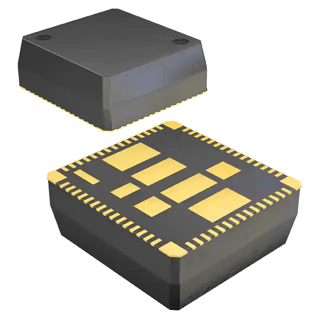
LMZ31530 30-A Power Module With 3-V to 14.5-V Input
in QFN Package
1 Features
3 Description
•
The LMZ31530 power module is an easy-to-use
integrated power solution that combines a 30-A
DC/DC converter with power MOSFETs, a shielded
inductor, and passives into a low profile, QFN
package. This total power solution allows as few as
three external components and eliminates the loop
compensation and magnetics part selection process.
1
•
•
•
•
•
•
•
•
•
•
•
•
•
•
•
•
Complete Integrated Power Solution;
Smaller than a Discrete Design
15 mm × 16 mm × 5.8 mm Package Size
- Pin Compatible with LMZ31520
Ultra-Fast Load Step Response
Efficiencies Up To 96%
Wide-Output Voltage Adjust
0.6 V to 3.6 V, with 1% Reference Accuracy
Optional Split Power Rails Allows
Input Voltage Down to 3 V
Selectable Switching Frequency;
(300 kHz to 850 kHz)
Selectable Slow-Start
Adjustable Over Current Limit
Power Good Output
Output Voltage Sequencing
Over Temperature Protection
Pre-bias Output Start-up
Operating Temperature Range: –40°C to 85°C
Enhanced Thermal Performance: 8.6°C/W
Meets EN55022 Class A Emissions
- Integrated Shielded Inductor
Create a Custom Design Using the LMZ31530
With the WEBENCH® Power Designer
2 Applications
•
•
•
Broadband and Communications Infrastructure
DSP and FPGA Point of Load Applications
High Density Power Systems
The 15 × 16 × 5.8 mm, QFN package is easy to
solder onto a printed circuit board and allows a
compact point-of-load design. Achieves greater than
95% efficiency, has ultra-fast load step response and
excellent power dissipation capability with a thermal
impedance of 8.6°C/W. The LMZ31530 offers the
flexibility and the feature-set of a discrete point-ofload design and is ideal for powering a wide range of
ICs and systems. Advanced packaging technology
affords a robust and reliable power solution
compatible with standard QFN mounting and testing
techniques.
Simplified Application
VIN
CI
PVIN
VIN
V5V
LMZ31530
SENSE+
VOUT
INH
ILIM
FREQ_SEL VADJ
PWRGD
AGND
SS_SEL
VOUT
CO
RSET
PGND
Efficiency
100
95
90
Efficiency (%)
85
80
75
Vout = 1.8 V
Fsw = 500 kHz
70
65
PVIN = 3.3 V, VIN = 5 V
60
PVIN = VIN = 5 V
55
PVIN = VIN = 12 V
50
0
5
10
15
20
Output Current (A)
25
30
C001
1
An IMPORTANT NOTICE at the end of this data sheet addresses availability, warranty, changes, use in safety-critical applications,
intellectual property matters and other important disclaimers. PRODUCTION DATA.
�LMZ31530
SLVSBC7E – OCTOBER 2013 – REVISED SEPTEMBER 2018
www.ti.com
4 Specifications
Absolute Maximum Ratings (1)
4.1
over operating temperature range (unless otherwise noted)
VALUE
Input Voltage
Output Voltage
UNIT
MIN
MAX
VIN, PVIN
–0.3
20
V
INH, VADJ, PWRGD, PWRGD_PU, ILIM, FREQ_SEL,
SS_SEL, V5V
–0.3
7
V
PH
–1
25
V
PH 10ns Transient
–2
27
–0.3
6
V
±200
mV
VOUT
VDIFF (GND to exposed thermal
pad)
Operating Junction Temperature
–40
125 (2)
°C
Storage Temperature
–55
150
°C
Peak Reflow Case Temperature
(3)
245
(4)
Maximum Number of Reflows Allowed (3)
3 (4)
Mechanical Shock
Mil-STD-883D, Method 2002.3, 1 msec, 1/2 sine, mounted
250
Mechanical Vibration
Mil-STD-883D, Method 2007.2, 20-2000Hz
20
(1)
(2)
(3)
(4)
°C
G
Stresses beyond those listed under absolute maximum ratings may cause permanent damage to the device. These are stress ratings
only, and functional operation of the device at these or any other conditions beyond those indicated under recommended operating
conditions is not implied. Exposure to absolute-maximum-rated conditions for extended periods may affect device reliability.
See the temperature derating curves in the Typical Characteristics section for thermal information.
For soldering specifications, refer to the Soldering Requirements for BQFN Packages application note.
Devices with a date code prior to week 14 2018 (1814) have a peak reflow case temperature of 240°C with a maximum of one reflow
4.2 Recommended Operating Conditions
over operating free-air temperature range (unless otherwise noted)
MIN
MAX
UNIT
14.5
V
14.5
V
PVIN
Input Switching Voltage
VIN
Input Bias Voltage
VOUT
Output Voltage
0.6
3.6
V
fSW
Switching Frequency
300
850
kHz
2
4.5
Submit Documentation Feedback
Copyright © 2013–2018, Texas Instruments Incorporated
Product Folder Links: LMZ31530
�LMZ31530
www.ti.com
SLVSBC7E – OCTOBER 2013 – REVISED SEPTEMBER 2018
4.3 Thermal Information
LMZ31530
THERMAL METRIC (1)
RLG
UNIT
72 PINS
θJA
Junction-to-ambient thermal resistance (2)
Natural Convection
8.6
°C/W
(3)
100 LFM
θJA(100LFM)
Junction-to-ambient thermal resistance
7.8
°C/W
ψJT
Junction-to-top characterization parameter (4)
1.6
°C/W
ψJB
Junction-to-board characterization parameter (5)
4.2
°C/W
(1)
For more information about traditional and new thermal metrics, see the ISemiconductor and IC Package Thermal Metrics application
report.
The junction-to-ambient thermal resistance, θJA, applies to devices soldered directly to a 100 mm x 100 mm, 6-layer PCB with 1 oz.
copper and natural convection cooling. Additional airflow reduces θJA.
The junction-to-ambient thermal resistance, θJA, applies to devices soldered directly to a 100 mm x 100 mm, 6-layer PCB with 1 oz.
copper and 100 LFM forced air cooling. Additional airflow reduces θJA.
The junction-to-top characterization parameter, ψJT, estimates the junction temperature, TJ, of a device in a real system, using a
procedure described in JESD51-2A (sections 6 and 7). TJ = ψJT * Pdis + TT; where Pdis is the power dissipated in the device and TT is
the temperature of the top of the device.
The junction-to-board characterization parameter, ψJB, estimates the junction temperature, TJ, of a device in a real system, using a
procedure described in JESD51-2A (sections 6 and 7). TJ = ψJB * Pdis + TB; where Pdis is the power dissipated in the device and TB is
the temperature of the board 1mm from the device.
(2)
(3)
(4)
(5)
4.4 Package Specifications
LMZ31530
UNIT
Weight
Flammability
MTBF Calculated reliability
4.96 grams
Meets UL 94 V-O
Per Bellcore TR-332, 50% stress, TA = 40°C, ground benign
26.5 MHrs
4.5 Electrical Characteristics
TA = -40°C to 85°C, PVIN = VIN = 12 V, VOUT = 1.8 V, IOUT = 30 A
CIN = 2 × 22 µF ceramic and 330 µF bulk, COUT = 4 × 100 µF ceramic (unless otherwise noted)
PARAMETER
IOUT
Output current
VIN
Input bias voltage range
PVIN
Input switching voltage range
UVLO
VIN Undervoltage lockout
VOUT(adj)
Output voltage adjust range
TEST CONDITIONS
MIN
TYP
A
Over IOUT range
4.5
14.5
V
Over IOUT range
3 (1)
14.5
V
VIN Increasing
4.0
4.33
V
3.6
V
Hysteresis
4.2
0.25
Over IOUT range
Temperature variation
-40°C ≤ TA ≤ +85°C
Load regulation
Over IOUT range
Total output voltage variation
Includes set-point, load, and temperature variation
Line regulation
(1)
(2)
UNIT
30
0.6
Set-point voltage tolerance
VOUT
MAX
0
±1.0%
(2)
±2.0%
(2)
±0.25%
+0.4%
PVIN ±10%
±0.1%
Over PVIN range
±0.7%
The minimum PVIN voltage is 3.0V or (VOUT+ 1.1V), whichever is greater. See VIN and PVIN Input Voltage for more details.
The stated limit of the set-point voltage tolerance includes the tolerance of both the internal voltage reference and the internal
adjustment resistor. The overall output voltage tolerance will be affected by the tolerance of the external RSET resistor.
Submit Documentation Feedback
Copyright © 2013–2018, Texas Instruments Incorporated
Product Folder Links: LMZ31530
3
�LMZ31530
SLVSBC7E – OCTOBER 2013 – REVISED SEPTEMBER 2018
www.ti.com
Electrical Characteristics (continued)
TA = -40°C to 85°C, PVIN = VIN = 12 V, VOUT = 1.8 V, IOUT = 30 A
CIN = 2 × 22 µF ceramic and 330 µF bulk, COUT = 4 × 100 µF ceramic (unless otherwise noted)
PARAMETER
TEST CONDITIONS
PVIN = VIN = 12 V
IO = 15 A
Efficiency
η
PVIN = VIN = 5 V
IO = 15 A
MIN
94
VOUT = 1.8 V, fSW = 500kHz
92
VOUT = 1.2 V, fSW = 500kHz
88
VOUT = 0.9 V, fSW = 500kHz
86
VOUT = 0.6 V, fSW = 500kHz
82
VOUT = 3.3 V, fSW = 500kHz
96
VOUT = 1.8 V, fSW = 500kHz
94
VOUT = 1.2 V, fSW = 500kHz
91
VOUT = 0.9 V, fSW = 500kHz
88
VOUT = 0.6 V, fSW = 500kHz
Output voltage ripple
ILIM
VINH
Inhibit Control
IIN(stby)
VIN standby current
2.5 A/µs load step from 25 to 75%
IOUT(max)
Recovery time
VOUT over/undershoot
V
INH pin to AGND
FREQ_SEL pin OPEN, IOUT = 10 A
fSEL
Frequency Select (4)
(4)
(5)
(6)
4
mV
0.6
Switching frequency
(3)
30
-0.3
fSW
External output capacitance
µs
Inhibit Low Voltage
I(PWRGD) = 2 mA
COUT
A
30
Open (3)
PWRGD Low Voltage
External input capacitance
VOUT
40
1.8
VOUT falling
CIN
%
Inhibit High Voltage
PWRGD Thresholds
Thermal Shutdown
UNIT
%
1%
VOUT rising
Power Good
MAX
85
20 MHz bandwith
Current limit threshold
Transient response
TYP
VOUT = 3.3 V, fSW = 500kHz
V
VIN = 5 V
0.5
0.7
mA
VIN = 12 V
1.2
1.5
mA
Good
95
Fault
115
Fault
90
Good
110
470
%
0.2
0.3
V
520
570
kHz
66 kΩ resistor between FREQ_SEL pin and PGND
300
kHz
FREQ_SEL pin connected to V5V (pin 61)
850
kHz
145
°C
10
°C
Thermal shutdown
Thermal shutdown hysteresis
Ceramic
44
(5)
Non-ceramic
94
µF
330
100
(6)
400
5000
µF
This pin has an internal pull-up. If this pin is left open circuit, the device operates when a valid input voltage is applied. A small, lowleakage (


 工商网监
湘ICP备2023018690号
工商网监
湘ICP备2023018690号
