LP339
LP339 Ultra-Low Power Quad Comparator
Literature Number: SNOSBE0A
�LP339
Ultra-Low Power Quad Comparator
General Description
The LP339 consists of four independent voltage comparators designed specifically to operate from a single power
supply and draw typically 60 µA of power supply drain current over a wide range of power supply voltages. Operation
from split supplies is also possible and the ultra-low power
supply drain current is independent of the power supply voltage. These comparators also feature a common-mode
range which includes ground, even when operated from a
single supply.
Applications
include
limit
comparators,
simple
analog-to-digital converters, pulse, square and time delay
generators; VCO’s; multivibrators; high voltage logic gates.
The LP339 was specifically designed to interface with the
CMOS logic family. The ultra-low supply current makes the
LP339 valuable in battery powered applications.
n
n
n
n
Single supply operation
Sensing at ground
Compatible with CMOS logic family
Pin-out identical to LM339
Features
n Ultra-low power supply current drain
(60 µA) — independent of the supply voltage
(75 µW/comparator at +5 VDC)
n Low input biasing current: 3 nA
n Low input offset current: ± 0.5 nA
n Low input offset voltage: ± 2 mV
n Input common-mode voltage includes ground
n Output voltage compatible with MOS and CMOS logic
n High output sink current capability (30 mA at VO =2 VDC)
n Supply Input protected against reverse voltages
Advantages
n Ultra-low power supply drain suitable for battery
applications
Schematic and Connection Diagrams
DS005226-2
DS005226-1
Typical Applications
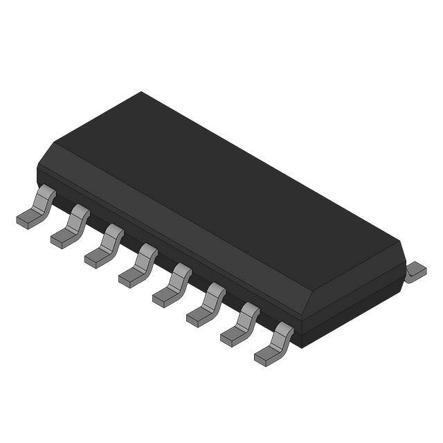
Order Number LP339M for S.O. Package
See NS Package Number M14A
Order Number LP339N for Dual-In-Line Package
See NS Package Number N14A
(V+ = 5.0 VDC)
Basic Comparator
Driving CMOS
DS005226-3
DS005226-4
© 2000 National Semiconductor Corporation
DS005226
www.national.com
LP339 Ultra-Low Power Quad Comparator
August 2000
�LP339
Absolute Maximum Ratings (Note 1)
Operating Temperature Range
0˚C to +70˚C
Storage Temperature Range
−65˚ to +150˚C
Soldering Information:
Dual-In-Line Package (10 sec.)
+260˚C
S.O. Package:
Vapor Phase (60 sec.)
+215˚C
Infrared (15 sec.)
+220˚C
See AN-450 “Surface Mounting Methods and Their Effect on
Product Reliability” for other methods of soldering surface
mount devices.
If Military/Aerospace specified devices are required,
please contact the National Semiconductor Sales Office/
Distributors for availability and specifications.
Supply Voltage
Differential Input Voltage
Input Voltage
Power Dissipation (Note 2)
Molded DIP
Output Short Circuit to GND (Note 3)
Input Current VIN < −0.3 VDC (Note 4)
36 VDC or ± 18 VDC
± 36 VDC
−0.3 VDC to 36 VDC
570 mW
Continuous
50 mA
Electrical Characteristics
(V+=5 VDC) (Note 5)
Typ
Max
Units
Input Offset Voltage
Parameter
TA =25˚C (Note 10)
Conditions
Min
±2
±5
mVDC
Input Bias Current
IIN(+) or IIN(−) with the
2.5
25
nADC
±5
nADC
V+−1.5
VDC
Output in the Linear Range, TA =25˚C (Note 6)
Input Offset Current
IIN(+)−IIN(−), TA =25˚C
Input Common
TA =25˚C (Note 7)
± 0.5
0
Mode Voltage Range
Supply Current
RL =Infinite on all Comparators, TA =25˚C
60
Voltage Gain
VO = 1 VDC to 11 VDC,
500
V/mV
1.3
µSec
8
µSec
15
30
mADC
0.20
0.70
mADC
100
µADC
RL =15 kΩ, V+ =15 VDC, TA =25˚C
Large Signal
VIN =TTL Logic Swing, VREF =1.4 VDC,
Response Time
VRL =5 VDC, RL =5.1 kΩ, TA =25˚C
Response Time
VRL =5 VDC, RL =5.1 kΩ, TA =25˚C (Note 8)
Output Sink Current
VIN(−)=1 VDC, VIN(+)=0, VO =2 VDC,
TA =25˚C (Note 12)
VO =0.4 VDC
Output Leakage Current
VIN(+)=1 VDC, VIN(−)=0, VO =5 VDC, TA =25˚C
Input Offset Voltage
(Note 10)
0.1
Input Offset Current
IIN(+)−IIN(−)
Input Bias Current
IIN(+) or IIN(−) with Output in Linear Range
Input Common
Single Supply
0
VIN(−)=1 VDC, VIN(+)=0, VO =2 VDC
10
nADC
mVDC
±1
±9
± 15
4
40
nADC
V+−2.0
VDC
nADC
Mode Voltage Range
Output Sink Current
mADC
Output Leakage Current
VIN(+)=1 VDC, VIN(−)=0, VO =30 VDC
1.0
µADC
Differential Input Voltage
All VIN’s≥0 VDC (or V− on split supplies) (Note 9)
36
VDC
Note 1: Absolute Maximum Ratings indicate limits beyond which damage to the device may occur. Operating Ratings indicate conditions for which the device is functional, but do not guarantee specific performance limits.
Note 2: For elevated temperature operation, Tj max is 125˚C for the LP339. θja (junction to ambient) is 175˚C/W for the LP339N and 120˚C/W for the LP339M when
either device is soldered in a printed circuit board in a still air environment. The low bias dissipation and the “ON-OFF” characteristic of the outputs keeps the chip
dissipation very small (PD ≤ 100 mW), provided the output transistors are allowed to saturate.
Note 3: Short circuits from the output to V+ can cause excessive heating and eventual destruction. The maximum output current is approximately 50 mA.
Note 4: This input current will only exist when the voltage at any of the input leads is driven negative. It is due to the collector-base junction of the input PNP transistors becoming forward biased and thereby acting as input clamp diodes. In addition to this diode action, there is also lateral NPN parasitic transistor action on the
IC chip. This transistor action can cause the output voltage of the comparators to go to the V+ voltage level (or to ground for a large input overdrive) for the time duration that an input is driven negative. This is not destructive and normal output states will re-establish when the input voltage, which is negative, again returns to a
value greater than −0.3 VDC (TA =25˚C).
Note 5: These specifications apply for V+ =5VDC and 0˚C≤TA≤70˚ C, unless otherwise stated. The temperature extremes are guaranteed but not 100% production
tested. These parameters are not used to calculate outgoing AQL.
Note 6: The direction of the input current is out of the IC due to the PNP input stage. This current is essentially constant, independent of the state of the output, so
no loading change exists on the reference or the input lines as long as the common-mode range is not exceeded.
Note 7: The input common-mode voltage or either input voltage should not be allowed to go negative by more than 0.3V. The upper end of the common-mode voltage range is V+−1.5V (TA =25˚C), but either or both inputs can go to 30 VDC without damage.
Note 8: The response time specified is for a 100 mV input step with 5 mV overdrive. For larger overdrive signals 1.3 µs can be obtained. See Typical Performance
Characteristics section.
www.national.com
2
�LP339
Electrical Characteristics
(Continued)
Note 9: Positive excursions of input voltage may exceed the power supply level. As long as the other voltage remains within the common-mode range, the comparator will provide a proper output state. The low input voltage state must not be less than −0.3 VDC (or 0.3 VDC below the magnitude of the negative power supply, if
used) at TA =25˚C.
Note 10: At output switch point, VO =1.4V, RS =0Ω with V+ from 5 VDC; and over the full input common-mode range (0 VDC to V+−1.5 VDC).
Note 11: For input signals that exceed V+, only the overdriven comparator is affected. With a 5V supply, VIN should be limited to 25V maximum, and a limiting resistor
should be used on all inputs that might exceed the positive supply.
Note 12: The output sink current is a function of the output voltage. The LP339 has a bi-modal output section which allows it to sink large currents via a Darlington
connection at output voltages greater than approximately 1.5 VDC and sink lower currents below this point. (See typical characteristics section and applications section).
Typical Performance Characteristics
Supply Current
Input Current
Output Sink Current
DS005226-35
Output Sink Current
DS005226-37
DS005226-36
Response Times for
Various Input
Overdrives —
Negative Transition
Response Times for
Various Input
Overdrives —
Positive Transition
DS005226-38
DS005226-39
DS005226-40
3
www.national.com
�LP339
Notice that the output section is configured in a Darlington
connection (ignoring Q3). Therefore, if the output voltage is
held high enough (VO≥1 VDC), Q1 is not saturated and the
output current is limited only by the product of the betas of
Q1, Q2 and I1 (and the 60Ω RSAT of Q2). The LP339 is thus
capable of driving LED’s, relays, etc. in this mode while
maintaining an ultra-low power supply current of typically
60 µA.
If transistor Q3 were omitted, and the output voltage allowed
to drop below about 0.8 VDC, transistor Q1 would saturate
and the output current would drop to zero. The circuit would,
therefore, be unable to “pull” low current loads down to
ground (or the negative supply, if used). Transistor Q3 has
been included to bypass transistor Q1 under these conditions and apply the current I1 directly to the base of Q2. The
output sink current is now approximately I1 times the beta of
Q2 (700 µA at VO =0.4 VDC). The output of the LP339 exhibits a bi-modal characteristic with a smooth transition between modes. (See Output Sink Current graphs in Typical
Performance Characteristics section.)
It is also important to note that in both cases the output is an
uncommitted collector. Therefore, many collectors can be
tied together to provide an output OR’ing function. An output
pull-up resistor can be connected to any available power
supply voltage within the permitted power supply voltage
range and there is no restriction on this voltage due to the
magnitude of the voltage which is applied to the V+ terminal
of the LP339 package.
Application Hints
All pins of any unused comparators should be tied to the
negative supply.
The bias network of the LP339 establishes a drain current
which is independent of the magnitude of the power supply
voltage over the range of from 2 VDC to 30 VDC.
It is usually unnecessary to use a bypass capacitor across
the power supply line.
The differential input voltage may be larger than V+ without
damaging the device. Protection should be provided to prevent the input voltages from going negative more than −0.3
VDC (at 25˚C). An input clamp diode can be used as shown
in the application section.
The output section of the LP339 has two distinct modes of
operation-a Darlington mode and a grounded emitter mode.
This unique drive circuit permits the LP339 to sink 30 mA at
VO =2 VDC (Darlington mode) and 700 µA at VO =0.4 VDC
(grounded emitter mode). Figure 1 is a simplified schematic
diagram of the LP339 output section.
DS005226-11
FIGURE 1.
www.national.com
4
�LP339
Typical Applications
(V+ =15 VDC)
One-Shot Multivibrator
DS005226-13
Time-Delay Generator
DS005226-15
5
www.national.com
�LP339
Typical Applications
(V+ =15 VDC) (Continued)
ORing the Outputs
DS005226-16
Squarewave Oscillator
DS005226-17
www.national.com
6
�LP339
Typical Applications
(V+ =15 VDC) (Continued)
Three Level Audio Peak Indicator
DS005226-19
LED Driver
DS005226-22
Pulse Generator
DS005226-18
7
www.national.com
�LP339
Typical Applications
(V+ =15 VDC) (Continued)
Bi-Stable Multivibrator
DS005226-21
Relay Driver
DS005226-23
Buzzer Driver
Comparator With 60 mA Sink Capability
DS005226-24
DS005226-25
www.national.com
8
�LP339
Typical Applications
(V+ =15 VDC) (Continued)
Non-Inverting Comparator with Hysteresis
Inverting Comparator with Hysteresis
DS005226-26
DS005226-27
Comparing Input Voltages
of Opposite Polarity
Basic Comparator
Output Strobing
DS005226-29
DS005226-30
DS005226-28
Transducer Amplifier
Zero Crossing Detector (Single Power Supply)
DS005226-32
DS005226-31
9
www.national.com
�LP339
Typical Applications
(V+ =15 VDC) (Continued)
Split-Supply Applications
Zero Crossing Detector
Comparator With a Negative Reference
DS005226-34
DS005226-33
www.national.com
10
�LP339
Physical Dimensions
inches (millimeters) unless otherwise noted
S.O. Package (M)
Order Number LP339M or LP339MX
NS Package M14A
Molded Dual-In-Line Package (N)
Order Number LP339N
NS Package Number N14A
11
www.national.com
�LP339 Ultra-Low Power Quad Comparator
Notes
LIFE SUPPORT POLICY
NATIONAL’S PRODUCTS ARE NOT AUTHORIZED FOR USE AS CRITICAL COMPONENTS IN LIFE SUPPORT
DEVICES OR SYSTEMS WITHOUT THE EXPRESS WRITTEN APPROVAL OF THE PRESIDENT AND GENERAL
COUNSEL OF NATIONAL SEMICONDUCTOR CORPORATION. As used herein:
1. Life support devices or systems are devices or
systems which, (a) are intended for surgical implant
into the body, or (b) support or sustain life, and
whose failure to perform when properly used in
accordance with instructions for use provided in the
labeling, can be reasonably expected to result in a
significant injury to the user.
National Semiconductor
Corporation
Americas
Tel: 1-800-272-9959
Fax: 1-800-737-7018
Email: support@nsc.com
www.national.com
National Semiconductor
Europe
Fax: +49 (0) 180-530 85 86
Email: europe.support@nsc.com
Deutsch Tel: +49 (0) 69 9508 6208
English Tel: +44 (0) 870 24 0 2171
Français Tel: +33 (0) 1 41 91 8790
2. A critical component is any component of a life
support device or system whose failure to perform
can be reasonably expected to cause the failure of
the life support device or system, or to affect its
safety or effectiveness.
National Semiconductor
Asia Pacific Customer
Response Group
Tel: 65-2544466
Fax: 65-2504466
Email: ap.support@nsc.com
National Semiconductor
Japan Ltd.
Tel: 81-3-5639-7560
Fax: 81-3-5639-7507
National does not assume any responsibility for use of any circuitry described, no circuit patent licenses are implied and National reserves the right at any time without notice to change said circuitry and specifications.
�IMPORTANT NOTICE
Texas Instruments Incorporated and its subsidiaries (TI) reserve the right to make corrections, modifications, enhancements, improvements,
and other changes to its products and services at any time and to discontinue any product or service without notice. Customers should
obtain the latest relevant information before placing orders and should verify that such information is current and complete. All products are
sold subject to TI’s terms and conditions of sale supplied at the time of order acknowledgment.
TI warrants performance of its hardware products to the specifications applicable at the time of sale in accordance with TI’s standard
warranty. Testing and other quality control techniques are used to the extent TI deems necessary to support this warranty. Except where
mandated by government requirements, testing of all parameters of each product is not necessarily performed.
TI assumes no liability for applications assistance or customer product design. Customers are responsible for their products and
applications using TI components. To minimize the risks associated with customer products and applications, customers should provide
adequate design and operating safeguards.
TI does not warrant or represent that any license, either express or implied, is granted under any TI patent right, copyright, mask work right,
or other TI intellectual property right relating to any combination, machine, or process in which TI products or services are used. Information
published by TI regarding third-party products or services does not constitute a license from TI to use such products or services or a
warranty or endorsement thereof. Use of such information may require a license from a third party under the patents or other intellectual
property of the third party, or a license from TI under the patents or other intellectual property of TI.
Reproduction of TI information in TI data books or data sheets is permissible only if reproduction is without alteration and is accompanied
by all associated warranties, conditions, limitations, and notices. Reproduction of this information with alteration is an unfair and deceptive
business practice. TI is not responsible or liable for such altered documentation. Information of third parties may be subject to additional
restrictions.
Resale of TI products or services with statements different from or beyond the parameters stated by TI for that product or service voids all
express and any implied warranties for the associated TI product or service and is an unfair and deceptive business practice. TI is not
responsible or liable for any such statements.
TI products are not authorized for use in safety-critical applications (such as life support) where a failure of the TI product would reasonably
be expected to cause severe personal injury or death, unless officers of the parties have executed an agreement specifically governing
such use. Buyers represent that they have all necessary expertise in the safety and regulatory ramifications of their applications, and
acknowledge and agree that they are solely responsible for all legal, regulatory and safety-related requirements concerning their products
and any use of TI products in such safety-critical applications, notwithstanding any applications-related information or support that may be
provided by TI. Further, Buyers must fully indemnify TI and its representatives against any damages arising out of the use of TI products in
such safety-critical applications.
TI products are neither designed nor intended for use in military/aerospace applications or environments unless the TI products are
specifically designated by TI as military-grade or "enhanced plastic." Only products designated by TI as military-grade meet military
specifications. Buyers acknowledge and agree that any such use of TI products which TI has not designated as military-grade is solely at
the Buyer's risk, and that they are solely responsible for compliance with all legal and regulatory requirements in connection with such use.
TI products are neither designed nor intended for use in automotive applications or environments unless the specific TI products are
designated by TI as compliant with ISO/TS 16949 requirements. Buyers acknowledge and agree that, if they use any non-designated
products in automotive applications, TI will not be responsible for any failure to meet such requirements.
Following are URLs where you can obtain information on other Texas Instruments products and application solutions:
Products
Applications
Audio
www.ti.com/audio
Communications and Telecom www.ti.com/communications
Amplifiers
amplifier.ti.com
Computers and Peripherals
www.ti.com/computers
Data Converters
dataconverter.ti.com
Consumer Electronics
www.ti.com/consumer-apps
DLP® Products
www.dlp.com
Energy and Lighting
www.ti.com/energy
DSP
dsp.ti.com
Industrial
www.ti.com/industrial
Clocks and Timers
www.ti.com/clocks
Medical
www.ti.com/medical
Interface
interface.ti.com
Security
www.ti.com/security
Logic
logic.ti.com
Space, Avionics and Defense
www.ti.com/space-avionics-defense
Power Mgmt
power.ti.com
Transportation and Automotive www.ti.com/automotive
Microcontrollers
microcontroller.ti.com
Video and Imaging
RFID
www.ti-rfid.com
OMAP Mobile Processors
www.ti.com/omap
Wireless Connectivity
www.ti.com/wirelessconnectivity
TI E2E Community Home Page
www.ti.com/video
e2e.ti.com
Mailing Address: Texas Instruments, Post Office Box 655303, Dallas, Texas 75265
Copyright © 2011, Texas Instruments Incorporated
�


 工商网监
湘ICP备2023018690号
工商网监
湘ICP备2023018690号
