Product
Folder
Sample &
Buy
Support &
Community
Tools &
Software
Technical
Documents
LP3470
SNVS003G – JUNE 1999 – REVISED APRIL 2016
LP3470 Voltage Supervisor With Programmable Delay and 1% Reset Threshold
1 Features
3 Description
•
•
•
The LP3470 device is a micropower voltage
supervisory circuit designed to monitor voltages
within 1% of reset threshold over temperature. It
provides maximum adjustability for power-on-reset
(POR) and supervisory functions.
1
•
•
•
•
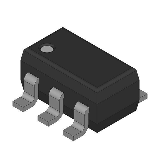
5-Pin SOT-23 Package
Open-Drain Reset Output
Programmable Reset Time-Out Period Using an
External Capacitor
Immune to Short VCC Transients
±1% Reset Threshold Accuracy Over
Temperature
Low Quiescent Current (16 µA typical)
Reset Valid Down to VCC = 0.5 V
2 Applications
•
•
•
•
Critical µP and µC Power Monitoring
Intelligent Instruments
Computers
Portable and Battery-Powered Equipment
The LP3470 asserts a reset signal whenever the VCC
supply voltage falls below a reset threshold. The
reset time-out period is adjustable using an external
capacitor. Reset remains asserted for an interval
(programmed by an external capacitor) after VCC has
risen above the threshold voltage.
For information on available reset threshold voltage
options, see Mechanical, Packaging, and Orderable
Information.
Device Information(1)
PART NUMBER
LP3470
PACKAGE
SOT-23 (5)
BODY SIZE (NOM)
1.60 mm × 2.90 mm
(1) For all available packages, see the Package Option
Addendum at the end of the data sheet.
Basic Operating Circuit
1
An IMPORTANT NOTICE at the end of this data sheet addresses availability, warranty, changes, use in safety-critical applications,
intellectual property matters and other important disclaimers. PRODUCTION DATA.
�LP3470
SNVS003G – JUNE 1999 – REVISED APRIL 2016
www.ti.com
Table of Contents
1
2
3
4
5
6
7
Features ..................................................................
Applications ...........................................................
Description .............................................................
Revision History.....................................................
Pin Configuration and Functions .........................
Specifications.........................................................
1
1
1
2
3
4
6.1
6.2
6.3
6.4
6.5
6.6
4
4
4
4
5
6
Absolute Maximum Ratings .....................................
ESD Ratings..............................................................
Recommended Operating Conditions.......................
Thermal Information ..................................................
Electrical Characteristics...........................................
Typical Characteristics ..............................................
Detailed Description .............................................. 8
7.1 Overview ................................................................... 8
7.2 Functional Block Diagram ......................................... 8
7.3 Feature Description................................................... 8
7.4 Device Functional Modes.......................................... 9
8
Application and Implementation ........................ 10
8.1 Application Information............................................ 10
8.2 Typical Application ................................................. 10
9 Power Supply Recommendations...................... 12
10 Layout................................................................... 12
10.1 Layout Guidelines ................................................. 12
10.2 Layout Example .................................................... 12
11 Device and Documentation Support ................. 13
11.1
11.2
11.3
11.4
Community Resources..........................................
Trademarks ...........................................................
Electrostatic Discharge Caution ............................
Glossary ................................................................
13
13
13
13
12 Mechanical, Packaging, and Orderable
Information ........................................................... 13
4 Revision History
NOTE: Page numbers for previous revisions may differ from page numbers in the current version.
Changes from Revision F (March 2013) to Revision G
Page
•
Added ESD Ratings table, Feature Description section, Device Functional Modes, Application and Implementation
section, Power Supply Recommendations section, Layout section, Device and Documentation Support section, and
Mechanical, Packaging, and Orderable Information section .................................................................................................. 1
•
Moved Operating temperature parameters from Absolute Maximum Ratings to Recommended Operating Conditions....... 4
Changes from Revision E (September 2009) to Revision F
•
2
Page
Changed layout of National Data Sheet to TI format ............................................................................................................. 1
Submit Documentation Feedback
Copyright © 1999–2016, Texas Instruments Incorporated
Product Folder Links: LP3470
�LP3470
www.ti.com
SNVS003G – JUNE 1999 – REVISED APRIL 2016
5 Pin Configuration and Functions
DBV Package
5-Pin SOT-23
Top View
SRT
1
GND
2
VCC1
3
5
Reset
4
VCC
Pin Functions
PIN
NO.
NAME
I/O
DESCRIPTION
1
SRT
O
Set reset time-out. Connect a capacitor between this pin and ground to select the reset time-out period (tRP).
tRP = 2000 × C1 (C1 in µF and tRP in ms). If no capacitor is connected, leave this pin floating.
2
GND
—
Ground pin.
3
VCC1
I
Always connect to pin VCC (Pin 4).
4
VCC
I
Supply voltage, and reset threshold monitor input.
5
Reset
O
Open-drain, active-low reset output. Connect to an external pullup resistor. Reset changes from high to low
whenever the monitored voltage (VCC) drops below the reset threshold voltage (VRTH). Once VCC exceeds
VRTH, Reset remains low for the reset time-out period (tRP) and then goes high.
Submit Documentation Feedback
Copyright © 1999–2016, Texas Instruments Incorporated
Product Folder Links: LP3470
3
�LP3470
SNVS003G – JUNE 1999 – REVISED APRIL 2016
www.ti.com
6 Specifications
6.1 Absolute Maximum Ratings
over operating free-air temperature range (unless otherwise noted) (1) (2)
MIN
MAX
UNIT
VCC voltage
–0.3
6
V
Reset voltage
–0.3
6
V
Output current (Reset)
10
mA
Power dissipation (TA = 25°C) (3)
300
mW
Lead temperature (soldering, 5 sec)
260
°C
Junction temperature, TJMAX
125
°C
150
°C
Storage temperature, Tstg
(1)
(2)
(3)
–65
Stresses beyond those listed under Absolute Maximum Ratings may cause permanent damage to the device. These are stress ratings
only, which do not imply functional operation of the device at these or any other conditions beyond those indicated under Recommended
Operating Conditions. Exposure to absolute-maximum-rated conditions for extended periods may affect device reliability.
If Military/Aerospace specified devices are required, please contact the Texas Instruments Sales Office/Distributors for availability and
specifications.
The maximum power dissipation must be derated at elevated temperatures and is dictated by TJmax (maximum junction temperature),
θJA (junction to ambient thermal resistance), and TA (ambient temperature). The maximum allowable power dissipation at any
temperature is PDmax = (TJmax − TA)/ θJA or the number given in the Absolute Maximum Ratings, whichever is lower.
6.2 ESD Ratings
VALUE
V(ESD)
(1)
(2)
Electrostatic discharge
Human-body model (HBM), per ANSI/ESDA/JEDEC JS-001
(1)
UNIT
±2000
Charged-device model (CDM), per JEDEC specification JESD22-C101 (2)
V
±200
JEDEC document JEP155 states that 500-V HBM allows safe manufacturing with a standard ESD control process.
JEDEC document JEP157 states that 250-V CDM allows safe manufacturing with a standard ESD control process.
6.3 Recommended Operating Conditions
over operating free-air temperature range (unless otherwise noted)
MIN
VCC
Operating voltage
TA
Operating temperature
NOM
MAX
0.5
5.5
LP3470
–20
85
LP3470I
–40
85
UNIT
V
°C
6.4 Thermal Information
LP3470
THERMAL METRIC (1)
DBV (SOT-23)
UNIT
5 PINS
RθJA
Junction-to-ambient thermal resistance
171
°C/W
RθJC(top)
Junction-to-case (top) thermal resistance
124.8
°C/W
RθJB
Junction-to-board thermal resistance
30.9
°C/W
ψJT
Junction-to-top characterization parameter
17.9
°C/W
ψJB
Junction-to-board characterization parameter
30.4
°C/W
RθJC(bot)
Junction-to-case (bottom) thermal resistance
—
°C/W
(1)
4
For more information about traditional and new thermal metrics, see the Semiconductor and IC Package Thermal Metrics application
report, SPRA953.
Submit Documentation Feedback
Copyright © 1999–2016, Texas Instruments Incorporated
Product Folder Links: LP3470
�LP3470
www.ti.com
SNVS003G – JUNE 1999 – REVISED APRIL 2016
6.5 Electrical Characteristics
Limits and typical numbers are for TJ = 25°C, and VCC = 2.4 V to 5 V (unless otherwise noted)
PARAMETER
VCC
Operating voltage
ICC
VCC supply current
TEST CONDITIONS
TJ = –20°C to 85°C
VCC = 4.5 V
Reset threshold voltage
TJ = 25°C
LP3470I
TJ = –40°C to 85°C
VCC to reset delay
VCC falling at 1 mV/µs
tRP
Reset time-out period (4)
C1 = 1 nF
External pullup resistor
ILEAK
Reset output leakage current
(1)
(2)
(3)
(4)
0.99 × VRTH
VRTH
0.99 × VRTH
VRTH
0.985 × VRTH
TJ = –20°C to 85°C
1.01 × VRTH
65
100
TJ = –20°C to 85°C
300
TJ = 25°C
TJ = –20°C to 85°C
2
1
3.5
VCC = 0.5 V, IOL = 30 µA, TJ = –20°C to 85°C
0.1
VCC = 1 V, IOL = 100 µA, TJ = –20°C to 85°C
0.1
VCC =VRTH − 100 mV, IOL = 4 mA,
TJ = –20°C to 85°C
0.4
0.68
TJ = 25°C
TJ = –20°C to 85°C
V
µA
V
1.015 × VRTH
15
TJ = 25°C
UNIT
1.01 × VRTH
35
tPD
R1
5.5
30
TJ = 25°C
Hysteresis voltage (3)
Reset output voltage low
MAX (1)
16
TJ = –20°C to 85°C
VHYST
VOL
TYP (2)
0.5
TJ = 25°C
LP3470
VRTH
MIN (1)
20
68
0.15
1
6
mV
µs
ms
V
kΩ
µA
Minimum and maximum limits in standard typeface are 100% production tested at 25°C. Minimum and maximum limits in full operating
temperature range are ensured through correlation using Statistical Quality Control (SQC) methods. The limits are used to calculate TI's
Average Outgoing Quality Level (AOQL).
Typical numbers are at 25°C and represent the most likely parametric norm.
VHYST affects the relation between VCC and Reset as shown in the timing diagram.
tRP is programmable by varying the value of the external capacitor (C1) connected to pin SRT. The equation is: tRP = 2000 × C1 (C1 in
µF and tRP in ms).
Submit Documentation Feedback
Copyright © 1999–2016, Texas Instruments Incorporated
Product Folder Links: LP3470
5
�LP3470
SNVS003G – JUNE 1999 – REVISED APRIL 2016
www.ti.com
6.6 Typical Characteristics
at TA = 25°C (unless otherwise noted)
6
Figure 1. ICC vs Temperature
Figure 2. ICC vs VCC
Figure 3. VCC to Reset Delay vs Temperature
Figure 4. Normalized tRP vs Temperature
Figure 5. Normalized VRTH vs Temperature
Figure 6. Transient Rejection
Submit Documentation Feedback
Copyright © 1999–2016, Texas Instruments Incorporated
Product Folder Links: LP3470
�LP3470
www.ti.com
SNVS003G – JUNE 1999 – REVISED APRIL 2016
Typical Characteristics (continued)
at TA = 25°C (unless otherwise noted)
Figure 8. VHYST vs Temperature
Figure 7. VHYST vs VRTH
Submit Documentation Feedback
Copyright © 1999–2016, Texas Instruments Incorporated
Product Folder Links: LP3470
7
�LP3470
SNVS003G – JUNE 1999 – REVISED APRIL 2016
www.ti.com
7 Detailed Description
7.1 Overview
The LP3470 micropower voltage supervisory circuit provides a simple solution to monitor the power supplies in
microprocessor and digital systems and provides a reset controlled by the factory-programmed reset threshold
on the VCC supply voltage pin. When the voltage declines below the reset threshold, the reset signal is asserted
and remains asserted for an interval programmed by an external capacitor after VCC has risen above the
threshold voltage. The reset threshold options are 2.63 V, 2.93 V, 3.08 V, 3.65 V, 4 V, 4.38 V, 4.63 V.
7.2 Functional Block Diagram
SRT
LP3470
VCC
VCC1
VREF
Reset
RA
QA
+
_
DELAY
RB
GND
Copyright © 2016, Texas Instruments Incorporated
7.3 Feature Description
7.3.1 Reset Time-Out Period
The reset time-out period (tRP) is programmable using an external capacitor (C1) connected to pin SRT of
LP3470. A ceramic chip capacitor rated at or above 10 V is sufficient. The reset time-out period (tRP) can be
calculated using Equation 1.
tRP (ms) = 2000 x C1 (µF)
(1)
For example a C1 of 100 nF will achieve a tRP of 200 ms. If no delay due to tRP is needed in a certain application,
the pin SRT must be left floating.
7.3.2 Reset Output
In applications like microprocessor (µP) systems, errors might occur in system operation during power up, power
down, or brownout conditions. It is imperative to monitor the power supply voltage to prevent these errors from
occurring.
The LP3470 asserts a reset signal whenever the VCC supply voltage is below a threshold (VRTH) voltage. Reset is
ensured to be a logic low for VCC > 0.5 V. Once VCC exceeds the reset threshold, the reset is kept asserted for a
time period (tRP) programmed by an external capacitor (C1); after this interval Reset goes to logic high. If a
brownout condition occurs (monitored voltage falls below the reset threshold minus a small hysteresis), Reset
goes low. When VCC returns above the reset threshold, Reset remains low for a time period tRP before going to
logic high. Figure 9 shows this behavior.
8
Submit Documentation Feedback
Copyright © 1999–2016, Texas Instruments Incorporated
Product Folder Links: LP3470
�LP3470
www.ti.com
SNVS003G – JUNE 1999 – REVISED APRIL 2016
Feature Description (continued)
Figure 9. Reset Output Timing Diagram
7.3.3 Pullup Resistor Selection
The Reset output structure of the LP3470 is a simple open-drain N-channel MOSFET switch. A pullup resistor
(R1) must be connected to VCC.
R1 must be large enough to limit the current through the output MOSFET (Q1) below 10 mA. A resistor value of
more than 680 Ω ensures this. R1 must also be small enough to ensure a logic high while supplying all the
leakage current through the Reset pin. A resistor value of less than 68 kΩ satisfies this condition. A typical pullup
resistor value of 20 kΩ is sufficient in most applications.
7.3.4 Negative-Going VCC Transients
The LP3470 is relatively immune to short duration negative-going VCC transients (glitches). The Typical
Characteristics show the maximum transient duration versus negative transient amplitude (see Figure 6), for
which reset pulses are not generated. This graph shows the maximum pulse width a negative-going VCC
transient may typically have without causing a reset pulse to be issued. As the transient amplitude increases (in
other words, goes farther below the reset threshold), the maximum allowable pulse width decreases. A 0.1-µF
bypass capacitor mounted close to VCC provides additional transient immunity.
7.4 Device Functional Modes
7.4.1 Reset Output Low
When the VCC supply voltage is below a threshold (VRTH) voltage minus a hysteresis (VHYST) voltage, the Reset
pin will output logic low. Reset is ensured to be a logic low for VCC > 0.5 V.
7.4.2 Reset Output High
When the VCC supply voltage exceeds the reset threshold, the Reset is kept asserted for a time period (tRP)
programmed by an external capacitor (C1); after this interval Reset goes to logic high.
Submit Documentation Feedback
Copyright © 1999–2016, Texas Instruments Incorporated
Product Folder Links: LP3470
9
�LP3470
SNVS003G – JUNE 1999 – REVISED APRIL 2016
www.ti.com
8 Application and Implementation
NOTE
Information in the following applications sections is not part of the TI component
specification, and TI does not warrant its accuracy or completeness. TI’s customers are
responsible for determining suitability of components for their purposes. Customers should
validate and test their design implementation to confirm system functionality.
8.1 Application Information
The LP3470 is a micropower CMOS voltage supervisor that is ideal for use in battery-powered microprocessor
and other digital systems. It is small in size and provides maximum adjustability for power-on-reset (POR) and
supervisory functions, making it a good solution in a variety of applications. The LP3470 is available in six
standard reset threshold voltage options, and the reset time-out period is adjustable using an external capacitor
providing maximum flexibility in any application. This device can ensure system reliability and ensures that a
connected microprocessor will operate only when a minimum Vin supply is satisfied.
8.2 Typical Application
The LP3470 can be used as a simple supervisor circuit to monitor the input supply to a microprocessor as shown
in Figure 10.
Figure 10. Power-On Reset Circuit
8.2.1 Design Requirements
For this design example, use the parameters listed in Table 1 as the input parameters.
Table 1. Design Parameters
DESIGN PARAMETER
10
EXAMPLE VALUE
Input supply voltage
0.5 to 5.5 V
Reset threshold voltage
2.63 V, 2.93 V, 3.08 V, 3.65 V, 4 V, 4.38 V, 4.63 V
External pullup resistor
0.68 to 68 kΩ
External reset time-out period capacitor
C1 = 1 nF
Reset time-out period
2 ms
Submit Documentation Feedback
Copyright © 1999–2016, Texas Instruments Incorporated
Product Folder Links: LP3470
�LP3470
www.ti.com
SNVS003G – JUNE 1999 – REVISED APRIL 2016
8.2.2 Detailed Design Procedure
The minimum application circuit requires the LP3470 Power-On Reset Circuit IC and a pullup resistor connecting
the reset pin to VCC. The reset delay can be programmed with an additional capacitor connected from the SRT
pin to GND. See Reset Time-Out Period and Pullup Resistor Selection for information on choosing specific
values for components.
8.2.3 Application Curves
Two capacitor values for CD (0.1 µF and 1 µF) are used as examples to show the programmability of the output
time delay as shown in Figure 11 and Figure 12.
Figure 11. 0.1-µF Capacitor Programmed Delay
Figure 12. 1-µF Capacitor Programmed Delay
Submit Documentation Feedback
Copyright © 1999–2016, Texas Instruments Incorporated
Product Folder Links: LP3470
11
�LP3470
SNVS003G – JUNE 1999 – REVISED APRIL 2016
www.ti.com
9 Power Supply Recommendations
The input of the LP3470 is designed to handle up to the supply voltage absolute maximum rating of 6 V. If the
input supply is susceptible to any large transients above the maximum rating, then take extra precautions. An
input capacitor is optional but not required to help avoid false reset output triggers due to noise.
10 Layout
10.1 Layout Guidelines
•
•
Place components as close as possible to the IC
Keep traces short between the IC and the C1 capacitor to ensure the timing delay is as accurate as possible.
10.2 Layout Example
Figure 13 shows a layout example.
Figure 13. LP3470 Layout Example
12
Submit Documentation Feedback
Copyright © 1999–2016, Texas Instruments Incorporated
Product Folder Links: LP3470
�LP3470
www.ti.com
SNVS003G – JUNE 1999 – REVISED APRIL 2016
11 Device and Documentation Support
11.1 Community Resources
The following links connect to TI community resources. Linked contents are provided "AS IS" by the respective
contributors. They do not constitute TI specifications and do not necessarily reflect TI's views; see TI's Terms of
Use.
TI E2E™ Online Community TI's Engineer-to-Engineer (E2E) Community. Created to foster collaboration
among engineers. At e2e.ti.com, you can ask questions, share knowledge, explore ideas and help
solve problems with fellow engineers.
Design Support TI's Design Support Quickly find helpful E2E forums along with design support tools and
contact information for technical support.
11.2 Trademarks
E2E is a trademark of Texas Instruments.
All other trademarks are the property of their respective owners.
11.3 Electrostatic Discharge Caution
These devices have limited built-in ESD protection. The leads should be shorted together or the device placed in conductive foam
during storage or handling to prevent electrostatic damage to the MOS gates.
11.4 Glossary
SLYZ022 — TI Glossary.
This glossary lists and explains terms, acronyms, and definitions.
12 Mechanical, Packaging, and Orderable Information
The following pages include mechanical, packaging, and orderable information. This information is the most
current data available for the designated devices. This data is subject to change without notice and revision of
this document. For browser-based versions of this data sheet, refer to the left-hand navigation.
Submit Documentation Feedback
Copyright © 1999–2016, Texas Instruments Incorporated
Product Folder Links: LP3470
13
�PACKAGE OPTION ADDENDUM
www.ti.com
8-Jul-2022
PACKAGING INFORMATION
Orderable Device
Status
(1)
Package Type Package Pins Package
Drawing
Qty
Eco Plan
(2)
Lead finish/
Ball material
MSL Peak Temp
Op Temp (°C)
Device Marking
(3)
(4/5)
(6)
LP3470IM5-2.63/NOPB
NRND
SOT-23
DBV
5
1000
RoHS & Green
SN
Level-1-260C-UNLIM
LP3470IM5-2.75/NOPB
NRND
SOT-23
DBV
5
1000
RoHS & Green
SN
Level-1-260C-UNLIM
D38C
LP3470IM5-2.83/NOPB
NRND
SOT-23
DBV
5
1000
RoHS & Green
SN
Level-1-260C-UNLIM
D39C
LP3470IM5-2.93
NRND
SOT-23
DBV
5
1000
Non-RoHS
& Green
Call TI
Level-1-260C-UNLIM
-40 to 85
D26C
LP3470IM5-2.93/NOPB
NRND
SOT-23
DBV
5
1000
RoHS & Green
SN
Level-1-260C-UNLIM
-40 to 85
D26C
LP3470IM5-3.08
NRND
SOT-23
DBV
5
1000
Non-RoHS
& Green
Call TI
Level-1-260C-UNLIM
-40 to 85
D28C
LP3470IM5-3.08/NOPB
NRND
SOT-23
DBV
5
1000
RoHS & Green
SN
Level-1-260C-UNLIM
-40 to 85
D28C
LP3470IM5-3.65/NOPB
NRND
SOT-23
DBV
5
1000
RoHS & Green
SN
Level-1-260C-UNLIM
-40 to 85
D37C
LP3470IM5-4.00
NRND
SOT-23
DBV
5
1000
Non-RoHS
& Green
Call TI
Level-1-260C-UNLIM
-40 to 85
D29C
LP3470IM5-4.00/NOPB
NRND
SOT-23
DBV
5
1000
RoHS & Green
SN
Level-1-260C-UNLIM
-40 to 85
D29C
LP3470IM5-4.38
NRND
SOT-23
DBV
5
1000
Non-RoHS
& Green
Call TI
Level-1-260C-UNLIM
-40 to 85
D30C
LP3470IM5-4.38/NOPB
NRND
SOT-23
DBV
5
1000
RoHS & Green
SN
Level-1-260C-UNLIM
-40 to 85
D30C
LP3470IM5-4.63
NRND
SOT-23
DBV
5
1000
Non-RoHS
& Green
Call TI
Level-1-260C-UNLIM
-40 to 85
D31C
LP3470IM5-4.63/NOPB
NRND
SOT-23
DBV
5
1000
RoHS & Green
SN
Level-1-260C-UNLIM
-40 to 85
D31C
LP3470IM5-4.8/NOPB
NRND
SOT-23
DBV
5
1000
RoHS & Green
SN
Level-1-260C-UNLIM
LP3470IM5X-2.63/NOPB
NRND
SOT-23
DBV
5
3000
RoHS & Green
SN
Level-1-260C-UNLIM
LP3470IM5X-2.83/NOPB
NRND
SOT-23
DBV
5
3000
RoHS & Green
SN
Level-1-260C-UNLIM
LP3470IM5X-2.93/NOPB
NRND
SOT-23
DBV
5
3000
RoHS & Green
SN
Level-1-260C-UNLIM
-40 to 85
D26C
LP3470IM5X-3.08
NRND
SOT-23
DBV
5
3000
Non-RoHS
& Green
Call TI
Level-1-260C-UNLIM
-40 to 85
D28C
LP3470IM5X-3.08/NOPB
NRND
SOT-23
DBV
5
3000
RoHS & Green
SN
Level-1-260C-UNLIM
-40 to 85
D28C
LP3470IM5X-4.00
NRND
SOT-23
DBV
5
3000
Non-RoHS
& Green
Call TI
Level-1-260C-UNLIM
-40 to 85
D29C
LP3470IM5X-4.00/NOPB
NRND
SOT-23
DBV
5
3000
RoHS & Green
SN
Level-1-260C-UNLIM
-40 to 85
D29C
LP3470IM5X-4.38/NOPB
NRND
SOT-23
DBV
5
3000
RoHS & Green
SN
Level-1-260C-UNLIM
-40 to 85
D30C
LP3470IM5X-4.63/NOPB
NRND
SOT-23
DBV
5
3000
RoHS & Green
SN
Level-1-260C-UNLIM
-40 to 85
D31C
Addendum-Page 1
-40 to 85
D25C
D15C
-40 to 85
D25C
D39C
Samples
�PACKAGE OPTION ADDENDUM
www.ti.com
Orderable Device
8-Jul-2022
Status
(1)
Package Type Package Pins Package
Drawing
Qty
Eco Plan
(2)
Lead finish/
Ball material
MSL Peak Temp
SN
Level-1-260C-UNLIM
Op Temp (°C)
Device Marking
(3)
(4/5)
(6)
LP3470M5-2.63/NOPB
NRND
SOT-23
DBV
5
1000
RoHS & Green
0 to 0
D25B
LP3470M5-2.93/NOPB
NRND
SOT-23
DBV
5
1000
RoHS & Green
SN
LP3470M5-3.08
NRND
SOT-23
DBV
5
1000
Non-RoHS
& Green
Call TI
Level-1-260C-UNLIM
0 to 0
D26B
Level-1-260C-UNLIM
-20 to 85
D28B
LP3470M5-3.08/NOPB
NRND
SOT-23
DBV
5
1000
RoHS & Green
LP3470M5-4.00/NOPB
NRND
SOT-23
DBV
5
1000
RoHS & Green
SN
Level-1-260C-UNLIM
0 to 0
D28B
SN
Level-1-260C-UNLIM
0 to 0
D29B
LP3470M5-4.38/NOPB
NRND
SOT-23
DBV
5
1000
LP3470M5-4.63
NRND
SOT-23
DBV
5
1000
RoHS & Green
SN
Level-1-260C-UNLIM
0 to 0
D30B
Non-RoHS
& Green
Call TI
Level-1-260C-UNLIM
-20 to 85
D31B
LP3470M5-4.63/NOPB
NRND
SOT-23
DBV
5
1000
RoHS & Green
SN
Level-1-260C-UNLIM
0 to 0
D31B
LP3470M5X-2.93/NOPB
NRND
SOT-23
DBV
5
3000
RoHS & Green
SN
Level-1-260C-UNLIM
0 to 0
D26B
LP3470M5X-3.08/NOPB
NRND
SOT-23
DBV
5
3000
RoHS & Green
SN
Level-1-260C-UNLIM
0 to 0
D28B
LP3470M5X-4.00/NOPB
NRND
SOT-23
DBV
5
3000
RoHS & Green
SN
Level-1-260C-UNLIM
0 to 0
D29B
LP3470M5X-4.63/NOPB
NRND
SOT-23
DBV
5
3000
RoHS & Green
SN
Level-1-260C-UNLIM
0 to 0
D31B
(1)
The marketing status values are defined as follows:
ACTIVE: Product device recommended for new designs.
LIFEBUY: TI has announced that the device will be discontinued, and a lifetime-buy period is in effect.
NRND: Not recommended for new designs. Device is in production to support existing customers, but TI does not recommend using this part in a new design.
PREVIEW: Device has been announced but is not in production. Samples may or may not be available.
OBSOLETE: TI has discontinued the production of the device.
(2)
RoHS: TI defines "RoHS" to mean semiconductor products that are compliant with the current EU RoHS requirements for all 10 RoHS substances, including the requirement that RoHS substance
do not exceed 0.1% by weight in homogeneous materials. Where designed to be soldered at high temperatures, "RoHS" products are suitable for use in specified lead-free processes. TI may
reference these types of products as "Pb-Free".
RoHS Exempt: TI defines "RoHS Exempt" to mean products that contain lead but are compliant with EU RoHS pursuant to a specific EU RoHS exemption.
Green: TI defines "Green" to mean the content of Chlorine (Cl) and Bromine (Br) based flame retardants meet JS709B low halogen requirements of


 工商网监
湘ICP备2023018690号
工商网监
湘ICP备2023018690号
