Product
Folder
Order
Now
Support &
Community
Tools &
Software
Technical
Documents
LP5569
SNVSAP8A – JULY 2017 – REVISED SEPTEMBER 2017
LP5569 Nine-Channel I2C RGB LED Driver With Engine Control and Charge Pump
1 Features
3 Description
•
•
The LP5569 device is a programmable, easy-to-use
9-channel I2C LED driver designed to produce lighting
effects for various applications. The LED driver is
equipped with an internal SRAM memory for userprogrammed sequences and three programmable
LED engines, which allow operation without
processor control. Autonomous operation reduces
system power consumption when the processor is put
in sleep mode.
1
•
•
•
•
•
•
Supply Voltage Range: 2.5 V–5.5 V
Nine High-Accuracy Current Sinks
– 25.5 mA Maximum per Channel
– 8-Bit Individual Current Control
– 12-Bit 20-kHz Internal Individual PWM Control
Without Audio Noise
Three Programmable LED Engines
– Independent Illumination Control Without
Active Microcontroller Control
– Synchronization Among Multiple Devices
– Up to 256 Instructions in SRAM Memory for
Storing Sequences of Lighting Patterns
– LP5523- and LP55231-Device-Compatible
Command Set
Flexible Dimming Control
– I2C Dimming Control
– PWM Direct-Input Dimming
– PWM Input Frequency: 100-Hz to 20-kHz
Adaptive High-Efficiency Charge-Pump Control for
Driving High-VF LEDs With Low Battery Voltage
Master Fader Control Allows Dimming of Multiple
LEDs by Writing to Only One Register to Reduce
the I2C Bus Traffic
2-µA Low Standby Current and 10-µA in
Automatic Power-Save Mode When LEDs Are
Inactive
POR, UVLO, and TSD Protection
A high-efficiency charge pump enables the driving of
LEDs with high VF, even with 2.5-V input voltage. The
LP5569 LED driver maintains good efficiency over a
wide operational voltage range by autonomously
selecting the best charge-pump gain based on LED
forward voltage requirements.
The LP5569 device enters power-save mode when
LEDs are not active, lowering idle-current
consumption considerably. A flexible digital interface
allows the connection of up to eight LP5569 devices
with a unique I2C slave address for each device in
the same system, which supports synchronization of
the lighting effects among all devices.
Device Information(1)
PART NUMBER
LP5569
BODY SIZE (NOM)
4.00 mm × 4.00 mm
(1) For all available packages, see the orderable addendum at
the end of the data sheet.
Simplified Schematic
CFLY1
1 μF
2 Applications
LED Lighting, Indicator Lights, and Fun Lights for:
• Smart Speaker
• Smart Home Appliance
• Doorbell
• Electric Lock
• Smoke Detector
• Thermostat
• Set-Top Box
• Smart Router
• Bluetooth® Headset
• Cell Phone
PACKAGE
WQFN (24)
VIN
C1–
2.5 V to 5.5 V
CIN
1 μF
VIN
C1+
CFLY2
1 μF
C2–
C2+
VOUT
COUT
1 μF
PGND
VIN
1.8 V
V1P8
LED0
LED1
µC
SCL
LED2
SDA
LED3
EN/PWM
LED4
CLK
LED5
GPIO/TRIG/INT
LED6
ADDR
LED7
AGND
LED8
Copyright © 2017, Texas Instruments Incorporated
1
An IMPORTANT NOTICE at the end of this data sheet addresses availability, warranty, changes, use in safety-critical applications,
intellectual property matters and other important disclaimers. PRODUCTION DATA.
�LP5569
SNVSAP8A – JULY 2017 – REVISED SEPTEMBER 2017
www.ti.com
Table of Contents
1
2
3
4
5
6
7
Features ..................................................................
Applications ...........................................................
Description .............................................................
Revision History.....................................................
Device Comparison Table.....................................
Pin Configuration and Functions .........................
Specifications.........................................................
1
1
1
2
3
3
5
7.1
7.2
7.3
7.4
7.5
7.6
7.7
7.8
7.9
7.10
5
5
5
5
6
6
7
7
7
Absolute Maximum Ratings ......................................
ESD Ratings..............................................................
Recommended Operating Conditions.......................
Thermal Information ..................................................
Electrical Characteristics...........................................
Charge-Pump Electrical Characteristics ...................
LED Current Sinks Electrical Characteristics............
Logic Interface Characteristics..................................
Timing Requirements (EN/PWM)..............................
Serial-Bus Timing Requirements (SDA, SCL), See
Figure 1......................................................................
7.11 External Clock Timing Requirements (CLK), See
Figure 2......................................................................
7.12 Typical Characteristics ............................................
8
8
8
9
Detailed Description ............................................ 11
8.1
8.2
8.3
8.4
8.5
8.6
9
Overview .................................................................
Functional Block Diagram .......................................
Feature Description.................................................
Device Functional Modes........................................
Programming...........................................................
Register Maps .........................................................
11
12
13
21
23
38
Application and Implementation ........................ 78
9.1 Application Information............................................ 78
9.2 Typical Applications ................................................ 78
10 Power Supply Recommendations ..................... 82
11 Layout................................................................... 83
11.1 Layout Guidelines ................................................. 83
11.2 Layout Example .................................................... 84
12 Device and Documentation Support ................. 85
12.1
12.2
12.3
12.4
12.5
12.6
Device Support ....................................................
Receiving Notification of Documentation Updates
Community Resources..........................................
Trademarks ...........................................................
Electrostatic Discharge Caution ............................
Glossary ................................................................
85
85
85
85
85
85
13 Mechanical, Packaging, and Orderable
Information ........................................................... 85
4 Revision History
Changes from Original (July 2017) to Revision A
•
2
Page
Added typical curves .............................................................................................................................................................. 9
Submit Documentation Feedback
Copyright © 2017, Texas Instruments Incorporated
Product Folder Links: LP5569
�LP5569
www.ti.com
SNVSAP8A – JULY 2017 – REVISED SEPTEMBER 2017
5 Device Comparison Table
PART NUMBER
GROUP
I2C SLAVE ADDRESS
LP5569
0
32h–35h and 40h (see I2C Slave Addressing)
LP5569A
1
42h–45h and 40h (see I2C Slave Addressing)
6 Pin Configuration and Functions
C1±
C2±
VOUT
PGND
ADDR
LED0
24
23
22
21
20
19
RTW Package
24-Pin WQFN With Exposed Thermal Pad
Top View
C2+
1
18
LED1
C1+
2
17
LED2
VIN
3
16
LED3
AGND
4
15
LED4
EN/PWM
5
14
LED5
CLK
6
13
LED6
Thermal
7
8
9
10
11
12
GPIO/TRIG/INT
SDA
SCL
V1P8
LED8
LED7
Pad
Not to scale
Pin Functions
PIN
NAME
NO.
TYPE (1)
DESCRIPTION
ADDR
20
I
I2C slave-address selection pin. See I2C Slave Addressing for more details. This pin
must not be left floating.
AGND
4
G
Analog and digital ground. Connect to PGND, exposed thermal pad, and common
ground plane.
C1–
24
A
Negative pin of charge-pump flying capacitor 1. If charge pump is not used, this pin must
be left floating.
C1+
2
A
Positive pin of charge-pump flying capacitor 1. If charge pump is not used, this pin must
be left floating.
C2–
23
A
Negative pin of charge-pump flying capacitor 2. If charge pump is not used, this pin must
be left floating.
C2+
1
A
Positive pin of charge-pump flying capacitor 2. If charge pump is not used, this pin must
be left floating.
CLK
6
I, OD
EN/PWM
5
I
(1)
Clock input/output. By default this pin is a clock input. If not used, this pin must be
connected to GND or VIN.
Chip enable and PWM input pin.
A: analog pin; G: ground pin; P: power pin; I: input pin; OD: open-drain output pin
Submit Documentation Feedback
Copyright © 2017, Texas Instruments Incorporated
Product Folder Links: LP5569
3
�LP5569
SNVSAP8A – JULY 2017 – REVISED SEPTEMBER 2017
www.ti.com
Pin Functions (continued)
PIN
NAME
NO.
TYPE (1)
DESCRIPTION
General-purpose input or open-drain output, or trigger input or open-drain output, or
interrupt open-drain output. This pin function is configured in the I2C registers. By default
this pin is a general-purpose output (open-drain) and can be left floating if not used.
GPIO/TRIG/INT
7
I, OD
LED0
19
A
LED current sink 0. If not used, this pin can be left floating.
LED1
18
A
LED current sink 1. If not used, this pin can be left floating.
LED2
17
A
LED current sink 2. If not used, this pin can be left floating.
LED3
16
A
LED current sink 3. If not used, this pin can be left floating.
LED4
15
A
LED current sink 4. If not used, this pin can be left floating.
LED5
14
A
LED current sink 5. If not used, this pin can be left floating.
LED6
13
A
LED current sink 6. If not used, this pin can be left floating.
LED7
12
A
LED current sink 7. If not used, this pin can be left floating.
LED8
11
A
LED current sink 8. If not used, this pin can be left floating.
PGND
21
G
Charge-pump power ground. Connect to AGND, exposed thermal pad, and common
ground plane.
SCL
9
I
I2C bus clock line. If not used, this pin must be connected to GND or VIN.
SDA
8
I, OD
I2C bus data line. If not used, this pin must be connected to GND or VIN.
V1P8
10
P
Input power for digital circuitry.
VIN
3
P
Input power, a 1-µF capacitor must be connected between PGND and this pin.
VOUT
22
A
Charge-pump output voltage. If charge pump is used, a 1-µF capacitor must be
connected between PGND and this pin. If charge pump is not used or is used in 1×
mode only, the capacitor can be omitted.
Exposed thermal
pad
—
—
Must be connected to AGND (pin 4), PGND (pin 21), and common ground plane. See
Layout Example. Must be soldered to achieve appropriate power dissipation and
mechanical reliability.
4
Submit Documentation Feedback
Copyright © 2017, Texas Instruments Incorporated
Product Folder Links: LP5569
�LP5569
www.ti.com
SNVSAP8A – JULY 2017 – REVISED SEPTEMBER 2017
7 Specifications
7.1 Absolute Maximum Ratings
over operating ambient temperature range (unless otherwise noted) (1)
MIN
MAX
Voltage on VIN, CLK, ADDR, EN/PWM, GPIO/TRIG/INT, SCL, SDA,
VOUT (2)
–0.3
6
V
Voltage on LED0 to LED8, C1–, C2–, C1+, C2+
−0.3
VVIN + 0.3 V with 6 V max.
V
Voltage on V1P8
−0.3
2
V
Continuous power dissipation
UNIT
Internally limited
Internally limited
Junction temperature, TJ-MAX
–40
125
°C
Storage temperature, Tstg
−65
150
°C
(1)
(2)
Stresses beyond those listed under Absolute Maximum Ratings may cause permanent damage to the device. These are stress ratings
only, which do not imply functional operation of the device at these or any other conditions beyond those indicated under Recommended
Operating Conditions. Exposure to absolute-maximum-rated conditions for extended periods may affect device reliability.
VOUT cannot be forced to a power supply during device shutdown.
7.2 ESD Ratings
VALUE
V(ESD)
(1)
(2)
Electrostatic discharge
Human-body model (HBM), per ANSI/ESDA/JEDEC JS-001 (1)
±2500
Charged-device model (CDM), per JEDEC specification JESD22C101 (2)
±250
UNIT
V
JEDEC document JEP155 states that 500-V HBM allows safe manufacturing with a standard ESD control process.
JEDEC document JEP157 states that 250-V CDM allows safe manufacturing with a standard ESD control process.
7.3 Recommended Operating Conditions
over operating ambient temperature range (unless otherwise noted)
MIN
MAX
2.5
5.5
V
Voltage on LED0 to LED8, C1–, C2–, C1+, C2+, VOUT
0
VVIN
V
Voltage on CLK, ADDR, EN/PWM, GPIO/TRIG/INT, SDA, SCL
0
VVIN
V
1.65
1.95
V
0
160
mA
−40
85
°C
Input voltage on VIN
Input voltage on V1P8
Output current on VOUT
Operating ambient temperature, TA
(1)
(1)
UNIT
In applications where high power dissipation and/or poor PCB cooling status is present, the maximum ambient temperature might
require derating. Maximum ambient temperature (TA-MAX) is dependent on the maximum operating junction temperature (TJ-MAX-OP =
125°C), the maximum power dissipation of the device in the application (PD-MAX), and the junction-to ambient thermal resistance of the
device in the application (RθJA), as given by the equation: TA-MAX = TJ-MAX-OP – (RθJA × PD-MAX).
7.4 Thermal Information
LP5569
THERMAL METRIC (1)
RTW (WQFN)
UNIT
24 PINS
RθJA
Junction-to-ambient thermal resistance
35.8
°C/W
RθJC(top)
Junction-to-case (top) thermal resistance
26.7
°C/W
RθJB
Junction-to-board thermal resistance
13.1
°C/W
ψJT
Junction-to-top characterization parameter
0.4
°C/W
ψJB
Junction-to-board characterization parameter
13.1
°C/W
RθJC(bot)
Junction-to-case (bottom) thermal resistance
4.6
°C/W
(1)
For more information about traditional and new thermal metrics, see Semiconductor and IC Package Thermal Metrics.
Submit Documentation Feedback
Copyright © 2017, Texas Instruments Incorporated
Product Folder Links: LP5569
5
�LP5569
SNVSAP8A – JULY 2017 – REVISED SEPTEMBER 2017
www.ti.com
7.5 Electrical Characteristics
Unless otherwise noted, specifications apply to the LP5569 device in a circuit per the typical application diagram for the single
device with VVIN = 3.6 V, V1P8 = 1.8 V, VEN/PWM = VVIN, CIN = COUT = CFLY1 = CFLY2 = 1 µF. Typical (TYP) values apply for TA =
25°C and minimum (MIN) and maximum (MAX) apply over the operating ambient temperature range (−40°C < TA < 85°C).
PARAMETER
TEST CONDITIONS
MIN
TYP
MAX
0.2
1
VEN/PWM = 3.3 V, chip_en (bit) = 0, external CLK
not running
1
2
VEN/PWM = 3.3 V, chip_en (bit) = 0, external CLK
running
2
4
External CLK running, charge pump and current
sinks disabled
56
70
Charge pump in 1× mode, no load, current
sinks disabled
65
90
Charge pump in 1.5× mode, no load, currentsink outputs disabled
1.8
External CLK running, see Automatic PowerSave Mode
10
15
Internal oscillator running
10
15
VEN/PWM = 0 V, chip_en(bit) = 0
0.2
1
µA
VEN/PWM = 3.3 V, chip_en (bit) = 0, external CLK
not running
0.2
2
µA
VEN/PWM = 3.3 V, chip_en (bit) = 0, external CLK
running
1
4
µA
External CLK running, charge pump and current
sinks disabled
174
190
µA
Charge pump in 1× mode, no load, current
sinks disabled
174
190
µA
Charge pump in 1.5× mode, no load, currentsink- outputs disabled
180
VEN/PWM = 0 V, chip_en (bit) = 0
Standby supply current
IVIN
Normal-mode supply current
Power-save mode supply
current
Standby supply current
IV1P8
Normal-mode supply current
Powersave-mode supply
current
ƒOSC
VUVLO
32-kHz internal oscillator
frequency accuracy
µA
µA
mA
µA
µA
External CLK running
1
5
µA
Internal oscillator running
1
5
µA
TA = 25°C
10-MHz internal oscillator
frequency accuracy
Undervoltage lockout
UNIT
–10%
10%
–7%
7%
VVIN falling
2.2
VVIN rising
2.3
V
7.6 Charge-Pump Electrical Characteristics
PARAMETER
ROUT
Charge-pump output resistance
ƒSW
Switching frequency
ICL
Output current limit
tON
VOUT turnon time
6
Maximum output current
MIN
TYP
MAX
1
Gain = 1.5×, VVIN = 3.7 V
VVIN = 3.7 V, IOUT = 160 mA,
gain = 1.5×
VOUT
IOUT
TEST CONDITIONS
Gain = 1×, VVIN = 4.2 V
Ω
3.5
4.41
4.5
UNIT
4.59
V
1.25
MHz
VOUT = 0 V, VVIN = 3.7 V,
CP_CONFIG = 0xFF
600
mA
IOUT = 0 mA, VIN ≥ 3 V, VOUT >
4.1 V, gain = 1.5×
100
µs
VVIN > 3.1 V, VOUT dropped
10%, gain = 1.5×
200
VIN > 2.5 V, VOUT dropped 10%,
gain = 1.5×
150
Submit Documentation Feedback
mA
Copyright © 2017, Texas Instruments Incorporated
Product Folder Links: LP5569
�LP5569
www.ti.com
SNVSAP8A – JULY 2017 – REVISED SEPTEMBER 2017
7.7 LED Current Sinks Electrical Characteristics
PARAMETER
ILEAKAGE
Leakage current (LED0 to LED8)
IMAX
Maximum sink current
ILED_ACC
Sink current accuracy (1)
Matching
ƒLED
LED switching frequency
(1)
(2)
Saturation voltage
MIN
TYP
24.5
Current set to 17.5 mA. PWM =
100%
(1)
ILED_MATCH
VSAT
TEST CONDITIONS
PWM = 0%, VLED = 5 V
25.5
–4.5%
MAX
µA
26.5
mA
4.5%
Current set to 17.5 mA
1%
2.5%
19.5
(2)
UNIT
1
Output current set to 25.5 mA
90
kHz
110
mV
Output-current accuracy is the difference between the actual value of the output current and the programmed value of this current.
Matching is the maximum difference from the average. For the constant-current outputs on the device (LED0 to LED8), the following are
determined: the maximum output current (MAX), the minimum output current (MIN), and the average output current of all outputs (AVG).
The matching number is calculated: (MAX – MIN) / AVG. The typical specification provided is the most likely norm of the matching figure
for all devices. Note that some manufacturers have different definitions in use.
Saturation voltage is defined as the voltage when the LED current has dropped 10% from the value measured at 1 V.
7.8 Logic Interface Characteristics
PARAMETER
TEST CONDITIONS
MIN
TYP
MAX
UNIT
LOGIC INPUT (EN/PWM, SCL, ADDR)
VIL
Input low level
VIH
Input high level
Ilkg
Input leakage current
0.4
V
1
µA
0.4
V
1.25
VI ≤ VVIN
V
–1
LOGIC OUTPUT (SDA, GPIO/TRIG/INT, CLK)
VIL
Input low level
Pin configured as input
VIH
Input high level
Pin configured as input
Ilkg
Input leakage current
Pin configured as input, VVIN
= 5.5 V, VI ≤ VVIN
VOL
Output low level
IPULLUP = 3 mA
Output leakage current
Pin configured as output, HiZ state
IL
1.25
V
–1
0.2
1
µA
0.5
V
1
µA
7.9 Timing Requirements (EN/PWM)
MIN
2
TYP
MAX
2
3
UNIT
tEN
Enable time, EN/PWM first rising edge until first I C access
tEN_TIMEOUT
EN timeout, EN/PWM = low time while in standby mode (enable
function)
ms
15
ms
tPWM_TIMEOUT
PWM timeout, EN/PWM = low time while in normal mode (PWM
function)
15
ms
PWMres
Resolution for EN/PWM input when configured as PWM, fPWM
=10 kHz
10
bits
Submit Documentation Feedback
Copyright © 2017, Texas Instruments Incorporated
Product Folder Links: LP5569
7
�LP5569
SNVSAP8A – JULY 2017 – REVISED SEPTEMBER 2017
www.ti.com
7.10 Serial-Bus Timing Requirements (SDA, SCL), See Figure 1
I2C fast mode
MIN
MAX
UNIT
0
400
kHz
ƒSCL
Clock frequency
1
Hold time (repeated) START condition
0.6
µs
2
Clock low time
1.3
µs
3
Clock high time
600
ns
4
Setup time for a repeated START condition
600
ns
5
Data hold time
0
ns
6
Data setup time
100
ns
7
Rise time of SDA and SCL
20 + 0.1Cb
300
ns
8
Fall time of SDA and SCL
15 + 0.1Cb
300
ns
9
Setup time for STOP condition
600
10
Bus-free time between a STOP and a START condition
1.3
Cb
Capacitive load for each bus line
10
ns
µs
200
pF
7.11 External Clock Timing Requirements (CLK), See Figure 2
over operating ambient temperature range (unless otherwise noted)
MIN
TYP
MAX
32.7
UNIT
ƒCLK
Clock frequency
tCLKH
High time
6
kHz
µs
tCLKL
Low time
6
µs
tr
Clock rise time, 10% rising edge to 90% rising edge
2
µs
tf
Clock fall time, 90% falling edge to 10% falling edge
2
µs
Figure 1. Timing Parameters
Figure 2. External Clock Signal
8
Submit Documentation Feedback
Copyright © 2017, Texas Instruments Incorporated
Product Folder Links: LP5569
�LP5569
www.ti.com
SNVSAP8A – JULY 2017 – REVISED SEPTEMBER 2017
7.12 Typical Characteristics
Unless otherwise specified: VVIN = 3.6 V, CIN = COUT = 1 μF, C1 = C2 = 1 μF, TA = 25°C. CIN, COUT, C1, C2: Low-ESR surfacemount ceramic capacitors (MLCCs) used in setting electrical characteristics.
0.9
5
0.875
4.75
Charge Pump Voltage (V)
0.85
Efficiency
0.825
0.8
0.775
0.75
0.725
0.7
0.675
VVIN = 3 V
VVIN = 3.3 V
VVIN = 3.6 V
0.65
VVIN = 3.9 V
VVIN = 4.2 V
4.5
4.25
4
3.75
3.5
3.25
3
VVIN = 2.5 V
VVIN = 3 V
VVIN = 3.3 V
2.75
VVIN = 3.6 V
VVIN = 3.9 V
VVIN = 4.2 V
2.5
0.625
0
0.02 0.04 0.06 0.08 0.1 0.12 0.14 0.16 0.18
Load Current (A)
0
0.2
10
20
D004
30
40 50 60 70 80
Load Current (mA)
90 100 110 120
D005
Figure 3. Charge Pump 1.5× Efficiency vs Load Current
Figure 4. Output Voltage of the Charge Pump (1.5×) as a
Function of Load Current at Six Input Voltage Levels
Figure 5. Charge Pump (1×) Start-Up Waveform
Figure 6. Charge Pump (1.5×) Start-Up Waveform
10.2
9.8
Internal CLK
External CLK
9.4
IVIN (PA)
9
8.6
8.2
7.8
7.4
7
2.5
3
3.5
4
VVIN (V)
4.5
5
5.5
D006
Figure 8. Supply Current in Power-Save Mode vs VVIN
Figure 7. Charge Pump (Auto) Start-Up Waveform
Submit Documentation Feedback
Copyright © 2017, Texas Instruments Incorporated
Product Folder Links: LP5569
9
�LP5569
SNVSAP8A – JULY 2017 – REVISED SEPTEMBER 2017
www.ti.com
Typical Characteristics (continued)
Unless otherwise specified: VVIN = 3.6 V, CIN = COUT = 1 μF, C1 = C2 = 1 μF, TA = 25°C. CIN, COUT, C1, C2: Low-ESR surfacemount ceramic capacitors (MLCCs) used in setting electrical characteristics.
1000
900
800
700
Count
600
500
400
300
200
100
0
-1
-0.8 -0.6 -0.4 -0.2
0
0.2
0.4
Maximum Matching (%)
0.6
0.8
1
D008
ILEDx setting per channel = 17.5 mA
Figure 10. LED Current Matching Distribution
Figure 9. Serial Bus Write and Charge Pump Start-Up
Waveform
4000
3600
3200
2800
Count
2400
2000
1600
1200
800
400
0
-2
-1.6 -1.2
-.8
-.4
0
.4
.8
1.2
Accuracy (%)
1.6
2
D009
ILEDx setting per channel = 17.5 mA
Figure 11. LED Current Accuracy Distribution
10
Submit Documentation Feedback
Copyright © 2017, Texas Instruments Incorporated
Product Folder Links: LP5569
�LP5569
www.ti.com
SNVSAP8A – JULY 2017 – REVISED SEPTEMBER 2017
8 Detailed Description
8.1 Overview
The LP5569 device is a fully integrated lighting management unit for producing lighting effects for various LED
applications. The LP5569 device includes all necessary power management, low-side current sinks, two-wire
serial I2C-compatible interface, and programmable LED engines. The overall maximum current for each of the
nine drivers is set with 8-bit resolution. The LP5569 device controls LED luminance with a pulse-width
modulation (PWM) scheme with a resolution of 12 bits at 20 kHz, which is achieved by using 3-bit dithering.
8.1.1 Programming
The LP5569 device provides flexibility and programmability for dimming and sequencing control. Each LED can
be controlled directly and independently through the serial interface, or LED drivers can be grouped together for
preprogrammed flashing patterns. The device has three independent program execution engines. Each engine
can control 1 to 9 LED driver outputs, but more than one engine cannot simultaneously control the same LED
driver output. Any engine can be used as the master fader for all three engines.
8.1.2 Energy Efficiency
An integrated 1× or 1.5× charge pump with adaptive control provides supply voltage for LEDs when operating
with low input voltage. Because the LED drivers are low-side sinks, some or all LEDs can be powered from an
external source if available. The LP5569 device has very low standby current and an automatic power-save
mode when the LEDs are inactive.
8.1.3 Protection Features
Protection features include power-on reset, charge-pump input-current limiter, thermal shutdown (TSD), and
undervoltage lockout (UVLO).
Submit Documentation Feedback
Copyright © 2017, Texas Instruments Incorporated
Product Folder Links: LP5569
11
�LP5569
SNVSAP8A – JULY 2017 – REVISED SEPTEMBER 2017
www.ti.com
8.2 Functional Block Diagram
CFLY2
CFLY1
C1+
C1Å
C2Å
C2+
VIN
CIN
OSC
VOUT
1X/1.5X Charge Pump
COUT
PGND
V1P8
BIAS
VREF
SRAM
PROGRAM
MEMORY
256
INSTRUCTIONS
UVLO
LED PWM ENGINE 1
LED PWM ENGINE 2
LED PWM ENGINE 3
9
12-bit
PWM
Control
VIN
LED0
EN/PWM
SCL
SDA
LED1
CTRL
REG
I2C
LED2
8-bit
Current
LED3
9
ADDR
CONTROL
8-bit
D/A
LED4
CLK
CLK DET
LED5
GPIO/TRIG/INT
LED6
POR
LED7
LED8
THERMAL
SHUTDOWN
AGND
Copyright © 2017, Texas Instruments Incorporated
12
Submit Documentation Feedback
Copyright © 2017, Texas Instruments Incorporated
Product Folder Links: LP5569
�LP5569
www.ti.com
SNVSAP8A – JULY 2017 – REVISED SEPTEMBER 2017
8.3 Feature Description
8.3.1 Current Sinks
8.3.1.1 Overview
The LP5569 LED drivers are constant-current sources. Maximum output-current scale can be programmed by
control registers up to 25.5 mA. The overall maximum current is set by 8-bit output current-control registers with
100-μA step size. Each of the 9 LED drivers has a separate output-current control register. The LED luminance
pattern (dimming) is controlled with a PWM technique, which has 12-bit resolution during ramping and 8-bit user
control. The LED current-sink PWM frequency is 20 kHz.
High 20-kHz PWM frequency and 12-bit control accuracy are achieved by using 3-bit dithering for PWM control.
There is a 9-bit pure PWM resolution generated in the PWM generators, and one least-significant bit (1 LSB) is
toggled in eight periods to output a smaller average step. For 3-bit dithering, every eighth pulse is made 1 LSB
longer to increase the average value by 1 / 8th. Figure 12 shows an example of 9-bit PWM value, step of 4 / 8
(0.5) and its 12-bit representation.
256 (9-bit)
2048 (12-bit)
1LSB
256 4/8 (9-bit)
2052 (12-bit)
257 (9-bit)
2056 (12-bit)
Figure 12. Dithering
A phase-shift PWM scheme allows delaying the time when each LED driver is active. When the LED drivers are
not activated simultaneously, the peak load current from the charge-pump output is greatly decreased. This also
reduces input-current ripple and ceramic-capacitor audible ringing. LED drivers are grouped into three different
phases. In phase 1, the rising edge of the PWM pulse is fixed in time. In phase 2, the middle point of the PWM
pulse is fixed, and the pulse spreads to both directions when PWM duty cycle is increased. Phase 3 has a fixed
falling edge, that is, the rising edge of the pulse is changed when the duty cycle changes.
Cycle Time
1/fPWM
LED0
Phase 1 LED3
LED6
0 mA
LED1
Phase 2 LED4
LED7
0 mA
LED2
Phase 3 LED5
LED8
0 mA
Phase 1
Phase 2
Phase 3
Copyright © 2016, Texas Instruments Incorporated
Figure 13. LED Phase Shift
LED dimming is controlled according to an exponential or linear scale (see Figure 14) In exponential mode, the
PWM output percent can be approximated by the following two equations:
• Less than or equal to code 64: y = 0.0125x – 0.0066.
• Greater than code 64: y = 0.7835e0.0217x
.
Submit Documentation Feedback
Copyright © 2017, Texas Instruments Incorporated
Product Folder Links: LP5569
13
�LP5569
SNVSAP8A – JULY 2017 – REVISED SEPTEMBER 2017
www.ti.com
Feature Description (continued)
100,0
100
PWM OUTPUT %
80,0
80
60
60,0
40,0
40
20,0
20
0
0,0
0,0
0
64,0
64
128,0
128
192,0
192
256,0
256
DIMMING CONTROL (DEC)
Figure 14. 8-Bit User PWM Control, Exponential and Linear Dimming
8.3.1.2 Controlling the Low-Side Current Sinks
8.3.1.2.1 Direct Register Control
All LP5569 LED drivers, LED0 to LED8, can be controlled independently through the two-wire serial I2Ccompatible interface. For each low-side driver there is an 8-bit PWM control register which can be used to control
the LED PWM duty-cycle value. This register cannot be written when the program execution engine is active,
which could result in undesirable behavior. Care should be taken to update these registers only when the
program execution engine is idle.
8.3.1.2.2 Controlling by Program Execution Engines
Engine control is used when the user wants to create programmed sequences. The program execution engine
updates the direct-control registers when active. Therefore, if the user has set the PWM register to a certain
value, it is automatically overridden when the program execution engine controls the driver. LED control and
program-execution-engine operation is described in Programming.
8.3.1.2.3 Master Fader Control
In addition to LED-by-LED PWM register control, the LP5569 device is equipped with a master-fader control,
which allows the user to fade in or fade out multiple LEDs from the EN/PWM pin or by writing to the master fader
registers. This is a useful function to minimize serial bus traffic between the MCU and the LP5569 device. The
LP5569 device has three master fader registers, so it is possible to form three master fader groups. Either writing
master fader registers through the I2C interface directly or through LED engine control can set the master fader
register values. The final output PWM duty cycle is the PWM register duty-cycle value multiplied by the dutycycle value of the master fader register.
14
Submit Documentation Feedback
Copyright © 2017, Texas Instruments Incorporated
Product Folder Links: LP5569
�LP5569
www.ti.com
SNVSAP8A – JULY 2017 – REVISED SEPTEMBER 2017
Feature Description (continued)
Figure 15. Simplified Data Flow of Master Fader
8.3.1.2.3.1 PWM Master Fader on EN/PWM Pin
The EN/PWM pin provides a dual-function input. On power up, the pin functions as the device enable (EN)
function, where the first rising edge enables the LP5569 device. After the chip_en bit is set high in the CONFIG
register, the pin is reconfigured for PWM master-fader control of the LEDs. The LEDx_CONTROL register
(addresses 07h–0Fh) MF_MAPPINGx bits = 5h configures LEDx for PWM control.
The PWM input is a sampled input which converts the input duty-cycle information into an 11-bit code. The use
of a sampled input eliminates any noise and current ripple that is typical of traditional PWM-controlled LED
drivers. The PWM input uses logic-level thresholds with VIH_MIN = 1.25 V and VIL_MAX = 0.4 V. Because this is a
sampled input, there are limits on the maximum PWM input frequency as well as the resolution that can be
achieved.
8.3.1.2.3.2 PWM Master Fader Resolution and Input Frequency Range
The PWM input frequency range is 100 Hz to 20 kHz. To achieve the full 11-bit maximum resolution of PWM
duty cycle to the code, the input PWM duty cycle must be ≥ 11 bits, and the PWM sample period (1 / fSAMPLE)
must be smaller than the minimum PWM input pulse duration. Figure 16 shows the possible brightness code
resolutions based on the input PWM frequency.
Sample Frequency = 10MHz
12
PWM Resolution (Bits)
11
10
9
8
7
6
0.1
0.2 0.3
0.5 0.7 1
2
3 4 5 6 7 8 10
PWM Frequency
20
D003
Figure 16. PWM Resolution vs PWM Input Frequency
Submit Documentation Feedback
Copyright © 2017, Texas Instruments Incorporated
Product Folder Links: LP5569
15
�LP5569
SNVSAP8A – JULY 2017 – REVISED SEPTEMBER 2017
www.ti.com
Feature Description (continued)
8.3.1.2.3.3 PWM Master Fader Hysteresis
To prevent jitter on the input PWM signal from feeding through the PWM path and causing oscillations in the LED
current, the LP5569 device offers seven selectable hysteresis settings. The hysteresis works by forcing a specific
number of 11-bit LSB code transitions to occur in the input duty cycle before the LED current changes. Table 1
describes the hysteresis. The hysteresis only applies during a change in direction of brightness currents. Once
the change in direction has taken place, the PWM input must overcome the required LSB(s) of the hysteresis
setting before the brightness change takes effect. Once the initial hysteresis has been overcome and the
direction in brightness change remains the same, the PWM-to-current response changes with no hysteresis.
Table 1. PWM Input Hysteresis
HYSTERESIS
SETTING
(0x80 bits
[2:0])
MIN. CHANGE IN PWM PULSE
DURATION (Δt) REQUIRED TO
CHANGE LED CURRENT,
AFTER DIRECTION CHANGE
(for fPWM < 11.7 kHz)
MIN. CHANGE
IN PWM DUTY
CYCLE (ΔD)
REQUIRED TO
CHANGE LED
CURRENT
AFTER
DIRECTION
CHANGE
000 (0 LSB)
1 / (fPWM × 2047)
001 (1 LSB)
1 / (f PWM× 1023)
010 (2 LSB)
011 (3 LSB)
MIN (ΔILED), INCREASE FOR INITIAL CODE
EXPONENTIAL MODE
LINEAR MODE
0.05%
0.3%
0.05%
0.1%
0.61%
0.1%
1 / (fPWM × 511)
0.2%
1.21%
0.2%
1 / (fPWM × 255)
0.39%
2.4%
0.39%
100 (4 LSB)
1 / (fPWM × 127)
0.78%
4.74%
0.78%
101 (5 LSB)
1 / (fPWM × 63)
1.56%
9.26%
1.56%
110 (6 LSB)
1 / (fPWM × 31)
3.12%
17.66%
3.12%
tJITTER
tJITTER
D/fPWM
1/fPWM
x
x
x
D is tJITTER x fPWM or equal to #/6%¶V = ¨' [ 2048 codes.
For 11-bit resolution, #LSBs is equal to a hysteresis setting of LN(#/6%¶V)/LN(2).
For example, with a tJITTER of 1 µs and a fPWM of 5 kHz, the hysteresis setting should be:
LN(1 µ s x 5 kHz x 2048)/LN(2) = 3.35 (4 LSBs).
Copyright © 2016, Texas Instruments Incorporated
Figure 17. PWM Hysteresis Example
16
Submit Documentation Feedback
Copyright © 2017, Texas Instruments Incorporated
Product Folder Links: LP5569
�LP5569
www.ti.com
SNVSAP8A – JULY 2017 – REVISED SEPTEMBER 2017
8.3.1.2.4 EN/PWM Input Timeout
The EN/PWM input timeout feature has two operating modes as follows:
• STANDBY state: EN/PWM low for > 15 ms shuts down the LP5569 device and returns to the DISABLED
state (see Figure 20).
8.3.2 Charge Pump
8.3.2.1 Overview
The LP5569 device includes a pre-regulated switched-capacitor charge pump with a programmable voltage
multiplication of 1× or 1.5×. In 1.5× mode, by combining the principles of a switched-capacitor charge pump and
a linear regulator, a regulated 4.5-V output is generated from the VIN input within its normal voltage range. A
two-phase non-overlapping clock, generated internally, controls the operation of the charge pump. During the
charge phase, both flying capacitors (CFLY1 and CFLY2) are charged from input voltage. In the pump phase that
follows, the flying capacitors are discharged to the output. A traditional switched-capacitor charge pump
operating in this manner uses switches with very low on-resistance, ideally 0 Ω, to generate an output voltage
that is 1.5× the input voltage. The LP5569 device regulates the output voltage by controlling the resistance of the
input-connected pass-transistor switches in the charge pump.
8.3.2.2 Pre-Regulation
The very low input-current ripple of the LP5569 device, resulting from internal pre-regulation, adds minimal noise
to the input line. The core of the LP5569 device is very similar to that of a basic switched-capacitor charge pump:
it is composed of switches and two flying capacitors (external). Regulation is achieved by controlling the current
through the switches connected to the VIN pin (one switch in each phase). The regulation occurs before the
voltage multiplication, giving rise to the term pre-regulation. It is pre-regulation that eliminates most of the inputcurrent ripple that is a typical and undesirable characteristic of a many switched-capacitor converters.
8.3.2.3 Input Current Limit
The LP5569 device contains current-limit circuitry that protects the device in the event of excessive input current
and/or output shorts to ground. The input current is limited to 600 mA (typical) when the output is shorted directly
to ground. When the LP5569 device is current limiting, power dissipation in the device is likely to be quite high. In
this event, thermal cycling should be expected.
8.3.2.4 Output Discharge
The LP5569 device provides a feature to discharge the charge-pump output capacitor. The charge-pump output
pulldown is not enabled when the MISC2 register (address 33h) CP_DIS_DISCH bit = 1. The charge pump
output pulldown is enabled when the CP_DIS_DISCH bit = 0. The pulldown draws a minimal current from the
output capacitor (300 μA typical) when in the SHUTDOWN and STANDBY states.
8.3.2.5 Controlling the Charge Pump
The charge pump is controlled with two CP_MODE bits in the MISC register (address 2Fh). When both of the
bits are low, the charge pump is disabled, and output voltage is pulled down as described in Output Discharge.
The charge pump can be forced to the bypass mode, so the battery voltage is connected directly to the current
source; in 1.5× mode the output voltage is boosted to 4.5 V. In automatic mode, the charge-pump operation
mode is determined by saturation of the constant-current drivers described in LED Forward Voltage Monitoring.
8.3.2.6 LED Forward Voltage Monitoring
When the charge-pump automatic-mode selection is enabled, voltages on the LED current sinks LED0 to LED8
are monitored. If the current sinks do not have enough headroom, the charge pump gain is set to 1.5× and
remains in 1.5× mode until one of the following occurs:
• The LP5569 device enters the SHUTDOWN state and goes through the INITIALIZATION or STARTUP state.
• The charge-pump mode is forced to 1× mode via the MISC register.
• The LP5569 device exits power save when the charge pump is in automatic mode (CP_MODE bits = 3h).
A current-sink saturation monitor is selectable to one of four fixed voltage thresholds. The charge-pump gain is
set to 1× when the battery voltage is high enough to supply all LEDs. Note: forward-voltage monitoring is
disabled when the LEDx_CONTROL (addresses 07h–0Fh) register EXTERNAL_POWERx bit = 1.
Submit Documentation Feedback
Copyright © 2017, Texas Instruments Incorporated
Product Folder Links: LP5569
17
�LP5569
SNVSAP8A – JULY 2017 – REVISED SEPTEMBER 2017
www.ti.com
MODE
VIN
VOUT
CHARGE PUMP
LEDx
PWM
CURRENT SINK
VOFS
COMPARATOR
CONTROL
REGISTERS
SATURATION
MONITOR
MODE
CONTROL
Copyright © 2016, Texas Instruments Incorporated
Figure 18. Forward-Voltage-Monitoring and Gain-Control Block
8.3.3 Energy Efficiency
8.3.3.1 LED Powering
The red LED (R) element of an RGB LED typically has a forward voltage of about 2 V. These LEDs can be
powered directly from the input voltage because battery voltage is typically high enough to drive red LEDs over
the whole operating voltage range. This allows driving of three RGB LEDs with good efficiency because the red
LEDs do not load the charge pump. When the LEDx_CONTROL (address 07h–0Fh) register
EXTERNAL_POWERx bit = 1, the LEDx output is configured for external supply, and forward-voltage monitoring
is disabled.
8.3.4 Automatic Power-Save Mode
When the LED outputs are not active, the LP5569 device is able to enter the power-save mode automatically,
thus lowering idle-current consumption down to 10 μA (typical). Automatic power-save mode is enabled when the
MISC register (address 2Fh) POWERSAVE_EN bit = 1. Almost all analog blocks are powered down in power
save, if an external clock signal is used. The charge pump enters the weak 1× mode using a passive currentlimited keep-alive switch, which keeps the output voltage at the battery level to reduce output-voltage transients.
During program execution, the LP5569 device can enter power save if there is no PWM activity in any of the LED
driver outputs. To prevent short power-save sequences during program execution, the device has an instruction
look-ahead filter. In power-save mode, program execution continues without interruption. When an instruction
that requires PWM activity is executed, a fast internal start-up sequence is started automatically.
8.3.5 Protection Features
8.3.5.1 Thermal Shutdown (TSD)
The LP5569 device implements a thermal shutdown mechanism to protect the device from damage due to
overheating. When the junction temperature rises to 150°C (typical), the device switches into shutdown mode.
The LP5569 device releases thermal shutdown when the junction temperature of the device decreases to 130°C
(typical).
18
Submit Documentation Feedback
Copyright © 2017, Texas Instruments Incorporated
Product Folder Links: LP5569
�LP5569
www.ti.com
SNVSAP8A – JULY 2017 – REVISED SEPTEMBER 2017
Thermal shutdown is most often triggered by self-heating, which occurs when there is excessive power
dissipation in the device and/or insufficient thermal dissipation. LP5569 power dissipation increases with
increased output current and input voltage. When self-heating brings on thermal shutdown, thermal cycling is the
typical result. Thermal cycling is the repeating process where the part self-heats, enters thermal shutdown
(where internal power dissipation is practically zero), cools, turns on, and then heats up again to the thermal
shutdown threshold. Thermal cycling is recognized by a pulsing output voltage and can be stopped by reducing
the internal power dissipation (reduce input voltage and/or output current) or the ambient temperature. If thermal
cycling occurs under desired operating conditions, thermal dissipation performance must be improved to
accommodate the power dissipation of the LP5569 device. The QFN package is designed to have excellent
thermal properties that, when soldered to a PCB designed to aid thermal dissipation, allows the LP5569 device to
operate under very demanding power-dissipation conditions.
8.3.5.2 Undervoltage Lockout (UVLO)
The LP5569 device has an internal comparator that monitors the voltage at VIN.
2.2 V (nominal), undervoltage is detected, the LED outputs and the charge
corresponding fault bit is set in the fault register. Hysteresis is implemented for
continuous triggering of a fault when the threshold is reached. If the input voltage
the LP5569 device resumes normal operation.
If the input voltage drops to
pump shut down, and the
the threshold level to avoid
rises above 2.3 V (nominal),
8.3.5.3 Power-On Reset (POR)
The LP5569 device has internal comparators that monitor the voltages at VIN and V1P8. When VVIN is below 2.2
V or V1P8 is below 1.3 V, reset is active and the LP5569 device is in the DISABLED state.
8.3.5.4 LED Fault Detection
The LP5569 device contains both open-LED and shorted-LED fault detection. These fault detections are
designed to be used in production-level testing and not normal operation. For the fault flags to operate, they must
be enabled via the MISC2 register (address 33h) LED_OPEN_TEST and LED_SHORT_TEST bits. The fault
flags are shared by both open-LED and shorted-LED tests so only one can be enabled at a time. The default
LED-fault status is ready in the LED_FAULT1 and LED_FAULT2 registers (addresses 81h and 82h). The
following sections detail the proper procedure for reading back open and short faults in the LED strings.
8.3.5.4.1 Open LED
The LP5569 device features one fault flag per LED, indicating one or more of the active low-voltage LED strings
are open. An open in a low-voltage LED string is flagged if the voltage at the input to any active low-voltage
current sink goes below the drv_headroom[1:0] setting in the MISC2 register. The procedure for detecting an
open-LED fault is:
1. Set the LP5569 device in the STANDBY state.
2. Configure the charge pump in the 1.5× mode.
3. Set the LED_OPEN_TEST bit = 1 in the MISC2 register (address 33h).
4. Set the chip_en bit = 1 in the CONTROL register (address 0h) with the LP5569 device in the NORMAL state.
5. Wait at least 500 µs.
6. Enable all LEDs, and set all LEDs to 100% brightness.
7. Wait at least 500 µs.
8. Check the fault status of the LED_FAULT1 and LED_FAULT2 registers.
9. Set the LED_OPEN_TEST bit = 0 in the MISC2 register (address 33h).
10. Set all LEDs to 0% brightness.
8.3.5.4.2 Shorted LED
The LP5569 device features one fault flag per LED, indicating when any active LED is shorted (anode to
cathode). During the LED short test, the charge pump is forced to the 1× mode. A short in the LED is determined
when the LED voltage (VIN –V LEDx) falls below 1 V. The procedure for detecting a shorted-LED fault is:
1. Set the LP5569 device in the STANDBY state.
2. Configure the charge pump in the 1× mode, set LED PWM (0x16–0x1E) and LED current (0x22–0x2A) to
maximum value, depending on the LED channel being tested.
Submit Documentation Feedback
Copyright © 2017, Texas Instruments Incorporated
Product Folder Links: LP5569
19
�LP5569
SNVSAP8A – JULY 2017 – REVISED SEPTEMBER 2017
www.ti.com
3. Set the chip_en bit in the CONFIG register = 1 and the LP5569 device to the NORMAL state.
4. Wait at least 500 µs.
5. Enable all LEDs, and set brightness to 100%.
6. Set the LED_SHORT_TEST bit = 1 in the MISC2 register (address 33h).
7. Wait at least 500 µs.
8. Check the fault status of the LED Fault1 and LED Fault2 registers.
9. Set the LED_SHORT_TEST bit = 0 in in the MISC2 register (address 33h).
10. Set all LEDs to 0% brightness.
8.3.6 Clock Generation and Synchronization
The LP5569 device can generate a 32-kHz clock signal and use it for synchronizing multiple devices. The CLK
pin is configured as an input by default. When the EN_CLK_OUT bit = 1 in the IO_CONTROL register (address
3Dh) the LP5569 device drives the CLK pin using its 32-kHz oscillator.
VIN 1.8V
SCL
SDA
Set up as
Clock master
VIN 1.8V
VIN 1.8V
VIN 1.8V
V1P8
V1P8
V1P8
V1P8
VIN
VIN
VIN
VIN
ADDR
ADDR
ADDR
ADDR
SCL
SDA
SCL
SDA
SCL
SDA
SCL
SDA
SCL
SDA
SCL
SDA
SCL
SDA
CLK
CLK
CLK
CLK
GPIO/TRIG/INT
GPIO/TRIG/INT
GPIO/TRIG/INT
GPIO/TRIG/INT
VIN
Copyright © 2016, Texas Instruments Incorporated
Figure 19. Synchronizing Multiple Devices Using the Clock Generator
8.3.7 GPIO/TRIG/INT Multifunctional I/O
The GPIO/TRIG/INT pin is configured by the GPIO_CONFIG bits in the IO_CONTROL register (address 3Dh).
The default configuration for this pin is the INT function.
20
Submit Documentation Feedback
Copyright © 2017, Texas Instruments Incorporated
Product Folder Links: LP5569
�LP5569
www.ti.com
SNVSAP8A – JULY 2017 – REVISED SEPTEMBER 2017
8.4 Device Functional Modes
8.4.1 Modes Of Operation
CP_LED_STARTUP: LED drivers are enabled. The device enters NORMAL after 300 µs (typical).
CP_ON:
Charge pump is enabled per CP_MODE bits, and charge-pump output voltage is within regulation
after 300 µs (typical).
CP_WAKEUP After the power-save condition is no longer met, the device enters the CP_WAKEUP state. The
device enters CP_LED_STARTUP after 100 µs (typical).
DISABLED: The device enters this state when logic receives POR or the EN/PWM pin is low for longer than 15
ms (typical). The internal logic is disabled in this state to minimize power consumption. The mode
changes to INITIALIZATION when a rising edge has been detected in the EN/PWM pin and TSD is
inactive.
INITIALIZATION: This state duration is 2 ms (typical). The device enters the OTP_READ–SRAM_INIT state if
VVIN is above the VUVLO level, and the temperature is below TSD. If VVIN is below VUVLO or TSD is
active, the device remains in INITIALIZATION unless EN/PWM is low for 15 ms (typical), then the
device enters the DISABLED mode.
INTERNAL POWER SHUTDOWN: In INTERNAL POWER SHUTDOWN mode, the internal LDO is shutdown.
NORMAL:
After startup has been completed the device enters the NORMAL mode. Users can drive LEDs and
execute programs in this mode.
OTP_READ - SRAM_INIT: The OTP_READ mode is followed by SRAM_INIT, which initializes SRAM. When
initialization is complete, the device enters the STANDBY state. If VIN is below VUVLO while in this
state, the device returns to INITIALIZATION.
POWER SAVE: In POWER SAVE mode, analog blocks are disabled to minimize power consumption. After the
power-save condition is no longer met, the device exits the POWER SAVE mode. See Automatic
Power-Save Mode section for further information.
SHUTDOWN: During shutdown, the charge-pump and LED drivers are disabled. The device enters the
shutdown state if disabled (chip_en = 0) or if a TSD fault is active. The device enters STANDBY
after 1 ms (typical).
STANDBY: The STANDBY mode is a low-power-consumption mode and is entered if the register bit chip_en is
zero and Reset is not active. Register and SRAM access is available via I2C.
START-UP: During a fault condition, device operation is halted, and the device waits in STARTUP mode until no
faults are present. UVLO detection returns the device to STARTUP from all states with the
exception of STANDBY, INITIALIZATION, and OTP_READ - SRAM_INIT.
Submit Documentation Feedback
Copyright © 2017, Texas Instruments Incorporated
Product Folder Links: LP5569
21
�LP5569
SNVSAP8A – JULY 2017 – REVISED SEPTEMBER 2017
www.ti.com
Device Functional Modes (continued)
Figure 20. LP5569 Function State Machine
22
Submit Documentation Feedback
Copyright © 2017, Texas Instruments Incorporated
Product Folder Links: LP5569
�LP5569
www.ti.com
SNVSAP8A – JULY 2017 – REVISED SEPTEMBER 2017
8.5 Programming
8.5.1 I2C Interface
The I2C-compatible two-wire serial interface provides access to the programmable functions and registers on the
device. This protocol uses a two-wire interface for bidirectional communications between the devices connected
to the bus. The two interface lines are the serial data line (SDA) and the serial clock line (SCL). Every device on
the bus is assigned a unique address and acts as either a master or a slave depending on whether it generates
or receives the serial clock, SCL. The SCL and SDA lines should each have a pullup resistor placed somewhere
on the line and remain HIGH even when the bus is idle. Note: the CLK pin is not used for serial bus data
transfer.
8.5.1.1 Data Validity
The data on SDA line must be stable during the HIGH period of the clock signal (SCL). In other words, state of
the data line can only be changed when clock signal is LOW.
SCL
SDA
data
change
allowed
data
valid
data
change
allowed
data
valid
data
change
allowed
Figure 21. Data Validity Diagram
8.5.1.2 Start and Stop Conditions
START and STOP conditions classify the beginning and the end of the data transfer session. A START condition
is defined as the SDA signal transitioning from HIGH to LOW while SCL line is HIGH. A STOP condition is
defined as the SDA transitioning from LOW to HIGH while SCL is HIGH. The bus master always generates
START and STOP conditions. The bus is considered to be busy after a START condition and free after a STOP
condition. During data transmission, the bus master can generate repeated START conditions. First START and
repeated START conditions are functionally equivalent.
8.5.1.3 Transferring Data
Every byte put on the SDA line must be eight bits long, with the most significant bit (MSB) being transferred first.
Each byte of data must be followed by an acknowledge bit. The acknowledge-related clock pulse is generated by
the master. The master releases the SDA line (HIGH) during the acknowledge clock pulse. The LP5569 device
pulls down the SDA line during the ninth clock pulse, signifying an acknowledge. The LP5569 device generates
an acknowledge after each byte has been received.
There is one exception to the acknowledge after every byte rule. When the master is the receiver, it must
indicate to the transmitter an end of data by not-acknowledging (negative acknowledge) the last byte clocked out
of the slave. This negative acknowledge still includes the acknowledge clock pulse (generated by the master),
but the SDA line is not pulled down.
After the START condition, the bus master sends a device address. This address is seven bits long followed by
an eighth bit which is a data direction bit (READ or WRITE). For the eighth bit, a 0 indicates a WRITE, and a 1
indicates a READ. The second byte selects the register to which the data is to be written. The third byte contains
data to write to the selected register.
8.5.1.4 I2C Slave Addressing
The LP5569 slave address is defined by connecting GND, SCL, SDA, or VIN to the ADDR pin. A total of four
slave addresses can be realized by combinations when GND, SCL, SDA, or VIN is connected to the ADDR pin
(see Table 2).
The LP5569 device is available in two versions (LP5569 and LP5569A). Each version has four possible address
settings, which allows up to eight devices sharing the same I2C bus as shown in Table 2. Values are in 7-bit
slave ID format. The LP5569 device responds to slave address 40h regardless of the setting of the ADDR pin
and device version. Global writes to address 40h can be used for configuring all devices simultaneously. The
LP5569 device supports global read using slave address 40h; however, the data read is only valid if all LP5569
devices on the I2C bus contain the same value in the register read.
Submit Documentation Feedback
Copyright © 2017, Texas Instruments Incorporated
Product Folder Links: LP5569
23
�LP5569
SNVSAP8A – JULY 2017 – REVISED SEPTEMBER 2017
www.ti.com
Table 2. LP5569 Slave-Address Combinations
SLAVE ID
VERSION
ADDR
32h and 40h
GND
33h and 40h
SCL
34h and 40h
SDA
35h and 40h
VIN
42h and 40h
A
GND
43h and 40h
A
SCL
44h and 40h
A
SDA
45h and 40h
A
VIN
MSB
ADR6
bit7
LSB
ADR5
bit6
ADR4
bit5
ADR3
bit4
ADR2
bit3
ADR1
bit2
ADR0
bit1
R/W
bit0
2
I C Slave Address (chip address)
Figure 22. LP5569 Chip Address
8.5.1.5 Control Register Write Cycle
1. The master device generates a start condition.
2. The master device sends the slave address (7 bits) and the data direction bit (R/W = 0).
3. The slave device sends an acknowledge signal if the slave address is correct.
4. The master device sends the control register address (8 bits).
5. The slave device sends an acknowledge signal.
6. The master device sends the data byte to be written to the addressed register.
7. The slave device sends an acknowledge signal.
8. If the master device sends further data bytes, the control register address of the slave is incremented by 1
after the acknowledge signal. In order to reduce program load time, the LP5569 device supports address
auto incrementation. The register address is incremented after each 8 data bits. For example, the whole
program memory page can be written in one serial-bus write sequence.
9. The write cycle ends when the master device creates a stop condition.
ack from slave
ack from slave
ack from slave
start
MSB Chip Addr LSB
w
ack
MSB Register Addr LSB
ack
MSB
Data LSB
ack
start
id = 32h
w
ack
addr = 40h
ack
address 40h data
ack
stop
SCL
SDA
stop
Figure 23. Write Cycle (W = Write; SDA = 0)
8.5.1.6
1. The
2. The
3. The
4. The
5. The
24
Control Register Read Cycle
master device generates a start condition.
master device sends the slave address (7 bits) and the data direction bit (R/W = 0).
slave device sends an acknowledge signal if the slave address is correct.
master device sends the control register address (8 bits).
slave device sends an acknowledge signal.
Submit Documentation Feedback
Copyright © 2017, Texas Instruments Incorporated
Product Folder Links: LP5569
�LP5569
www.ti.com
SNVSAP8A – JULY 2017 – REVISED SEPTEMBER 2017
6. The master device generates a repeated-start condition.
7. The master device sends the slave address (7 bits) and the data direction bit (R/W = 1).
8. The slave device sends an acknowledge signal if the slave address is correct.
9. The slave device sends the data byte from the addressed register.
10. If the master device sends an acknowledge signal, the control register address is incremented by 1. The
slave device sends the data byte from the addressed register.
11. The read cycle ends when the master device does not generate an acknowledge signal after a data byte
and generates a stop condition.
ack from slave
start
MSB Chip Addr LSB
w
ack from slave
MSB Register Addr LSB
repeated start
ack from slave data from slave nack from master
rs
MSB Chip Address LSB
rs
id = 32h
r
MSB
Data
LSB
stop
address 3Fh data
nack stop
SCL
SDA
start
id =32h
w ack
address = 3Fh
ack
r ack
ID = chip address = 32h for the LP5569 device
Figure 24. Read Cycle (R = Read; SDA = 1)
8.5.1.7 Auto-Increment Feature
The auto-increment feature allows writing several consecutive registers within one transmission. Every time an
8‑bit word is sent to the LP5569 device, the internal address index counter is incremented by 1, and the next
register is written. The auto-increment feature is enabled by default and can be disabled by setting the
EN_AUTO_INCR bit = 0 in the MISC register (address 2Fh).
8.5.2 Execution Engine Programming
The LP5569 device provides flexibility and programmability for dimming and sequencing control. Each LED can
be controlled directly and independently through the serial bus, or LED drivers can be grouped together for preprogrammed flashing patterns.
The LP5569 device has three independent program execution engines, so it is possible to form three
independently programmable LED banks. LED drivers can be grouped based on their function so that, for
example, the first bank of drivers can be assigned to the keypad illumination, the second bank to the funlights,
and the third group to the indicator LED(s). Each bank can contain 1 to 9 LED driver outputs. Instructions for
program execution engines are stored in the program memory. The total amount of the program memory is 255
instructions, and the user can allocate the instructions as required by the engines; however, a single engine can
only allocate up to ½ the memory (128 instructions).
8.5.2.1 SRAM Memory
The LP5569 device has internal SRAM for the three LED engines. SRAM can contain up to 255 16-bit
instructions (addresses 0 through 254) with a maximum size of 128 16-bit instructions for a single engine. SRAM
memory address 255 is reserved and must not be allocated to any LED engine. Memory allocation among the
three LED engines is done dynamically, so that each LED engine has a separate start address and program
counter (PC) that are set in the ENGINEx_PROG_START registers (addresses 4Bh, 4Ch, 4Dh) and
ENGINEx_PC registers (addresses 30h, 31h, 32h). This allows flexible memory allocation among the LED
engines, and multiple engines can recall the same memory address. The program counter uses relative memory
addressing; when the PC is zero the engine is executing an instruction at its start address.
The SRAM is loaded via the I2C interface in 33-byte-length pages. The first byte contains the program-memorypage-select (address 4Fh) followed by up to 32 bytes containing compiled program execution engine instructions
(address 50h thru 6Fh). Engines must be set to load the program mode (register 01h) before writing the SRAM.
Submit Documentation Feedback
Copyright © 2017, Texas Instruments Incorporated
Product Folder Links: LP5569
25
�LP5569
SNVSAP8A – JULY 2017 – REVISED SEPTEMBER 2017
www.ti.com
8.5.2.2 Variables
The LP5569 device has four LED engine variables which are divided into local and global variables. Variables A
and B are engine-specific local variables and each of the three engines has separate A and B variables, so there
is a total of six A and B variables. Variable A can be read and written via I2C registers 42h–44h. Local variable B
is not available via I2C and can only be accessed by the LED engine. Variables C and D are global variables
which are shared by all three LED engines. Global variable C is not available via I2C and can only be accessed
by the LED engines. The D variable can be read and written via I2C register 3Eh. Variables are referenced to
instructions with 2 bits, see Table 3 for details. Note that some instructions (ld, add, sub) can use only variables
A, B, and C as target variables.
Table 3. LED Engine Variables
VARIABLE
BITS
LOCAL/GLOBAL
A
00
Local
B
01
Local
C
10
Global
D
11
Global
8.5.2.3 Instruction Set
The LP5569 device has three independent programmable execution engines. All the program execution engines
have their own program memory block allocated by the user. The maximum program size for any one engine is
limited to 128 locations. At least one engine must be in the load-program mode with the engine-busy bit cleared
before writing to any program memory address. Program execution is clocked with a 32.768-kHz clock.
Instruction execution takes sixteen clock cycles (488 μs). This applies also to ramp and wait instructions where
execution time is a multiple of 488 μs. This clock can be generated internally or an external clock can be supplied
to the CLK pin. Using an external clock enables synchronization of LED timing to the external clock signal and is
also more power-efficient. The supported instruction set is listed in Table 4 through Table 6. The LP5569 device
is fully compatible with the LP5523 instruction set. A command compiler is available for easy sequence
programming. With the command compiler it is possible to write sequences with simple ASCII commands, which
are then converted to binary or hex format.
Table 4. LED Driver Instructions
INSTRUCTION
USAGE
COMPILER EXAMPLE
ramp (1)
Generate a programmable PWM ramp to mapped LED driver(s) from
the current value to a new value in steps of +1 or –1 with programmed
step time.
ramp (2)
ramp var1, prescale, var2 var1 is a variable (ra, rb, rc, rd); prescale is a ld ra, 31 ld rb, 255 ramp ra, pre=0, +rb; ramp
boolean constant (pre = 0 or pre = 1); Var2 is a variable (ra, rb, rc, rd). up to full scale over 3.9 s.
Output PWM with increasing or decreasing duty cycle.
set_pwm (1)
Set PWM or current value to mapped LED driver(s), effective
immediately.
set_pwm 128; set duty cycle to 50%.
set_pwm (2)
set_pwm var1 Var1 is a variable (ra, rb, rc, rd). Generate a continuous
PWM output.
ld rc, 128; set_pwm rc; set PWM duty cycle
to 50%.
wait
Wait for a given time. Time span is from 0.488 ms to 484 ms.
wait 0.4; wait for 0.4 s; wait for 0.4 s
(1)
(2)
26
ramp 0.6, 255; ramp to full scale in 0.6 s
This opcode is used with numerical operands.
This opcode is used with variables.
Submit Documentation Feedback
Copyright © 2017, Texas Instruments Incorporated
Product Folder Links: LP5569
�LP5569
www.ti.com
SNVSAP8A – JULY 2017 – REVISED SEPTEMBER 2017
Table 5. LED Mapping Instructions
INSTRUCTION
(1)
ACT
load_start
map_start
x
load_end
(2)
USAGE
COMPILER EXAMPLE
Define the LED mapping-table start address in SRAM.
load_start 01h; starting address
at 01h
Define the LED mapping-table start address in SRAM and set that
address active.
map_start 01h; starting address
at 01h
Define the last address of the LED mapping table in SRAM.
load_end 03h; last address at
03h
map_sel
x
Connect one LED driver to the LED engine.
map_sel 0; select LED0 as
output
map_clr
x
Clear the LED driver mappings in an engine
map_clr
map_next
x
Select the next address in the LED mapping table and set that address
active.
map_next
map_prev
x
Select the previous address in the LED mapping table and set that
address active.
map_prev
load_next
Move the mapping-table pointer to the next address.
load_next
load_prev
Move the mapping-table pointer to the previous address.
load_prev
load_addr
Set the mapping-table pointer to the assigned address.
load_addr 02h; set pointer to
02h
Set the mapping-table pointer to the assigned address and set that
address active.
map_addr 02h; set mapping to
02h
map_addr
(1)
(2)
x
These instructions are compatible with the LP5523 and LP55231 mux_* LED mapping instructions.
x - The instruction activates LED mapping to the driver when the instruction is executed.
Table 6. Branch Instructions
INSTRUCTION
USAGE
COMPILER EXAMPLE
rst
Reset program counter to zero.
Reset
branch (1)
Branch to address. The number of loops can be set to a value or
do an infinite loop.
branch 20, loop1; do 20 loops to loop1 label
branch (2)
Branch to address. The loop count can be one of four variables A,
B, C, or D.
ld ra, 20 branch ra, loop1; do 20 loops to
loop1 label
int
Send an interrupt to the host system by pulling the GPIO/TRIG/INT int
pin low.
end
End program execution and reset the program counter to zero.
Can also the set GPIO/TRIG/INT pin high and/or reset mapped
LED PWM and engine LED mapping.
end; end and reset LEDs.
trigger
Wait or send trigger. The trigger can be sent or received from an
external pin or another engine.
trigger w{e}; wait for external trigger
trig_clear (3)
Clear pending triggers.
trig_clear
jne
Jump if not equal. A != B
Jump to loop1 if A != B: jne ra, rb, loop1
jl
Jump if less. A < B
Jump to loop1 if A < B : jl ra, rb, loop1
jge
Jump if greater or equal. A ≥ B
Jump to loop1 if A >= B: jge ra, rb, loop1
je
Jump if equal. A = B
Jump to loop1 if A = B: je ra, rb, loop1
(1)
(2)
(3)
This opcode is used with numerical operands.
This opcode is used with variables.
This is a new instruction, not available in LP5523 or LP55231
Submit Documentation Feedback
Copyright © 2017, Texas Instruments Incorporated
Product Folder Links: LP5569
27
�LP5569
SNVSAP8A – JULY 2017 – REVISED SEPTEMBER 2017
www.ti.com
Table 7. Data Transfer and Arithmetic
INSTRUCTION
USAGE
COMPILER EXAMPLE
ld (1)
Assign a value to a variable.
ld ra, 33; load value 33h to local variable A
add (1)
Add the 8-bit value to the variable value.
add ra, 11; add value 11h to local variable A
add (2)
Add the value of variable 3 (global variable D) to the value of variable 2
(global variable C) and store the result in variable 1 (local variable A).
add ra, rc, rd; add the value in rd to rc and
store in ra
sub (1)
Subtract the 8-bit value from the variable value.
sub ra, 11; subtract value 11h from local
variable A
sub (2)
Subtract the value of variable 3 (global variable D) from the value of
variable 2 (global variable C) and store the result in variable 1 (local
variable A).
sub ra, rc, rd; subtract the value in rd from rc
and store in ra
(1)
(2)
This opcode is used with numerical operands.
This opcode is used with variables.
8.5.2.4 LED Driver Instructions
Table 8. LP5569 LED Driver Instructions
Bit
[15]
Bit
[14]
ramp (1)
0
prescale
ramp (2)
1
0
0
0
0
1
0
0
set_pwm (1)
0
1
0
0
0
0
0
0
(2)
1
0
0
0
0
1
0
0
0
1
1
0
0
0
0
prescale
0
0
0
0
0
0
0
INST.
set_pwm
wait
(1)
(2)
Bit
[13]
Bit
[12]
Bit
[11]
Bit
[10]
Bit
[9]
step time
time
Bit
[8]
Bit
[7]
Bit
[6]
Bit
[5]
sign
Bit
[4]
Bit
[3]
Bit
[2]
Bit
[1]
Bit
[0]
no. of increments
0
0
prescale
sign
step time
no. of
increments
PWM value
PWM value
0
0
This opcode is used with numerical operands.
This opcode is used with variables.
8.5.2.4.1 Ramp
This is the instruction useful for smoothly changing from one PWM value into another PWM value on the LED0 to
LED8 outputs —in other words, generating ramps with a negative or positive slope. The LP5569 device allows
the programming of very fast and very slow ramps using only a single instruction. Full ramp 0 to 255 ramp time
ranges from 124 ms to 4 s.
The ramp instruction generates a PWM ramp, using the effective PWM value as a starting value. At each ramp
step the output is incremented or decremented by 1, unless the number of increments is 0. The time span for
one ramp step is defined with the prescale bit [14] and step-time bits [13:9]. The ramp instruction controls the
eight most-significant bits (MSB) of the PWM values and the remaining bits are interpolated as ramp mid-values
internally for smoother transition.
Prescale = 0 sets a 0.49-ms cycle time and prescale = 1 sets a 15.6-ms cycle time; so the minimum time span
for one step is 0.49 ms (prescale × step time span = 0.49 ms × 1) and the maximum time span is 15.6 ms × 31 =
484 ms/step. If all the step-time bits [13:9] are set to zero, the output value is incremented or decremented during
one prescale on the whole time cycle.
The number-of-increments value defines how many steps are taken during one ramp instruction: the increment
maximum value is 255, which corresponds to an increment from zero value to the maximum value. If PWM
reaches the minimum or maximum value (0 or 255) during the ramp instruction, the ramp instruction is executed
to the end regardless of saturation. This enables ramp instruction to be used as a combined ramp-and-wait
instruction. Note: the ramp instruction is a wait instruction when the increment bits [7:0] are set to zero.
28
Submit Documentation Feedback
Copyright © 2017, Texas Instruments Incorporated
Product Folder Links: LP5569
�LP5569
www.ti.com
SNVSAP8A – JULY 2017 – REVISED SEPTEMBER 2017
Programming ramps with variables is very similar to programming ramps with numerical operands. The only
difference is that step time and number of increments are captured from variable registers when the instruction
execution is started. If the variables are updated after starting the instruction execution, it has no effect on
instruction execution. Again, at each ramp step the output is incremented or decremented by 1 unless the step
time is 0 or the number of increments is 0. The time span for one step is defined with the prescale and step-time
bits. The step time is defined with variable A, B, C, or D. Variable A is set by an I2C write to the engine 1, 2, or 3
variable A register or the ld instruction, variables B and C are set with the ld instruction, and variable D is set by
an I2C write to the variable D register.
Setting the EXP_EN bit of registers 07h–0Fh high or low sets the exponential (1) or linear ramp (0). By using the
exponential ramp setting, the visual effect appears like a linear ramp to the human eye.
Table 9. Ramp Instructions
Bit
[15]
Bit
[14]
ramp (1)
0
prescale
ramp (1)
1
0
INST.
(1)
Bit
[13]
Bit
[12]
Bit
[11]
Bit
[10]
Bit
[9]
Bit
[8]
step time
0
0
0
Bit
[7]
Bit
[6]
Bit
[5]
sign
1
0
Bit
[4]
Bit
[3]
Bit
[2]
Bit
[1]
Bit
[0]
no. of increments
0
0
0
prescale
sign
step-time
variable
no.-ofincrements
variable
Compatible with LP5523 and LP55231
PARAMETER
NAME
prescale
sign
step time
no. of
increments
NUMERIC OR
VARIABLE
VALUE (d)
Numeric
Numeric
DESCRIPTION
0
32.7 kHz / 16 ≥ 0.488 ms cycle time
1
32.7 kHz / 512 ≥ 15.625 ms cycle time
0
Increase PWM output
1
Decrease PWM output
Numeric
1–31
Variable
0–3
Numeric
0–255
Variable
0–3
One ramp increment done is in step time × prescale.
Value in the variable A, B, C, or D must be from 1 to 31 for correct
operation.
The number of ramp cycles. Variables A to D as input.
8.5.2.4.2 Ramp Instruction Application Example
An example of generating a 1.5-s ramp from PWM value 140 (approximately 55%) to 148 (approximately 58%).
The ramp instruction uses relative values, so in this example we must ramp 8 steps up, as shown in Figure 25.
The parameters for the RAMP instruction are:
• Positive ramp → sign = 0 (increase by 1)
• Step from 140 to 148 → no. of increments = 8
• Ramp time 1.5 s → 1.5 s / 8 steps = 187.5 ms/step
• Prescale = 1 → 15.625 ms cycle time
• 187.5 ms / 15.625 ms = 12 → step time = 12
DIMMING
CONTROL
148
147
STEP TIME
SPAN =
187.5 ms
146
145
144
143
142
RAMP
INSTRUCTION
141
140
375
0
0
1
2
750
3
4
1500 TIME ELAPSED (ms)
1125
5
6
7
8 STEP COUNT
Figure 25. Example of Ramp Instruction
Submit Documentation Feedback
Copyright © 2017, Texas Instruments Incorporated
Product Folder Links: LP5569
29
�LP5569
SNVSAP8A – JULY 2017 – REVISED SEPTEMBER 2017
www.ti.com
8.5.2.4.3 Set_PWM
This instruction is used for setting the PWM value on outputs LED0 to LED8 without any ramps. Set the PWM
output value from 0 to 255 with PWM value bits [7:0]. Instruction execution takes 16 32-kHz clock cycles
(= 488 µs).
NAME
PWM value (1)
VALUE (d)
0–255
DESCRIPTION
PWM output duty cycle 0–100%
0 = local variable A
variable (2)
0–3
1 = local variable B
2 = global variable C
3 = global variable D
(1)
(2)
Valid for numerical operands
Valid for variables
8.5.2.4.4 Wait
When a wait instruction is executed, the engine is set in wait status, and the PWM values on the outputs are
frozen. Note: A wait instruction with prescale and time = 0 is invalid and is executed as rst.
NAME
prescale
time
VALUE (d)
DESCRIPTION
0
Divide master clock (32.7 kHz) by 16 which means 0.488 ms cycle time.
1
Divide master clock (32.7 kHz) by 512 which means 15.625 ms cycle time.
1–31
Total wait time is = (time) × (prescale). Maximum 484 ms, minimum 0.488 ms.
8.5.2.5 LED Mapping Instructions
These instructions define the engine-to-LED mapping. The mapping information is stored in a table, which is
stored in the lower half of SRAM (program memory of the LP5569 device). The LP5569 device has three
program execution engines which can be mapped to nine LED drivers. One engine can control one or multiple
LED drivers. Execution engine 1 has priority over execution engines 2 and 3, with execution engine 2 having
priority over execution engine 3. If an LED is mapped to more than one execution engine, the higher-priority
engine controls the LED.
LED mapping instructions can be divided to two groups:
• Instructions that activate LED mapping to a certain row of the table (map_ instructions).
• Instructions that DO NOT activate the actual LED mapping but just shift the mapping-table pointer (load_
instructions).
Activating instructions are map_start, map_sel, map_clr, map_next, map_prev and map_addr. Instructions
load_start, load_end, load_next, load_prev and load_addr do not activate the LED mapping. Mapping table and
master fader bits can be read from I2C registers 70h–75h but are written only via engine instructions.
When an engine is actively mapped to the LEDs, the engine takes over the LED PWM control, and PWM control
registers have no effect. Register control is returned when the engine is mapped to another LED. See Figure 26
for a simplified diagram of LED-engine data flow. The engine does not push a new PWM value to the LED driver
output before the set_pwm or ramp instruction is executed. If the mapping has been released from an LED, the
value in the PWM register still controls the LED brightness, and the PWM register value remains in the last
engine state.
Actual PWM control resolution of the LED engines is 12 bits, but only the 8 highest bits are visible in the I2C
registers. Also, engine commands use the 8 high bits for control, and the 4 low bits are used for smoother ramps.
30
Submit Documentation Feedback
Copyright © 2017, Texas Instruments Incorporated
Product Folder Links: LP5569
�LP5569
www.ti.com
SNVSAP8A – JULY 2017 – REVISED SEPTEMBER 2017
I2C
EN=0/1
12-bit
Mapping Table
8-bit [11:4]
Engine 1
Engine 2
Engine 3
8-bit
LED0
LED1
LED2
LED3
LED4
LED5
LED6
LED7
LED8
9 x Current DAC
9 x PWM Generator
Master Fader
PWM Register 0
PWM Register 1
PWM Register 2
PWM Register 3
PWM Register 4
PWM Register 5
PWM Register 6
PWM Register 7
PWM Register 8
Exponential Converter
8-bit [11:4]
12-bit
12-bit PWM
8-bit Current
12-bit
Copyright © 2016, Texas Instruments Incorporated
Figure 26. LED Data Flow
All LED mapping instructions use the SRAM bit to LEDx pin mapping as shown in Table 10.
Table 10. LED Mapping Bits in SRAM
LED
mapping
table in
SRAM
Bit
[15]
Bit
[14]
Bit
[13]
Bit
[12]
Bit
[11]
Bit
[10]
Bit
[9]
Bit [8]
Bit[7
]
Bit[6]
Bit[5
]
Bit[4]
Bit[3]
Bit[2]
Bit[1]
Bit 0
—
—
—
—
—
—
0
LED8
LED
7
LED6
LED
5
LED4
LED3
LED2
LED1
LED0
Bit[9] is to enable master fader control by the engine. If this bit is set to 1 in engine 1, then master fader 1 is
enabled.
Submit Documentation Feedback
Copyright © 2017, Texas Instruments Incorporated
Product Folder Links: LP5569
31
�LP5569
SNVSAP8A – JULY 2017 – REVISED SEPTEMBER 2017
www.ti.com
Table 11. LP5569 LED Mapping Instructions
Bit
[15]
Bit
[14]
Bit
[13]
Bit
[12]
Bit
[11]
Bit
[10]
Bit [9]
Bit
[8]
Bit
[7]
load_start
1
0
0
1
1
1
1
0
0
SRAM addresses 0–127 (2)
map_start
1
0
0
1
1
1
0
0
0
SRAM addresses 0–127 (2)
load_end
1
0
0
1
1
1
0
0
1
SRAM addresses 0–127 (2)
map_sel
1
0
0
1
1
1
0
1
0
LED select (3)
map_clr
1
0
0
1
1
1
0
1
0
0
0
0
0
map_next
1
0
0
1
1
1
0
1
1
0
0
0
0
map_prev
1
0
0
1
1
1
0
1
1
1
0
0
load_next
1
0
0
1
1
1
0
1
1
0
0
load_prev
1
0
0
1
1
1
0
1
1
1
0
load_addr
1
0
0
1
1
1
1
1
0
SRAM addresses 0–127 (2)
map_addr
1
0
0
1
1
1
1
1
1
SRAM addresses 0–127 (2)
INST.
(1)
(2)
(3)
(1)
Bit [6]
Bit
[5]
Bit
[4]
Bit
[1]
Bit [0]
0
0
0
0
0
0
0
0
0
0
0
0
0
0
1
0
0
0
0
1
Bit [3] Bit [2]
These instructions are compatible with LP5523 and LP55231 mux_* LED mapping instructions.
Absolute address
Only values 1 through 9 are valid, any other value results in no LED driver selected.
8.5.2.5.1 LOAD_START and LOAD_END
The load_start and load_end instructions define the mapping table locations in SRAM.
NAME
SRAM address
VALUE (d)
0–127
DESCRIPTION
Mapping table start or end address restricted to lower half of memory.
8.5.2.5.2 MAP_START
The map_start instruction defines the mapping table start address in the memory, and the first row of the table is
activated (mapped) at the same time.
NAME
SRAM address
VALUE (d)
0–127
DESCRIPTION
Mapping table start address restricted to lower half of memory.
8.5.2.5.3 MAP_SEL
With the map_sel instruction one, and only one, LED driver can be connected to a program execution engine.
Connecting multiple LEDs to one engine is done with the mapping table. After the mapping has been released
from an LED, the PWM register value still controls the LED brightness.
NAME
VALUE (d)
DESCRIPTION
0 = no drivers selected
1 = LED1 selected
LED select
0–127
2 = LED1 selected
...
9 = LED9 selected
10–127 = no drivers selected
32
Submit Documentation Feedback
Copyright © 2017, Texas Instruments Incorporated
Product Folder Links: LP5569
�LP5569
www.ti.com
SNVSAP8A – JULY 2017 – REVISED SEPTEMBER 2017
8.5.2.5.4 MAP_CLR
The map_clr instruction clears engine-to-driver mapping. After the mapping has been released from an LED, the
PWM register value still controls the LED brightness.
8.5.2.5.5 MAP_NEXT
This instruction sets the next row active in the mapping table each time it is called. For example, if the second
row is active at this moment, after the map_next instruction call the third row is active. If the mapping table end
address is reached, activation rolls to the mapping-table start address the next time when the map_next
instruction is called. The engine does not push a new PWM value to the LED driver output before the set_pwm
or ramp instruction is executed. If the mapping has been released from an LED, the value in the PWM register
still controls the LED brightness.
8.5.2.5.6 LOAD_NEXT
Similar to the map_next instruction with the exception that no mapping is set. The index pointer is set to point to
the next row and the engine-to-LED-driver connection is not updated.
8.5.2.5.7 MAP_PREV
This instruction sets the previous row active in the mapping table each time it is called. For example, if the third
row is active at this moment, after the map_prev instruction call the second row is active. If the mapping table
start address is reached, activation rolls to the mapping table end address next time the map_prev instruction is
called. The engine does not push a new PWM value to the LED driver output before the set_pwm or ramp
instruction is executed. If the mapping has been released from an LED, the value in the PWM register still
controls the LED brightness.
8.5.2.5.8 LOAD_PREV
Similar to the map_prev instruction with the exception that no mapping is set. The index pointer is set to point to
the previous row and the engine-to-LED-driver connection is not updated.
8.5.2.5.9 MAP_ADDR
The map_addr instruction sets the index pointer to point to the mapping table row defined by bits [6:0] and sets
the row active. The engine does not push a new PWM value to the LED driver output before the set_pwm or
ramp instruction is executed. If the mapping has been released from an LED, the value in the PWM register still
controls the LED brightness.
NAME
SRAM address
VALUE (d)
0–127
DESCRIPTION
SRAM address containing mapping data restricted to lower half of memory.
8.5.2.5.10 LOAD_ADDR
The load_addr instruction sets the index pointer to point to the mapping table row defined by bits [6:0], but the
row is not set active.
NAME
SRAM address
VALUE (d)
0–127
DESCRIPTION
SRAM address containing mapping data restricted to lower half of memory.
8.5.2.6 Branch Instructions
8.5.2.6.1 BRANCH
The branch instruction is provided for repeating a portion of the program code several times. The branch
instruction loads a step number value to the program counter. A loop count parameter defines how many times
the instructions inside the loop are repeated. The step number is loaded into the PC when the instruction is
executed. The PC is relative to the ENGINEx_PROG_START register setting. The LP5569 device supports
nested looping, that is, a loop inside a loop. The number of nested loops is not limited. The instruction takes 16
32-kHz clock cycles.
Submit Documentation Feedback
Copyright © 2017, Texas Instruments Incorporated
Product Folder Links: LP5569
33
�LP5569
SNVSAP8A – JULY 2017 – REVISED SEPTEMBER 2017
www.ti.com
Table 12. LP5569 Branch Instructions
INST.
rst
Bit
[15]
Bit
[14]
Bit
[13]
Bit
[12]
Bit
[11]
Bit
[10]
0
0
0
Bit [9] Bit [8]
0
Bit [6] Bit [5] Bit [4] Bit [3] Bit [2] Bit [1] Bit [0]
0
0
0
(1)
1
0
1
branch (2)
1
0
0
0
0
1
1
int
1
1
0
0
0
1
0
0
0
0
0
end
1
1
0
int
reset
0
0
0
0
0
0
branch
0
Bit
[7]
0
0
0
0
loop count
0
0
0
step number
step number
wait for trigger
trigger
0
loop count
0
0
0
0
0
0
0
0
0
0
send a trigger
1
1
1
ext
trig
X (3)
X (3)
E3
E2
E1
ext
trig
X (3)
X (3)
E3
E2
E1
(4)
1
1
1
0
0
0
0
0
0
0
0
0
0
0
0
jne
1
0
0
0
1
0
0
Number of instructions to be skipped if
the operation returns true
variable 1
variable 2
jl
1
0
0
0
1
0
1
Number of instructions to be skipped if
the operation returns true
variable 1
variable 2
jge
1
0
0
0
1
1
0
Number of instructions to be skipped if
the operation returns true
variable 1
variable 2
je
1
0
0
0
1
1
1
Number of instructions to be skipped if
the operation returns true
variable 1
variable 2
trig_clear
(1)
(2)
(3)
(4)
0
0
This opcode is used with numerical operands.
This opcode is used with variables.
X means don't care.
This is a new instruction, not available in LP5523 or LP55231.
NAME
VALUE (d)
DESCRIPTION
loop count (1)
0–63
The number of loops to be done. 0 means an infinite loop.
step number
0–127
The step number to be loaded to program counter.
Selects the variable for loop count value. Loop count is loaded with the value of the variable
defined below.
loop count (2)
0 = Local variable A
0–3
1 = Local variable B
2 = Global variable C
3 = Global variable D
(1)
(2)
Valid for numerical operands.
Valid for variables.
8.5.2.6.2 INT
Send an interrupt to the processor by pulling the INT pin down and setting the corresponding status bit high.
Interrupts can be cleared by reading the interrupt bits in the ENGINE_STATUS register at address 3Ch.
8.5.2.6.3 RST
The rst instruction resets the program counter register (address 30h, 31h, or 32h) and continues executing the
program from the program the start address defined in register addresses 4Bh–4Dh. The instruction takes 16
32‑kHz clock cycles. Note that default value for all program memory registers is 0000h, which is the rst
instruction.
8.5.2.6.4 END
End program execution. The instruction takes 16 32-kHz clock cycles.
34
Submit Documentation Feedback
Copyright © 2017, Texas Instruments Incorporated
Product Folder Links: LP5569
�LP5569
www.ti.com
NAME
int
reset
SNVSAP8A – JULY 2017 – REVISED SEPTEMBER 2017
VALUE (d)
DESCRIPTION
0
No interrupt is sent. PWM register values remain intact.
1
Reset program counter value to 0 and send interrupt to processor by pulling the INT pin
down and setting the corresponding status bit high to notify that the program has ended.
PWM register values remain intact. Interrupts can be cleared by reading the interrupt bits in
STATUS/INTERRUPT register at address 3Ch.
0
Reset program counter value to 0 and hold. PWM register values remain intact.
1
Reset program counter value to 0 and hold. PWM register values of the non-mapped
drivers remain. PWM register values of the mapped drivers are set to 0000 0000b.
8.5.2.6.5 TRIGGER and TRIG_CLEAR
The wait-for-trigger or send-a-trigger instruction can be used to synchronize operation between the program
execution engines. Sending a trigger instruction takes 16 32-kHz clock cycles and waiting for a trigger takes at
least 16 32-kHz clock cycles. The receiving engine stores the triggers that have been sent. Received triggers are
cleared by the wait-for-trigger instruction or trig_clear instruction. The wait-for-trigger instruction is executed until
all the defined triggers have been received. (Note: several triggers can be defined in the same instruction.) The
external-trigger input signal must stay low for at least two 32-kHz clock cycles to be executed. The trigger output
signal is three 32-kHz clock cycles long. The external trigger signal is active-low; for example, when a trigger is
sent or received, the pin is pulled to GND. Sending an external trigger is masked; that is, the device which has
sent the trigger does not recognize the trigger it sent. If send and wait external triggers are used on the same
instruction, the send external trigger is executed first, followed by the wait external trigger.
The trig_clear instruction clears pending triggers for a single execution engine. Use this instruction in each
execution engine at the beginning of program execution to clear any pending triggers. Pending triggers are
always cleared whenever the engine mode is in the disabled state or load program to SRAM (see SRAM
Memory).
NAME
wait for trigger
send a trigger
VALUE (d)
DESCRIPTION
0–31
Wait for trigger from the engine(s). Several triggers can be defined in the same instruction.
Bit [7]: Wait for trigger from engine 1.
Bit [8]: Wait for trigger from engine 2.
Bit [9]: Wait for trigger from engine 3.
Bit [12]: Wait for trigger from GPIO/TRIG/INT pin.
Bits [10] and [11] are not used.
0–31
Send a trigger to the engine(s). Several triggers can be defined in the same instruction.
Bit [1]: Send trigger to engine 1.
Bit [2]: Send trigger to engine 2.
Bit [3]: Send trigger to engine 3.
Bit [6]: Send trigger to GPIO/TRIG/INT pin.
Bits [4] and [5]: are not used.
8.5.2.6.6 JNE, JGE, JL, and JE
The LP5569 instruction set includes the following conditional jump instructions: jne (jump if not equal); jge (jump
if greater or equal); jl (jump if less); je (jump if equal). If the condition is true, a certain number of instructions are
skipped (that is, the program jumps forward to a location relative to the present location). If the condition is false,
the next instruction is executed.
NAME
VALUE (d)
Number of
instructions to be
skipped if the
operation returns true.
0–31
The number of instructions to be skipped when the statement is true.
Note: value 0 means redundant code.
0–3
Defines the variable to be used in the test:
0 = Local variable A
1 = Local variable B
2 = Global variable C
3 = Global variable D
variable 1
DESCRIPTION
Submit Documentation Feedback
Copyright © 2017, Texas Instruments Incorporated
Product Folder Links: LP5569
35
�LP5569
SNVSAP8A – JULY 2017 – REVISED SEPTEMBER 2017
NAME
www.ti.com
VALUE (d)
variable 2
DESCRIPTION
Defines the variable to be used in the test:
0 = Local variable A
1 = Local variable B
2 = Global variable C
3 = Global variable D
0–3
8.5.2.7 Data Transfer and Arithmetic Instructions
Table 13. LP5569 Data Transfer and Arithmetic Instructions
Bit
[15]
Bit
[14]
Bit
[13]
Bit
[12]
ld
1
0
0
1
target
variable
0
0
8-bit value 0
add (1)
1
0
0
1
target
variable
0
1
8-bit value 0
add (2)
1
0
0
1
target
variable
1
1
sub (1)
1
0
0
1
target
variable
1
0
sub (2)
1
0
0
1
target
variable
1
1
INST.
(1)
(2)
Bit
[11]
Bit
[10]
Bit [9] Bit [8]
Bit
[7]
Bit [6] Bit [5] Bit [4] Bit [3] Bit [2] Bit [1] Bit [0]
0
0
0
0
var 1
var 2
0
0
0
1
var 1
var 2
This opcode is used with numerical operands
This opcode is used with variables.
8.5.2.7.1 LD
This instruction is used to assign a value into a variable; the previous value in that variable is overwritten. Each
of the engines has two local variables, called A and B. The variable C is a global variable.
NAME
target variable
8-bit value
VALUE (d)
DESCRIPTION
0–2
0 = Variable A
1 = Variable B
2 = Variable C
0–255
Variable value
8.5.2.7.2 ADD
This operator either adds an 8-bit value to the current value of the target variable, or adds the value of variable 1
(A, B, C, or D) to the value of variable 2 (A, B, C, or D) and stores the result in the register of variable A, B, or C.
Variables overflow from 255 to 0.
NAME
8-bit value (1)
target variable
variable 1
(2)
variable 2
(2)
(1)
(2)
36
VALUE (d)
0–255
DESCRIPTION
The value to be added.
0–2
0 = Variable A
1 = Variable B
2 = Variable C
0–3
0
1
2
3
= Local variable A
= Local variable B
= Global variable C
= Global variable D
0–3
0
1
2
3
= Local variable A
= Local variable B
= Global variable C
= Global variable D
Valid for numerical operands.
Valid for variables.
Submit Documentation Feedback
Copyright © 2017, Texas Instruments Incorporated
Product Folder Links: LP5569
�LP5569
www.ti.com
SNVSAP8A – JULY 2017 – REVISED SEPTEMBER 2017
8.5.2.7.3 SUB
The SUB operator either subtracts an 8-bit value from the current value of the target variable, or subtracts the
value of variable 2 (A, B, C, or D) from the value of variable 1 (A, B, C, or D) and stores the result in the register
of the target variable (A, B, or C). Variables overflow from 0 to 255.
NAME
8-bit value (1)
VALUE (d)
0–255
target variable
variable 1
(2)
variable 2
(2)
(1)
(2)
DESCRIPTION
The value to be subtracted.
0–2
0 = Variable A
1 = Variable B
2 = Variable C
0–3
0
1
2
3
= Local variable A
= Local variable B
= Global variable C
= Global variable D
0–3
0
1
2
3
= Local variable A
= Local variable B
= Global variable C
= Global variable D
Valid for numerical operands
Valid for variables
Submit Documentation Feedback
Copyright © 2017, Texas Instruments Incorporated
Product Folder Links: LP5569
37
�LP5569
SNVSAP8A – JULY 2017 – REVISED SEPTEMBER 2017
www.ti.com
8.6 Register Maps
8.6.1 LP5569_MAP Registers
Table 14 lists the memory-mapped registers for the LP5569_MAP. All register offset addresses not listed in
Table 14 should be considered as reserved locations and the register contents should not be modified.
Table 14. LP5569_MAP Registers
ADDRESS
38
ACRONYM
REGISTER NAME
SECTION
0h
CONFIG
Configuration Register
Go
1h
LED_ENGINE_CONTROL1
Engine Execution Control Register
Go
2h
LED_ENGINE_CONTROL2
Engine Operation Mode Register
Go
7h
LED0_CONTROL
LED0 Control Register
Go
8h
LED1_CONTROL
LED1 Control Register
Go
9h
LED2_CONTROL
LED2 Control Register
Go
Ah
LED3_CONTROL
LED3 Control Register
Go
Bh
LED4_CONTROL
LED4 Control Register
Go
Ch
LED5_CONTROL
LED5 Control Register
Go
Dh
LED6_CONTROL
LED6 Control Register
Go
Eh
LED7_CONTROL
LED7 Control Register
Go
Fh
LED8_CONTROL
LED8 Control Register
Go
16h
LED0_PWM
LED0 PWM Duty Cycle
Go
17h
LED1_PWM
LED1 PWM Duty Cycle
Go
18h
LED2_PWM
LED2 PWM Duty Cycle
Go
19h
LED3_PWM
LED3 PWM Duty Cycle
Go
1Ah
LED4_PWM
LED4 PWM Duty Cycle
Go
1Bh
LED5_PWM
LED5 PWM Duty Cycle
Go
1Ch
LED6_PWM
LED6 PWM Duty Cycle
Go
1Dh
LED7_PWM
LED7 PWM Duty Cycle
Go
1Eh
LED8_PWM
LED8 PWM Duty Cycle
Go
22h
LED0_CURRENT
LED0 Current Control
Go
23h
LED1_CURRENT
LED1 Current Control
Go
24h
LED2_CURRENT
LED2 Current Control
Go
25h
LED3_CURRENT
LED3 Current Control
Go
26h
LED4_CURRENT
LED4 Current Control
Go
27h
LED5_CURRENT
LED5 Current Control
Go
28h
LED6_CURRENT
LED6 Current Control
Go
29h
LED7_CURRENT
LED7 Current Control
Go
2Ah
LED8_CURRENT
LED8 Current Control
Go
2Fh
MISC
I2C, Charge Pump and Clock Configuration
Go
30h
ENGINE1_PC
Engine1 Program Counter
Go
31h
ENGINE2_PC
Engine2 Program Counter
Go
32h
ENGINE3_PC
Engine3 Program Counter
Go
33h
MISC2
Charge Pump and LED Configuration
Go
3Ch
ENGINE_STATUS
Engine 1, 2 & 3 Status
Go
3Dh
IO_CONTROL
TRIG, INT and CLK Configuration
Go
3Eh
VARIABLE_D
Global Variable D
Go
3Fh
RESET
Software Reset
Go
42h
ENGINE1_VARIABLE_A
Engine 1 Local Variable A
Go
43h
ENGINE2_VARIABLE_A
Engine 2 Local Variable A
Go
44h
ENGINE3_VARIABLE_A
Engine 3 Local Variable A
Go
Submit Documentation Feedback
Copyright © 2017, Texas Instruments Incorporated
Product Folder Links: LP5569
�LP5569
www.ti.com
SNVSAP8A – JULY 2017 – REVISED SEPTEMBER 2017
Table 14. LP5569_MAP Registers (continued)
ADDRESS
ACRONYM
REGISTER NAME
SECTION
46h
MASTER_FADER1
Engine 1 Master Fader
Go
47h
MASTER_FADER2
Engine 2 Master Fader
Go
48h
MASTER_FADER3
Engine 3 Master Fader
Go
4Ah
MASTER_FADER_PWM
PWM Input Duty Cycle
Go
4Bh
ENGINE1_PROG_START
Engine 1 Program Starting Address
Go
4Ch
ENGINE2_PROG_START
Engine 2 Program Starting Address
Go
4Dh
ENGINE3_PROG_START
Engine 2 Program Starting Address
Go
4Fh
PROG_MEM_PAGE_SELECT
Program Memory Page Select
Go
50h
PROGRAM_MEM_00
MSB 0
Go
51h
PROGRAM_MEM_01
LSB 0
Go
52h
PROGRAM_MEM_02
MSB 1
Go
53h
PROGRAM_MEM_03
LSB 1
Go
54h
PROGRAM_MEM_04
MSB 2
Go
55h
PROGRAM_MEM_05
LSB 2
Go
56h
PROGRAM_MEM_06
MSB 3
Go
57h
PROGRAM_MEM_07
LSB 3
Go
58h
PROGRAM_MEM_08
MSB 4
Go
59h
PROGRAM_MEM_09
LSB 4
Go
5Ah
PROGRAM_MEM_10
MSB 5
Go
5Bh
PROGRAM_MEM_11
LSB 5
Go
5Ch
PROGRAM_MEM_12
MSB 6
Go
5Dh
PROGRAM_MEM_13
LSB 6
Go
5Eh
PROGRAM_MEM_14
MSB 7
Go
5Fh
PROGRAM_MEM_15
LSB 7
Go
60h
PROGRAM_MEM_16
MSB 8
Go
61h
PROGRAM_MEM_17
LSB 8
Go
62h
PROGRAM_MEM_18
MSB 9
Go
63h
PROGRAM_MEM_19
LSB 9
Go
64h
PROGRAM_MEM_20
MSB 10
Go
65h
PROGRAM_MEM_21
LSB 10
Go
66h
PROGRAM_MEM_22
MSB 11
Go
67h
PROGRAM_MEM_23
LSB 11
Go
68h
PROGRAM_MEM_24
MSB 12
Go
69h
PROGRAM_MEM_25
LSB 12
Go
6Ah
PROGRAM_MEM_26
MSB 13
Go
6Bh
PROGRAM_MEM_27
LSB 13
Go
6Ch
PROGRAM_MEM_28
MSB 14
Go
6Dh
PROGRAM_MEM_29
LSB 14
Go
6Eh
PROGRAM_MEM_30
MSB 15
Go
6Fh
PROGRAM_MEM_31
LSB 15
Go
70h
ENGINE1_MAPPING1
Engine 1 LED [8] and Master Fader Mapping
Go
71h
ENGINE1_MAPPING2
Engine 1 LED [7:0] Mapping
Go
72h
ENGINE2_MAPPING1
Engine 2 LED [8] and Master Fader Mapping
Go
73h
ENGINE2_MAPPING2
Engine 2 LED [7:0] Mapping
Go
74h
ENGINE3_MAPPING1
Engine 3 LED [8] and Master Fader Mapping
Go
75h
ENGINE3_MAPPING2
Engine 3 LED [7:0] Mapping
Go
80h
PWM_CONFIG
PWM Input Configuration
Go
Submit Documentation Feedback
Copyright © 2017, Texas Instruments Incorporated
Product Folder Links: LP5569
39
�LP5569
SNVSAP8A – JULY 2017 – REVISED SEPTEMBER 2017
www.ti.com
Table 14. LP5569_MAP Registers (continued)
ADDRESS
ACRONYM
REGISTER NAME
SECTION
81h
LED_FAULT1
LED [8] Fault Status
Go
82h
LED_FAULT2
LED [7:0] Fault Status
Go
83h
GENERAL_FAULT
CP Cap, UVLO and TSD Fault Status
Go
Table 15. Register Access-Type Codes
Access Type
Code
Description
R
Read
W
Write
Read Type
R
Write Type
W
Reset or Default Value
-n
Value after reset or the default
value
8.6.1.1 CONFIG Register (Address = 0h) [reset = 0h]
CONFIG is shown in Figure 27 and described in Table 16.
Return to Summary Table.
Configuration Register
Figure 27. CONFIG Register
7
RESERVED
R/W-0h
6
chip_en
R/W-0h
5
4
3
2
1
0
RESERVED
R/W-0h
Table 16. CONFIG Register Field Descriptions
Bit
Field
Type
Reset
7
RESERVED
R/W
0h
6
chip_en
R/W
0h
0 = LP5569 not enabled (default)
1 = LP5569 enabled
RESERVED
R/W
0h
Reserved
5–0
Description
8.6.1.2 LED_ENGINE_CONTROL1 Register (Address = 1h) [reset = 0h]
LED_ENGINE_CONTROL1 is shown in Figure 28 and described in Table 17.
Return to Summary Table.
LED Engine Control Register 1
Execution states are defined in this register, and they are only applicable when the corresponding mode register
in LED_ENGINE_CONTROL2 is set to the run mode. Execution-state values may be written by the host in other
modes, but the engine disregards the write until the mode changes to run mode. The fields in this register define
how the program is executed out of SRAM:
HOLD: The engine does not execute any instructions, but the program counter holds its current value unless
overwritten by the host. This is the only state in which the PC can be written.
STEP: Executes a single instruction, increments the PC, and then changes to the hold state. If the instruction is a
ramp or wait, the engine waits for this instruction to complete before changing to the hold state.
FREE RUN: The engine begins instruction execution from the current value of the PC. The program counter is
reset to zero when its upper-limit value is reached at the top of SRAM memory.
EXECUTE ONCE: Executes a single instruction and then changes to the hold state. The PC remains unaffected
unless the instruction is a branch command, in which case it changes if the branch is taken. If the instruction is a
ramp or wait, it waits for this instruction to complete before changing to hold state.
40
Submit Documentation Feedback
Copyright © 2017, Texas Instruments Incorporated
Product Folder Links: LP5569
�LP5569
www.ti.com
SNVSAP8A – JULY 2017 – REVISED SEPTEMBER 2017
Figure 28. LED_ENGINE_CONTROL1 Register
7
6
5
ch1_exec
R/W-0h
4
3
ch2_exec
R/W-0h
2
1
ch3_exec
R/W-0h
0
RESERVED
R/W-0h
Table 17. LED_ENGINE_CONTROL1 Register Field Descriptions
Bit
Field
Type
Reset
Description
7–6
ch1_exec
R/W
0h
Engine 1 program execution control
00 = Hold: PC can be read or written only in this mode. (default)
01 = Step. Execute one instruction and return to hold mode.
10 = Free run. Start program from PC.
11 = Execute once. Execute one instruction but don't increment PC.
5–4
ch2_exec
R/W
0h
Engine 2 program execution control
00 = Hold: PC can be read or written only in this mode. (default)
01 = Step. Execute one instruction and return to hold mode.
10 = Free run. Start program from PC.
11 = Execute once. Execute one instruction but don't increment PC.
3–2
ch3_exec
R/W
0h
Engine 3 program execution control
00 = Hold: PC can be read or written only in this mode. (default)
01 = Step. Execute one instruction and return to hold mode.
10 = Free run. Start program from PC.
11 = Execute once. Execute one instruction but don't increment PC.
1–0
RESERVED
R/W
0h
8.6.1.3 LED_ENGINE_CONTROL2 Register (Address = 2h) [reset = 0h]
LED_ENGINE_CONTROL2 is shown in Figure 29 and described in Table 18.
Return to Summary Table.
LED Engine Control Register 2
Operation modes are defined in this register.
DISABLED: Engines each can be configured to be disabled independently. When disabled, the program counter
per ENGINEx_PC is set to 0 and the engine does not execute instructions.
LOAD PROGRAM: Writing to program memory is allowed only when the engine is in the load-program operation
mode and the engine-busy bit (register 3C) is not set. The host should check the engine-busy bit before writing to
program memory or allow at a least 1-ms delay after entering the load mode before memory write, to ensure
initialization. If any engine is set to the load-program mode, then the other engines should be set either to the
disabled or load-program mode, because they are inhibited from executing instructions while loading the SRAM.
The load-program mode also resets the program counter of the respective engine. The load-program mode can
only be entered from the disabled mode.
RUN PROGRAM: The run-program mode executes the instructions stored in the program memory. Execution
register (LED_ENGINE_CONTROL1) bits define how the program is executed (hold, step, free-run or execute
once).
HALT: Instruction execution aborts immediately and engine operation halts.
Figure 29. LED_ENGINE_CONTROL2 Register
7
6
5
ch1_mode
R/W-0h
4
ch2_mode
R/W-0h
3
2
1
ch3_mode
R/W-0h
0
RESERVED
R/W-0h
Table 18. LED_ENGINE_CONTROL2 Register Field Descriptions
Bit
Field
Type
Reset
Description
7–6
ch1_mode
R/W
0h
Engine 1 operation mode
00 = Disabled (default)
01 = Load program to SRAM
10 = Run program
11 = Halt
Submit Documentation Feedback
Copyright © 2017, Texas Instruments Incorporated
Product Folder Links: LP5569
41
�LP5569
SNVSAP8A – JULY 2017 – REVISED SEPTEMBER 2017
www.ti.com
Table 18. LED_ENGINE_CONTROL2 Register Field Descriptions (continued)
Bit
Field
Type
Reset
Description
5–4
ch2_mode
R/W
0h
Engine 2 operation mode
00 = Disabled (default)
01 = Load program to SRAM
10 = Run program
11 = Halt
3–2
ch3_mode
R/W
0h
Engine 3 operation mode
00 = Disabled (default)
01 = Load program to SRAM
10 = Run program
11 = Halt
1–0
RESERVED
R/W
0h
8.6.1.4 LED0_CONTROL Register (Address = 7h) [reset = 0h]
LED0_CONTROL is shown in Figure 30 and described in Table 19.
Return to Summary Table.
LED0 Control Register
Figure 30. LED0_CONTROL Register
7
6
mf_mapping0
5
R/W-0h
4
led0_ratio_en
3
exp_en0
R/W-0h
R/W-0h
2
external_power
0
R/W-0h
1
0
RESERVED
R/W-0h
Table 19. LED0_CONTROL Register Field Descriptions
Bit
Field
Type
Reset
Description
7–5
mf_mapping0
R/W
0h
Master fader mapping select:
0h = No master fading (default)
1h = Master fader1
2h = Master fader2
3h = Master fader3
4h = No master fading
5h = PWM input master fading
6h = No master fading
7h = No master fading
4
led0_ratio_en
R/W
0h
0 = Disables ratiometric dimming (default)
1 = Enables ratiometric dimming
When ratiometric dimming is enabled, the emitted color of an RGBLED remains the same regardless of the initial magnitude of the LED
output.
3
exp_en0
R/W
0h
0 = Linear adjustment (default)
1 = Exponential adjustment
This bit is effective for both the program execution engine control
and direct PWM control.
2
external_power0
R/W
0h
0 = LED is powered by charge pump (default)
1 = LED is powered by external power source
RESERVED
R/W
0h
1–0
8.6.1.5 LED1_CONTROL Register (Address = 8h) [reset = 0h]
LED1_CONTROL is shown in Figure 31 and described in Table 20.
Return to Summary Table.
LED1 Control Register
42
Submit Documentation Feedback
Copyright © 2017, Texas Instruments Incorporated
Product Folder Links: LP5569
�LP5569
www.ti.com
SNVSAP8A – JULY 2017 – REVISED SEPTEMBER 2017
Figure 31. LED1_CONTROL Register
7
6
mf_mapping1
5
R/W-0h
4
led1_ratio_en
3
exp_en1
R/W-0h
R/W-0h
2
external_power
1
R/W-0h
1
0
RESERVED
R/W-0h
Table 20. LED1_CONTROL Register Field Descriptions
Bit
Field
Type
Reset
Description
7–5
mf_mapping1
R/W
0h
Master fader mapping select:
0h = No master fading (default)
1h = Master fader1
2h = Master fader2
3h = Master fader3
4h = No master fading
5h = PWM input master fading
6h = No master fading
7h = No master fading
4
led1_ratio_en
R/W
0h
0 = Disables ratiometric dimming (default)
1 = Enables ratiometric dimming
When ratiometric dimming is enabled, the emitted color of an RGB
LED remains the same regardless of the initial magnitude of the LED
output.
3
exp_en1
R/W
0h
0 = Linear adjustment (default)
1 = Exponential adjustment
This bit is effective for both the program execution engine control
and direct PWM control.
2
external_power1
R/W
0h
0 = LED is powered by charge pump (default)
1 = LED is powered by external power source
RESERVED
R/W
0h
1–0
8.6.1.6 LED2_CONTROL Register (Address = 9h) [reset = 0h]
LED2_CONTROL is shown in Figure 32 and described in Table 21.
Return to Summary Table.
LED2 Control Register
Figure 32. LED2_CONTROL Register
7
6
mf_mapping2
5
R/W-0h
4
led2_ratio_en
3
exp_en2
R/W-0h
R/W-0h
2
external_power
2
R/W-0h
1
0
RESERVED
R/W-0h
Table 21. LED2_CONTROL Register Field Descriptions
Bit
Field
Type
Reset
Description
7–5
mf_mapping2
R/W
0h
Master fader mapping select:
0h = No master fading (default)
1h = Master fader1
2h = Master fader2
3h = Master fader3
4h = No master fading
5h = PWM input master fading
6h = No master fading
7h = No master fading
4
led2_ratio_en
R/W
0h
0 = Disables ratiometric dimming (default)
1 = Enables ratiometric dimming
When ratiometric dimming is enabled, the emitted color of an RGB
LED remains the same regardless of the initial magnitude of the LED
output.
Submit Documentation Feedback
Copyright © 2017, Texas Instruments Incorporated
Product Folder Links: LP5569
43
�LP5569
SNVSAP8A – JULY 2017 – REVISED SEPTEMBER 2017
www.ti.com
Table 21. LED2_CONTROL Register Field Descriptions (continued)
Bit
Field
Type
Reset
Description
3
exp_en2
R/W
0h
0 = Linear adjustment (default)
1 = Exponential adjustment
This bit is effective for both the program execution engine control
and direct PWM control.
2
external_power2
R/W
0h
0 = LED is powered by charge pump (default)
1 = LED is powered by external power source
RESERVED
R/W
0h
1–0
8.6.1.7 LED3_CONTROL Register (Address = Ah) [reset = 0h]
LED3_CONTROL is shown in Figure 33 and described in Table 22.
Return to Summary Table.
LED3 Control Register
Figure 33. LED3_CONTROL Register
7
6
mf_mapping3
5
R/W-0h
4
led3_ratio_en
3
exp_en3
R/W-0h
R/W-0h
2
external_power
3
R/W-0h
1
0
RESERVED
R/W-0h
Table 22. LED3_CONTROL Register Field Descriptions
Bit
Field
Type
Reset
Description
7–5
mf_mapping3
R/W
0h
Master fader mapping select:
0h = No master fading (default)
1h = Master fader1
2h = Master fader2
3h = Master fader3
4h = No master fading
5h = PWM input master fading
6h = No master fading
7h = No master fading
4
led3_ratio_en
R/W
0h
0 = Disables ratiometric dimming (default)
1 = Enables ratiometric dimming
When ratiometric dimming is enabled, the emitted color of an RGBLED remains the same regardless of the initial magnitude of the LED
output.
3
exp_en3
R/W
0h
0 = Linear adjustment (default)
1 = Exponential adjustment
This bit is effective for both the program execution engine control
and direct PWM control.
2
external_power3
R/W
0h
0 = LED is powered by charge pump (default)
1 = LED is powered by external power source
RESERVED
R/W
0h
1–0
8.6.1.8 LED4_CONTROL Register (Address = Bh) [reset = 0h]
LED4_CONTROL is shown in Figure 34 and described in Table 23.
Return to Summary Table.
LED4 Control Register
44
Submit Documentation Feedback
Copyright © 2017, Texas Instruments Incorporated
Product Folder Links: LP5569
�LP5569
www.ti.com
SNVSAP8A – JULY 2017 – REVISED SEPTEMBER 2017
Figure 34. LED4_CONTROL Register
7
6
mf_mapping4
5
R/W-0h
4
led4_ratio_en
3
exp_en4
R/W-0h
R/W-0h
2
external_power
4
R/W-0h
1
0
RESERVED
R/W-0h
Table 23. LED4_CONTROL Register Field Descriptions
Bit
Field
Type
Reset
Description
7–5
mf_mapping4
R/W
0h
Master fader mapping select:
0h = No master fading (default)
1h = Master fader1
2h = Master fader2
3h = Master fader3
4h = No master fading
5h = PWM input master fading
6h = No master fading
7h = No master fading
4
led4_ratio_en
R/W
0h
0 = Disables ratiometric dimming (default)
1 = Enables ratiometric dimming
When ratiometric dimming is enabled, the emitted color of an RGB
LED remains the same regardless of the initial magnitude of the LED
output.
3
exp_en4
R/W
0h
0 = linear adjustment (default)
1 = exponential adjustment
This bit is effective for both the program execution engine control
and direct PWM control.
2
external_power4
R/W
0h
0 = LED is powered by charge pump (default)
1 = LED is powered by external power source
RESERVED
R/W
0h
1–0
8.6.1.9 LED5_CONTROL Register (Address = Ch) [reset = 0h]
LED5_CONTROL is shown in Figure 35 and described in Table 24.
Return to Summary Table.
LED5 Control Register
Figure 35. LED5_CONTROL Register
7
6
mf_mapping5
5
R/W-0h
4
led5_ratio_en
3
exp_en5
R/W-0h
R/W-0h
2
external_power
5
R/W-0h
1
0
RESERVED
R/W-0h
Table 24. LED5_CONTROL Register Field Descriptions
Bit
Field
Type
Reset
Description
7–5
mf_mapping5
R/W
0h
Master fader mapping select:
0h = No master fading (default)
1h = Master fader1
2h = Master fader2
3h = Master fader3
4h = No master fading
5h = PWM input master fading
6h = No master fading
7h = No master fading
4
led5_ratio_en
R/W
0h
0 = Disables ratiometric dimming (default)
1 = Enables ratiometric dimming
When ratiometric dimming is enabled, the emitted color of an RGB
LED remains the same regardless of the initial magnitude of the LED
output.
Submit Documentation Feedback
Copyright © 2017, Texas Instruments Incorporated
Product Folder Links: LP5569
45
�LP5569
SNVSAP8A – JULY 2017 – REVISED SEPTEMBER 2017
www.ti.com
Table 24. LED5_CONTROL Register Field Descriptions (continued)
Bit
Field
Type
Reset
Description
3
exp_en5
R/W
0h
0 = Linear adjustment (default)
1 = exponential adjustment
This bit is effective for both the program execution engine control
and direct PWM control.
2
external_power5
R/W
0h
0 = LED is powered by charge pump (default)
1 = LED is powered by external power source
RESERVED
R/W
0h
1–0
8.6.1.10 LED6_CONTROL Register (Address = Dh) [reset = 0h]
LED6_CONTROL is shown in Figure 36 and described in Table 25.
Return to Summary Table.
LED6 Control Register
Figure 36. LED6_CONTROL Register
7
6
mf_mapping6
5
R/W-0h
4
led6_ratio_en
3
exp_en6
R/W-0h
R/W-0h
2
external_power
6
R/W-0h
1
0
RESERVED
R/W-0h
Table 25. LED6_CONTROL Register Field Descriptions
Bit
Field
Type
Reset
Description
7–5
mf_mapping6
R/W
0h
Master fader mapping select:
0h = No master fading (default)
1h = Master fader1
2h = Master fader2
3h = Master fader3
4h = No master fading
5h = PWM input master fading
6h = No master fading
7h = No master fading
4
led6_ratio_en
R/W
0h
0 = Disables ratiometric dimming (default)
1 = Enables ratiometric dimming
When ratiometric dimming is enabled, the emitted color of an
RGBLED remains the same regardless of the initial magnitude of the
LED output.
3
exp_en6
R/W
0h
0 = linear adjustment (default)
1 = exponential adjustment
This bit is effective for both the program execution engine control
and direct PWM control.
2
external_power6
R/W
0h
0 = LED is powered by charge pump (default)
1 = LED is powered by external power source
RESERVED
R/W
0h
1–0
8.6.1.11 LED7_CONTROL Register (Address = Eh) [reset = 0h]
LED7_CONTROL is shown in Figure 37 and described in Table 26.
Return to Summary Table.
LED7 Control Register
46
Submit Documentation Feedback
Copyright © 2017, Texas Instruments Incorporated
Product Folder Links: LP5569
�LP5569
www.ti.com
SNVSAP8A – JULY 2017 – REVISED SEPTEMBER 2017
Figure 37. LED7_CONTROL Register
7
6
mf_mapping7
5
R/W-0h
4
led7_ratio_en
3
exp_en7
R/W-0h
R/W-0h
2
external_power
7
R/W-0h
1
0
RESERVED
R/W-0h
Table 26. LED7_CONTROL Register Field Descriptions
Bit
Field
Type
Reset
Description
7–5
mf_mapping7
R/W
0h
Master fader mapping select:
0h = No master fading (default)
1h = Master fader1
2h = Master fader2
3h = Master fader3
4h = No master fading
5h = PWM input master fading
6h = No master fading
7h = No master fading
4
led7_ratio_en
R/W
0h
0 = Disables ratiometric dimming (default)
1 = Enables ratiometric dimming
When ratiometric dimming is enabled, the emitted color of an RGB
LED remains the same regardless of the initial magnitude of the LED
output.
3
exp_en7
R/W
0h
0 = Linear adjustment (default)
1 = Exponential adjustment
This bit is effective for both the program execution engine control
and direct PWM control.
2
external_power7
R/W
0h
0 = LED is powered by charge pump (default)
1 = LED is powered by external power source
RESERVED
R/W
0h
1–0
8.6.1.12 LED8_CONTROL Register (Address = Fh) [reset = 0h]
LED8_CONTROL is shown in Figure 38 and described in Table 27.
Return to Summary Table.
LED8 Control Register
Figure 38. LED8_CONTROL Register
7
6
mf_mapping8
5
R/W-0h
4
led8_ratio_en
3
exp_en8
R/W-0h
R/W-0h
2
external_power
8
R/W-0h
1
0
RESERVED
R/W-0h
Table 27. LED8_CONTROL Register Field Descriptions
Bit
Field
Type
Reset
Description
7–5
mf_mapping8
R/W
0h
Master fader mapping select:
0h = No master fading (default)
1h = Master fader1
2h = Master fader2
3h = Master fader3
4h = No master fading
5h = PWM input master fading
6h = No master fading
7h = No master fading
4
led8_ratio_en
R/W
0h
0 = Disables ratiometric dimming (default)
1 = Enables ratiometric dimming
When ratiometric dimming is enabled, the emitted color of an RGB
LED remains the same regardless of the initial magnitude of the LED
output.
Submit Documentation Feedback
Copyright © 2017, Texas Instruments Incorporated
Product Folder Links: LP5569
47
�LP5569
SNVSAP8A – JULY 2017 – REVISED SEPTEMBER 2017
www.ti.com
Table 27. LED8_CONTROL Register Field Descriptions (continued)
Bit
Field
Type
Reset
Description
3
exp_en8
R/W
0h
0 = Linear adjustment (default)
1 = Exponential adjustment
This bit is effective for both the program execution engine control
and direct PWM control.
2
external_power8
R/W
0h
0 = LED is powered by charge pump (default)
1 = LED is powered by external power source
RESERVED
R/W
0h
1–0
8.6.1.13 LED0_PWM Register (Address = 16h) [reset = 0h]
LED0_PWM is shown in Figure 39 and described in Table 28.
Return to Summary Table.
LED0 PWM Register
This is the PWM duty cycle control for the LED0 output.
Figure 39. LED0_PWM Register
7
6
5
4
3
2
1
0
1
0
pwm0
R/W-0h
Table 28. LED0_PWM Register Field Descriptions
Bit
Field
Type
Reset
Description
7–0
pwm0
R/W
0h
00h = 0% duty cycle (default)
...
80h = 50% duty cycle
...
FFh = 100% duty cycle
8.6.1.14 LED1_PWM Register (Address = 17h) [reset = 0h]
LED1_PWM is shown in Figure 40 and described in Table 29.
Return to Summary Table.
LED1 PWM Register
This is the PWM duty cycle control for the LED1 output.
Figure 40. LED1_PWM Register
7
6
5
4
3
2
pwm1
R/W-0h
Table 29. LED1_PWM Register Field Descriptions
48
Bit
Field
Type
Reset
Description
7–0
pwm1
R/W
0h
00h = 0% duty cycle (default)
...
80h = 50% duty cycle
...
FFh = 100% duty cycle
Submit Documentation Feedback
Copyright © 2017, Texas Instruments Incorporated
Product Folder Links: LP5569
�LP5569
www.ti.com
SNVSAP8A – JULY 2017 – REVISED SEPTEMBER 2017
8.6.1.15 LED2_PWM Register (Address = 18h) [reset = 0h]
LED2_PWM is shown in Figure 41 and described in Table 30.
Return to Summary Table.
LED2 PWM Register
This is the PWM duty cycle control for the LED2 output.
Figure 41. LED2_PWM Register
7
6
5
4
3
2
1
0
1
0
1
0
pwm2
R/W-0h
Table 30. LED2_PWM Register Field Descriptions
Bit
Field
Type
Reset
Description
7–0
pwm2
R/W
0h
00h = 0% duty cycle (default)
...
80h = 50% duty cycle
...
FFh = 100% duty cycle-
8.6.1.16 LED3_PWM Register (Address = 19h) [reset = 0h]
LED3_PWM is shown in Figure 42 and described in Table 31.
Return to Summary Table.
LED3 PWM Register
This is the PWM duty cycle control for the LED3 output.
Figure 42. LED3_PWM Register
7
6
5
4
3
2
pwm3
R/W-0h
Table 31. LED3_PWM Register Field Descriptions
Bit
Field
Type
Reset
Description
7–0
pwm3
R/W
0h
00h = 0% duty cycle (default)
...
80h = 50% duty cycle
...
FFh = 100% duty cycle
8.6.1.17 LED4_PWM Register (Address = 1Ah) [reset = 0h]
LED4_PWM is shown in Figure 43 and described in Table 32.
Return to Summary Table.
LED4 PWM Register
This is the PWM duty cycle control for the LED4 output.
Figure 43. LED4_PWM Register
7
6
5
4
3
2
pwm4
R/W-0h
Submit Documentation Feedback
Copyright © 2017, Texas Instruments Incorporated
Product Folder Links: LP5569
49
�LP5569
SNVSAP8A – JULY 2017 – REVISED SEPTEMBER 2017
www.ti.com
Table 32. LED4_PWM Register Field Descriptions
Bit
Field
Type
Reset
Description
7–0
pwm4
R/W
0h
00h = 0% duty cycle (default)
,,,
80h = 50% duty cycle
...
FFh = 100% duty cycle
8.6.1.18 LED5_PWM Register (Address = 1Bh) [reset = 0h]
LED5_PWM is shown in Figure 44 and described in Table 33.
Return to Summary Table.
LED5 PWM Register
This is the PWM duty cycle control for the LED5 output.
Figure 44. LED5_PWM Register
7
6
5
4
3
2
1
0
1
0
pwm5
R/W-0h
Table 33. LED5_PWM Register Field Descriptions
Bit
Field
Type
Reset
Description
7–0
pwm5
R/W
0h
00h = 0% duty cycle (default)
...
80h = 50% duty cycle
...
FFh = 100% duty cycle
8.6.1.19 LED6_PWM Register (Address = 1Ch) [reset = 0h]
LED6_PWM is shown in Figure 45 and described in Table 34.
Return to Summary Table.
LED6 PWM Register
This is the PWM duty cycle control for the LED6 output.
Figure 45. LED6_PWM Register
7
6
5
4
3
2
pwm6
R/W-0h
Table 34. LED6_PWM Register Field Descriptions
Bit
Field
Type
Reset
Description
7–0
pwm6
R/W
0h
00h = 0% duty cycle (default)
...
80h = 50% duty cycle
...
FFh = 100% duty cycle
8.6.1.20 LED7_PWM Register (Address = 1Dh) [reset = 0h]
LED7_PWM is shown in Figure 46 and described in Table 35.
Return to Summary Table.
LED7 PWM Register
50
Submit Documentation Feedback
Copyright © 2017, Texas Instruments Incorporated
Product Folder Links: LP5569
�LP5569
www.ti.com
SNVSAP8A – JULY 2017 – REVISED SEPTEMBER 2017
This is the PWM duty cycle control for the LED7 output.
Figure 46. LED7_PWM Register
7
6
5
4
3
2
1
0
1
0
1
0
pwm7
R/W-0h
Table 35. LED7_PWM Register Field Descriptions
Bit
Field
Type
Reset
Description
7–0
pwm7
R/W
0h
00h = 0% duty cycle (default)
...
80h = 50% duty cycle
...
FFh = 100% duty cycle
8.6.1.21 LED8_PWM Register (Address = 1Eh) [reset = 0h]
LED8_PWM is shown in Figure 47 and described in Table 36.
Return to Summary Table.
LED8 PWM Register
This is the PWM duty cycle control for the LED8 output.
Figure 47. LED8_PWM Register
7
6
5
4
3
2
pwm8
R/W-0h
Table 36. LED8_PWM Register Field Descriptions
Bit
Field
Type
Reset
Description
7–0
pwm8
R/W
0h
00h = 0% duty cycle (default)
...
80h = 50% duty cycle
...
FFh = 100% duty cycle
8.6.1.22 LED0_CURRENT Register (Address = 22h) [reset = AFh]
LED0_CURRENT is shown in Figure 48 and described in Table 37.
Return to Summary Table.
LED0 Current Register
LED0 driver output current control register. The resolution is 8 bits, and step size is 100 μA.
Figure 48. LED0_CURRENT Register
7
6
5
4
3
2
current0
R/W-AFh
Submit Documentation Feedback
Copyright © 2017, Texas Instruments Incorporated
Product Folder Links: LP5569
51
�LP5569
SNVSAP8A – JULY 2017 – REVISED SEPTEMBER 2017
www.ti.com
Table 37. LED0_CURRENT Register Field Descriptions
Bit
Field
Type
Reset
Description
7–0
current0
R/W
AFh
00h = 0.0 mA
01h = 0.1 mA
...
AFh = 17.5 mA (default)
...
FFh = 25.5 mA
8.6.1.23 LED1_CURRENT Register (Address = 23h) [reset = AFh]
LED1_CURRENT is shown in Figure 49 and described in Table 38.
Return to Summary Table.
LED1 Current Register
LED1 driver output current control register. The resolution is 8 bits, and step size is 100 μA.
Figure 49. LED1_CURRENT Register
7
6
5
4
3
2
1
0
1
0
current1
R/W-AFh
Table 38. LED1_CURRENT Register Field Descriptions
Bit
Field
Type
Reset
Description
7–0
current1
R/W
AFh
00h = 0.0 mA
01h = 0.1 mA
...
AFh = 17.5 mA (default)
...
FFh = 25.5 mA
8.6.1.24 LED2_CURRENT Register (Address = 24h) [reset = AFh]
LED2_CURRENT is shown in Figure 50 and described in Table 39.
Return to Summary Table.
LED2 Current Register
LED2 driver output current control register. The resolution is 8 bits, and step size is 100 μA.
Figure 50. LED2_CURRENT Register
7
6
5
4
3
2
current2
R/W-AFh
Table 39. LED2_CURRENT Register Field Descriptions
52
Bit
Field
Type
Reset
Description
7–0
current2
R/W
AFh
00h = 0.0 mA
01h = 0.1 mA
...
AFh = 17.5 mA (default)
...
FFh = 25.5 mA
Submit Documentation Feedback
Copyright © 2017, Texas Instruments Incorporated
Product Folder Links: LP5569
�LP5569
www.ti.com
SNVSAP8A – JULY 2017 – REVISED SEPTEMBER 2017
8.6.1.25 LED3_CURRENT Register (Address = 25h) [reset = AFh]
LED3_CURRENT is shown in Figure 51 and described in Table 40.
Return to Summary Table.
LED3 Current Register
LED3 driver output current control register. The resolution is 8 bits, and step size is 100 μA.
Figure 51. LED3_CURRENT Register
7
6
5
4
3
2
1
0
1
0
1
0
current3
R/W-AFh
Table 40. LED3_CURRENT Register Field Descriptions
Bit
Field
Type
Reset
Description
7–0
current3
R/W
AFh
00h = 0.0 mA
01h = 0.1 mA
...
AFh = 17.5 mA (default)
...
FFh = 25.5 mA
8.6.1.26 LED4_CURRENT Register (Address = 26h) [reset = AFh]
LED4_CURRENT is shown in Figure 52 and described in Table 41.
Return to Summary Table.
LED4 Current Register
LED4 driver output current control register. The resolution is 8 bits, and step size is 100 μA.
Figure 52. LED4_CURRENT Register
7
6
5
4
3
2
current4
R/W-AFh
Table 41. LED4_CURRENT Register Field Descriptions
Bit
Field
Type
Reset
Description
7–0
current4
R/W
AFh
00h = 0.0 mA
01h = 0.1 mA
...
AFh = 17.5 mA (default)
...
FFh = 25.5 mA
8.6.1.27 LED5_CURRENT Register (Address = 27h) [reset = AFh]
LED5_CURRENT is shown in Figure 53 and described in Table 42.
Return to Summary Table.
LED5 Current Register
LED5 driver output current control register. The resolution is 8 bits, and step size is 100 μA.
Figure 53. LED5_CURRENT Register
7
6
5
4
3
2
current5
R/W-AFh
Submit Documentation Feedback
Copyright © 2017, Texas Instruments Incorporated
Product Folder Links: LP5569
53
�LP5569
SNVSAP8A – JULY 2017 – REVISED SEPTEMBER 2017
www.ti.com
Table 42. LED5_CURRENT Register Field Descriptions
Bit
Field
Type
Reset
Description
7–0
current5
R/W
AFh
00h = 0.0 mA
01h = 0.1 mA
...
AFh = 17.5 mA (default)
...
FFh = 25.5 mA
8.6.1.28 LED6_CURRENT Register (Address = 28h) [reset = AFh]
LED6_CURRENT is shown in Figure 54 and described in Table 43.
Return to Summary Table.
LED6 Current Register
LED6 driver output current control register. The resolution is 8 bits, and step size is 100 μA.
Figure 54. LED6_CURRENT Register
7
6
5
4
3
2
1
0
1
0
current6
R/W-AFh
Table 43. LED6_CURRENT Register Field Descriptions
Bit
Field
Type
Reset
Description
7–0
current6
R/W
AFh
00h = 0.0 mA
01h = 0.1 mA
...
AFh = 17.5 mA (default)
...
FFh = 25.5 mA
8.6.1.29 LED7_CURRENT Register (Address = 29h) [reset = AFh]
LED7_CURRENT is shown in Figure 55 and described in Table 44.
Return to Summary Table.
LED7 Current Register
LED7 driver output current control register. The resolution is 8 bits, and step size is 100 μA.
Figure 55. LED7_CURRENT Register
7
6
5
4
3
2
current7
R/W-AFh
Table 44. LED7_CURRENT Register Field Descriptions
54
Bit
Field
Type
Reset
Description
7–0
current7
R/W
AFh
00h = 0.0 mA
01h = 0.1 mA
...
AFh = 17.5 mA (default)
...
FFh = 25.5 mA
Submit Documentation Feedback
Copyright © 2017, Texas Instruments Incorporated
Product Folder Links: LP5569
�LP5569
www.ti.com
SNVSAP8A – JULY 2017 – REVISED SEPTEMBER 2017
8.6.1.30 LED8_CURRENT Register (Address = 2Ah) [reset = AFh]
LED8_CURRENT is shown in Figure 56 and described in Table 45.
Return to Summary Table.
LED8 Current Register
LED8 driver output current control register. The resolution is 8 bits, and step size is 100 μA.
Figure 56. LED8_CURRENT Register
7
6
5
4
3
2
1
0
1
RESERVED
R/W-0h
0
int_clk_en
R/W-0h
current8
R/W-AFh
Table 45. LED8_CURRENT Register Field Descriptions
Bit
Field
Type
Reset
Description
7–0
current8
R/W
AFh
00h = 0.0 mA
01h = 0.1 mA
...
AFh = 17.5 mA (default)
...
FFh = 25.5 mA
8.6.1.31 MISC Register (Address = 2Fh) [reset = 40h]
MISC is shown in Figure 57 and described in Table 46.
Return to Summary Table.
Miscellaneous Register
Figure 57. MISC Register
7
RESERVED
R/W-0h
6
en_auto_incr
R/W-1h
5
powersave_en
R/W-0h
4
3
cp_mode
R/W-0h
2
cp_return_1x
R/W-0h
Table 46. MISC Register Field Descriptions
Bit
Field
Type
Reset
Description
7
RESERVED
R/W
0h
Reserved
6
en_auto_incr
R/W
1h
I2C address auto-increment enable
0 = Address auto-increment is disabled
1 = Address auto-increment is enabled (default)
5
powersave_en
R/W
0h
Power-save mode enable select
0 = Power-save mode is disabled (default)
1 = Power-save mode is enabled
cp_mode
R/W
0h
Charge-pump mode selection
00 = Disabled (cp output pulled-down internally, default)
01 = 1× mode
10 = 1.5× mode
11 = Auto mode
2
cp_return_1x
R/W
0h
Charge-pump return to 1× mode select
0 = Charge-pump mode is not affected during shutdown or powersave entry (default)
1 = Charge-pump mode is forced to 1x mode during shutdown or
power-save entry
1
RESERVED
R/W
0h
Reserved
4–3
Submit Documentation Feedback
Copyright © 2017, Texas Instruments Incorporated
Product Folder Links: LP5569
55
�LP5569
SNVSAP8A – JULY 2017 – REVISED SEPTEMBER 2017
www.ti.com
Table 46. MISC Register Field Descriptions (continued)
Bit
0
Field
Type
Reset
Description
int_clk_en
R/W
0h
Internal 32-kHz clock-enable select
0 = External 32-kHz clock is used from CLK input pin (default)
1 = Internal 32-kHz oscillator is enabled
Note: This bit is STATIC and should only be changed when
CONFIG.CHIP_EN = 0.
8.6.1.32 ENGINE1_PC Register (Address = 30h) [reset = 0h]
ENGINE1_PC is shown in Figure 58 and described in Table 47.
Return to Summary Table.
Engine1 Program Counter Register
Figure 58. ENGINE1_PC Register
7
6
5
4
3
2
1
0
engine1_pc
R/W-0h
Table 47. ENGINE1_PC Register Field Descriptions
Bit
Field
Type
Reset
Description
7–0
engine1_pc
R/W
0h
Program counter starting value for program execution engine 1.
8.6.1.33 ENGINE2_PC Register (Address = 31h) [reset = 0h]
ENGINE2_PC is shown in Figure 59 and described in Table 48.
Return to Summary Table.
Engine2 Program Counter Register
Figure 59. ENGINE2_PC Register
7
6
5
4
3
2
1
0
engine2_pc
R/W-0h
Table 48. ENGINE2_PC Register Field Descriptions
Bit
Field
Type
Reset
Description
7–0
engine2_pc
R/W
0h
Program counter starting value for program execution engine 2.
8.6.1.34 ENGINE3_PC Register (Address = 32h) [reset = 0h]
ENGINE3_PC is shown in Figure 60 and described in Table 49.
Return to Summary Table.
Engine3 Program Counter Register
Figure 60. ENGINE3_PC Register
7
6
5
4
3
2
1
0
engine3_pc
R/W-0h
56
Submit Documentation Feedback
Copyright © 2017, Texas Instruments Incorporated
Product Folder Links: LP5569
�LP5569
www.ti.com
SNVSAP8A – JULY 2017 – REVISED SEPTEMBER 2017
Table 49. ENGINE3_PC Register Field Descriptions
Bit
Field
Type
Reset
Description
7–0
engine3_pc
R/W
0h
Program counter starting value for program execution engine 3.
8.6.1.35 MISC2 Register (Address = 33h) [reset = 2h]
MISC2 is shown in Figure 61 and described in Table 50.
Return to Summary Table.
Miscellaneous Register 2
Figure 61. MISC2 Register
7
6
RESERVED
R/W-0h
5
4
led_short_test
R/W-0h
3
led_open_test
R/W-0h
2
1
led_headroom
R/W-1h
0
cp_dis_disch
R/W-0h
Table 50. MISC2 Register Field Descriptions
Bit
Field
Type
Reset
Description
7–5
RESERVED
R/W
0h
Reserved
4
led_short_test
R/W
0h
0 = LED-short test disabled (default)
1 = LED-short test enabled
3
led_open_test
R/W
0h
0 = LED-open test disabled (default)
1 = LED-open test enabled
2–1
led_headroom
R/W
1h
Selectable low-headroom comparator settings:
00 = 200 mV
01 = 250 mV (default)
10 = 300 mV
11 = 250 mV
cp_dis_disch
R/W
0h
Charge pump discharge disable.
0 = discharging is enabled in shutdown and standby states, absent
of TSD. (default)
1 = discharging is disabled
0
8.6.1.36 ENGINE_STATUS Register (Address = 3Ch) [reset = 80h]
ENGINE_STATUS is shown in Figure 62 and described in Table 51.
Return to Summary Table.
Engine Status Register
Figure 62. ENGINE_STATUS Register
7
mask_busy
R/W-1h
6
startup_busy
R-0h
5
engine_busy
R-0h
4
3
RESERVED
R-0h
2
ch3_int
R-0h
1
ch2_int
R-0h
0
ch1_int
R-0h
Table 51. ENGINE_STATUS Register Field Descriptions
Bit
7
Field
Type
Reset
Description
mask_busy
R/W
1h
Mask bit for interrupts generated by START-UP_BUSY or
ENGINE_BUSY.
0 = External interrupt is generated when START-UP_BUSY or
ENGINE_BUSY condition is no longer true.
1 = Interrupt events are masked (no external interrupt generated by
START-UP_BUSY or ENGINE_BUSY).
Reading register 3Ch clears the status bits and releases the INT pin
to the high state.
Submit Documentation Feedback
Copyright © 2017, Texas Instruments Incorporated
Product Folder Links: LP5569
57
�LP5569
SNVSAP8A – JULY 2017 – REVISED SEPTEMBER 2017
www.ti.com
Table 51. ENGINE_STATUS Register Field Descriptions (continued)
Bit
Field
Type
Reset
Description
6
startup_busy
R
0h
A status bit which indicates that the device is running the internal
start-up sequence.
0 = Internal start-up sequence completed.
1 = Internal start-up sequence running
5
engine_busy
R
0h
A status bit which indicates that a program execution engine is
clearing internal registers. Serial bus master should not write or read
program memory, or registers 30h to 32h or 4Bh to 4Dh, when this
bit is set to 1.
0 = All engines ready
1 = At least one of the engines is clearing internal registers.
4–3
RESERVED
R
0h
Reserved
2
ch3_int
R
0h
Engine3 interrupt.
0 = Interrupt cleared
1 = Interrupt set
Interrupt is set by the END or INT instruction. Reading the
ENGINE_STATUS address clears the interrupt.
1
ch2_int
R
0h
Engine2 interrupt.
0 = Interrupt cleared
1 = Interrupt set
Interrupt is set by the END or INT instruction. Reading the
ENGINE_STATUS address clears the interrupt.
0
ch1_int
R
0h
Engine1 interrupt.
0 = Interrupt cleared
1 = Interrupt set
Interrupt is set by the END or INT instruction. Reading the
ENGINE_STATUS address clears the interrupt.
8.6.1.37 IO_CONTROL Register (Address = 3Dh) [reset = 2h]
IO_CONTROL is shown in Figure 63 and described in Table 52.
Return to Summary Table.
I/O Control Register
Figure 63. IO_CONTROL Register
7
6
5
4
RESERVED
R/W-0h
3
en_clk_out
R/W-0h
2
1
gpio_config
R/W-1h
0
gpo
R/W-0h
Table 52. IO_CONTROL Register Field Descriptions
Bit
Field
Type
Reset
7–4
RESERVED
R/W
0h
3
en_clk_out
R/W
0h
0 = CLK pin is an input (default)
1 = CLK pin is an output driven by the internal 32-kHz oscillator
2–1
gpio_config
R/W
1h
GPIO configuration
00 = Trigger for LED engines
01 = Interrupt from LED engines (default)
10 = GPO register bit controlled by I2C (output only)
11 = GPO register bit controlled by I2C (output only)
gpo
R/W
0h
GPIO pin control when gpio_config = 10 or 11
0 = GPIO/TRIG/INT pin Low
1 = GPIO/TRIG/INT pin High
0
58
Description
Submit Documentation Feedback
Copyright © 2017, Texas Instruments Incorporated
Product Folder Links: LP5569
�LP5569
www.ti.com
SNVSAP8A – JULY 2017 – REVISED SEPTEMBER 2017
8.6.1.38 VARIABLE_D Register (Address = 3Eh) [reset = 0h]
VARIABLE_D is shown in Figure 64 and described in Table 53.
Return to Summary Table.
Variable D Register
Figure 64. VARIABLE_D Register
7
6
5
4
3
2
1
0
variable_d
R/W-0h
Table 53. VARIABLE_D Register Field Descriptions
Bit
Field
Type
Reset
Description
7–0
variable_d
R/W
0h
These bits are used for storing a global 8-bit variable. The variable
can be used to control program flow.
8.6.1.39 RESET Register (Address = 3Fh) [reset = 0h]
RESET is shown in Figure 65 and described in Table 54.
Return to Summary Table.
Reset Register
Figure 65. RESET Register
7
6
5
4
3
2
1
0
reset
W-0h
Table 54. RESET Register Field Descriptions
Bit
Field
Type
Reset
Description
7–0
reset
W
0h
Writing FFh into this register resets the device. Internal registers are
reset to the default values. Reading this register returns 0h.
8.6.1.40 ENGINE1_VARIABLE_A Register (Address = 42h) [reset = 0h]
ENGINE1_VARIABLE_A is shown in Figure 66 and described in Table 55.
Return to Summary Table.
Engine1 Variable A Register
Figure 66. ENGINE1_VARIABLE_A Register
7
6
5
4
3
engine1_variable_a
R/W-0h
2
1
0
Table 55. ENGINE1_VARIABLE_A Register Field Descriptions
Bit
Field
Type
Reset
Description
7–0
engine1_variable_a
R/W
0h
These bits are used for the engine 1 local variable.
8.6.1.41 ENGINE2_VARIABLE_A Register (Address = 43h) [reset = 0h]
ENGINE2_VARIABLE_A is shown in Figure 67 and described in Table 56.
Return to Summary Table.
Engine2 Variable A
Submit Documentation Feedback
Copyright © 2017, Texas Instruments Incorporated
Product Folder Links: LP5569
59
�LP5569
SNVSAP8A – JULY 2017 – REVISED SEPTEMBER 2017
www.ti.com
Figure 67. ENGINE2_VARIABLE_A Register
7
6
5
4
3
engine2_variable_a
R/W-0h
2
1
0
Table 56. ENGINE2_VARIABLE_A Register Field Descriptions
Bit
Field
Type
Reset
Description
7–0
engine2_variable_a
R/W
0h
These bits are used for the engine 2 local variable.
8.6.1.42 ENGINE3_VARIABLE_A Register (Address = 44h) [reset = 0h]
ENGINE3_VARIABLE_A is shown in Figure 68 and described in Table 57.
Return to Summary Table.
Engine3 Variable A
Figure 68. ENGINE3_VARIABLE_A Register
7
6
5
4
3
engine3_variable_a
R/W-0h
2
1
0
Table 57. ENGINE3_VARIABLE_A Register Field Descriptions
Bit
Field
Type
Reset
Description
7–0
engine3_variable_a
R/W
0h
These bits are used for the engine 3 local variable.
8.6.1.43 MASTER_FADER1 Register (Address = 46h) [reset = 0h]
MASTER_FADER1 is shown in Figure 69 and described in Table 58.
Return to Summary Table.
Master Fader1 Register
An 8-bit register to control all the LED outputs mapped to MASTER FADER1. The master fader allows the user
to control dimming of multiple LEDS with a single serial bus write.
Figure 69. MASTER_FADER1 Register
7
6
5
4
3
2
1
0
master_fader1
R/W-0h
Table 58. MASTER_FADER1 Register Field Descriptions
Bit
Field
Type
Reset
Description
7–0
master_fader1
R/W
0h
Master fader1 is controlled by engine1.
8.6.1.44 MASTER_FADER2 Register (Address = 47h) [reset = 0h]
MASTER_FADER2 is shown in Figure 70 and described in Table 59.
Return to Summary Table.
Master Fader2 Register
An 8-bit register to control all the LED outputs mapped to MASTER FADER2. Master fader allows the user to
control dimming of multiple LEDS with a single serial bus write.
60
Submit Documentation Feedback
Copyright © 2017, Texas Instruments Incorporated
Product Folder Links: LP5569
�LP5569
www.ti.com
SNVSAP8A – JULY 2017 – REVISED SEPTEMBER 2017
Figure 70. MASTER_FADER2 Register
7
6
5
4
3
2
1
0
master_fader2
R/W-0h
Table 59. MASTER_FADER2 Register Field Descriptions
Bit
Field
Type
Reset
Description
7–0
master_fader2
R/W
0h
Master fader2 is controlled by engine 2.
8.6.1.45 MASTER_FADER3 Register (Address = 48h) [reset = 0h]
MASTER_FADER3 is shown in Figure 71 and described in Table 60.
Return to Summary Table.
Master Fader3 Register
An 8-bit register to control all the LED outputs mapped to MASTER FADER2. Master fader allows the user to
control dimming of multiple LEDS with a single serial bus write.
Figure 71. MASTER_FADER3 Register
7
6
5
4
3
2
1
0
1
0
1
0
master_fader3
R/W-0h
Table 60. MASTER_FADER3 Register Field Descriptions
Bit
Field
Type
Reset
Description
7–0
master_fader3
R/W
0h
Master fader3 is controlled by engine 3.
8.6.1.46 MASTER_FADER_PWM Register (Address = 4Ah) [reset = 0h]
MASTER_FADER_PWM is shown in Figure 72 and described in Table 61.
Return to Summary Table.
Master Fader PWM Register
Figure 72. MASTER_FADER_PWM Register
7
6
5
4
3
master_fader_pwm
R-0h
2
Table 61. MASTER_FADER_PWM Register Field Descriptions
Bit
Field
Type
Reset
Description
7–0
master_fader_pwm
R
0h
PWM input duty cycle. See Figure 14.
8.6.1.47 ENGINE1_PROG_START Register (Address = 4Bh) [reset = 0h]
ENGINE1_PROG_START is shown in Figure 73 and described in Table 62.
Return to Summary Table.
Engine1 Program Start Register
Figure 73. ENGINE1_PROG_START Register
7
6
5
4
3
prog_start_addr1
R/W-0h
2
Submit Documentation Feedback
Copyright © 2017, Texas Instruments Incorporated
Product Folder Links: LP5569
61
�LP5569
SNVSAP8A – JULY 2017 – REVISED SEPTEMBER 2017
www.ti.com
Table 62. ENGINE1_PROG_START Register Field Descriptions
Bit
Field
Type
Reset
Description
7–0
prog_start_addr1
R/W
0h
Engine 1 program start address.
8.6.1.48 ENGINE2_PROG_START Register (Address = 4Ch) [reset = 0h]
ENGINE2_PROG_START is shown in Figure 74 and described in Table 63.
Return to Summary Table.
Engine2 Program Start Register
Figure 74. ENGINE2_PROG_START Register
7
6
5
4
3
prog_start_addr2
R/W-0h
2
1
0
1
0
Table 63. ENGINE2_PROG_START Register Field Descriptions
Bit
Field
Type
Reset
Description
7–0
prog_start_addr2
R/W
0h
Engine 2 program start address.
8.6.1.49 ENGINE3_PROG_START Register (Address = 4Dh) [reset = 0h]
ENGINE3_PROG_START is shown in Figure 75 and described in Table 64.
Return to Summary Table.
Engine3 Program Start Register
Figure 75. ENGINE3_PROG_START Register
7
6
5
4
3
prog_start_addr3
R/W-0h
2
Table 64. ENGINE3_PROG_START Register Field Descriptions
Bit
Field
Type
Reset
Description
7–0
prog_start_addr3
R/W
0h
Engine 3 program start address.
8.6.1.50 PROG_MEM_PAGE_SELECT Register (Address = 4Fh) [reset = 0h]
PROG_MEM_PAGE_SELECT is shown in Figure 76 and described in Table 65.
Return to Summary Table.
Program Memory-Page Selection Register
SRAM page select. SRAM is 256 × 16 addressable from I2C, and is viewed as 16 pages of 32 bytes. This
register selects which page is being accessed, serving as the upper bits of the SRAM address. The I2C host
must write this register during the course of loading SRAM contents in order to access the next page.
Figure 76. PROG_MEM_PAGE_SELECT Register
7
6
5
4
3
RESERVED
R/W-0h
62
2
1
0
page_sel
R/W-0h
Submit Documentation Feedback
Copyright © 2017, Texas Instruments Incorporated
Product Folder Links: LP5569
�LP5569
www.ti.com
SNVSAP8A – JULY 2017 – REVISED SEPTEMBER 2017
Table 65. PROG_MEM_PAGE_SELECT Register Field Descriptions
Bit
Field
Type
Reset
7–4
RESERVED
R/W
0h
3–0
page_sel
R/W
0h
Description
0000 = page 0 (lowest 32 bytes)
0001 = page 1 (bytes 32–63)
...
1111 = page 15 (highest 32 bytes)
8.6.1.51 PROGRAM_MEM_00 Register (Address = 50h) [reset = 0h]
PROGRAM_MEM_00 is shown in Figure 77 and described in Table 66.
Return to Summary Table.
Program Memory 00 Register
Figure 77. PROGRAM_MEM_00 Register
7
6
5
4
3
2
1
0
1
0
1
0
cmd00_msb
R/W-0h
Table 66. PROGRAM_MEM_00 Register Field Descriptions
Bit
Field
Type
Reset
Description
7–0
cmd00_msb
R/W
0h
Program memory data]
8.6.1.52 PROGRAM_MEM_01 Register (Address = 51h) [reset = 0h]
PROGRAM_MEM_01 is shown in Figure 78 and described in Table 67.
Return to Summary Table.
Program Memory 01 Register
Figure 78. PROGRAM_MEM_01 Register
7
6
5
4
3
2
cmd00_lsb
R/W-0h
Table 67. PROGRAM_MEM_01 Register Field Descriptions
Bit
Field
Type
Reset
Description
7–0
cmd00_lsb
R/W
0h
Program memory data
8.6.1.53 PROGRAM_MEM_02 Register (Address = 52h) [reset = 0h]
PROGRAM_MEM_02 is shown in Figure 79 and described in Table 68.
Return to Summary Table.
Program Memory 02 Register
Figure 79. PROGRAM_MEM_02 Register
7
6
5
4
3
2
cmd01_msb
R/W-0h
Submit Documentation Feedback
Copyright © 2017, Texas Instruments Incorporated
Product Folder Links: LP5569
63
�LP5569
SNVSAP8A – JULY 2017 – REVISED SEPTEMBER 2017
www.ti.com
Table 68. PROGRAM_MEM_02 Register Field Descriptions
Bit
Field
Type
Reset
Description
7–0
cmd01_msb
R/W
0h
Program memory data
8.6.1.54 PROGRAM_MEM_03 Register (Address = 53h) [reset = 0h]
PROGRAM_MEM_03 is shown in Figure 80 and described in Table 69.
Return to Summary Table.
Program Memory 03 Register
Figure 80. PROGRAM_MEM_03 Register
7
6
5
4
3
2
1
0
1
0
1
0
cmd01_lsb
R/W-0h
Table 69. PROGRAM_MEM_03 Register Field Descriptions
Bit
Field
Type
Reset
Description
7–0
cmd01_lsb
R/W
0h
Program memory data
8.6.1.55 PROGRAM_MEM_04 Register (Address = 54h) [reset = 0h]
PROGRAM_MEM_04 is shown in Figure 81 and described in Table 70.
Return to Summary Table.
Program Memory 04 Register
Figure 81. PROGRAM_MEM_04 Register
7
6
5
4
3
2
cmd02_msb
R/W-0h
Table 70. PROGRAM_MEM_04 Register Field Descriptions
Bit
Field
Type
Reset
Description
7–0
cmd02_msb
R/W
0h
Program memory data
8.6.1.56 PROGRAM_MEM_05 Register (Address = 55h) [reset = 0h]
PROGRAM_MEM_05 is shown in Figure 82 and described in Table 71.
Return to Summary Table.
Program Memory 05 Register
Figure 82. PROGRAM_MEM_05 Register
7
6
5
4
3
2
cmd02_lsb
R/W-0h
Table 71. PROGRAM_MEM_05 Register Field Descriptions
64
Bit
Field
Type
Reset
Description
7–0
cmd02_lsb
R/W
0h
Program memory data
Submit Documentation Feedback
Copyright © 2017, Texas Instruments Incorporated
Product Folder Links: LP5569
�LP5569
www.ti.com
SNVSAP8A – JULY 2017 – REVISED SEPTEMBER 2017
8.6.1.57 PROGRAM_MEM_06 Register (Address = 56h) [reset = 0h]
PROGRAM_MEM_06 is shown in Figure 83 and described in Table 72.
Return to Summary Table.
Program Memory 06 Register
Figure 83. PROGRAM_MEM_06 Register
7
6
5
4
3
2
1
0
1
0
1
0
cmd03_msb
R/W-0h
Table 72. PROGRAM_MEM_06 Register Field Descriptions
Bit
Field
Type
Reset
Description
7–0
cmd03_msb
R/W
0h
Program memory data
8.6.1.58 PROGRAM_MEM_07 Register (Address = 57h) [reset = 0h]
PROGRAM_MEM_07 is shown in Figure 84 and described in Table 73.
Return to Summary Table.
Program Memory 07 Register
Figure 84. PROGRAM_MEM_07 Register
7
6
5
4
3
2
cmd03_lsb
R/W-0h
Table 73. PROGRAM_MEM_07 Register Field Descriptions
Bit
Field
Type
Reset
Description
7–0
cmd03_lsb
R/W
0h
Program memory data
8.6.1.59 PROGRAM_MEM_08 Register (Address = 58h) [reset = 0h]
PROGRAM_MEM_08 is shown in Figure 85 and described in Table 74.
Return to Summary Table.
Program Memory 08 Register
Figure 85. PROGRAM_MEM_08 Register
7
6
5
4
3
2
cmd04_msb
R/W-0h
Table 74. PROGRAM_MEM_08 Register Field Descriptions
Bit
Field
Type
Reset
Description
7–0
cmd04_msb
R/W
0h
Program memory data
8.6.1.60 PROGRAM_MEM_09 Register (Address = 59h) [reset = 0h]
PROGRAM_MEM_09 is shown in Figure 86 and described in Table 75.
Return to Summary Table.
Program Memory 09 Register
Submit Documentation Feedback
Copyright © 2017, Texas Instruments Incorporated
Product Folder Links: LP5569
65
�LP5569
SNVSAP8A – JULY 2017 – REVISED SEPTEMBER 2017
www.ti.com
Figure 86. PROGRAM_MEM_09 Register
7
6
5
4
3
2
1
0
1
0
1
0
1
0
cmd04_lsb
R/W-0h
Table 75. PROGRAM_MEM_09 Register Field Descriptions
Bit
Field
Type
Reset
Description
7–0
cmd04_lsb
R/W
0h
Program memory data
8.6.1.61 PROGRAM_MEM_10 Register (Address = 5Ah) [reset = 0h]
PROGRAM_MEM_10 is shown in Figure 87 and described in Table 76.
Return to Summary Table.
Program Memory 10 Register
Figure 87. PROGRAM_MEM_10 Register
7
6
5
4
3
2
cmd05_msb
R/W-0h
Table 76. PROGRAM_MEM_10 Register Field Descriptions
Bit
Field
Type
Reset
Description
7–0
cmd05_msb
R/W
0h
Program memory data
8.6.1.62 PROGRAM_MEM_11 Register (Address = 5Bh) [reset = 0h]
PROGRAM_MEM_11 is shown in Figure 88 and described in Table 77.
Return to Summary Table.
Program Memory 11 Register
Figure 88. PROGRAM_MEM_11 Register
7
6
5
4
3
2
cmd05_lsb
R/W-0h
Table 77. PROGRAM_MEM_11 Register Field Descriptions
Bit
Field
Type
Reset
Description
7–0
cmd05_lsb
R/W
0h
Program memory data
8.6.1.63 PROGRAM_MEM_12 Register (Address = 5Ch) [reset = 0h]
PROGRAM_MEM_12 is shown in Figure 89 and described in Table 78.
Return to Summary Table.
Program Memory 12 Register
Figure 89. PROGRAM_MEM_12 Register
7
6
5
4
3
2
cmd06_msb
R/W-0h
66
Submit Documentation Feedback
Copyright © 2017, Texas Instruments Incorporated
Product Folder Links: LP5569
�LP5569
www.ti.com
SNVSAP8A – JULY 2017 – REVISED SEPTEMBER 2017
Table 78. PROGRAM_MEM_12 Register Field Descriptions
Bit
Field
Type
Reset
Description
7–0
cmd06_msb
R/W
0h
Program memory data
8.6.1.64 PROGRAM_MEM_13 Register (Address = 5Dh) [reset = 0h]
PROGRAM_MEM_13 is shown in Figure 90 and described in Table 79.
Return to Summary Table.
Program Memory 13 Register
Figure 90. PROGRAM_MEM_13 Register
7
6
5
4
3
2
1
0
1
0
1
0
cmd06_lsb
R/W-0h
Table 79. PROGRAM_MEM_13 Register Field Descriptions
Bit
Field
Type
Reset
Description
7–0
cmd06_lsb
R/W
0h
Program memory data
8.6.1.65 PROGRAM_MEM_14 Register (Address = 5Eh) [reset = 0h]
PROGRAM_MEM_14 is shown in Figure 91 and described in Table 80.
Return to Summary Table.
Program Memory 14 Register
Figure 91. PROGRAM_MEM_14 Register
7
6
5
4
3
2
cmd07_msb
R/W-0h
Table 80. PROGRAM_MEM_14 Register Field Descriptions
Bit
Field
Type
Reset
Description
7–0
cmd07_msb
R/W
0h
Program memory data
8.6.1.66 PROGRAM_MEM_15 Register (Address = 5Fh) [reset = 0h]
PROGRAM_MEM_15 is shown in Figure 92 and described in Table 81.
Return to Summary Table.
Program Memory 15 Register
Figure 92. PROGRAM_MEM_15 Register
7
6
5
4
3
2
cmd07_lsb
R/W-0h
Table 81. PROGRAM_MEM_15 Register Field Descriptions
Bit
Field
Type
Reset
Description
7–0
cmd07_lsb
R/W
0h
Program memory data
Submit Documentation Feedback
Copyright © 2017, Texas Instruments Incorporated
Product Folder Links: LP5569
67
�LP5569
SNVSAP8A – JULY 2017 – REVISED SEPTEMBER 2017
www.ti.com
8.6.1.67 PROGRAM_MEM_16 Register (Address = 60h) [reset = 0h]
PROGRAM_MEM_16 is shown in Figure 93 and described in Table 82.
Return to Summary Table.
Program Memory 16 Register
Figure 93. PROGRAM_MEM_16 Register
7
6
5
4
3
2
1
0
1
0
1
0
cmd08_msb
R/W-0h
Table 82. PROGRAM_MEM_16 Register Field Descriptions
Bit
Field
Type
Reset
Description
7–0
cmd08_msb
R/W
0h
Program memory data
8.6.1.68 PROGRAM_MEM_17 Register (Address = 61h) [reset = 0h]
PROGRAM_MEM_17 is shown in Figure 94 and described in Table 83.
Return to Summary Table.
Program Memory 17 Register
Figure 94. PROGRAM_MEM_17 Register
7
6
5
4
3
2
cmd08_lsb
R/W-0h
Table 83. PROGRAM_MEM_17 Register Field Descriptions
Bit
Field
Type
Reset
Description
7–0
cmd08_lsb
R/W
0h
Program memory data
8.6.1.69 PROGRAM_MEM_18 Register (Address = 62h) [reset = 0h]
PROGRAM_MEM_18 is shown in Figure 95 and described in Table 84.
Return to Summary Table.
Program Memory 18 Register
Figure 95. PROGRAM_MEM_18 Register
7
6
5
4
3
2
cmd09_msb
R/W-0h
Table 84. PROGRAM_MEM_18 Register Field Descriptions
Bit
Field
Type
Reset
Description
7–0
cmd09_msb
R/W
0h
Program memory data
8.6.1.70 PROGRAM_MEM_19 Register (Address = 63h) [reset = 0h]
PROGRAM_MEM_19 is shown in Figure 96 and described in Table 85.
Return to Summary Table.
Program Memory 19 Register
68
Submit Documentation Feedback
Copyright © 2017, Texas Instruments Incorporated
Product Folder Links: LP5569
�LP5569
www.ti.com
SNVSAP8A – JULY 2017 – REVISED SEPTEMBER 2017
Figure 96. PROGRAM_MEM_19 Register
7
6
5
4
3
2
1
0
1
0
1
0
1
0
cmd09_lsb
R/W-0h
Table 85. PROGRAM_MEM_19 Register Field Descriptions
Bit
Field
Type
Reset
Description
7–0
cmd09_lsb
R/W
0h
Program memory data
8.6.1.71 PROGRAM_MEM_20 Register (Address = 64h) [reset = 0h]
PROGRAM_MEM_20 is shown in Figure 97 and described in Table 86.
Return to Summary Table.
Program Memory 20 Register
Figure 97. PROGRAM_MEM_20 Register
7
6
5
4
3
2
cmd10_msb
R/W-0h
Table 86. PROGRAM_MEM_20 Register Field Descriptions
Bit
Field
Type
Reset
Description
7–0
cmd10_msb
R/W
0h
Program memory data
8.6.1.72 PROGRAM_MEM_21 Register (Address = 65h) [reset = 0h]
PROGRAM_MEM_21 is shown in Figure 98 and described in Table 87.
Return to Summary Table.
Program Memory 21 Register
Figure 98. PROGRAM_MEM_21 Register
7
6
5
4
3
2
cmd10_lsb
R/W-0h
Table 87. PROGRAM_MEM_21 Register Field Descriptions
Bit
Field
Type
Reset
Description
7–0
cmd10_lsb
R/W
0h
Program memory data
8.6.1.73 PROGRAM_MEM_22 Register (Address = 66h) [reset = 0h]
PROGRAM_MEM_22 is shown in Figure 99 and described in Table 88.
Return to Summary Table.
Program Memory 22 Register
Figure 99. PROGRAM_MEM_22 Register
7
6
5
4
3
2
cmd11_msb
R/W-0h
Submit Documentation Feedback
Copyright © 2017, Texas Instruments Incorporated
Product Folder Links: LP5569
69
�LP5569
SNVSAP8A – JULY 2017 – REVISED SEPTEMBER 2017
www.ti.com
Table 88. PROGRAM_MEM_22 Register Field Descriptions
Bit
Field
Type
Reset
Description
7–0
cmd11_msb
R/W
0h
Program memory data
8.6.1.74 PROGRAM_MEM_23 Register (Address = 67h) [reset = 0h]
PROGRAM_MEM_23 is shown in Figure 100 and described in Table 89.
Return to Summary Table.
Program Memory 23 Register
Figure 100. PROGRAM_MEM_23 Register
7
6
5
4
3
2
1
0
1
0
1
0
cmd11_lsb
R/W-0h
Table 89. PROGRAM_MEM_23 Register Field Descriptions
Bit
Field
Type
Reset
Description
7–0
cmd11_lsb
R/W
0h
Program memory data
8.6.1.75 PROGRAM_MEM_24 Register (Address = 68h) [reset = 0h]
PROGRAM_MEM_24 is shown in Figure 101 and described in Table 90.
Return to Summary Table.
Program Memory 24 Register
Figure 101. PROGRAM_MEM_24 Register
7
6
5
4
3
2
cmd12_msb
R/W-0h
Table 90. PROGRAM_MEM_24 Register Field Descriptions
Bit
Field
Type
Reset
Description
7–0
cmd12_msb
R/W
0h
Program memory data
8.6.1.76 PROGRAM_MEM_25 Register (Address = 69h) [reset = 0h]
PROGRAM_MEM_25 is shown in Figure 102 and described in Table 91.
Return to Summary Table.
Program Memory 25 Register
Figure 102. PROGRAM_MEM_25 Register
7
6
5
4
3
2
cmd12_lsb
R/W-0h
Table 91. PROGRAM_MEM_25 Register Field Descriptions
70
Bit
Field
Type
Reset
Description
7–0
cmd12_lsb
R/W
0h
Program memory data
Submit Documentation Feedback
Copyright © 2017, Texas Instruments Incorporated
Product Folder Links: LP5569
�LP5569
www.ti.com
SNVSAP8A – JULY 2017 – REVISED SEPTEMBER 2017
8.6.1.77 PROGRAM_MEM_26 Register (Address = 6Ah) [reset = 0h]
PROGRAM_MEM_26 is shown in Figure 103 and described in Table 92.
Return to Summary Table.
Program Memory 26 Register
Figure 103. PROGRAM_MEM_26 Register
7
6
5
4
3
2
1
0
1
0
1
0
cmd13_msb
R/W-0h
Table 92. PROGRAM_MEM_26 Register Field Descriptions
Bit
Field
Type
Reset
Description
7–0
cmd13_msb
R/W
0h
Program memory data
8.6.1.78 PROGRAM_MEM_27 Register (Address = 6Bh) [reset = 0h]
PROGRAM_MEM_27 is shown in Figure 104 and described in Table 93.
Return to Summary Table.
Program Memory 27 Register
Figure 104. PROGRAM_MEM_27 Register
7
6
5
4
3
2
cmd13_lsb
R/W-0h
Table 93. PROGRAM_MEM_27 Register Field Descriptions
Bit
Field
Type
Reset
Description
7–0
cmd13_lsb
R/W
0h
Program memory data
8.6.1.79 PROGRAM_MEM_28 Register (Address = 6Ch) [reset = 0h]
PROGRAM_MEM_28 is shown in Figure 105 and described in Table 94.
Return to Summary Table.
Program Memory 28 Register
Figure 105. PROGRAM_MEM_28 Register
7
6
5
4
3
2
cmd14_msb
R/W-0h
Table 94. PROGRAM_MEM_28 Register Field Descriptions
Bit
Field
Type
Reset
Description
7–0
cmd14_msb
R/W
0h
Program memory data
8.6.1.80 PROGRAM_MEM_29 Register (Address = 6Dh) [reset = 0h]
PROGRAM_MEM_29 is shown in Figure 106 and described in Table 95.
Return to Summary Table.
Program Memory 29 Register
Submit Documentation Feedback
Copyright © 2017, Texas Instruments Incorporated
Product Folder Links: LP5569
71
�LP5569
SNVSAP8A – JULY 2017 – REVISED SEPTEMBER 2017
www.ti.com
Figure 106. PROGRAM_MEM_29 Register
7
6
5
4
3
2
1
0
1
0
1
0
1
eng1_map_ma
ster_fader1
R-0h
0
eng1_map_led
8
R-0h
cmd14_lsb
R/W-0h
Table 95. PROGRAM_MEM_29 Register Field Descriptions
Bit
Field
Type
Reset
Description
7–0
cmd14_lsb
R/W
0h
Program memory data
8.6.1.81 PROGRAM_MEM_30 Register (Address = 6Eh) [reset = 0h]
PROGRAM_MEM_30 is shown in Figure 107 and described in Table 96.
Return to Summary Table.
Program Memory 30 Register
Figure 107. PROGRAM_MEM_30 Register
7
6
5
4
3
2
cmd15_msb
R/W-0h
Table 96. PROGRAM_MEM_30 Register Field Descriptions
Bit
Field
Type
Reset
Description
7–0
cmd15_msb
R/W
0h
Program memory data
8.6.1.82 PROGRAM_MEM_31 Register (Address = 6Fh) [reset = 0h]
PROGRAM_MEM_31 is shown in Figure 108 and described in Table 97.
Return to Summary Table.
Program Memory 31 Register
Figure 108. PROGRAM_MEM_31 Register
7
6
5
4
3
2
cmd15_lsb
R/W-0h
Table 97. PROGRAM_MEM_31 Register Field Descriptions
Bit
Field
Type
Reset
Description
7–0
cmd15_lsb
R/W
0h
Program memory data
8.6.1.83 ENGINE1_MAPPING1 Register (Address = 70h) [reset = 0h]
ENGINE1_MAPPING1 is shown in Figure 109 and described in Table 98.
Return to Summary Table.
Engine1 Mapping1 Register
Figure 109. ENGINE1_MAPPING1 Register
7
6
5
4
3
RESERVED
R-0h
72
Submit Documentation Feedback
2
Copyright © 2017, Texas Instruments Incorporated
Product Folder Links: LP5569
�LP5569
www.ti.com
SNVSAP8A – JULY 2017 – REVISED SEPTEMBER 2017
Table 98. ENGINE1_MAPPING1 Register Field Descriptions
Bit
Field
Type
Reset
7–2
RESERVED
R
0h
1
eng1_map_master_fader1 R
0h
0 = Program execution engine 1 master fader disabled.
1 = Program execution engine 1 master fader enabled.
0
eng1_map_led8
0h
0 = LED8 is not mapped to the program execution engine 1.
1 = LED8 is mapped to the program execution engine 1.
R
Description
8.6.1.84 ENGINE1_MAPPING2 Register (Address = 71h) [reset = 0h]
ENGINE1_MAPPING2 is shown in Figure 110 and described in Table 99.
Return to Summary Table.
Engine1 Mapping2 Register
Figure 110. ENGINE1_MAPPING2 Register
7
6
5
4
3
2
1
0
eng1_map_led
7
R-0h
eng1_map_led
6
R-0h
eng1_map_led
5
R-0h
eng1_map_led
4
R-0h
eng1_map_led
3
R-0h
eng1_map_led
2
R-0h
eng1_map_led
1
R-0h
eng1_map_led
0
R-0h
Table 99. ENGINE1_MAPPING2 Register Field Descriptions
Bit
Field
Type
Reset
Description
7
eng1_map_led7
R
0h
0 = LED7 is not mapped to program execution engine 1.
1 = LED7 is mapped to program execution engine 1.
6
eng1_map_led6
R
0h
0 = LED6 is not mapped to program execution engine 1.
1 = LED6 is mapped to program execution engine 1.
5
eng1_map_led5
R
0h
0 = LED5 is not mapped to program execution engine 1.
1 = LED5 is mapped to program execution engine 1.
4
eng1_map_led4
R
0h
0 = LED4 is not mapped to program execution engine 1.
1 = LED4 is mapped to program execution engine 1.
3
eng1_map_led3
R
0h
0 = LED3 is not mapped to program execution engine 1.
1 = LED3 is mapped to program execution engine 1.
2
eng1_map_led2
R
0h
0 = LED2 is not mapped to program execution engine 1.
1 = LED2 is mapped to program execution engine 1.
1
eng1_map_led1
R
0h
0 = LED1 is not mapped to program execution engine 1.
1 = LED1 is mapped to program execution engine 1.
0
eng1_map_led0
R
0h
0 = LED0 is not mapped to program execution engine 1.
1 = LED0 is mapped to program execution engine 1.
8.6.1.85 ENGINE2_MAPPING1 Register (Address = 72h) [reset = 0h]
ENGINE2_MAPPING1 is shown in Figure 111 and described in Table 100.
Return to Summary Table.
Engine2 Mapping1 Register
Figure 111. ENGINE2_MAPPING1 Register
7
6
5
4
3
RESERVED
R-0h
2
1
eng2_map_ma
ster_fader2
R-0h
0
eng2_map_led
8
R-0h
Submit Documentation Feedback
Copyright © 2017, Texas Instruments Incorporated
Product Folder Links: LP5569
73
�LP5569
SNVSAP8A – JULY 2017 – REVISED SEPTEMBER 2017
www.ti.com
Table 100. ENGINE2_MAPPING1 Register Field Descriptions
Bit
Field
Type
Reset
7–2
RESERVED
R
0h
1
eng2_map_master_fader2 R
0h
0 = Program execution engine 2 master fader disabled.
1 = Program execution engine 2 master fader enabled.
0
eng2_map_led8
0h
0 = LED8 is not mapped to the program execution engine 2.
1 = LED8 is mapped to the program execution engine 2.
R
Description
8.6.1.86 ENGINE2_MAPPING2 Register (Address = 73h) [reset = 0h]
ENGINE2_MAPPING2 is shown in Figure 112 and described in Table 101.
Return to Summary Table.
Engine2 Mapping2 Register
Figure 112. ENGINE2_MAPPING2 Register
7
6
5
4
3
2
1
0
eng2_map_led
7
R-0h
eng2_map_led
6
R-0h
eng2_map_led
5
R-0h
eng2_map_led
4
R-0h
eng2_map_led
3
R-0h
eng2_map_led
2
R-0h
eng2_map_led
1
R-0h
eng2_map_led
0
R-0h
Table 101. ENGINE2_MAPPING2 Register Field Descriptions
Bit
Field
Type
Reset
Description
7
eng2_map_led7
R
0h
0 = LED7 is not mapped to program execution engine 2.
1 = LED7 is mapped to program execution engine 2.
6
eng2_map_led6
R
0h
0 = LED6 is not mapped to program execution engine 2.
1 = LED6 is mapped to program execution engine 2.
5
eng2_map_led5
R
0h
0 = LED5 is not mapped to program execution engine 2.
1 = LED5 is mapped to program execution engine 2.
4
eng2_map_led4
R
0h
0 = LED4 is not mapped to program execution engine 2.
1 = LED4 is mapped to program execution engine 2.
3
eng2_map_led3
R
0h
0 = LED3 is not mapped to program execution engine 2.
1 = LED3 is mapped to program execution engine 2.
2
eng2_map_led2
R
0h
0 = LED2 is not mapped to program execution engine 2.
1 = LED2 is mapped to program execution engine 2.
1
eng2_map_led1
R
0h
0 = LED1 is not mapped to program execution engine 2.
1 = LED1 is mapped to program execution engine 2.
0
eng2_map_led0
R
0h
0 = LED0 is not mapped to program execution engine 2.
1 = LED0 is mapped to program execution engine 2.
8.6.1.87 ENGINE3_MAPPING1 Register (Address = 74h) [reset = 0h]
ENGINE3_MAPPING1 is shown in Figure 113 and described in Table 102.
Return to Summary Table.
Engine3 Mapping1 Register
Figure 113. ENGINE3_MAPPING1 Register
7
6
5
4
3
RESERVED
R-0h
74
Submit Documentation Feedback
2
1
eng3_map_ma
ster_fader3
R-0h
0
eng3_map_led
8
R-0h
Copyright © 2017, Texas Instruments Incorporated
Product Folder Links: LP5569
�LP5569
www.ti.com
SNVSAP8A – JULY 2017 – REVISED SEPTEMBER 2017
Table 102. ENGINE3_MAPPING1 Register Field Descriptions
Bit
Field
Type
Reset
7–2
RESERVED
R
0h
1
eng3_map_master_fader3 R
0h
0 = Program execution engine 3 master fader disabled.
1 = Program execution engine 3 master fader enabled.
0
eng3_map_led8
0h
0 = LED8 is not mapped to the program execution engine 3.
1 = LED8 is mapped to the program execution engine 3.
R
Description
8.6.1.88 ENGINE3_MAPPING2 Register (Address = 75h) [reset = 0h]
ENGINE3_MAPPING2 is shown in Figure 114 and described in Table 103.
Return to Summary Table.
Engine3 Mapping2 Register
Figure 114. ENGINE3_MAPPING2 Register
7
6
5
4
3
2
1
0
eng3_map_led
7
R-0h
eng3_map_led
6
R-0h
eng3_map_led
5
R-0h
eng3_map_led
4
R-0h
eng3_map_led
3
R-0h
eng3_map_led
2
R-0h
eng3_map_led
1
R-0h
eng3_map_led
0
R-0h
Table 103. ENGINE3_MAPPING2 Register Field Descriptions
Bit
Field
Type
Reset
Description
7
eng3_map_led7
R
0h
0 = LED7 is not mapped to program execution engine 3.
1 = LED7 is mapped to program execution engine 3.
6
eng3_map_led6
R
0h
0 = LED6 is not mapped to program execution engine 3.
1 = LED6 is mapped to program execution engine 3.
5
eng3_map_led5
R
0h
0 = LED5 is not mapped to program execution engine 3.
1 = LED5 is mapped to program execution engine 3.
4
eng3_map_led4
R
0h
0 = LED4 is not mapped to program execution engine 3.
1 = LED4 is mapped to program execution engine 3.
3
eng3_map_led3
R
0h
0 = LED3 is not mapped to program execution engine 3.
1 = LED3 is mapped to program execution engine 3.
2
eng3_map_led2
R
0h
0 = LED2 is not mapped to program execution engine 3.
1 = LED2 is mapped to program execution engine 3.
1
eng3_map_led1
R
0h
0 = LED1 is not mapped to program execution engine 3.
1 = LED1 is mapped to program execution engine 3.
0
eng3_map_led0
R
0h
0 = LED0 is not mapped to program execution engine 3.
1 = LED0 is mapped to program execution engine 3.
8.6.1.89 PWM_CONFIG Register (Address = 80h) [reset = 4h]
PWM_CONFIG is shown in Figure 115 and described in Table 104.
Return to Summary Table.
PWM Configuration Register
Figure 115. PWM_CONFIG Register
7
6
pwm_min_pulse_width
5
R/W-0h
4
RESERVED
R/W-0h
3
pwm_input_edg
e_sel
R/W-0h
2
1
pwm_input_hysteresis
0
R/W-4h
Submit Documentation Feedback
Copyright © 2017, Texas Instruments Incorporated
Product Folder Links: LP5569
75
�LP5569
SNVSAP8A – JULY 2017 – REVISED SEPTEMBER 2017
www.ti.com
Table 104. PWM_CONFIG Register Field Descriptions
Bit
Field
Type
Reset
Description
7–6
pwm_min_pulse_width
R/W
0h
Minimum output PWM pulse duration allowed. Applies to all PWM
outputs.
00 = Minimum PWM pulse duration = 1 clk period (100 ns, default)
01 = Minimum PWM pulse duration = 2 clk periods (200 ns)
10 = Minimum PWM pulse duration = 3 clk periods (300 ns)
11 = Minimum PWM pulse duration = 4 clk periods (400 ns)
5–4
RESERVED
R/W
0h
3
pwm_input_edge_sel
R/W
0h
PWM input period measurement select.
0h = PWM period is measured from rising edge to rising edge.
(default)
1h = PWM period is measured from falling edge to falling edge.
2–0
pwm_input_hysteresis
R/W
4h
PWM input hysteresis select
0h = No hysteresis
1h = 1 LSB
2h = 2 LSBs
3h = 3 LSBs
4h = 4 LSBs (default)
5h = 5 LSBs
6h = 6 LSBs
7h = 7 LSBs
8.6.1.90 LED_FAULT1 Register (Address = 81h) [reset = 0h]
LED_FAULT1 is shown in Figure 116 and described in Table 105.
Return to Summary Table.
LED Fault 1 Register
Figure 116. LED_FAULT1 Register
7
6
5
4
RESERVED
R-0h
3
2
1
0
led_fault8
R-0h
1
led_fault_1
R-0h
0
led_fault_0
R-0h
Table 105. LED_FAULT1 Register Field Descriptions
Bit
Field
Type
Reset
7–1
RESERVED
R
0h
led_fault8
R
0h
0
Description
LED fault status for LED8
8.6.1.91 LED_FAULT2 Register (Address = 82h) [reset = 0h]
LED_FAULT2 is shown in Figure 117 and described in Table 106.
Return to Summary Table.
LED Fault 2 Register
Figure 117. LED_FAULT2 Register
7
led_fault_7
R-0h
76
6
led_fault_6
R-0h
5
led_fault_5
R-0h
4
led_fault_4
R-0h
3
led_fault_3
R-0h
Submit Documentation Feedback
2
led_fault_2
R-0h
Copyright © 2017, Texas Instruments Incorporated
Product Folder Links: LP5569
�LP5569
www.ti.com
SNVSAP8A – JULY 2017 – REVISED SEPTEMBER 2017
Table 106. LED_FAULT2 Register Field Descriptions
Bit
Field
Type
Reset
Description
7
led_fault_7
R
0h
LED fault status for LED7
6
led_fault_6
R
0h
LED fault status for LED6
5
led_fault_5
R
0h
LED fault status for LED5
4
led_fault_4
R
0h
LED fault status for LED4
3
led_fault_3
R
0h
LED fault status for LED3
2
led_fault_2
R
0h
LED fault status for LED2
1
led_fault_1
R
0h
LED fault status for LED1
0
led_fault_0
R
0h
LED fault status for LED0
8.6.1.92 GENERAL_FAULT Register (Address = 83h) [reset = 4h]
GENERAL_FAULT is shown in Figure 118 and described in Table 107.
Return to Summary Table.
General Fault Register
Figure 118. GENERAL_FAULT Register
7
6
5
RESERVED
4
3
R-0h
2
cp_cap_missin
g
R-1h
1
vdd_uvlo
0
tsd
R-0h
R-0h
Table 107. GENERAL_FAULT Register Field Descriptions
Bit
Field
Type
Reset
7–3
RESERVED
R
0h
Description
2
cp_cap_missing
R
1h
0 = CP capacitor detected
1 = CP capacitor missing or CP disabled
1
vdd_uvlo
R
0h
0 = No UVLO fault
1 = UVLO fault
0
tsd
R
0h
0 = No TSD fault
1 = TSD fault
Submit Documentation Feedback
Copyright © 2017, Texas Instruments Incorporated
Product Folder Links: LP5569
77
�LP5569
SNVSAP8A – JULY 2017 – REVISED SEPTEMBER 2017
www.ti.com
9 Application and Implementation
NOTE
Information in the following applications sections is not part of the TI component
specification, and TI does not warrant its accuracy or completeness. TI’s customers are
responsible for determining suitability of components for their purposes. Customers should
validate and test their design implementation to confirm system functionality.
9.1 Application Information
The LP5569 device is designed as an autonomous lighting controller for handheld devices. In these devices,
extremely small form factor is needed; therefore, the LP5569 device is designed to require only four small
capacitors: input and output, as well as flying capacitor 1 and flying capacitor 2 for the charge pump. If the
system has other LED input voltages available, and the charge pump is not needed in the application, the
charge-pump capacitors can be omitted, thus reducing the solution even further. The device can drive RGB
LEDs or discrete LEDs of any color if desired.
9.2 Typical Applications
9.2.1 Single LP5569 Application
Figure 119 shows an example of a typical application that uses a charge pump to get high-enough voltage to
drive green and blue LEDs. Red LEDs are powered from VVIN for reduced power consumption. The device, with
a voltage range of 2.5 V to 4.5 V, is powered from three AA batteries, typically 3.6 V with 1.2-V cell voltage.
Design Requirements shows related design parameters for this example. In this example, input voltage with AA
batteries is typically over 3.6 V (cell voltage >1.2 V) for half of the battery lifetime. During this time the charge
pump operates in 1× mode, as the input voltage is enough for the green and blue LEDs. As the battery voltage
continues to decrease, the LP5569 device detects that the LED headroom voltage is too low and automatically
configures the charge pump to the 1.5× mode. In 1.5× mode, the LEDs can be powered with VIN down to 2.5 V,
where the batteries are almost empty.
78
Submit Documentation Feedback
Copyright © 2017, Texas Instruments Incorporated
Product Folder Links: LP5569
�LP5569
www.ti.com
SNVSAP8A – JULY 2017 – REVISED SEPTEMBER 2017
Typical Applications (continued)
CFLY1
1 µF
C1–
VIN = 2.5 V to 4.5 V, 3.6V typ
CIN
1 µF
3 x AA
DC/DC
C1+
CFLY2
C2–
VIN
C2
VOUT
COUT
1 µF
PGND
V1P8
LED0
VIN
LED1
LED2
SCL
SDA
µC
EN/PWM
LED3
LED4
CLK
LED5
GPIO/TRIG/INT
LED6
ADDR
AGND
LED7
LED8
Copyright © 2017, Texas Instruments Incorporated
Figure 119. LP5569 Typical Application
9.2.1.1 Design Requirements
DESIGN PARAMETER
EXAMPLE VALUE
Input voltage range
2.5 V to 5.5 V
LED VF (maximum)
3.2 V
LED current
25.5 mA maximum
Input capacitor
CIN = 1 µF
Output capacitor
COUT = 1 µF
Charge pump flying capacitors
CFLY1 = CFLY2 = 1 µF
Charge-pump mode
1.5× or automatic
9.2.1.2 Detailed Design Procedure
The LP5569 device requires four external capacitors for proper operation. TI recommends surface-mount multilayer ceramic capacitors. Tantalum and aluminum capacitors are not recommended because of their high ESR.
Multi-layer ceramic capacitors must always be used for the flying capacitors (CFLY1 and CFLY2). Ceramic
capacitors with an X7R or X5R temperature characteristic are preferred for use with the LP5569 device. These
capacitors have tight capacitance tolerance (as good as ±10%) and hold their value over temperature (X7R:
±15% over −55°C to 125°C; X5R: ±15% over −55°C to 85°C).
It is necessary to have at least 0.24 μF of effective capacitance for each of the flying capacitors under all
operating conditions to ensure proper operation. The output capacitor COUT directly affects the magnitude of the
output ripple voltage. In general, the higher the value of COUT, the lower the output-ripple magnitude. For proper
operation TI recommends having at least 0.5 μF of effective capacitance for CIN and COUT under all operating
conditions. The voltage rating of all four capacitors must be 6.3 V (minimum), with 10 V preferred.
Submit Documentation Feedback
Copyright © 2017, Texas Instruments Incorporated
Product Folder Links: LP5569
79
�LP5569
SNVSAP8A – JULY 2017 – REVISED SEPTEMBER 2017
www.ti.com
Table 108 lists suitable external components from some leading ceramic capacitor manufacturers.
Table 108. Suitable External Components
MODEL
TYPE
VENDOR
VOLTAGE RATING (V)
PACKAGE SIZE
C1005X5R1A105K
Ceramic X5R
TDK
10
0402
LMK105BJ105KV-F
Ceramic X5R
Taiyo Yuden
10
0402
ECJ0EB1A105M
Ceramic X5R
Panasonic
10
0402
9.2.1.3 Application Curves
Figure 121. PWM Dither Waveform
Figure 120. Start-Up Waveform
9.2.2 Using Multiple LP5569 Devices
The LP5569 device enables up to eight parallel devices together, which can drive up to 24 RGB LEDs or 72
single LEDs. Figure 122 shows the connections for two LP5569 devices for six RGB LEDs. Note that the LED6,
LED7, and LED8 outputs are used for the red LEDs. The SCL and SDA lines must each have a pullup resistor
placed somewhere on the line (R2 and R3; the pullup resistors are normally located on the bus master). In
typical applications, values of 1.8 kΩ to 4.7 kΩ are used, depending on the bus capacitance, I/O voltage, and the
desired communication speed. GPIO/TRIG/INT is open drain, which requires a pullup resistor. The typical value
for R1 is from 120 kΩ to 180 kΩ for two LP5569 devices.
80
Submit Documentation Feedback
Copyright © 2017, Texas Instruments Incorporated
Product Folder Links: LP5569
�LP5569
www.ti.com
SNVSAP8A – JULY 2017 – REVISED SEPTEMBER 2017
C1
1 µF
1.8 V
2.5 V to 5.5 V
VIN
C1+ C1Å C2+ C2Å
V1P8
VOUT
VIN
CIN1
1 µF
R1
C2
1 µF
PGND
VIN
COUT1
1 µF
R2 R3
LED0
LED1
LED2
SCL
SDA
MCU
GPIO/TRIG/INT
EN/PWM
LED3
LED4
LED5
CLK
ADDR
LED6
LED7
LED8
AGND
C3
1 µF
C4
1 µF
VIN 1.8 V
CIN2
1 µF
C1+ C1Å C2+ C2Å
V1P8
VOUT
VIN
PGND
SCL
SDA
COUT2
1 µF
LED0
LED1
LED2
GPIO/TRIG/INT
EN/PWM
CLK
LED3
LED4
LED5
ADDR
AGND
LED6
LED7
LED8
Copyright © 2016, Texas Instruments Incorporated
Figure 122. Dual LP5569 Application Example
Submit Documentation Feedback
Copyright © 2017, Texas Instruments Incorporated
Product Folder Links: LP5569
81
�LP5569
SNVSAP8A – JULY 2017 – REVISED SEPTEMBER 2017
www.ti.com
9.2.2.1 Design Requirements
DESIGN PARAMETER
EXAMPLE VALUE
Input voltage range
2.5 V to 5.5 V
LED VF (maximum)
3.2 V
LED current
25.5 mA maximum
Input capacitor
CIN = 1 µF
Output capacitor
COUT= 1 µF
Charge pump flying capacitors
CFLY1 = CFLY2 = 1 µF
Charge-pump mode
1.5× or automatic
9.2.2.2 Detailed Design Procedure
External component selection follows the earlier example (see Detailed Design Procedure).
9.2.2.3 Application Curves
Figure 123. Line Transient of the Riasing Edge in ChargePump Auto Mode
Figure 124. Line Transient of the Falling Edge in ChargePump Auto Mode
10 Power Supply Recommendations
The device is designed to operate from a VVIN input-voltage supply range between 2.5 V and 5.5 V. This input
supply must be well-regulated and able to withstand maximum input current and maintain stable voltage without
voltage drop even in a load-transition condition (start-up or rapid brightness change). The resistance of the input
supply rail must be low enough that the input-current transient does not cause a drop below 2.5-V in the LP5569
VVIN supply voltage.
82
Submit Documentation Feedback
Copyright © 2017, Texas Instruments Incorporated
Product Folder Links: LP5569
�LP5569
www.ti.com
SNVSAP8A – JULY 2017 – REVISED SEPTEMBER 2017
11 Layout
11.1 Layout Guidelines
The charge pump basically has three areas of concern regarding component placement:
• The flying capacitors
• The output capacitor
• The input capacitor
11.1.1 Flying Capacitor Placement
The charge pump flying capacitors must quickly charge up and then supply current to the output every switching
cycle. Because the charge-pump switching frequency is 1.25 MHz, the capacitor must be a low-inductance and
low-resistance ceramic. Additionally, there must be a low-inductive connection between the flying capacitors and
LP5569 pins C1P, C2P, C1M, and C2M.
11.1.2 Output Capacitor Placement
The charge-pump output capacitor is charged by the flying capacitor every switching cycle (1.25 MHz). This fast
switching action requires that a low-inductance and low-resistance capacitor (ceramic) be used and that the
output capacitor be connected to the LP5569 VOUT pin with a low-inductance connection. This is done by
placing the output capacitor as close as possible to the VOUT and PGND pins of the LP5569 device, with
connections on the same layer to avoid vias.
11.1.3 Input Capacitor Placement
The charge pump input capacitor is discharged by the flying capacitor every switching cycle (0.8 µs). This fast
switching action requires that a low-inductance and low-resistance capacitor (ceramic) be used and that the input
capacitor be connected to the LP5569 VIN pin with a low-inductive connection. This is done by placing the output
capacitor as close as possible to the VOUT and AGND pins of the LP5569 device, with connections on the same
layer to avoid vias.
Submit Documentation Feedback
Copyright © 2017, Texas Instruments Incorporated
Product Folder Links: LP5569
83
�LP5569
SNVSAP8A – JULY 2017 – REVISED SEPTEMBER 2017
www.ti.com
11.2 Layout Example
To LEDs
LED6
LED5
LED4
LED3
LED2
LED1
LED0
LED7
ADDR
LED8
PGND
V1P8
SCL
VOUT
Vias to GND plane
C2Å
SDA
C1Å
INT
Control signals
CLK
EN/PWM
AGND
VIN
C1+
C2+
Input Voltage
Copyright © 2017, Texas Instruments Incorporated
Figure 125. LP5569 Layout Example
84
Submit Documentation Feedback
Copyright © 2017, Texas Instruments Incorporated
Product Folder Links: LP5569
�LP5569
www.ti.com
SNVSAP8A – JULY 2017 – REVISED SEPTEMBER 2017
12 Device and Documentation Support
12.1 Device Support
12.1.1 Third-Party Products Disclaimer
TI'S PUBLICATION OF INFORMATION REGARDING THIRD-PARTY PRODUCTS OR SERVICES DOES NOT
CONSTITUTE AN ENDORSEMENT REGARDING THE SUITABILITY OF SUCH PRODUCTS OR SERVICES
OR A WARRANTY, REPRESENTATION OR ENDORSEMENT OF SUCH PRODUCTS OR SERVICES, EITHER
ALONE OR IN COMBINATION WITH ANY TI PRODUCT OR SERVICE.
12.2 Receiving Notification of Documentation Updates
To receive notification of documentation updates, navigate to the device product folder on ti.com. In the upper
right corner, click on Alert me to register and receive a weekly digest of any product information that has
changed. For change details, review the revision history included in any revised document.
12.3 Community Resources
The following links connect to TI community resources. Linked contents are provided "AS IS" by the respective
contributors. They do not constitute TI specifications and do not necessarily reflect TI's views; see TI's Terms of
Use.
TI E2E™ Online Community TI's Engineer-to-Engineer (E2E) Community. Created to foster collaboration
among engineers. At e2e.ti.com, you can ask questions, share knowledge, explore ideas and help
solve problems with fellow engineers.
Design Support TI's Design Support Quickly find helpful E2E forums along with design support tools and
contact information for technical support.
12.4 Trademarks
E2E is a trademark of Texas Instruments.
Bluetooth is a registered trademark of Bluetooth SIG, Inc..
All other trademarks are the property of their respective owners.
12.5 Electrostatic Discharge Caution
These devices have limited built-in ESD protection. The leads should be shorted together or the device placed in conductive foam
during storage or handling to prevent electrostatic damage to the MOS gates.
12.6 Glossary
SLYZ022 — TI Glossary.
This glossary lists and explains terms, acronyms, and definitions.
13 Mechanical, Packaging, and Orderable Information
The following pages include mechanical, packaging, and orderable information. This information is the mostcurrent data available for the designated device. This data is subject to change without notice and without
revision of this document. For browser-based versions of this data sheet, see the left-hand navigation pane.
Submit Documentation Feedback
Copyright © 2017, Texas Instruments Incorporated
Product Folder Links: LP5569
85
�PACKAGE OPTION ADDENDUM
www.ti.com
28-Sep-2021
PACKAGING INFORMATION
Orderable Device
Status
(1)
Package Type Package Pins Package
Drawing
Qty
Eco Plan
(2)
Lead finish/
Ball material
MSL Peak Temp
Op Temp (°C)
Device Marking
(3)
(4/5)
(6)
LP5569ARTWR
ACTIVE
WQFN
RTW
24
3000
RoHS & Green
NIPDAU
Level-1-260C-UNLIM
-40 to 85
5569A
LP5569RTWR
ACTIVE
WQFN
RTW
24
3000
RoHS & Green
NIPDAU
Level-1-260C-UNLIM
-40 to 85
5569
(1)
The marketing status values are defined as follows:
ACTIVE: Product device recommended for new designs.
LIFEBUY: TI has announced that the device will be discontinued, and a lifetime-buy period is in effect.
NRND: Not recommended for new designs. Device is in production to support existing customers, but TI does not recommend using this part in a new design.
PREVIEW: Device has been announced but is not in production. Samples may or may not be available.
OBSOLETE: TI has discontinued the production of the device.
(2)
RoHS: TI defines "RoHS" to mean semiconductor products that are compliant with the current EU RoHS requirements for all 10 RoHS substances, including the requirement that RoHS substance
do not exceed 0.1% by weight in homogeneous materials. Where designed to be soldered at high temperatures, "RoHS" products are suitable for use in specified lead-free processes. TI may
reference these types of products as "Pb-Free".
RoHS Exempt: TI defines "RoHS Exempt" to mean products that contain lead but are compliant with EU RoHS pursuant to a specific EU RoHS exemption.
Green: TI defines "Green" to mean the content of Chlorine (Cl) and Bromine (Br) based flame retardants meet JS709B low halogen requirements of
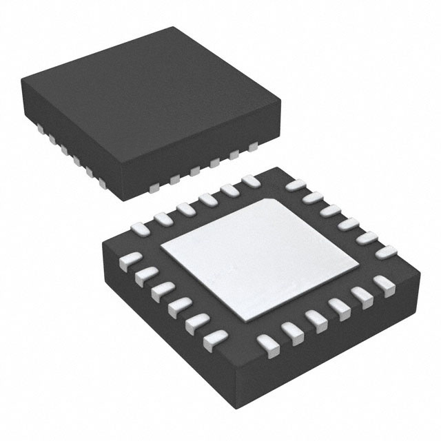


 工商网监
湘ICP备2023018690号
工商网监
湘ICP备2023018690号
