Product
Folder
Order
Now
Technical
Documents
Support &
Community
Tools &
Software
LP87521-Q1
LP87522-Q1, LP87523-Q1, LP87524-Q1, LP87525-Q1
SNVSB23 – MARCH 2018
LP8752x-Q1 10-A Buck Converter With Integrated Switches
1 Features
3 Description
•
•
The LP8752x-Q1 device is designed to meet the
power-management requirements of the latest
processors and platforms in various automotive
power applications. The device contains four stepdown DC/DC converter cores, which are configured
as a 4-phase output, 3-phase and 1-phase outputs,
2-phase and 2-phase outputs, one 2-phase and two
1-phase outputs, or four 1-phase outputs. The device
is controlled by an I2C-compatible serial interface and
by enable signals.
1
•
•
•
•
•
•
•
•
•
•
•
•
Qualified for Automotive Applications
AEC-Q100 Qualified With the Following Results:
– Device Temperature Grade 1: –40°C to
+125°C Ambient Operating Temperature
– Device HBM ESD Classification Level 2
– Device CDM ESD Classification Level C4B
Input Voltage: 2.8 V to 5.5 V
Output Voltage: 0.6 V to 3.36 V
Four High-Efficiency Step-Down DC/DC Converter
Cores:
– Maximum Output Current: 10 A
Switching Frequency: 2 MHz
Spread-Spectrum Mode and Phase Interleaving
Configurable General Purpose I/O (GPIOs)
I2C-Compatible Interface That Supports Standard
(100 kHz), Fast (400 kHz), Fast+ (1 MHz), and
High-Speed (3.4 MHz) Modes
Interrupt Function With Programmable Masking
Programmable Power-Good Signal (PGOOD)
Output Short-Circuit and Overload Protection
Overtemperature Warning and Protection
Overvoltage Protection (OVP) and Undervoltage
Lockout (UVLO)
2 Applications
Automotive Infotainment, Cluster, Radar, and
Camera Power Applications
space
VIN_B0
VIN_B1
SW_B0
VIN_B3
VANA
NRST
SDA
SCL
nINT
Configurable
multi-phase
SW_B2
SW_B3
FB_B0
Device Information(1)
PART NUMBER
LP87523-Q1
VQFN-HR (26)
4.50 mm × 4.00 mm
1-4
Outputs
LP87525-Q1
(1) For all available packages, see the orderable addendum at
the end of the data sheet.
FB_B1
FB_B2
Efficiency vs Output Current
FB_B3
100
PGOOD
GNDs
90
Efficiency (%)
EN2 (GPIO2)
EN3 (GPIO3)
BODY SIZE (NOM)
LP87522-Q1
CLKIN
EN1 (GPIO1)
PACKAGE
LP87524-Q1
SW_B1
VIN_B2
The LP8752x-Q1 device supports load-current
measurement without the addition of external currentsense resistors. The device also supports
programmable start-up and shutdown delays and
sequences synchronized to enable signals. The
sequences can include GPIO signals to control
external regulators, load switches, and processor
reset. During start-up and voltage change, the device
controls the output slew rate to minimize outputvoltage overshoot and in-rush current.
LP87521-Q1
Simplified Schematic
VIN
The automatic pulse-width-modulation (PWM) to
pulsed-frequency-modulation (PFM) operation (AUTO
mode), together with the automatic phase adding and
phase shedding, maximizes efficiency over a wide
output-current range. The LP8752x-Q1 supports
remote differential-voltage sensing for multiphase
outputs to compensate IR drop between the regulator
output and the point-of-load (POL) improving the
accuracy of the output voltage. The switching clock
can be forced to PWM mode and also synchronized
to an external clock to minimize the disturbances.
80
70
4PH, Vout=1.8V, Vin=3.7V
3PH, Vout=1.8V, Vin=3.7V
2PH, Vout=1.8V, Vin=3.7V
1PH, Vout=1.8V, Vin=3.7V
60
50
0.001
0.01
0.1
Output Current (A)
1
10
D531
1
An IMPORTANT NOTICE at the end of this data sheet addresses availability, warranty, changes, use in safety-critical applications,
intellectual property matters and other important disclaimers. PRODUCTION DATA.
�LP87521-Q1
LP87522-Q1, LP87523-Q1, LP87524-Q1, LP87525-Q1
SNVSB23 – MARCH 2018
www.ti.com
Table of Contents
1
2
3
4
5
6
7
Features ..................................................................
Applications ...........................................................
Description .............................................................
Revision History.....................................................
Device Comparison Table.....................................
Pin Configuration and Functions .........................
Specifications.........................................................
7.1
7.2
7.3
7.4
7.5
7.6
7.7
8
8.5 Programming........................................................... 36
8.6 Register Maps ......................................................... 39
1
1
1
2
3
3
5
9
9.1 Application Information............................................ 63
9.2 Typical Applications ................................................ 63
10 Power Supply Recommendations ..................... 82
11 Layout................................................................... 83
11.1 Layout Guidelines ................................................. 83
11.2 Layout Example .................................................... 84
Absolute Maximum Ratings ...................................... 5
ESD Ratings.............................................................. 5
Recommended Operating Conditions....................... 5
Thermal Information .................................................. 6
Electrical Characteristics........................................... 6
I2C Serial Bus Timing Requirements ...................... 12
Typical Characteristics ............................................ 14
12 Device and Documentation Support ................. 85
12.1
12.2
12.3
12.4
12.5
12.6
12.7
12.8
Detailed Description ............................................ 16
8.1
8.2
8.3
8.4
Overview .................................................................
Functional Block Diagram .......................................
Feature Descriptions ...............................................
Device Functional Modes........................................
Application and Implementation ........................ 63
16
17
17
34
Device Support......................................................
Documentation Support ........................................
Related Links ........................................................
Receiving Notification of Documentation Updates
Community Resources..........................................
Trademarks ...........................................................
Electrostatic Discharge Caution ............................
Glossary ................................................................
85
85
85
85
85
85
85
86
13 Mechanical, Packaging, and Orderable
Information ........................................................... 86
4 Revision History
2
DATE
REVISION
NOTES
March 2018
*
Initial Release
Submit Documentation Feedback
Copyright © 2018, Texas Instruments Incorporated
Product Folder Links: LP87521-Q1 LP87522-Q1 LP87523-Q1 LP87524-Q1 LP87525-Q1
�LP87521-Q1
LP87522-Q1, LP87523-Q1, LP87524-Q1, LP87525-Q1
www.ti.com
SNVSB23 – MARCH 2018
5 Device Comparison Table
PART NUMBER
DC/DC CONFIGURATIONS
LP87521-Q1
One 4-phase output
LP87522-Q1
One 3-phase and one 1-phase outputs
LP87523-Q1
One 2-phase and two 1-phase outputs
LP87524-Q1
Four 1-phase outputs
LP87525-Q1
Two 2-phase outputs
6 Pin Configuration and Functions
RNF Package
26-Pin VQFN-HR With Thermal Pad
Top View
VIN_B3
3
22
SW_B3
EN3
23
PGND_B23
2
24
SW_B2
FB_B2
25
VIN_B2
1
26
FB_B3
21
NRST
20
CLKIN
nINT
19
4
AGND
VANA
18
5
SCL
AGND
17
6
SDA
PGOOD
16
7
EN1
EN2
15
8
FB_B0
FB_B1
14
AGND
VIN_B0
SW_B0
PGND_B01
SW_B1
VIN_B1
Copyright © 2018, Texas Instruments Incorporated
9
10
11
12
13
Submit Documentation Feedback
Product Folder Links: LP87521-Q1 LP87522-Q1 LP87523-Q1 LP87524-Q1 LP87525-Q1
3
�LP87521-Q1
LP87522-Q1, LP87523-Q1, LP87524-Q1, LP87525-Q1
SNVSB23 – MARCH 2018
www.ti.com
Pin Functions
PIN
TYPE (1)
DESCRIPTION
NO.
NAME
1
FB_B2
A
2
EN3
D/I/O
3
CLKIN
D/I
External clock input. Connect this pin to ground if the external clock is not used.
4, 17,
Thermal
Pad
AGND
G
Ground
5
SCL
D/I
Serial interface clock input for I2C access. Connect this pin to a pullup resistor.
6
SDA
D/I/O
Serial interface data input and output for I2C access. Connect this pin to a pullup resistor.
7
EN1
D/I/O
Programmable enable signal for the buck regulators (can be also configured to select between
two buck output voltage levels). This pin functions alternatively as GPIO1.
8
FB_B0
A
Output voltage feedback (positive) for the BUCK0 converter.
9
VIN_B0
P
Input for the BUCK0 converter. The separate power pins, VIN_Bx, are not connected together
internally. The VIN_Bx pins must be connected together in the application and be locally
bypassed.
Output voltage feedback (positive) for the BUCK2 converter.
Programmable enable signal for the buck regulators (can be also configured to select between
two buck output-voltage levels). This pin functions alternatively as GPIO3.
10
SW_B0
A
BUCK0 switch node
11
PGND_B01
G
Power ground for the BUCK0 and BUCK1 converters
12
SW_B1
A
BUCK1 switch node
13
VIN_B1
P
Input for the BUCK1 converter. The separate power pins, VIN_Bx, are not connected together
internally. The VIN_Bx pins must be connected together in the application and be locally
bypassed.
14
FB_B1
A
Output voltage feedback (positive) for the BUCK1 converter. This pin functions alternatively as
the output ground feedback (negative) for the BUCK0 converter.
15
EN2
D/I/O
Programmable enable signal for the buck regulators (can be also configured to select between
two buck output voltage levels). This pin functions alternatively as GPIO2.
16
PGOOD
D/O
Power-good indication signal
18
VANA
P
19
nINT
D/O
Open-drain interrupt output. This pin is active low.
20
NRST
D/I
Reset signal for the device
21
FB_B3
A
Output voltage feedback (positive) for the BUCK3 converter. This pin functions alternatively as
the output ground feedback (negative) for the BUCK2 converter.
22
VIN_B3
P
Input for the BUCK3 converter. The separate power pins, VIN_Bx, are not connected together
internally. The VIN_Bx pins must be connected together in the application and be locally
bypassed.
Supply voltage for the analog and digital blocks. This pin must be connected to the same node
as VIN_Bx.
23
SW_B3
A
BUCK3 switch node
24
PGND_B23
G
Power ground for the BUCK2 and BUCK3 converters
25
SW_B2
A
BUCK2 switch node
26
VIN_B2
P
Input for the BUCK2 converter. The separate power pins, VIN_Bx, are not connected together
internally. The VIN_Bx pins must be connected together in the application and be locally
bypassed.
(1)
4
A: Analog Pin, D: Digital Pin, G: Ground Pin, P: Power Pin, I: Input Pin, O: Output Pin
Submit Documentation Feedback
Copyright © 2018, Texas Instruments Incorporated
Product Folder Links: LP87521-Q1 LP87522-Q1 LP87523-Q1 LP87524-Q1 LP87525-Q1
�LP87521-Q1
LP87522-Q1, LP87523-Q1, LP87524-Q1, LP87525-Q1
www.ti.com
SNVSB23 – MARCH 2018
7 Specifications
7.1 Absolute Maximum Ratings
Over operating free-air temperature range (unless otherwise noted) (1) (2)
MIN
MAX
UNIT
Voltage on power connections
VIN_Bx, VANA
–0.3
6
V
Voltage on buck switch nodes
SW_Bx
–0.3
(VIN_Bx + 0.3
V)
with 6 V
maximum
V
Voltage on buck voltage sense nodes
FB_Bx
–0.3
(VANA + 0.3 V)
with 6 V
maximum
V
Voltage on NRST input
NRST
–0.3
6
V
SDA, SCL, nINT, CLKIN
–0.3
6
V
EN1 (GPIO1), EN2 (GPIO2), EN3
(GPIO3), PGOOD
–0.3
(VANA + 0.3 V)
with 6 V
maximum
V
Voltage on logic pins (input or output pins)
Maximum lead temperature (soldering, 10 sec.)
260
°C
Junction temperature, TJ-MAX
–40
150
°C
Storage temperature, Tstg
–65
150
°C
(1)
(2)
Stresses beyond those listed under Absolute Maximum Ratings may cause permanent damage to the device. These are stress ratings
only, which do not imply functional operation of the device at these or any other conditions beyond those indicated under Recommended
Operating Conditions. Exposure to absolute-maximum-rated conditions for extended periods may affect device reliability.
All voltage values are with respect to network ground.
7.2 ESD Ratings
VALUE
Human-body model (HBM), per AEC Q100-002
V(ESD)
(1)
Electrostatic discharge
(1)
Charged-device model (CDM), per AEC Q100-011
UNIT
±2000
All pins
±500
Corner pins (1, 8,
14, and 21)
±750
V
AEC Q100-002 indicates that HBM stressing shall be in accordance with the ANSI/ESDA/JEDEC JS-001 specification.
7.3 Recommended Operating Conditions
Over operating free-air temperature range (unless otherwise noted)
MIN
MAX
UNIT
INPUT VOLTAGE
Voltage on power connections
VIN_Bx, VANA
2.8
5.5
V
VANA with
5.5 V maximum
V
Voltage on NRST
NRST
1.65
Voltage on logic pins (input or output pins)
nINT, CLKIN
1.65
5.5
V
0
VANA with
5.5 V maximum
V
Voltage on I C interface, standard (100 kHz), fast (400
SCL, SDA
khz), fast+ (1 MHz), and high-speed (3.4 MHz) modes
1.65
1.95
V
Voltage on I2C interface, standard (100 kHz), fast (400
SCL, SDA
kHz), and fast+ (1 MHz) modes
3.1
VANA with
3.6 V maximum
V
Junction temperature, TJ
–40
140
°C
Ambient temperature, TA
–40
125
°C
Voltage on logic pins (input or output pins)
ENx, PGOOD
2
TEMPERATURE
Copyright © 2018, Texas Instruments Incorporated
Submit Documentation Feedback
Product Folder Links: LP87521-Q1 LP87522-Q1 LP87523-Q1 LP87524-Q1 LP87525-Q1
5
�LP87521-Q1
LP87522-Q1, LP87523-Q1, LP87524-Q1, LP87525-Q1
SNVSB23 – MARCH 2018
www.ti.com
7.4 Thermal Information
LP8752x-Q1
THERMAL METRIC (1)
RNF (VQFN-HR)
UNIT
26 PINS
RθJA
Junction-to-ambient thermal resistance
34.6
°C/W
RθJC(top)
Junction-to-case (top) thermal resistance
16.5
°C/W
RθJB
Junction-to-board thermal resistance
4.7
°C/W
ψJT
Junction-to-top characterization parameter
0.6
°C/W
ψJB
Junction-to-board characterization parameter
4.7
°C/W
RθJC(bot)
Junction-to-case (bottom) thermal resistance
1.4
°C/W
(1)
For more information about traditional and new thermal metrics, see the Semiconductor and IC Package Thermal Metrics application
report.
7.5 Electrical Characteristics
–40°C ≤ TJ ≤ +140°C, CPOL = 22 µF/phase, specified VVANA, VVIN_Bx , VNRST, VVOUT_Bx, and IOUT range, unless otherwise noted.
Typical values are at TJ = 25°C, VVANA = VVIN_Bx = 3.7 V, and VOUT = 1 V, unless otherwise noted (1) (2).
PARAMETER
TEST CONDITIONS
MIN
TYP
MAX
UNIT
1.9
10
µF
10
22
µF
22
µF
EXTERNAL COMPONENTS
Connected from VIN_Bx to
PGND_Bx
CIN
Input filtering capacitance
COUT
Output filtering capacitance per phase, local
CPOL
Optional point-of-load (POL) capacitance per phase
COUT-TOTAL
ESRC
Total output capacitance (local and POL)
ESR of the input and output capacitor
L
Inductance of the inductor
DCRL
Inductor DCR
4-phase Output voltage slew-rate ≤ 3.8
output
mV/µs
1000
3-phase Output voltage slew-rate ≤ 3.8
output
mV/µs
750
2-phase Output voltage slew-rate ≤ 3.8
output
mV/µs
500
1-phase Output voltage slew-rate ≤ 3.8
output
mV/µs
250
µF
1 MHz ≤ f ≤ 10 MHz
2
10
0.47
–30%
mΩ
µH
30%
25
mΩ
BUCK REGULATOR
VVIN_Bx
Input voltage range
VVOUT_Bx
Programmable output voltage range
2.8
0.6
0.6 V ≤ VVOUT < 0.73 V
Output voltage step size
(1)
(2)
6
3.7
5.5
V
3.36
V
10
0.73 V ≤ VVOUT < 1.4 V
5
1.4 V ≤ VVOUT ≤ 3.36 V
20
mV
All voltage values are with respect to network ground.
Minimum (Min) and Maximum (Max) limits are specified by design, test, or statistical analysis. Typical (Typ) numbers are not verified, but
do represent the most likely norm.
Submit Documentation Feedback
Copyright © 2018, Texas Instruments Incorporated
Product Folder Links: LP87521-Q1 LP87522-Q1 LP87523-Q1 LP87524-Q1 LP87525-Q1
�LP87521-Q1
LP87522-Q1, LP87523-Q1, LP87524-Q1, LP87525-Q1
www.ti.com
SNVSB23 – MARCH 2018
Electrical Characteristics (continued)
–40°C ≤ TJ ≤ +140°C, CPOL = 22 µF/phase, specified VVANA, VVIN_Bx , VNRST, VVOUT_Bx, and IOUT range, unless otherwise noted.
Typical values are at TJ = 25°C, VVANA = VVIN_Bx = 3.7 V, and VOUT = 1 V, unless otherwise noted(1) (2).
PARAMETER
TEST CONDITIONS
MIN
TYP
4-phase VIN ≥ 3 V
output
2.8 V ≤ VIN < 3 V
Output current (3) The maximum output
current from device is 10A regardless of
device phase configurations.
IOUT
7.2
3-phase VIN ≥ 3 V
output
2.8 V ≤ VIN < 3 V
9.0
2-phase VIN ≥ 3 V
output
2.8 V ≤ VIN < 3 V
8.0
1-phase VIN ≥ 3 V
output
2.8 V ≤ VIN < 3 V
4.0
DC output voltage accuracy, includes voltage
reference, DC load and line regulations, process, and
temperature
6.5
3.0
0.5
–20
20
VOUT ≥ 1 V, PWM mode
–2%
2%
VOUT < 1 V, PFM mode
–20
40
–2%
2% +
20 mV
PWM mode, ESRC < 2 mΩ, L
4-phase = 0.47 µH
output
PFM mode, L = 0.47 µH
PWM mode, ESRC < 2 mΩ, L
3-phase = 0.47 µH
output
PFM mode, L = 0.47 µH
PWM mode, ESRC < 2 mΩ, L
2-phase = 0.47 µH
output
PFM mode, L = 0.47 µH
PWM mode, ESRC < 2 mΩ, L
1-phase = 0.47 µH
output,
PFM mode, L = 0.47 µH
DC line regulation
IOUT = IOUT(max)
DCLDR
DC load regulation in PWM mode
VOUT = 1 V, 0 A ≤ IOUT ≤
IOUT(max)
(3)
V
VOUT < 1 V, PWM mode
DCLNR
A
6.0
VOUT ≥ 1 V, PFM mode
Ripple voltage
UNIT
10
Input and output voltage difference
Minimum voltage between VIN_x and VOUT to fulfill
the electrical characteristics
VVOUT_DC
MAX
mV
mV
3
4
4
5
mVp-p
6
7
8
14
0.1
%/V
0.8%
The maximum output current can be limited by the forward current limit ILIM FWD and by the junction temperature. The power dissipation
inside the die depends on the length of the current pulse and efficiency and the junction temperature may increase to thermal shutdown
level if the board and ambient temperatures are high.
Copyright © 2018, Texas Instruments Incorporated
Submit Documentation Feedback
Product Folder Links: LP87521-Q1 LP87522-Q1 LP87523-Q1 LP87524-Q1 LP87525-Q1
7
�LP87521-Q1
LP87522-Q1, LP87523-Q1, LP87524-Q1, LP87525-Q1
SNVSB23 – MARCH 2018
www.ti.com
Electrical Characteristics (continued)
–40°C ≤ TJ ≤ +140°C, CPOL = 22 µF/phase, specified VVANA, VVIN_Bx , VNRST, VVOUT_Bx, and IOUT range, unless otherwise noted.
Typical values are at TJ = 25°C, VVANA = VVIN_Bx = 3.7 V, and VOUT = 1 V, unless otherwise noted(1) (2).
PARAMETER
TEST CONDITIONS
0 A ≤ IOUT ≤ 8 A, tr = tf = 10
µs, PWM mode, COUT = 22
µF/phase, L = 0.47 µH,
4-phase CPOL = 22 µF/phase
output
0.1 A ≤ IOUT ≤ 8 A, tr = tf = 1
µs, PWM mode, COUT = 22
µF/phase, L = 0.47 µH,
CPOL = 22 µF/phase
TLDSR
Transient load step response
0 A ≤ IOUT ≤ 6 A, tr = tf = 10
µs, PWM mode, COUT = 22
µF/phase, L = 0.47 µH,
3-phase CPOL = 22 µF/phase
output
0.1 A ≤ IOUT ≤ 6 A, tr = tf = 1
µs, PWM mode, COUT = 22
µF/phase, L = 0.47 µH,
CPOL = 22 µF/phase
0 A ≤ IOUT ≤ 4 A, tr = tf = 10
µs, PWM mode, COUT = 22
µF/phase, L = 0.47 µH,
2-phase CPOL = 22 µF/phase
output
0.1 A ≤ IOUT ≤ 4 A, tr = tf = 1
µs, PWM mode, COUT = 22
µF/phase, L = 0.47 µH,
CPOL = 22 µF/phase
0 A ≤ IOUT ≤ 2 A, tr = tf = 10
µs, PWM mode, COUT = 22
µF, L = 0.47 µH, CPOL =
1-phase 22 µF
output
0.1 A ≤ IOUT ≤ 2 A, tr = tf = 1
µs, PWM mode, COUT = 22
µF, L = 0.47 µH, CPOL =
22 µF
TLNSR
Transient line response
ILIM
ILIM
FWD
NEG
RDS(ON) HS
8
UNIT
±40
–3%
3%
±40
mV
–3%
3%
±40
–3%
3%
±40
±5
Step size
mV
5
0.5
A
Accuracy, VVIN_Bx ≥ 3 V, ILIM
≥3A
–5%
7.5%
20%
Accuracy, 2.8 V ≤ VVIN_Bx < 3
V, ILIM ≥ 3. A
–20%
7.5%
20%
1.6
2
2.4
A
On-resistance, high-side FET
Each phase, between VIN_Bx
and SW_Bx pins, I = 1 A
29
65
mΩ
On-resistance, low-side FET
Each phase, between SW_Bx
and PGND_Bx pins, I = 1 A
17
35
mΩ
2
2.2
MHz
FET
fSW
MAX
3%
1.5
Negative current limit per phase (peak for each
switching cycle)
FET
RDS(ON) LS
TYP
–3%
VVIN_Bx stepping 3 V ↔ 3.5 V,
tr = tf = 10 µs, IOUT = IOUT(max)
Programmable range
Forward current limit (peak for each switching cycle)
The max peak current limit of all combined phases
cannot exceed 14A.
MIN
Switching frequency, PWM mode
1.8
Current balancing for multiphase outputs
Current mismatch between
phases, IOUT > 1 A/phase
Start-up time (soft start)
From ENx to VOUT = 0.35 V
(slew-rate control begins),
COUT_TOTAL = 44 µF/phase
Submit Documentation Feedback
10%
200
µs
Copyright © 2018, Texas Instruments Incorporated
Product Folder Links: LP87521-Q1 LP87522-Q1 LP87523-Q1 LP87524-Q1 LP87525-Q1
�LP87521-Q1
LP87522-Q1, LP87523-Q1, LP87524-Q1, LP87525-Q1
www.ti.com
SNVSB23 – MARCH 2018
Electrical Characteristics (continued)
–40°C ≤ TJ ≤ +140°C, CPOL = 22 µF/phase, specified VVANA, VVIN_Bx , VNRST, VVOUT_Bx, and IOUT range, unless otherwise noted.
Typical values are at TJ = 25°C, VVANA = VVIN_Bx = 3.7 V, and VOUT = 1 V, unless otherwise noted(1) (2).
PARAMETER
Output voltage slew-rate (4)
MIN
TYP
MAX
COUT-TOTAL ≤ 80 µF/phase
TEST CONDITIONS
–15%
10
15%
COUT-TOTAL ≤ 130 µF/phase
–15%
7.5
15%
COUT-TOTAL ≤ 250 µF/phase
–15%
3.8
15%
COUT-TOTAL ≤ 500 µF/phase
–15%
1.9
15%
COUT-TOTAL ≤ 500 µF/phase
–15%
0.94
15%
COUT-TOTAL ≤ 500 µF/phase
–15%
0.47
15%
UNIT
mV/µs
IPFM-PWM
PFM-to-PWM current threshold (5)
600
mA
IPWM-PFM
PWM-to-PFM current threshold (5)
200
mA
IADD
Phase adding level (multiphase rails)
ISHED
Phase shedding level (multiphase rails)
Output pulldown resistance
Output voltage monitoring for PGOOD pin
From 1-phase to 2-phase
1
From 2-phase to 3-phase
2
From 3-phase to 4-phase
3
From 2-phase to 1-phase
0.7
From 3-phase to 2-phase
1.5
From 4-phase to 3-phase
2.4
Regulator disabled
Power-good threshold for status bit
BUCKx_PG_STAT
(4)
(5)
A
160
230
300
Overvoltage monitoring
(compared to DC outputvoltage level, VVOUT_DC)
39
50
64
Undervoltage monitoring
(compared to DC outputvoltage level, VVOUT_DC)
–53
Ω
mV
Debounce time during
regulator enable
PGOOD_SET_DELAY = 0h
4
Debounce time during
regulator enable
PGOOD_SET_DELAY = 1h
10
Deglitch time during operation
and after voltage change
Power-good threshold for interrupt BUCKx_PG_INT,
difference from final voltage
A
Rising ramp voltage, enable
or voltage change
Falling ramp voltage, voltage
change
During operation, status signal
is forced to 0h during voltage
change
–40
11
4
–29
10
µs
13
ms
10
µs
–20
–14
–8
8
14
20
–20
–14
–8
mV
mV
Output capacitance, forward and negative current limits and load current may limit the maximum and minimum slew rates. The actual
set fixed slew rate value for specific part number is listed in corresponding TRM document.
The final PFM-to-PWM and PWM-to-PFM switchover current varies slightly and is dependent on the output voltage, input voltage, and
the inductor current level.
Copyright © 2018, Texas Instruments Incorporated
Submit Documentation Feedback
Product Folder Links: LP87521-Q1 LP87522-Q1 LP87523-Q1 LP87524-Q1 LP87525-Q1
9
�LP87521-Q1
LP87522-Q1, LP87523-Q1, LP87524-Q1, LP87525-Q1
SNVSB23 – MARCH 2018
www.ti.com
Electrical Characteristics (continued)
–40°C ≤ TJ ≤ +140°C, CPOL = 22 µF/phase, specified VVANA, VVIN_Bx , VNRST, VVOUT_Bx, and IOUT range, unless otherwise noted.
Typical values are at TJ = 25°C, VVANA = VVIN_Bx = 3.7 V, and VOUT = 1 V, unless otherwise noted(1) (2).
PARAMETER
TEST CONDITIONS
MIN
TYP
MAX
UNIT
24
MHz
EXTERNAL CLOCK AND PLL
Nominal frequency of the external input clock
1
Nominal frequency step size of the external input
clock
1
Required accuracy from nominal frequency of the
external input clock
–30%
MHz
10%
Delay time for missing external clock detection
1.8
µs
Delay and debounce time for external clock detection
20
µs
Clock change delay (internal to external)
delay from valid clock detection to use of external
clock
600
µs
Cycle-to-cycle PLL output clock jitter
300
ps, pp
PROTECTION FUNCTIONS
Thermal warning
Temperature rising,
TDIE_WARN_LEVEL = 0h
115
125
135
Temperature rising,
TDIE_WARN_LEVEL = 1h
127
137
147
Temperature rising
140
150
°C
Thermal warning hysteresis
Thermal shutdown
20
Thermal shutdown hysteresis
VANAOVP
VANA overvoltage
20
VANA undervoltage lockout
°C
°C
Voltage rising
5.6
5.8
6.1
Voltage falling
5.45
5.73
5.96
Voltage rising
2.51
2.63
2.75
Voltage falling
2.5
2.6
2.7
VANA overvoltage hysteresis
VANAUVLO
°C
160
40
V
mV
V
LOAD CURRENT MEASUREMENT
Current measurement range
Output current for maximum
code
Resolution
LSB
Measurement accuracy
IOUT > 1 A
Measurement time
PFM mode (automatically
changing to PWM mode for
the measurement)
20.47
20
A
mA
< 10%
PWM mode
45
µs
4
CURRENT CONSUMPTION
10
Shutdown current consumption
From VANA and VIN_Bx pins,
NRST = 0 V, VANA = VIN_Bx
= 3.7 V
1.4
µA
Standby current consumption
From VANA and VIN_Bx pins,
NRST = 1.8 V, VANA =
VIN_Bx = 3.7 V, regulators
disabled
6.7
µA
Submit Documentation Feedback
Copyright © 2018, Texas Instruments Incorporated
Product Folder Links: LP87521-Q1 LP87522-Q1 LP87523-Q1 LP87524-Q1 LP87525-Q1
�LP87521-Q1
LP87522-Q1, LP87523-Q1, LP87524-Q1, LP87525-Q1
www.ti.com
SNVSB23 – MARCH 2018
Electrical Characteristics (continued)
–40°C ≤ TJ ≤ +140°C, CPOL = 22 µF/phase, specified VVANA, VVIN_Bx , VNRST, VVOUT_Bx, and IOUT range, unless otherwise noted.
Typical values are at TJ = 25°C, VVANA = VVIN_Bx = 3.7 V, and VOUT = 1 V, unless otherwise noted(1) (2).
PARAMETER
TEST CONDITIONS
MIN
TYP
MAX
UNIT
4-phase enabled: From VANA
and VIN_Bx pins, NRST = 1.8
V, VANA = VIN_Bx = 3.7 V,
IOUT = 0 mA, not switching,
one regulator enabled,
internal RC oscillator, PGOOD
monitoring enabled
77
3-phase enabled: From VANA
and VIN_Bx pins, NRST = 1.8
V, VANA = VIN_Bx = 3.7 V,
IOUT = 0 mA, not switching,
one regulator enabled,
internal RC oscillator, PGOOD
monitoring enabled
71
2-phase enabled: From VANA
and VIN_Bx pins, NRST = 1.8
V, VANA = VIN_Bx = 3.7 V,
IOUT = 0 mA, not switching,
one regulator enabled,
internal RC oscillator, PGOOD
monitoring enabled
65
1-phase enabled: From VANA
and VIN_Bx pins, NRST = 1.8
V, VANA = VIN_Bx = 3.7 V,
IOUT = 0 mA, not switching,
one regulator enabled,
internal RC oscillator, PGOOD
monitoring enabled
57
Active current consumption during PWM operation
Each phase
17
mA
PLL and clock detector current consumption
Additional current
consumption when internal
RC oscillator, clock detector
and PLL are enabled
2
mA
Active current consumption in PFM mode
µA
DIGITAL INPUT SIGNALS: NRST, EN1, EN2, EN3, EN4, SCL, SDA, GPIO1, GPIO2, GPIO3, CLKIN
VIL
Input low level
VIH
Input high level
1.2
VHYS
Hysteresis of Schmitt trigger inputs
10
77
650
1150
ENx pulldown resistance
ENx_PD = 1h
NRST pulldown resistance
Always present
0.4
V
200
mV
V
500
kΩ
1700
kΩ
DIGITAL OUTPUT SIGNALS: nINT
VOL
Output low level
ISOURCE = 2 mA
RP
External pullup resistor
To VIO supply
0.4
10
V
kΩ
DIGITAL OUTPUT SIGNALS: SDA
VOL
Output low level
ISOURCE = 10 mA
0.4
V
0.4
V
VVANA
V
VVANA
V
DIGITAL OUTPUT SIGNALS: PGOOD, GPIO1, GPIO2, GPIO3
VOL
Output low level
VOH
Output high level, configured to push-pull
VPU
Supply voltage for external pull-up resistor, configured
to open-drain
RPU
External pullup resistor, configured to open-drain
ISOURCE = 2 mA
VVANA –
0.4
ISINK = 2 mA
10
kΩ
ALL DIGITAL INPUTS
ILEAK
Input current
Copyright © 2018, Texas Instruments Incorporated
All logic inputs over pin
voltage range (except NRST)
−1
1
Submit Documentation Feedback
Product Folder Links: LP87521-Q1 LP87522-Q1 LP87523-Q1 LP87524-Q1 LP87525-Q1
µA
11
�LP87521-Q1
LP87522-Q1, LP87523-Q1, LP87524-Q1, LP87525-Q1
SNVSB23 – MARCH 2018
www.ti.com
7.6 I2C Serial Bus Timing Requirements
These specifications are ensured by design. VIN_Bx = 3.7 V, unless otherwise noted.
MIN
ƒSCL
Serial clock frequency
Standard mode
100
Fast mode
400
Fast mode+
3.4
High-speed mode, Cb = 400 pF
SCL low time
tSU;DAT
tHD;DAT
tSU;STA
SCL high time
Data setup time
Data hold time
Setup time for a start or a
repeated start condition
4.7
Fast mode
1.3
Fast mode+
0.5
High-speed mode, Cb = 100 pF
160
High-speed mode, Cb = 400 pF
320
tBUF
Hold time for a start or a repeated
start condition
Bus free time between a stop and
start condition
0.6
Fast mode+
0.26
Setup time for a stop condition
12
Submit Documentation Feedback
µs
High-speed mode, Cb = 400 pF
120
Standard mode
250
Fast mode
100
Fast mode+
50
High-speed mode
10
Standard mode
10
3450
Fast mode
10
900
Fast mode+
10
High-speed mode, Cb = 100 pF
10
70
High-speed mode, Cb = 400 pF
10
150
Standard mode
4.7
Fast mode
0.6
Fast mode+
0.26
High-speed mode
160
ns
ns
ns
ns
µs
ns
4
Fast mode
0.6
Fast mode+
0.26
High-speed mode
160
Standard mode
4.7
Fast mode
1.3
Fast mode+
0.5
µs
ns
µs
4
Fast mode
0.6
Fast mode+
0.26
High-speed mode
160
Fast mode
Rise time of SDA signal
ns
60
Standard mode
trDA
µs
High-speed mode, Cb = 100 pF
Standard mode
tSU;STO
MHz
4
Fast mode
Standard mode
tHD;STA
kHz
1.7
Standard mode
Standard mode
tHIGH
UNIT
1
High-speed mode, Cb = 100 pF
tLOW
MAX
µs
ns
1000
20
Fast mode+
300
120
High-speed mode, Cb = 100 pF
10
80
High-speed mode, Cb = 400 pF
20
160
ns
Copyright © 2018, Texas Instruments Incorporated
Product Folder Links: LP87521-Q1 LP87522-Q1 LP87523-Q1 LP87524-Q1 LP87525-Q1
�LP87521-Q1
LP87522-Q1, LP87523-Q1, LP87524-Q1, LP87525-Q1
www.ti.com
SNVSB23 – MARCH 2018
I2C Serial Bus Timing Requirements (continued)
These specifications are ensured by design. VIN_Bx = 3.7 V, unless otherwise noted.
MIN
MAX
Standard mode
tfDA
Fall time of SDA signal
300
Fast mode
20 × (VDD /
5.5 V)
300
Fast mode+
20 × (VDD /
5.5 V)
120
High-speed mode, Cb = 100 pF
10
80
High-speed mode, Cb = 400 pF
30
160
Standard mode
Rise time of SCL signal
trCL1
20
300
Fast mode+
Rise time of SCL signal after a
repeated start condition and after
an acknowledge bit
120
High-speed mode, Cb = 100 pF
10
40
High-speed mode, Cb = 400 pF
20
80
High-speed mode, Cb = 100 pF
10
80
High-speed mode, Cb = 400 pF
20
160
Standard mode
tfCL
Fall time of a SCL signal
Cb
Capacitive load for each bus line
(SCL and SDA)
tSP
Pulse width of spike suppressed
(SCL and SDA spikes that are
less than the indicated width are
suppressed)
ns
1000
Fast mode
trCL
UNIT
ns
ns
300
Fast mode
20 × (VDD /
5.5 V)
300
Fast mode+
20 × (VDD /
5.5 V)
120
High-speed mode, Cb = 100 pF
10
40
High-speed mode, Cb = 400 pF
20
80
400
Standard mode, fast mode and fast mode+
50
High-speed mode
10
ns
pF
ns
tBUF
SDA
tHD;STA
trCL
tfDA
tLOW
tfCL
trDA
tSP
SCL
tHD;STA
tSU;STA
tSU;STO
tHIGH
tHD;DAT
S
tSU;DAT
START
RS
P
S
REPEATED
START
STOP
START
Figure 1. I2C Timing
Copyright © 2018, Texas Instruments Incorporated
Submit Documentation Feedback
Product Folder Links: LP87521-Q1 LP87522-Q1 LP87523-Q1 LP87524-Q1 LP87525-Q1
13
�LP87521-Q1
LP87522-Q1, LP87523-Q1, LP87524-Q1, LP87525-Q1
SNVSB23 – MARCH 2018
www.ti.com
7.7 Typical Characteristics
Unless otherwise specified: TA = 25°C, VIN = 3.7 V, VOUT = 1 V, V(NRST) = 1.8 V, ƒSW = 2 MHz, L = 0.47 µH (TOKO
DFE252012PD-R47M), COUT = 22 µF / phase, CPOL = 22 µF / phase.
4
10
3.5
9
8
Input Current (PA)
Input Current (PA)
3
2.5
2
1.5
7
6
5
4
3
1
2
0.5
0
2.5
1
3
3.5
4
4.5
Input Voltage (V)
5
0
2.5
5.5
V(NRST) = 0 V
V(NRST) = 1.8 V
90
90
85
85
80
80
75
75
70
65
60
55
V(NRST) = 1.8 V
Load = 0 mA
3.5
90
85
85
80
80
75
75
70
65
60
55
4
4.5
Input Voltage (V)
5
5.5
D048
Load = 0 mA
Figure 5. PFM Mode Current Consumption vs Input Voltage,
One Regulator Enabled (3+1-Phase Output)
Input Current (PA)
Input Current (PA)
3
V(NRST) = 1.8 V
90
70
65
60
55
50
2PH
1PH
45
40
2.5
3PH
1PH
D047
50
3
V(NRST) = 1.8 V
3.5
4
4.5
Input Voltage (V)
5
45
5.5
Load = 0 mA
Submit Documentation Feedback
40
2.5
3
D049
Figure 6. PFM Mode Current Consumption vs Input Voltage,
One Regulator Enabled (2+1+1-Phase Output)
14
40
2.5
5.5
Figure 4. PFM Mode Current Consumption vs Input Voltage
(4-Phase Output)
D046
Regulators disabled
55
45
5
5.5
60
50
4
4.5
Input Voltage (V)
5
65
45
3.5
4
4.5
Input Voltage (V)
70
50
3
3.5
Figure 3. Standby Current Consumption vs Input Voltage
Input Current (PA)
Input Current (PA)
Figure 2. Shutdown Current Consumption vs Input Voltage
40
2.5
3
D045
V(NRST) = 1.8 V
3.5
4
4.5
Input Voltage (V)
5
5.5
D051
Load = 0 mA
Figure 7. PFM Mode Current Consumption vs Input Voltage,
One Regulator Enabled (1+1+1+1-Phase Output)
Copyright © 2018, Texas Instruments Incorporated
Product Folder Links: LP87521-Q1 LP87522-Q1 LP87523-Q1 LP87524-Q1 LP87525-Q1
�LP87521-Q1
LP87522-Q1, LP87523-Q1, LP87524-Q1, LP87525-Q1
www.ti.com
SNVSB23 – MARCH 2018
Typical Characteristics (continued)
Unless otherwise specified: TA = 25°C, VIN = 3.7 V, VOUT = 1 V, V(NRST) = 1.8 V, ƒSW = 2 MHz, L = 0.47 µH (TOKO
DFE252012PD-R47M), COUT = 22 µF / phase, CPOL = 22 µF / phase.
90
85
Input Current (PA)
80
75
70
65
60
55
50
45
40
2.5
3
V(NRST) = 1.8 V
3.5
4
4.5
Input Voltage (V)
5
5.5
D050
Load = 0 mA
Figure 8. PFM Mode Current Consumption vs Input Voltage, One Regulator Enabled (2+2-Phase Output)
Copyright © 2018, Texas Instruments Incorporated
Submit Documentation Feedback
Product Folder Links: LP87521-Q1 LP87522-Q1 LP87523-Q1 LP87524-Q1 LP87525-Q1
15
�LP87521-Q1
LP87522-Q1, LP87523-Q1, LP87524-Q1, LP87525-Q1
SNVSB23 – MARCH 2018
www.ti.com
8 Detailed Description
8.1 Overview
The LP8752x-Q1 is a high-efficiency, high-performance power supply device with four step-down DC/DC
converter cores for automotive applications. Table 1 lists the output characteristics of the regulators.
NOTE
Maximum output current is given as the maximum capability per rail. For each device the
total combined output current must not exceed 10 A.
Table 1. Supply Specification
OUTPUT
DEVICE
LP87521-Q1
SUPPLY
VOUT RANGE
RESOLUTION
IMAX MAXIMUM OUTPUT
CURRENT
BUCK0, BUCK1, BUCK2, BUCK3
in one 4-phase output
0.6 to 3.36 V
10 mV (0.6 V to 0.73 V)
5 mV (0.73 V to 1.4 V)
20 mV (1.4 V to 3.36 V)
10 A
BUCK0, BUCK1, BUCK2
in one 3-phase output
0.6 to 3.36 V
10 mV (0.6 V to 0.73 V)
5 mV (0.73 V to 1.4 V)
20 mV (1.4 V to 3.36 V)
9A
BUCK3 in 1-phase output
0.6 to 3.36 V
10 mV (0.6 V to 0.73 V)
5 mV (0.73 V to 1.4 V)
20 mV (1.4 V to 3.36 V)
4A
BUCK0, BUCK1
in one 2-phase output
0.6 to 3.36 V
10 mV (0.6 V to 0.73 V)
5 mV (0.73 V to 1.4 V)
20 mV (1.4 V to 3.36 V)
8A
BUCK2 in 1-phase output
0.6 to 3.36 V
10 mV (0.6 V to 0.73 V)
5 mV (0.73 V to 1.4 V)
20 mV (1.4 V to 3.36 V)
4A
BUCK3 in 1-phase output
0.6 to 3.36 V
10 mV (0.6 V to 0.73 V)
5 mV (0.73 V to 1.4 V)
20 mV (1.4 V to 3.36 V)
4A
BUCK0 in 1-phase output
0.6 to 3.36 V
10 mV (0.6 V to 0.73 V)
5 mV (0.73 V to 1.4 V)
20 mV (1.4 V to 3.36 V)
4A
BUCK1 in 1-phase output
0.6 to 3.36 V
10 mV (0.6 V to 0.73 V)
5 mV (0.73 V to 1.4 V)
20 mV (1.4 V to 3.36 V)
4A
BUCK2 in 1-phase output
0.6 to 3.36 V
10 mV (0.6 V to 0.73 V)
5 mV (0.73 V to 1.4 V)
20 mV (1.4 V to 3.36 V)
4A
BUCK3 in 1-phase output
0.6 to 3.36 V
10 mV (0.6 V to 0.73 V)
5 mV (0.73 V to 1.4 V)
20 mV (1.4 V to 3.36 V)
4A
BUCK0, BUCK1
in 2-phase output
0.6 to 3.36 V
10 mV (0.6 V to 0.73 V)
5 mV (0.73 V to 1.4 V)
20 mV (1.4 V to 3.36 V)
8A
BUCK2, BUCK3
in 2-phase output
0.6 to 3.36 V
10 mV (0.6 V to 0.73 V)
5 mV (0.73 V to 1.4 V)
20 mV (1.4 V to 3.36 V)
8A
LP87522-Q1
LP87523-Q1
LP87524-Q1
LP87525-Q1
The LP8752x-Q1 also supports switching clock synchronization to an external clock. The nominal frequency of
the external clock can be from 1 MHz to 24 MHz with 1-MHz steps.
Additional features include:
• Soft start
• Input voltage protection:
– Undervoltage lockout
– Overvoltage protection
• Output voltage monitoring and protection:
– Overvoltage monitoring
– Undervoltage monitoring
– Overload protection
• Thermal warning
16
Submit Documentation Feedback
Copyright © 2018, Texas Instruments Incorporated
Product Folder Links: LP87521-Q1 LP87522-Q1 LP87523-Q1 LP87524-Q1 LP87525-Q1
�LP87521-Q1
LP87522-Q1, LP87523-Q1, LP87524-Q1, LP87525-Q1
www.ti.com
•
SNVSB23 – MARCH 2018
Thermal shutdown
Three enable signals can be multiplexed to general purpose I/O (GPIO) signals. The direction and output type
(open-drain or push-pull) are programmable for the GPIOs.
8.2 Functional Block Diagram
VANA
Buck0
nINT
Interrupts
ILIM Det
Pwrgood Det
Overload
and SC Det
Iload ADC
Enable,
Roof/Floor,
Slew-Rate
Control
EN1 (GPIO1)
EN2 (GPIO2)
EN3 (GPIO3)
Buck1
ILIM Det
SDA
SCL
Pwrgood Det
Overload
and SC Det
Iload ADC
I2C
PGOOD
Registers
OTP
EPROM
Buck2
ILIM Det
UVLO
Pwrgood Det
Digital
Logic
Thermal
Monitor
NRST
Overload
and SC Det
Iload ADC
Buck3
ILIM Det
SW
Reset
Ref &
Bias
Oscillator
Pwrgood Det
Overload
and SC Det
Iload ADC
CLKIN
Copyright © 2017, Texas Instruments Incorporated
8.3 Feature Descriptions
8.3.1 Multi-Phase DC/DC Converters
8.3.1.1 Overview
The LP8752x-Q1 includes four step-down DC/DC converter cores which can be configured for:
• 4-phase single output
• 3-phase and single-phase outputs
• dual-phase and two single-phase outputs
• four single-phase outputs
• two dual-phase outputs
The cores are designed for flexibility; most of the functions are programmable, thus allowing optimization of the
regulator operation for each application.
The LP8752x-Q1 has the following features:
• DVS support
• Automatic mode control based on the loading (PFM or PWM mode)
• Forced-PWM mode operation
• Optional external clock input to minimize crosstalk
• Optional spread spectrum technique to decrease EMI
• Phase control for optimized EMI
Copyright © 2018, Texas Instruments Incorporated
Submit Documentation Feedback
Product Folder Links: LP87521-Q1 LP87522-Q1 LP87523-Q1 LP87524-Q1 LP87525-Q1
17
�LP87521-Q1
LP87522-Q1, LP87523-Q1, LP87524-Q1, LP87525-Q1
SNVSB23 – MARCH 2018
www.ti.com
Feature Descriptions (continued)
•
•
•
•
•
•
•
•
•
Synchronous rectification
Current mode loop with PI compensator
Soft start
Power-Good flag with maskable interrupt
Power-Good signal (PGOOD) with selectable sources
Average output current sensing (for PFM entry, phase shedding/adding, and load current measurement)
Current balancing between the phases of the converter
Differential voltage sensing from point of the load for multiphase output
Dynamic phase shedding/adding, each output being phase shifted
The following parameters can be programmed via registers:
• Output voltage
• Forced-PWM operation
• Forced multiphase operation for multiphase outputs (forces also the PWM operation)
• Enable and disable delays for regulators and GPIOs controlled by ENx pins
There are two modes of operation for the converter, depending on the output current required: pulse-width
modulation (PWM) and pulse-frequency modulation (PFM). The converter operates in PWM mode at high load
currents of approximately 600 mA or higher. When operating in PWM mode the phases of a multiphase regulator
are automatically added/shedded based on the load current level. Lighter output current loads cause the
converter to automatically switch into PFM mode for decreased current consumption when forced-PWM mode is
disabled. The forced multiphase mode can be enabled for highest transient performance.
A multiphase synchronous buck converter offers several advantages over one power stage converter. For
application processor power delivery, lower ripple on the input and output currents and faster transient response
to load steps are the most significant advantages. Also, because the load current is evenly shared among
multiple channels in multiphase output configuration, the heat generated is greatly decreased for each channel
due to the fact that power loss is proportional to square of current. The physical size of the output inductor
shrinks significantly due to this heat reduction. Figure 9 shows a block diagram of a single core.
Interleaving switching action of the multiphase converters is shown in Figure 10.
+
-
Slave
Phase
Control
±
+
Voltage
Setting
Slew Rate
Control
VDAC
Programmable
Parameters
Slave
Interface
+
-
VIN
POS
Current
Limit
Ramp
Generator
+
FBP
FBN
PMOS
Current
Sense
Differential to SingleEnded
±
VOUT
Gate
Control
Error
Amp
Power
Good
Control
Block
Loop
Comp
Master
Interface
SW
NEG
Current
Limit
NMOS
Current
Sense
Zero
Cross
Detect
IADC
GND
Copyright © 2017, Texas Instruments Incorporated
Figure 9. Detailed Block Diagram Showing One Core
18
Submit Documentation Feedback
Copyright © 2018, Texas Instruments Incorporated
Product Folder Links: LP87521-Q1 LP87522-Q1 LP87523-Q1 LP87524-Q1 LP87525-Q1
�LP87521-Q1
LP87522-Q1, LP87523-Q1, LP87524-Q1, LP87525-Q1
www.ti.com
SNVSB23 – MARCH 2018
Feature Descriptions (continued)
IL_TOT_4PH
IL0
IL1
IL2
IL3
0
90
180
270
360
450
540
630
720
360
450
540
630
720
PWM0
PWM1
PWM2
PWM3
Switching Cycle 360º
0
90
180
270
Phase (Degrees)
(1)
Graph is not in scale and is for illustrative purposes only.
Figure 10. Example of PWM Timings, Inductor Current Waveforms, and Total Output Current in 4-Phase
Configuration.
8.3.1.2 Multiphase Operation, Phase Adding, and Phase-Shedding
Under heavy load conditions, the 4-phase converter switches each channel 90° apart. As a result, the 4-phase
converter has an effective ripple frequency four times greater than the switching frequency of any one phase. In
the same way 3-phase converter has an effective ripple frequency three times greater and 2-phase converter has
an effective ripple frequency two times greater than the switching frequency of any one phase. However, the
parallel operation decreases the efficiency at light load conditions. In order to overcome this operational
inefficiency, the LP8752x-Q1 can change the number of active phases to optimize efficiency for the variations of
the load. This is called phase adding/shedding. The concept is shown in Figure 11.
The converter can be forced to multiphase operation by the BUCKx_FPWM_MP bit in BUCKx_CTRL1 register. If
the regulator operates in forced multiphase mode (two phases in the dual-phase configuration, three phases in
three-phase configuration and four phases in a four-phase configuration) the forced-PWM operation is
automatically used. If the multiphase operation is not forced, the number of phases are added and shedded
automatically to follow the required output current.
Copyright © 2018, Texas Instruments Incorporated
Submit Documentation Feedback
Product Folder Links: LP87521-Q1 LP87522-Q1 LP87523-Q1 LP87524-Q1 LP87525-Q1
19
�LP87521-Q1
LP87522-Q1, LP87523-Q1, LP87524-Q1, LP87525-Q1
SNVSB23 – MARCH 2018
www.ti.com
Feature Descriptions (continued)
4-Phase
Operation
3-Phase
Operation
2-Phase
Operation
1-Phase
Operation
Best efficiency obtained with
Efficiency
N=1
N=2
N=3
N=4
Load Current
(1)
Graph is not in scale and is for illustrative purposes only.
Figure 11. Multiphase Buck Converter Efficiency vs Number of Phases (Converters in PWM Mode)
8.3.1.3 Transition Between PWM and PFM Modes
Normal PWM mode operation with phase-adding/shedding optimizes efficiency at mid-to-full load at the expense
of light-load efficiency. The LP8752x-Q1 converter operates in PWM mode at load current of about 600 mA or
higher. At lighter load-current levels the device automatically switches into PFM mode for decreased current
consumption when forced-PWM mode is disabled (AUTO-mode operation). By combining the PFM and the PWM
modes a high efficiency is achieved over a wide output-load-current range.
8.3.1.4 Multiphase Switcher Configurations
In single 4-phase output configuration the BUCK0 is master for the BUCK0, BUCK1, BUCK2, BUCK3 output, in
3-phase and single-phase outputs configuration the BUCK0 is master for the multiphase output BUCK0, BUCK1,
BUCK2, in 2-phase and two single-phase outputs configuration the BUCK0 is master for the BUCK0, BUCK1
output and in two 2-phase outputs configuration the BUCK0 is master for BUCK0, BUCK1 output, and the
BUCK2 is master for BUCK2, BUCK3 output.
In the multiphase configuration the control of the multiphase regulator settings is done using the control registers
of the master buck. The following slave registers are ignored:
• BUCKx_CTRL1 register, except EN_RDISx bit
• BUCKx_VOUT register
• BUCKx_FLOOR_VOUT register
• BUCKx_DELAY register
• interrupt bits related to the slave buck, except BUCKx_ILIM_INT
8.3.1.5 Buck Converter Load-Current Measurement
Buck load current can be monitored via I2C registers. The monitored buck converter is selected with the
LOAD_CURRENT_BUCK_SELECT[1:0] bits in SEL_I_LOAD register. A write to this selection register starts a
current measurement sequence. The regulator is forced to PWM mode during the measurement. The
measurement sequence is 50 µs long, maximum. The LP8752x-Q1 device can be configured to give out an
interrupt (I_LOAD_READY bit in INT_TOP1 register) after the load current measurement sequence is finished.
20
Submit Documentation Feedback
Copyright © 2018, Texas Instruments Incorporated
Product Folder Links: LP87521-Q1 LP87522-Q1 LP87523-Q1 LP87524-Q1 LP87525-Q1
�LP87521-Q1
LP87522-Q1, LP87523-Q1, LP87524-Q1, LP87525-Q1
www.ti.com
SNVSB23 – MARCH 2018
Feature Descriptions (continued)
Load current measurement interrupt can be masked with I_LOAD_READY_MASK bit (TOP_MASK1 register).
The measurement result can be read from registers I_LOAD_1 and I_LOAD_2. Register I_LOAD_1 bits
BUCK_LOAD_CURRENT[7:0] give out the LSB bits and register I_LOAD_2 bits BUCK_LOAD_CURRENT[9:8]
the MSB bits. The measurement result BUCK_LOAD_CURRENT[9:0] LSB is 20 mA, and maximum value of the
measurement corresponds to 20.46 A. If the selected buck regulator is a master phase, the measured current is
the total value of the master and slave phases. If the selected buck regulator is single-phase or slave phase, the
measured current is the output current of the selected phase.
8.3.1.6 Spread-Spectrum Mode
Radiated Energy
Power Spectrum is
Spread and Lowered
Systems with periodic switching signals may generate a large amount of switching noise in a set of narrowband
frequencies (the switching frequency and its harmonics). The usual solution to decrease noise coupling is to add
EMI filters and shields to the boards. The LP8752x-Q1 device has register-selectable spread-spectrum mode
which minimizes the need for output filters, ferrite beads, or chokes. In spread-spectrum mode, the switching
frequency varies around the center frequency, reducing the EMI emissions radiated by the converter and
associated passive components and PCB traces (see Figure 12). This feature is available only when internal RC
oscillator is used (PLL_MODE[1:0] = 00 in PLL_CTRL register), and it is enabled with the EN_SPREAD_SPEC
bit (PIN_FUNCTION register), and it affects all the buck cores.
Frequency
Where a fixed-frequency converter exhibits large amounts of spectral energy at the switching frequency, the spreadspectrum architecture of the LP8752x-Q1 spreads that energy over a large bandwidth.
Figure 12. Spread-Spectrum Modulation
8.3.2 Sync Clock Functionality
The LP8752x-Q1 device contains a CLKIN input to synchronize the switching clock of the buck regulator with the
external clock. The block diagram of the clocking and PLL module is shown in Figure 13. Depending on the
PLL_MODE[1:0] bits (in PLL_CTRL register) and the external clock availability, the external clock is selected,
and interrupt is generated, as shown in Table 2. The interrupt can be masked with SYNC_CLK_MASK bit in
TOP_MASK1 register. The nominal frequency of the external input clock is set by EXT_CLK_FREQ[4:0] bits (in
PLL_CTRL register), and it can be from 1 MHz to 24 MHz with 1-MHz steps. The external clock must be inside
accuracy limits (–30%/+10%) for valid clock detection.
The NO_SYNC_CLK interrupt (in INT_TOP1 register) is also generated in cases when the external clock is
expected but it is not available. These cases are start-up (read OTP-to-STANDBY transition) when
PLL_MODE[1:0] = 01 and regulator enable (STANDBY-to-ACTIVE transition) when PLL_MODE[1:0] = 10.
Copyright © 2018, Texas Instruments Incorporated
Submit Documentation Feedback
Product Folder Links: LP87521-Q1 LP87522-Q1 LP87523-Q1 LP87524-Q1 LP87525-Q1
21
�LP87521-Q1
LP87522-Q1, LP87523-Q1, LP87524-Q1, LP87525-Q1
SNVSB23 – MARCH 2018
www.ti.com
Feature Descriptions (continued)
24-MHz
RC
Oscillator
Internal
24-MHz
clock
CLKIN
Detector
Divider
´(;7_CLK_
)5(4´
CLKIN
1MHz
24MHz
Clock Select
Logic
PLL
´3//_02'(´
1MHz
Divider
24
Copyright © 2017, Texas Instruments Incorporated
Figure 13. Clock and PLL Module
Table 2. PLL Operation
DEVICE
OPERATION MODE
PLL_MODE[1:0]
PLL AND CLOCK
DETECTOR STATE
INTERRUPT FOR
EXTERNAL CLOCK
CLOCK
STANDBY
0h
Disabled
No
Internal RC
ACTIVE
0h
Disabled
No
Internal RC
STANDBY
1h
Enabled
When external clock
appears or disappears
Automatic change to external
clock when available
ACTIVE
1h
Enabled
When external clock
appears or disappears
Automatic change to external
clock when available
STANDBY
2h
Disabled
No
Internal RC
Enabled
When external clock
appears or disappears
Automatic change to external
clock when available
ACTIVE
2h
STANDBY
3h
Reserved
ACTIVE
3h
Reserved
8.3.3 Power-Up
The power-up sequence for the LP8752x-Q1 is as follows:
• VANA (and VIN_Bx) reach minimum recommended level (VVANA > VANAUVLO).
• NRST is set to high level (or shorted to VANA). This initiates power-on-reset (POR), OTP reading and
enables the system I/O interface. The I2C host must wait at least 1.2 ms before writing or reading data to the
LP8752x-Q1.
• Device goes to the STANDBY mode.
• The host can change the default register setting by I2C if needed.
• The regulator(s) can be enabled/disabled by ENx pin(s) and by I2C interface.
22
Submit Documentation Feedback
Copyright © 2018, Texas Instruments Incorporated
Product Folder Links: LP87521-Q1 LP87522-Q1 LP87523-Q1 LP87524-Q1 LP87525-Q1
�LP87521-Q1
LP87522-Q1, LP87523-Q1, LP87524-Q1, LP87525-Q1
www.ti.com
SNVSB23 – MARCH 2018
8.3.4 Regulator Control
8.3.4.1 Enabling and Disabling Regulators
The regulator(s) can be enabled when the device is in STANDBY or ACTIVE state. There are two ways for
enable and disable the regulators:
• Using EN_BUCKx bit in BUCKx_CTRL1 register (EN_PIN_CTRLx register bit is 0h)
• Using EN1, EN2, EN3 control pins (EN_BUCKx bit is 1h AND EN_PIN_CTRLx register bit is 1 in
BUCKx_CTRL1 register)
If the EN1, EN2, EN3 control pins are used for enable and disable then the control pin is selected with
BUCKx_EN_PIN_SELECT[1:0] bits (in BUCKx_CTRL1 register). The delay from the control signal rising edge to
enabling of the regulator is set by BUCKx_STARTUP_DELAY[3:0] bits, and the delay from control signal falling
edge to disabling of the regulator is set by BUCKx_SHUTDOWN_DELAY[3:0] bits in BUCKx_DELAY register.
The delays are valid only for EN1, EN2, EN3 signal control. The control with EN_BUCKx bit is immediate without
the delays.
The control of the regulator (with 0-ms delays) is shown in Table 3.
NOTE
The control of the regulator cannot be changed from one ENx pin to a different ENx pin
because the control is ENx signal-edge sensitive. The control from ENx pin to register bit
and back to the original ENx pin can be done during operation.
Table 3. Regulator Control
CONTROL
METHOD
EN_BUCKx
EN_PIN_CTRLx
BUCKx_EN_PI
N_SELECT[1:0]
EN_ROOF_FLOOR
x
EN1 PIN
EN2 PIN
EN3 PIN
BUCKx
OUTPUT VOLTAGE
Enable and
disable control
with EN_BUCKx
bit
0h
Don't Care
Don't Care
Don't Care
Don't Care
Don't Care
Don't Care
Disabled
1h
0h
Don't Care
Don't Care
Don't Care
Don't Care
Don't Care
BUCKx_VSET[7:0]
Enable and
disable control
with EN1 pin
1h
1h
0h
0h
Low
Don't Care
Don't Care
Disabled
1h
1h
0h
0h
High
Don't Care
Don't Care
BUCKx_VSET[7:0]
Enable and
disable control
with EN2 pin
1h
1h
1h
0h
Don't Care
Low
Don't Care
Disabled
1h
1h
1h
0h
Don't Care
High
Don't Care
BUCKx_VSET[7:0]
Enable and
disable control
with EN3 pin
1h
1h
2h
0h
Don't Care
Don't Care
Low
Disabled
1h
1h
2h
0h
Don't Care
Don't Care
High
BUCKx_VSET[7:0]
Roof and floor
control with EN1
pin
1h
1h
0h
1h
Low
Don't Care
Don't Care
BUCKx_FLOOR_VSET[7:0]
1h
1h
0h
1h
High
Don't Care
Don't Care
BUCKx_VSET[7:0]
Roof and floor
control with EN2
pin
1h
1h
1h
1h
Don't Care
Low
Don't Care
BUCKx_FLOOR_VSET[7:0]
1h
1h
1h
1h
Don't Care
High
Don't Care
BUCKx_VSET[7:0]
Roof and floor
control with EN3
pin
1h
1h
2h
1h
Don't Care
Don't Care
Low
BUCKx_FLOOR_VSET[7:0]
1h
1h
2h
1h
Don't Care
Don't Care
High
BUCKx_VSET[7:0]
The regulator is enabled by the ENx pin or by I2C writing as shown in Figure 14. The soft-start circuit limits the inrush current during start-up. When the output voltage rises to 0.35-V level, the output voltage becomes slew-rate
controlled. If there is a short circuit at the output and the output voltage does not increase above 0.35-V level in 1
ms, the regulator is disabled, and interrupt is set. When the output voltage reaches the Power-Good threshold
level the BUCKx_PG_INT interrupt flag (in INT_BUCK_x register) is set. The Power-Good interrupt flag can be
masked using BUCKx_PG_MASK bit (in BUCKx_MASK register).
The ENx input pins have integrated pulldown resistors. The pulldown resistors are enabled by default, and the
host can disable those with ENx_PD bits (in CONFIG register).
Copyright © 2018, Texas Instruments Incorporated
Submit Documentation Feedback
Product Folder Links: LP87521-Q1 LP87522-Q1 LP87523-Q1 LP87524-Q1 LP87525-Q1
23
�LP87521-Q1
LP87522-Q1, LP87523-Q1, LP87524-Q1, LP87525-Q1
SNVSB23 – MARCH 2018
www.ti.com
Voltage decrease because of load
No new Powergood interrupt
Voltage
BUCKx_VSET[7:0]
Powergood
Ramp 3.8 mV/Ps
0.6V
0.35V
Resistive pull-down
(if enabled)
Soft start
Time
Enable
BUCK_x_STAT(BUCKx_STAT)
0
BUCK_x_STAT(BUCKx_PG_STAT)
0
1
INT_BUCK_x(BUCKx_PG_INT)
0
1
1
0
0
1
0
0
nINT
Powergood
interrupt
Host clears
interrupt
Figure 14. Regulator Enable and Disable
8.3.4.2 Changing Output Voltage
The output voltage of the regulator can be changed by the ENx pin (voltage levels defined by the BUCKx_VOUT
and BUCKx_FLOOR_VOUT registers) or by writing to the BUCKx_VOUT and BUCKx_FLOOR_VOUT registers.
The voltage change is always slew-rate controlled. During voltage change the forced-PWM mode is used
automatically. If the multiphase operation is forced by the BUCKx_FPWM_MP bit (in BUCKx_CTRL1 register),
the regulator operates in multiphase mode (two phases in dual-phase configuration, 3 phases in 3-phase
configuration, and 4 phases in 4-phase configuration). If the multiphase operation is not forced, the number of
phases are added and shedded automatically to follow the required slew rate. When the programmed output
voltage is achieved, the mode becomes the one defined by the load current and the BUCKx_FPWM and
BUCKx_FPWM_MP bits in BUCKx_CTRL1 register.
The Power-Good interrupt is generated when the output voltage reaches the programmed voltage level, as
shown in Figure 15.
24
Submit Documentation Feedback
Copyright © 2018, Texas Instruments Incorporated
Product Folder Links: LP87521-Q1 LP87522-Q1 LP87523-Q1 LP87524-Q1 LP87525-Q1
�LP87521-Q1
LP87522-Q1, LP87523-Q1, LP87524-Q1, LP87525-Q1
www.ti.com
SNVSB23 – MARCH 2018
Voltage
BUCKx_VSET
Powergood
Ramp 3.8 mV/Ps
Powergood
BUCKx_FLOOR_VSET
Time
ENx
BUCKx_STAT(BUCKx_STAT)
1
BUCKx_STAT(BUCKx_PG_STAT)
1
INT_BUCKx(BUCKx_PG_INT)
0
0
1
1
0
0
1
1
nINT
Powergood
interrupt
Host clears
interrupt
Powergood
interrupt
Host clears
interrupt
Figure 15. Regulator Output Voltage Change With ENx pin
8.3.5 Enable and Disable Sequences
The LP8752x-Q1 device supports start-up and shutdown sequencing with programmable delays for different
regulator outputs using one EN1, EN2, EN3 control signal. The regulator is selected for delayed control with:
• EN_BUCKx = 1 (in BUCKx_CTRL1 register)
• EN_PIN_CTRLx = 1 (in BUCKx_CTRL1 register)
• EN_ROOF_FLOORx = 0 (in BUCKx_CTRL1 register)
• BUCKx_VSET[7:0] = Required voltage when ENx is high (in BUCKx_VOUT register)
• The ENABLE pin for control is selected with BUCKx_EN_PIN_SELECT[1:0] (in BUCKx_CTRL1 register)
• The delay from rising edge of ENx signal to the regulator enable is set by BUCKx_STARTUP_DELAY[3:0]
bits (in BUCKx_DELAY register) and
• The delay from falling edge of ENx signal to the regulator disable is set by BUCKx_SHUTDOWN_DELAY[3:0]
bits (in BUCKx_DELAY register)
There are four time steps available for start-up and shutdown sequences. The delay times are selected with
DOUBLE_DELAY bit in CONFIG register and HALF_DELAY bit in PGOOD_CTRL2 register as shown in Table 4.
Copyright © 2018, Texas Instruments Incorporated
Submit Documentation Feedback
Product Folder Links: LP87521-Q1 LP87522-Q1 LP87523-Q1 LP87524-Q1 LP87525-Q1
25
�LP87521-Q1
LP87522-Q1, LP87523-Q1, LP87524-Q1, LP87525-Q1
SNVSB23 – MARCH 2018
www.ti.com
Table 4. Start-up and Shutdown Delays
X_STARTUP_DELAY or
X_SHUTDOWN_DELAY
DOUBLE_DELAY = 0h
HALF_DELAY = 1h
DOUBLE_DELAY = 1h
HALF_DELAY = 1h
DOUBLE_DELAY = 0h
HALF_DELAY = 0h
DOUBLE_DELAY = 1h
HALF_DELAY = 0h
0h
0 ms
0 ms
0 ms
0 ms
1h
0.32 ms
0.64 ms
1 ms
2 ms
2h
0.64 ms
1.28 ms
2 ms
4 ms
3h
0.96 ms
1.92 ms
3 ms
6 ms
4h
1.28 ms
2.56 ms
4 ms
8 ms
5h
1.6 ms
3.2 ms
5 ms
10 ms
6h
1.92 ms
3.84 ms
6 ms
12 ms
7h
2.24 ms
4.48 ms
7 ms
14 ms
8h
2.56 ms
5.12 ms
8 ms
16 ms
9h
2.88 ms
5.76 ms
9 ms
18 ms
Ah
3.2 ms
6.4 ms
10 ms
20 ms
Bh
3.52 ms
7.04 ms
11 ms
22 ms
Ch
3.84 ms
7.68 ms
12 ms
24 ms
dh
4.16 ms
8.32 ms
13 ms
26 ms
Eh
4.48 ms
8.96 ms
14 ms
28 ms
Fh
4.8 ms
9.6 ms
15 ms
30 ms
An example of start-up and shutdown sequences is shown in Figure 16 and Figure 17. The start-up and
shutdown delays for the BUCK0, BUCK1 regulators are 1 ms and 4 ms and for the BUCK2, BUCK3 regulators 3
ms and 1 ms. The delay settings are used only for enable/disable control with EN1, EN2, EN3 signals, not for
Roof/Floor control.
ENx
EN_BUCK01
1 ms
4 ms
EN_BUCK23
3 ms
1 ms
Figure 16. Typical Start-Up and Shutdown Sequencing
ENx
Start-up control
0
Shutdown control
0
0
EN_BUCK01
EN_BUCK23
1
0
0
1
2
3
1
4
5
6
0
0
1
2
0
1
2
1 ms
3
4
5
4 ms
3 ms
1 ms
Figure 17. Start-Up and Shutdown Sequencing With Short ENx Low and High Periods
26
Submit Documentation Feedback
Copyright © 2018, Texas Instruments Incorporated
Product Folder Links: LP87521-Q1 LP87522-Q1 LP87523-Q1 LP87524-Q1 LP87525-Q1
�LP87521-Q1
LP87522-Q1, LP87523-Q1, LP87524-Q1, LP87525-Q1
www.ti.com
SNVSB23 – MARCH 2018
8.3.6 Device Reset Scenarios
There are three reset methods implemented on the :
• Software reset with SW_RESET register bit (in RESET register)
• POR from rising edge of NRST signal
• Undervoltage lockout (UVLO) reset from VANA supply
An SW reset occurs when SW_RESET bit is written 1. The bit is automatically cleared after writing. This event
disables all the regulators immediately, resets all the register bits to the default values, and OTP bits are loaded
(see Figure 21). I2C interface is not reset during software reset. The host must wait at least 1.2 ms after writing
an SW reset until making a new I2C read or write to the device.
If VANA supply voltage falls below UVLO threshold level or NRST signal is set low then all the regulators are
disabled immediately, and all the register bits are reset to the default values. When the VANA supply voltage
rises above UVLO threshold level AND NRST signal rises above threshold level an internal POR occurs. OTP
bits are loaded to the registers and a start-up is initiated according to the register settings. The host must wait at
least 1.2 ms after POR until reading or writing to I2C interface.
8.3.7 Diagnosis and Protection Features
The LP8752x-Q1 is capable of providing four levels of protection features:
• Information of valid regulator output voltage, which sets interrupt or PGOOD signal;
• Warnings for diagnosis, which set interrupt;
• Protection events that are disabling the regulators affected; and
• Faults that are causing the device to shut down.
The LP8752x-Q1 sets the flag bits indicating what protection or warning conditions have occurred, and the nINT
pin is pulled low. nINT is released again after a clear of flags is complete. The nINT signal stays low until all the
pending interrupts are cleared.
When a fault is detected, it is indicated by a RESET_REG interrupt flag (in INT2_TOP register) after next startup.
Table 5. Summary of Interrupt Signals
EVENT
RESULT
INTERRUPT REGISTER AND
BIT
INTERRUPT MASK
STATUS BIT
RECOVERY/INTERRUPT
CLEAR
Current limit triggered
(20-µs debounce)
Interrupt
INT_BUCKx = 1
BUCKx_ILIM_INT = 1
BUCKx_ILIM_MASK
BUCKx_ILIM_STAT
Write 1 to BUCKx_ILIM_INT bit
Interrupt is not cleared if
current limit is active.
Short circuit (VVOUT <
0.35 V at 1 ms after
enable) or overload
(VVOUT decreasing
below 0.35 V during
operation, 1 ms
debounce)
Regulator disable and
interrupt
INT_BUCKx = 1
BUCKx_SC_INT = 1
N/A
N/A
Write 1 to BUCKx_SC_INT bit
Thermal warning
Interrupt
TDIE_WARN = 1
TDIE_WARN_MASK
TDIE_WARN_STAT
Write 1 to TDIE_WARN bit
Interrupt is not cleared if
temperature is above thermal
warning level.
Thermal whutdown
All regulators disabled
and Output GPIOx set to
low and interrupt.
TDIE_SD = 1
N/A
TDIE_SD_STAT
Write 1 to TDIE_SD bit
Interrupt is not cleared if
temperature is above thermal
shutdown level.
VANA overvoltage
(VANAOVP)
All regulators disabled
and Output GPIOx set to
low and interrupt.
INT_OVP
N/A
OVP_STAT
Write 1 to INT_OVP bit
Interrupt is not cleared if VANA
voltage is above VANA OVP
level.
Power Good, output
voltage reaches the
programmed value
Interrupt
INT_BUCKx = 1
BUCKx_PG_INT = 1
BUCKx_PG_MASK
BUCKx_PG_STAT
Write 1 to BUCKx_PG_INT bit
GPIO
Interrupt
INT_GPIO
GPIO_MASK
GPIO_IN register
Write 1 to INT_GPIO bit
External clock appears
or disappears
Interrupt
NO_SYNC_CLK (1)
SYNC_CLK_MASK
SYNC_CLK_STAT
Write 1 to NO_SYNC_CLK bit
Load current
measurement ready
Interrupt
I_LOAD_READY = 1
I_LOAD_READY_MASK
N/A
Write 1 to I_LOAD_READY bit
(1)
Interrupt is generated during clock detector operation, and in cases where clock is not available when clock detector is enabled.
Copyright © 2018, Texas Instruments Incorporated
Submit Documentation Feedback
Product Folder Links: LP87521-Q1 LP87522-Q1 LP87523-Q1 LP87524-Q1 LP87525-Q1
27
�LP87521-Q1
LP87522-Q1, LP87523-Q1, LP87524-Q1, LP87525-Q1
SNVSB23 – MARCH 2018
www.ti.com
Table 5. Summary of Interrupt Signals (continued)
EVENT
RESULT
INTERRUPT REGISTER AND
BIT
INTERRUPT MASK
STATUS BIT
RECOVERY/INTERRUPT
CLEAR
Start-up (NRST rising
edge)
Device ready for
operation; registers reset
to default values and
interrupt.
RESET_REG = 1
RESET_REG_MASK
N/A
Write 1 to RESET_REG bit
Glitch on supply voltage
and UVLO triggered
(VANA falling and
rising)
Immediate shutdown
followed by power up;
registers reset to default
values and interrupt.
RESET_REG = 1
RESET_REG_MASK
N/A
Write 1 to RESET_REG bit
Software requested
reset
Immediate shutdown
followed by power up;
registers reset to default
values and interrupt.
RESET_REG = 1
RESET_REG_MASK
N/A
Write 1 to RESET_REG bit
8.3.7.1 Power-Good Information (PGOOD Pin)
In addition to the interrupt based indication of current limit and Power-Good level the LP8752x-Q1 device
supports the indication with PGOOD signal. Either voltage-and-current monitoring or a voltage monitoring only
can be selected for PGOOD indication. This selection is individual for all buck regulators (select master phase for
multiphase regulator) and is set by PGx_SEL[1:0] bits (in PGOOD_CTRL1 register). When both voltage and
current are monitored, PGOOD signal active indicates that regulator output is inside the Power-Good voltage
window and that load current is below ILIM FWD. If only voltage is monitored, then the current monitoring is ignored
for the PGOOD signal. When a regulator is disabled, the monitoring is automatically masked to prevent it forcing
PGOOD inactive. This allows connecting PGOOD signals from various devices together when open-drain outputs
are used. When regulator voltage is transitioning from one target voltage to another, the voltage monitoring
PGOOD signal is set inactive. The monitoring from all the output rails are combined, and PGOOD is active only if
all the sources shows active status. The status from all the voltage rails are summarized in Table 6.
If the PGOOD signal is inactive or it changes the state to inactive, the source for the state can be read from
PGOOD_FLT register. During reading all the PGx_FLT bits are cleared that are not driving the PGOOD inactive.
When PGOOD signal goes active, the host must read the PGOOD_FLT register to clear all the bits. The PGOOD
signal follows the status of all the monitored outputs.
The PGOOD signal can be also configured so that it stays in the inactive state even when the monitored outputs
are valid but there are PGx_FLT bits pending clearance in PGOOD_FLT register. This mode of operation is
selected by setting EN_PGFLT_STAT bit to 1 (in PGOOD_CTRL2 register).
The type of output voltage monitoring for PGOOD signal is selected by PGOOD_WINDOW bit (in
PGOOD_CTRL2 register). If the bit is 0, only undervoltage is monitored; if the bit is 1, both undervoltage and
overvoltage are monitored.
The polarity and the output type (push-pull or open-drain) are selected by PGOOD_POL and PGOOD_OD bits in
PGOOD_CTRL2 register.
The filtering time for invalid output voltage is always typically 7 µs, and for valid output voltage the filtering time is
selected with the PGOOD_SET_DELAY bit (in PGOOD_CTRL2 register). The Power-Good waveforms are
shown in Figure 19.
28
Submit Documentation Feedback
Copyright © 2018, Texas Instruments Incorporated
Product Folder Links: LP87521-Q1 LP87522-Q1 LP87523-Q1 LP87524-Q1 LP87525-Q1
�LP87521-Q1
LP87522-Q1, LP87523-Q1, LP87524-Q1, LP87525-Q1
www.ti.com
SNVSB23 – MARCH 2018
ILIM
Buck0
Power Good
MUX
PG0_SEL[1:0]
ILIM
Buck1
Power Good
MUX
PG1_SEL[1:0]
PGOOD
ILIM
Buck2
Power Good
MUX
PG2_SEL[1:0]
ILIM
Buck3
Power Good
MUX
PG3_SEL[1:0]
Copyright © 2017, Texas Instruments Incorporated
Figure 18. PGOOD Block Diagram
Table 6. PGOOD Operation
STATUS / USE CASE
CONDITION
INPUT TO PGOOD SIGNAL
Buck not selected for PGOOD monitoring
PGx_SEL = 00 (in PGOOD_CTRL1
register)
Active
Buck disabled
Active
Copyright © 2018, Texas Instruments Incorporated
Submit Documentation Feedback
Product Folder Links: LP87521-Q1 LP87522-Q1 LP87523-Q1 LP87524-Q1 LP87525-Q1
29
�LP87521-Q1
LP87522-Q1, LP87523-Q1, LP87524-Q1, LP87525-Q1
SNVSB23 – MARCH 2018
www.ti.com
Table 6. PGOOD Operation (continued)
STATUS / USE CASE
CONDITION
INPUT TO PGOOD SIGNAL
BUCK SELECTED FOR PGOOD MONITORING
Buck start-up delay
Inactive
Buck soft start
VOUT < 0.35 V
Inactive
0.35 V < VOUT < VSET
Inactive
Must be inside limits longer than debounce
time
Active
Current limit active longer than debounce
time
Active (if only voltage monitoring selected)
Inactive (if also current monitoring selected)
If spikes are outside voltage window longer
than debounce time
Inactive
Buck voltage ramp-up
Output voltage within window limits after
start-up
Output voltage inside voltage window and
current limit active
Output voltage spikes (overvoltage or
undervoltage)
Voltage setting change, output voltage
ramp
Output voltage within window limits after
voltage change
Inactive
Must be inside limits longer than debounce
time
Active
Buck shutdown delay
Active
Buck output voltage ramp down
Active
Buck disabled by thermal shutdown and
interrupt pending
Inactive
Buck disabled by overvoltage and
interrupt pending
Inactive
Buck disabled by short-circuit detection
and interrupt pending
Inactive
Voltage
Powergood window
BUCKx_VSET (1)
Powergood
window
BUCKx_VSET (2)
Time
ENx
7us/11ms
PGOOD_SET_DELAY
PGOOD
BUCKx_VSET
BUCKx_VSET (1)
BUCKx_VSET (2)
Figure 19. PGOOD Waveforms (PGOOD_POL = 0)
8.3.7.2 Warnings for Diagnosis (Interrupt)
8.3.7.2.1 Output Power Limit
The regulators have output peak current limits. The peak current limits are described in Electrical Charasteristics
Table. If the load current is increased so that the current limit is triggered, the regulator continues to regulate to
the limit current level (current peak regulation, peak on each switching cycle). The voltage may decrease if the
load current is higher than the average output current. If the current regulation continues for 20 µs, the LP8752xQ1 device sets the BUCKx_ILIM_INT bit (in INT_BUCKx register) and pulls the nINT pin low. The host processor
can read BUCKx_ILIM_STAT bits (in BUCKx_STAT register) to see if the regulator is still in peak-currentregulation mode.
30
Submit Documentation Feedback
Copyright © 2018, Texas Instruments Incorporated
Product Folder Links: LP87521-Q1 LP87522-Q1 LP87523-Q1 LP87524-Q1 LP87525-Q1
�LP87521-Q1
LP87522-Q1, LP87523-Q1, LP87524-Q1, LP87525-Q1
www.ti.com
SNVSB23 – MARCH 2018
If the load is so high that the output voltage decreases below a 350-mV level, the LP8752x-Q1 device disables
the regulator and sets the BUCKx_SC_INT bit (in INT_BUCKx register). In addition the BUCKx_STAT bit (in
BUCKx_STAT register) is set to 0. The interrupt is cleared when the host processor writes 1 to BUCKx_SC_INT
bit. The overload situation is shown in Figure 20.
New start-up if
enable is valid
Regulator
disabled by digital
Voltage
VOUTx
350 mV
Resistive
pulldown
1 ms
Time
Current
ILIMx
Time
20 ms
INT_BUCKx
(BUCKx_ILIM_INT)
0
INT_BUCK
(BUCKx_SC_INT)
0
1
0
BUCKx_STAT
(BUCKx_STAT)
1
0
1
1
0
nINT
Host clearing the interrupt by writing to flags
Figure 20. Overload Situation
8.3.7.2.2 Thermal Warning
The LP8752x-Q1 device includes a monitoring feature against overtemperature by setting an interrupt for host
processor. The threshold level of the thermal warning is selected with TDIE_WARN_LEVEL bit (in CONFIG
register).
If the LP8752x-Q1 device temperature increases above thermal warning level the device sets TDIE_WARN bit
(in INT_TOP1 register) and pulls nINT pin low. The status of the thermal warning can be read from
TDIE_WARN_STAT bit (in TOP_STAT register), and the interrupt is cleared by writing 1 to TDIE_WARN bit.
8.3.7.3 Protection (Regulator Disable)
If the regulator is disabled because of protection or fault (short-circuit protection, overload protection, thermal
shutdown, overvoltage protection, or UVLO), the output power FETs are set to high-impedance mode, and the
output pulldown resistor is enabled (if enabled with EN_RDISx bits in BUCKx_CTRL1 register). The turnoff time
of the output voltage is defined by the output capacitance, load current, and the resistance of the integrated
pulldown resistor. The pulldown resistors are active as long as VANA voltage is above approximately a 1.2-V
level.
Copyright © 2018, Texas Instruments Incorporated
Submit Documentation Feedback
Product Folder Links: LP87521-Q1 LP87522-Q1 LP87523-Q1 LP87524-Q1 LP87525-Q1
31
�LP87521-Q1
LP87522-Q1, LP87523-Q1, LP87524-Q1, LP87525-Q1
SNVSB23 – MARCH 2018
8.3.7.3.1
www.ti.com
Short-Circuit and Overload Protection
A short-circuit protection feature protects the LP8752x-Q1 device itself and its external components against short
circuit at the output or against overload during start-up. The fault threshold is 350 mV, the protection is triggered,
and the regulator is disabled if the output voltage is below the threshold level of 1 ms after the regulator is
enabled.
In a similar way the overload situation is protected during normal operation. If the voltage on the feedback pin of
the regulator falls to less than 0.35 V and stays lower the threshold level for 1 ms, the regulator is disabled.
In short-circuit and overload situations the BUCKx_SC_INT (in INT_BUCKx register) and the INT_BUCKx bits (in
INT_TOP1 register) are set to 1, the BUCKx_STAT bit (in BUCKx_STAT register) is set to 0, and the nINT signal
is pulled low. The host processor clears the interrupt by writing 1 to the BUCKx_SC_INT bit. After clearing the
interrupt the regulator makes a new start-up attempt if the regulator is in enabled state.
8.3.7.3.2 Overvoltage Protection
The LP8752x-Q1 device monitors the input voltage from the VANA pin in standby and active operation modes. If
the input voltage rises above VANAOVP voltage level, all the regulators are disabled, pulldown resistors discharge
the output voltages (if EN_RDISx = 1 in BUCKx_CTRL1 register), GPIOs that are configured to outputs are set to
logic low level, nINT signal is pulled low, INT_OVP bit (in INT_TOP1 register) is set to 1, and BUCKx_STAT bits
(in BUCK_x_STAT register) are set to 0. The host processor clears the interrupt by writing 1 to the INT_OVP bit.
If the input voltage is above the overvoltage detection level the interrupt is not cleared. The host can read the
status of the overvoltage from the OVP_STAT bit (in TOP_STAT register). Regulators cannot be enabled as long
as the input voltage is above overvoltage detection level or the overvoltage interrupt is pending.
8.3.7.3.3 Thermal Shutdown
The LP8752x-Q1 has an overtemperature protection function that operates to protect the device from short-term
misuse and overload conditions. When the junction temperature exceeds around 150°C, the regulators are
disabled, the TDIE_SD bit (in INT_TOP1 register) is set to 1, the nINT signal is pulled low, and the device goes
to the STANDBY state. The nINT pin is cleared by writing 1h to the TDIE_SD bit. If the temperature is above
thermal shutdown level the interrupt is not cleared. The host can read the status of the thermal shutdown from
the TDIE_SD_STAT bit (in TOP_STAT register). Regulators cannot be enabled as long as the junction
temperature is above thermal shutdown level or the thermal shutdown interrupt is pending.
8.3.7.4 Fault (Power Down)
8.3.7.4.1 Undervoltage Lockout
When the input voltage falls below VANAUVLO at the VANA pin, the buck converters are disabled immediately,
and the output capacitors are discharged using the pulldown resistor, and the LP8752x-Q1 device goes to the
SHUTDOWN state. When the VANA voltage is greater than the UVLO threshold level and NRST signal is high,
the device powers up to STANDBY state.
If the reset interrupt is unmasked by default (RESET_REG_MASK = 0 in TOP_MASK2 register) the
RESET_REG interrupt (in INT_TOP2 register) indicates that the device has been in SHUTDOWN. The host
processor must clear the interrupt by writing 1 to the RESET_REG bit. If the host processor reads the
RESET_REG flag after detecting an nINT low signal, it knows that the input supply voltage has been below
UVLO level (or the host has requested reset), and the registers are reset to default values.
32
Submit Documentation Feedback
Copyright © 2018, Texas Instruments Incorporated
Product Folder Links: LP87521-Q1 LP87522-Q1 LP87523-Q1 LP87524-Q1 LP87525-Q1
�LP87521-Q1
LP87522-Q1, LP87523-Q1, LP87524-Q1, LP87525-Q1
www.ti.com
SNVSB23 – MARCH 2018
8.3.8 GPIO Signal Operation
The LP8752x-Q1 device supports up to 3 GPIO signals. The GPIO signals are multiplexed with enable signals.
The selection between enable and GPIO function is set with GPIOx_SEL bits in PIN_FUNCTION register. The
GPIOs are mapped to EN signals so that:
• EN1 is multiplexed with GPIO1
• EN2 is multiplexed with GPIO2
• EN3 is multiplexed with GPIO3
When the pin is selected for GPIO function, additional bits defines how the GPIO operates:
• GPIOx_DIR defines the direction of the GPIO, input or output (GPIO_CONFIG register)
• GPIOx_OD defines the type of the output when the GPIO is set to output, either push-pull with VANA level or
open-drain (GPIO_CONFIG register)
When the GPIOx is defined as output, the logic level of the pin is set by GPIOx_OUT bit (in GPIO_OUT register).
When the GPIOx is defined as input, the logic level of the pin can be read from GPIOx_IN bit (in GPIO_IN
register).
The control of the GPIOs configured to outputs can be included to start-up and shutdown sequences. The GPIO
control for a sequence with ENx signal is selected by EN_PIN_CTRL_GPIOx and EN_PIN_SELECT_GPIOx bits
(in
PIN_FUNCTION
register).
The
delays
during
start-up
and
shutdown
are
set
by
GPIOx_STARTUP_DELAY[3:0] and GPIOx_SHUTDOWN_DELAY[3:0] bits (in GPIOx_DELAY register) in the
same way as control of the regulators.
The GPIOx signals have a selectable pulldown resistor. The pulldown resistors are selected by ENx_PD bits (in
CONFIG register).
NOTE
The control of the GPIOx pin cannot be changed from one ENx pin to a different ENx pin
because the control is ENx signal edge sensitive. The control from ENx pin to register bit
and back to the original ENx pin can be done during operation.
8.3.9 Digital Signal Filtering
The digital signals have a debounce filtering. The signal/supply is sampled with a clock signal and a counter.
This results as an accuracy of one clock period for the debounce window.
Copyright © 2018, Texas Instruments Incorporated
Submit Documentation Feedback
Product Folder Links: LP87521-Q1 LP87522-Q1 LP87523-Q1 LP87524-Q1 LP87525-Q1
33
�LP87521-Q1
LP87522-Q1, LP87523-Q1, LP87524-Q1, LP87525-Q1
SNVSB23 – MARCH 2018
www.ti.com
Table 7. Digital Signal Filtering
EVENT
SIGNAL/SUPPLY
RISING EDGE DEBOUNCE TIME
FALLING EDGE DEBOUNCE
TIME
Enable and disable/voltage
select for BUCKx
EN1
3 µs
(1)
3 µs
(1)
Enable and disable/voltage
select for BUCKx
EN2
3 µs
(1)
3 µs
(1)
Enable and disable/voltage
select for BUCKx
EN3
3 µs
(1)
3 µs
(1)
VANA UVLO
VANA
20 µs (VANA voltage rising)
Immediate (VANA voltage falling)
VANA overvoltage
VANA
20 µs (VANA voltage rising)
20 µs (VANA voltage falling)
TDIE_WARN
20 µs
20 µs
TDIE_SD
20 µs
20 µs
VOUTx_ILIM
20 µs
20 µs
Overload
FB_B0, FB_B1, FB_B2,
FB_F3
1 ms
20 µs
Power-good interrupt
FB_B0, FB_B1, FB_B2,
FB_F3
20 µs
20 µs
PGOOD pin (voltage
monitoring)
PGOOD / FB_B0, FB_B1,
FB_B2, FB_F3
4-8 µs (start-up debounce time during
start-up)
4 to 8 µs
PGOOD pin (current
monitoring)
PGOOD
20 µs
20 µs
Thermal warning
Thermal shutdown
Current limit
(1)
No glitch filtering, only synchronization.
8.4 Device Functional Modes
8.4.1 Modes of Operation
SHUTDOWN: The NRST voltage is below threshold level. All switch, reference, control, and bias circuitry of the
LP8752x-Q1 device are turned off.
READ OTP: The primary supply voltage VANA is above VANAUVLO level, and NRST voltage is above threshold
level. The regulators are disabled, and the reference and bias circuitry of the LP8752x-Q1 are
enabled. The OTP bits are loaded to registers.
STANDBY: The primary supply voltage VANA is above VANAUVLO level, and NRST voltage is above threshold
level. The regulators are disabled, and the reference, control,and bias circuitry of the LP8752x-Q1
are enabled. All registers can be read or written by the host processor via the system serial
interface. The regulators can be enabled if needed.
ACTIVE:
The primary supply voltage VANA is above VANAUVLO level, and NRST voltage is above threshold
level. At least one regulated DC/DC converter is enabled. All registers can be read or written by the
host processor via the system serial interface.
The operating modes and transitions between the modes are shown in Figure 21.
34
Submit Documentation Feedback
Copyright © 2018, Texas Instruments Incorporated
Product Folder Links: LP87521-Q1 LP87522-Q1 LP87523-Q1 LP87524-Q1 LP87525-Q1
�LP87521-Q1
LP87522-Q1, LP87523-Q1, LP87524-Q1, LP87525-Q1
www.ti.com
SNVSB23 – MARCH 2018
Device Functional Modes (continued)
SHUTDOWN
NRST low
OR
VVANA < VANAUVLO
NRST high
AND
VVANA > VANAUVLO
From any state except
SHUTDOWN
READ
OTP
REGISTER
RESET
I2C RESET
STANDBY
REGULATOR
ENABLED
REGULATORS
DISABLED
ACTIVE
Figure 21. Device Operation Modes
Copyright © 2018, Texas Instruments Incorporated
Submit Documentation Feedback
Product Folder Links: LP87521-Q1 LP87522-Q1 LP87523-Q1 LP87524-Q1 LP87525-Q1
35
�LP87521-Q1
LP87522-Q1, LP87523-Q1, LP87524-Q1, LP87525-Q1
SNVSB23 – MARCH 2018
www.ti.com
8.5 Programming
8.5.1 I2C-Compatible Interface
The I2C-compatible synchronous serial interface provides access to the programmable functions and registers on
the device. This protocol uses a two-wire interface for bidirectional communications between the devices
connected to the bus. The two interface lines are the serial data line (SDA), and the serial clock line (SCL). Each
device on the bus is assigned a unique address and acts as either a master or a slave depending on whether it
generates or receives the serial clock SCL. The SCL and SDA lines must each have a pullup resistor placed
somewhere on the line and stays HIGH even when the bus is idle. Note: CLK pin is not used for serial bus data
transfer. The LP8752x-Q1 supports standard mode (100 kHz), fast mode (400 kHz), fast mode+ (1 MHz), and
high-speed mode (3.4 MHz).
8.5.1.1 Data Validity
The data on the SDA line must be stable during the HIGH period of the clock signal (SCL). In other words, the
state of the data line can only be changed when clock signal is LOW.
SCL
SDA
data
change
allowed
data
valid
data
change
allowed
data
valid
data
change
allowed
Figure 22. Data Validity Diagram
8.5.1.2 Start and Stop Conditions
The LP8752x-Q1 is controlled via an I2C-compatible interface. START and STOP conditions classify the
beginning and end of the I2C session. A START condition is defined as SDA transitions from HIGH to LOW while
SCL is HIGH. A STOP condition is defined as SDA transition from LOW to HIGH while SCL is HIGH. The I2C
master always generates the START and STOP conditions.
SDA
SCL
S
P
START
Condition
STOP
Condition
Figure 23. Start and Stop Sequences
The I2C bus is considered busy after a START condition and free after a STOP condition. During data
transmission the I2C master can generate repeated START conditions. A START and a repeated START
condition are equivalent function-wise. The data on SDA must be stable during the HIGH period of the clock
signal (SCL). In other words, the state of SDA can only be changed when SCL is LOW. Figure 24 shows the
SDA and SCL signal timing for the I2C-compatible bus.
36
Submit Documentation Feedback
Copyright © 2018, Texas Instruments Incorporated
Product Folder Links: LP87521-Q1 LP87522-Q1 LP87523-Q1 LP87524-Q1 LP87525-Q1
�LP87521-Q1
LP87522-Q1, LP87523-Q1, LP87524-Q1, LP87525-Q1
www.ti.com
SNVSB23 – MARCH 2018
Programming (continued)
tBUF
SDA
tHD;STA
trCL
tfDA
tLOW
trDA
tSP
tfCL
SCL
tHD;STA
tSU;STA
tSU;STO
tHIGH
tHD;DAT
S
tSU;DAT
START
RS
P
S
REPEATED
START
STOP
START
Figure 24. I2C-Compatible Timing
8.5.1.3 Transferring Data
Each byte put on the SDA line must be eight bits long, with the most significant bit (MSB) being transferred first.
Each byte of data has to be followed by an acknowledge bit. The acknowledge related clock pulse is generated
by the master. The master releases the SDA line (HIGH) during the acknowledge clock pulse. The LP8752x-Q1
pulls down the SDA line during the 9th clock pulse, signifying an acknowledge. The LP8752x-Q1 generates an
acknowledge after each byte has been received.
There is one exception to the acknowledge after each byte rule. When the master is the receiver, it must indicate
to the transmitter an end of data by not-acknowledging (negative acknowledge) the last byte clocked out of the
slave. This negative acknowledge still includes the acknowledge clock pulse (generated by the master), but the
SDA line is not pulled down.
NOTE
If the NRST signal is low during I2C communication the LP8752x-Q1 device does not drive
SDA line. The ACK signal and data transfer to the master is disabled at that time.
After the START condition, the bus master sends a chip address. This address is seven bits long followed by an
eighth bit which is a data direction bit (READ or WRITE). For the eighth bit, a 0 indicates a WRITE, and a 1
indicates a READ. The second byte selects the register to which the data will be written. The third byte contains
data to write to the selected register.
ACK from slave
ACK from slave
START
MSB Chip Address LSB
ACK from slave
W ACK MSB Register Address LSB ACK
MSB
Data LSB
ACK STOP
W ACK
address 0x40 data
ACK STOP
SCL
SDA
START
id = 0x60
address = 0x40
ACK
Figure 25. Write Cycle (w = write; SDA = 0), Using Example id = Device Address = 0x60 for LP8752x-Q1
Copyright © 2018, Texas Instruments Incorporated
Submit Documentation Feedback
Product Folder Links: LP87521-Q1 LP87522-Q1 LP87523-Q1 LP87524-Q1 LP87525-Q1
37
�LP87521-Q1
LP87522-Q1, LP87523-Q1, LP87524-Q1, LP87525-Q1
SNVSB23 – MARCH 2018
www.ti.com
Programming (continued)
ACK from slave
START
MSB Chip Address LSB
W
id = 0x60
W
ACK from slave
MSB Register Address LSB
REPEATED START
ACK from slave Data from slave NACK from master
RS
MSB Chip Address LSB
R
RS
id = 0x60
R
MSB
Data
LSB
STOP
SCL
SDA
START
address = 0x3F
ACK
ACK
address 0x3F data
ACK
NACK
STOP
When READ function is to be accomplished, a WRITE function must precede the READ function as shown above.
Figure 26. Read Cycle ( r = read; SDA = 1), Using Example id = Device Address = 0x60 for LP8752x-Q1
8.5.1.4 I2C-Compatible Chip Address
NOTE
The device address for the LP8752x-Q1 is defined in the Technical Reference Manual
(TRM).
After the START condition, the I2C master sends the 7-bit address followed by an eighth bit, read or write (R/W).
R/W = 0 indicates a WRITE, and R/W = 1 indicates a READ. The second byte following the device address
selects the register address to which the data will be written. The third byte contains the data for the selected
register.
MSB
1
Bit 7
LSB
1
Bit 6
0
Bit 5
0
Bit 4
0
Bit 3
0
Bit 2
0
Bit 1
R/W
Bit 0
I2C Slave Address (chip address)
A.
Here device address is 1100000Bin = 60Hex.
Figure 27. Example Device Address
8.5.1.5 Auto-Increment Feature
The auto-increment feature allows writing several consecutive registers within one transmission. Each time an 8bit word is sent to the device, the internal address index counter is incremented by one and the next register is
written. Table 8 shows writing sequence to two consecutive registers. Note that auto increment feature does not
work for read.
Table 8. Auto-Increment Example
MASTER
ACTION
START
DEVICE
ADDRESS
= 0x60
LP8752x-Q1
38
REGISTER
ADDRESS
WRITE
ACK
Submit Documentation Feedback
DATA
ACK
DATA
ACK
STOP
ACK
Copyright © 2018, Texas Instruments Incorporated
Product Folder Links: LP87521-Q1 LP87522-Q1 LP87523-Q1 LP87524-Q1 LP87525-Q1
�LP87521-Q1
LP87522-Q1, LP87523-Q1, LP87524-Q1, LP87525-Q1
www.ti.com
SNVSB23 – MARCH 2018
8.6 Register Maps
8.6.1 Register Descriptions
The LP8752x-Q1 is controlled by a set of registers through the I2C-compatible interface. The device registers,
their addresses, and their abbreviations are listed in Table 9. A more detailed description is given in the
OTP_REV to GPIO_OUT sections.
NOTE
This register map describes the default values for bits that are not read from OTP
memory. The orderable code and the default register bit values are defined in part-number
specific Technical Reference Manuals.
Copyright © 2018, Texas Instruments Incorporated
Submit Documentation Feedback
Product Folder Links: LP87521-Q1 LP87522-Q1 LP87523-Q1 LP87524-Q1 LP87525-Q1
39
�LP87521-Q1
LP87522-Q1, LP87523-Q1, LP87524-Q1, LP87525-Q1
SNVSB23 – MARCH 2018
www.ti.com
Table 9. Summary of LP8752x-Q1 Control Registers
40
Address
Register
Access
0x01
OTP_REV
R
D7
D6
D5
D4
D3
D2
D1
D0
0x02
BUCK0_CTRL1
R/W
EN_BUCK0
EN_PIN_CTRL0
BUCK0_EN_PINSELECT[1:0]
EN_ROOF_FLOO
R0
EN_RDIS0
BUCK0_FPWM
BUCK0_FPWM_
MP
0x04
BUCK1_CTRL1
R/W
EN_BUCK1
EN_PIN_CTRL1
BUCK1_EN_PINSELECT[1:0]
EN_ROOF_FLOO
R1
EN_RDIS1
BUCK1_FPWM
Reserved
0x06
BUCK2_CTRL1
R/W
EN_BUCK2
EN_PIN_CTRL2
BUCK2_EN_PINSELECT[1:0]
EN_ROOF_FLOO
R2
EN_RDIS2
BUCK2_FPWM
BUCK2_FPWM_
MP
0x08
BUCK3_CTRL1
R/W
EN_BUCK3
EN_PIN_CTRL3
BUCK3_EN_PIN SELECT[1:0]
EN_ROOF_FLOO
R3
EN_RDIS3
BUCK3_FPWM
Reserved
0x0A
BUCK0_VOUT
R/W
BUCK0_VSET[7:0]
0x0B
BUCK0_FLOOR_V
OUT
R/W
BUCK0_FLOOR_VSET[7:0]
0x0C
BUCK1_VOUT
R/W
BUCK1_VSET[7:0]
0x0D
BUCK1_FLOOR_V
OUT
R/W
BUCK1_FLOOR_VSET[7:0]
0x0E
BUCK2_VOUT
R/W
BUCK2_VSET[7:0]
0x0F
BUCK2_FLOOR_V
OUT
R/W
BUCK2_FLOOR_VSET[7:0]
0x10
BUCK3_VOUT
R/W
BUCK3_VSET[7:0]
0x11
BUCK3_FLOOR_V
OUT
R/W
BUCK3_FLOOR_VSET[7:0]
0x12
BUCK0_DELAY
R/W
BUCK0_SHUTDOWN_DELAY[3:0]
BUCK0_STARTUP_DELAY[3:0]
0x13
BUCK1_DELAY
R/W
BUCK1_SHUTDOWN_DELAY[3:0]
BUCK1_STARTUP_DELAY[3:0]
0x14
BUCK2_DELAY
R/W
BUCK2_SHUTDOWN_DELAY[3:0]
BUCK2_STARTUP_DELAY[3:0]
0x15
BUCK3_DELAY
R/W
BUCK3_SHUTDOWN_DELAY[3:0]
BUCK3_STARTUP_DELAY[3:0]
0x16
GPIO2_DELAY
R/W
GPIO2_SHUTDOWN_DELAY[3:0]
GPIO2_STARTUP_DELAY[3:0]
0x17
GPIO3_DELAY
R/W
GPIO3_SHUTDOWN_DELAY[3:0]
0x18
RESET
R/W
OTP_ID[7:0]
GPIO3_STARTUP_DELAY[3:0]
Reserved
SW_RESET
0x19
CONFIG
R/W
DOUBLE_DELAY
CLKIN_PD
Reserved
EN3_PD
TDIE_WARN_LE
VEL
0x1A
INT_TOP1
R/W
Reserved
INT_BUCK23
INT_BUCK01
NO_SYNC_CLK
TDIE_SD
TDIE_WARN
INT_OVP
I_LOAD_READY
0x1B
INT_TOP2
R/W
0x1C
INT_BUCK_0_1
R/W
Reserved
BUCK1_PG_INT
BUCK1_SC_INT
BUCK1_ILIM_INT
Reserved
BUCK0_PG_INT
BUCK0_SC_INT
BUCK0_ILIM_INT
0x1D
INT_BUCK_2_3
R/W
Reserved
BUCK3_PG_INT
BUCK3_SC_INT
BUCK3_ILIM_INT
EN2_PD
EN1_PD
Reserved
Reserved
Reserved
RESET_REG
Reserved
BUCK2_PG_INT
BUCK2_SC_INT
BUCK2_ILIM_INT
SYNC_CLK_STA
T
TDIE_SD_STAT
TDIE_WARN_ST
AT
OVP_STAT
Reserved
0x1E
TOP_STAT
R
0x1F
BUCK_0_1_STAT
R
BUCK1_STAT
BUCK1_PG_STA
T
Reserved
BUCK1_ILIM_ST
AT
BUCK0_STAT
BUCK0_PG_STA
T
Reserved
BUCK0_ILIM_ST
AT
0x20
BUCK_2_3_STAT
R
BUCK3_STAT
BUCK3_PG_STA
T
Reserved
BUCK3_ILIM_ST
AT
BUCK2_STAT
BUCK2_PG_STA
T
Reserved
BUCK2_ILIM_ST
AT
Submit Documentation Feedback
Copyright © 2018, Texas Instruments Incorporated
Product Folder Links: LP87521-Q1 LP87522-Q1 LP87523-Q1 LP87524-Q1 LP87525-Q1
�LP87521-Q1
LP87522-Q1, LP87523-Q1, LP87524-Q1, LP87525-Q1
www.ti.com
SNVSB23 – MARCH 2018
Table 9. Summary of LP8752x-Q1 Control Registers (continued)
Address
Register
Access
D7
D6
D4
SYNC_CLK_MAS
K
Reserved
D3
D2
Reserved
TDIE_WARN_MA
SK
D1
D0
Reserved
I_LOAD_READY_
MASK
0x21
TOP_MASK1
R/W
0x22
TOP_MASK2
R/W
0x23
BUCK_0_1_MASK
R/W
Reserved
BUCK1_PG_MAS
K
Reserved
BUCK1_ILIM_MA
SK
Reserved
BUCK0_PG_MAS
K
Reserved
BUCK0_ILIM_MA
SK
0x24
BUCK_2_3_MASK
R/W
Reserved
BUCK3_PG_MAS
K
Reserved
BUCK3_ILIM_MA
SK
Reserved
BUCK2_PG_MAS
K
Reserved
BUCK2_ILIM_MA
SK
0x25
SEL_I_LOAD
R/W
Reserved
0x26
I_LOAD_2
R
Reserved
0x27
I_LOAD_1
R
0x28
PGOOD_CTRL1
R/W
R/W
Reserved
D5
RESET_REG_MA
SK
Reserved
LOAD_CURRENT_BUCK_SELECT[1:
0]
BUCK_LOAD_CURRENT[9:8]
BUCK_LOAD_CURRENT[7:0]
PG3_SEL[1:0]
HALF_DELAY
EN_PG0_NINT
PG2_SEL[1:0]
PGOOD_SET_D
ELAY
0x29
PGOOD_CTRL2
0x2A
PGOOD_FLT
R
0x2B
PLL_CTRL
R/W
0x2C
PIN_FUNCTION
R/W
0x2D
GPIO_CONFIG
R/W
0x2E
GPIO_IN
R
Reserved
0x2F
GPIO_OUT
R/W
Reserved
EN_PGFLT_STA
T
PG1_SEL[1:0]
Reserved
PGOOD_OD
PGOOD_POL
PG2_FLT
PG1_FLT
PG0_FLT
PG3_FLT
PLL_MODE[1:0]
PG0_SEL[1:0]
PGOOD_WINDO
W
Reserved
EXT_CLK_FREQ[4:0]
EN_SPREAD_SP EN_PIN_CTRL_G EN_PIN_SELECT EN_PIN_CTRL_G EN_PIN_SELECT
EC
PIO3
_GPIO3
PIO2
_GPIO2
GPIO3_SEL
GPIO2_SEL
GPIO1_SEL
GPIO3_DIR
GPIO2_DIR
GPIO1_DIR
GPIO3_IN
GPIO2_IN
GPIO1_IN
GPIO3_OUT
GPIO2_OUT
GPIO1_OUT
Reserved
GPIO3_OD
GPIO2_OD
GPIO1_OD
Reserved
Submit Documentation Feedback
Copyright © 2018, Texas Instruments Incorporated
Product Folder Links: LP87521-Q1 LP87522-Q1 LP87523-Q1 LP87524-Q1 LP87525-Q1
41
�LP87521-Q1
LP87522-Q1, LP87523-Q1, LP87524-Q1, LP87525-Q1
SNVSB23 – MARCH 2018
www.ti.com
8.6.1.1 OTP_REV
Address: 0x01
D7
D6
D5
D4
D3
D2
D1
D0
D1
D0
OTP_ID[7:0]
Bits
Field
Type
Default
7:0
OTP_ID[7:0]
R
X
Description
Identification code of the OTP EPROM version
8.6.1.2 BUCK0_CTRL1
Address: 0x02
D7
D6
EN_BUCK0
EN_PIN_CTRL
0
D5
D4
BUCK0_EN_PIN_SELECT[1:0]
D3
D2
EN_ROOF_FL
OOR0
EN_RDIS0
BUCK0_FPWM BUCK0_FPWM
_MP
Bits
Field
Type
Default
7
EN_BUCK0
R/W
X
This bit enables the BUCK0 regulator
0h = BUCK0 regulator is disabled
1h = BUCK0 regulator is enabled
6
EN_PIN_CTRL0
R/W
X
This bit enables the EN1, EN2, EN3 pin control for the BUCK0 regulator
0h = Only the EN_BUCK0 bit controls the BUCK0 regulator
1h = EN_BUCK0 bit AND ENx pin control the BUCK0 regulator
5:4
BUCK0_EN_PIN_S
ELECT[1:0]
R/W
X
This bit enables the EN1, EN2, EN3 pin control for the BUCK0 regulator
0h = EN_BUCK0 bit AND EN1 pin control BUCK0
1h = EN_BUCK0 bit AND EN2 pin control BUCK0
2h = EN_BUCK0 bit AND EN3 pin control BUCK0
3h = Reserved
3
EN_ROOF_FLOO
R0
R/W
0h
This bit enables the roof and floor control of the EN1, EN2, and EN3 pins if the
EN_PIN_CTRL0 bit is set to 1h.
0h = Enable and disable (1/0) control
1h = Roof and floor (1/0) control
2
EN_RDIS0
R/W
1h
This bit enables the output of the discharge resistor when the BUCK0 regulator is
disabled
0h = Discharge resistor disabled
1h = Discharge resistor enabled
1
BUCK0_FPWM
R/W
X
This bit forces the BUCK0 regulator to operate in PWM mode
0h = Automatic transitions between PFM and PWM modes (AUTO mode).
1h = Forced to PWM operation
0
BUCK0_FPWM_M
P
R/W
X
This bit forces the BUCK0 regulator to operate always in multiphase and forced-PWM
operation mode
0h = Automatic phase adding and shedding
1h = Forced to multiphase operation; two phases in the 2-phase configuration, three
phases in the 3-phase configuration, and four phases in the 4-phase configuration.
42
Submit Documentation Feedback
Description
Copyright © 2018, Texas Instruments Incorporated
Product Folder Links: LP87521-Q1 LP87522-Q1 LP87523-Q1 LP87524-Q1 LP87525-Q1
�LP87521-Q1
LP87522-Q1, LP87523-Q1, LP87524-Q1, LP87525-Q1
www.ti.com
SNVSB23 – MARCH 2018
8.6.1.3 BUCK1_CTRL1
Address: 0x04
D7
D6
EN_BUCK1
EN_PIN_CTRL
1
D5
D4
BUCK1_EN_PIN_SELECT[1:0]
D3
D2
D1
D0
EN_ROOF_FL
OOR1
EN_RDIS1
BUCK1_FPWM
Reserved
Bits
Field
Type
Default
7
EN_BUCK1
R/W
X
This bit enables the BUCK1 regulator
0h = BUCK1 regulator is disabled
1h = BUCK1 regulator is enabled
6
EN_PIN_CTRL1
R/W
X
This bit enables the EN1, EN2, EN3 pin control for the BUCK1 regulator
0h = Only the EN_BUCK1 bit controls the BUCK1 regulator
1h = EN_BUCK1 bit AND ENx pin control the BUCK1 regulator
5:4
BUCK1_EN_PIN_S
ELECT[1:0]
R/W
X
This bit enables the EN1, EN2, EN3 pin control for BUCK1 regulator
0h = EN_BUCK1 bit AND EN1 pin control the BUCK1 regulator
1h = EN_BUCK1 bit AND EN2 pin control the BUCK1 regulator
2h = EN_BUCK1 bit AND EN3 pin control the BUCK1 regulator
3h = Reserved
3
EN_ROOF_FLOO
R1
R/W
0h
This bit enables the roof and floor control of EN1, EN2, EN3 pin if the EN_PIN_CTRL1
bit is set to 1h.
0h = Enable and disable (1/0) control
1h = Roof and floor (1/0) control
2
EN_RDIS1
R/W
1h
This bit enables the output discharge resistor when the BUCK1 regulator is disabled.
0h = Discharge resistor disabled
1h = Discharge resistor enabled
1
BUCK1_FPWM
R/W
X
This bit forces the BUCK1 regulator to operate in PWM mode.
0h = Automatic transitions between PFM and PWM modes (AUTO mode).
1h = Forced to PWM operation
0
Reserved
R/W
0h
Copyright © 2018, Texas Instruments Incorporated
Description
Submit Documentation Feedback
Product Folder Links: LP87521-Q1 LP87522-Q1 LP87523-Q1 LP87524-Q1 LP87525-Q1
43
�LP87521-Q1
LP87522-Q1, LP87523-Q1, LP87524-Q1, LP87525-Q1
SNVSB23 – MARCH 2018
www.ti.com
8.6.1.4 BUCK2_CTRL1
Address: 0x06
D7
D6
EN_BUCK2
EN_PIN_CTRL
2
D5
D4
BUCK2_EN_PIN_SELECT[1:0]
D3
D2
EN_ROOF_FL
OOR2
EN_RDIS2
D1
D0
BUCK2_FPWM BUCK2_FPWM
_MP
Bits
Field
Type
Default
7
EN_BUCK2
R/W
X
This bit enables the BUCK2 regulator.
0h = BUCK2 regulator is disabled
1h = BUCK2 regulator is enabled
6
EN_PIN_CTRL2
R/W
X
This bit enables the EN1, EN2, EN3 pin control for the BUCK2 regulator.
0h = Only the EN_BUCK2 bit controls BUCK2
1h = EN_BUCK2 bit AND ENx pin control BUCK2
5:4
BUCK2_EN_PIN_S
ELECT[1:0]
R/W
X
This bit enables the EN1, EN2, EN3 pin control for the BUCK2 regulator.
0h = EN_BUCK2 bit AND EN1 pin control the BUCK2 regulator
1h = EN_BUCK2 bit AND EN2 pin control the BUCK2 regulator
2h = EN_BUCK2 bit AND EN3 pin control the BUCK2 regulator
3h = Reserved
3
EN_ROOF_FLOO
R2
R/W
0h
This bit enables the roof and floor control of EN1, EN2, EN3 pin if the EN_PIN_CTRL2
bit is set to 1h.
0h = Enable and disable (1/0) control
1h = Roof and floor (1/0) control
2
EN_RDIS2
R/W
1h
Enable output discharge resistor when BUCK2 is disabled.
0h = Discharge resistor disabled
1h = Discharge resistor enabled
1
BUCK2_FPWM
R/W
X
This bit forces the BUCK2 regulator to operate in PWM mode.
0h = Automatic transitions between PFM and PWM modes (AUTO mode)
1h = Forced to PWM operation
0
BUCK2_FPWM_M
P
R/W
X
This bit forces the BUCK2 regulator to operate always in multiphase and forced-PWM
operation mode.
0h = Automatic phase adding and phase shedding
1h = Forced to multiphase operation; two phases in the 2-phase configuration
44
Submit Documentation Feedback
Description
Copyright © 2018, Texas Instruments Incorporated
Product Folder Links: LP87521-Q1 LP87522-Q1 LP87523-Q1 LP87524-Q1 LP87525-Q1
�LP87521-Q1
LP87522-Q1, LP87523-Q1, LP87524-Q1, LP87525-Q1
www.ti.com
SNVSB23 – MARCH 2018
8.6.1.5 BUCK3_CTRL1
Address: 0x08
D7
D6
EN_BUCK3
EN_PIN_CTRL
3
D5
D4
BUCK3_EN_PIN_SELECT[1:0]
D3
D2
D1
D0
EN_ROOF_FL
OOR3
EN_RDIS3
BUCK3_FPWM
Reserved
Bits
Field
Type
Default
7
EN_BUCK3
R/W
X
This bit enables the BUCK3 regulator.
0h = BUCK3 regulator is disabled
1h = BUCK3 regulator is enabled
6
EN_PIN_CTRL3
R/W
X
This bit enables the EN1, EN2, EN3 pin control for the BUCK3 regulator.
0h = Only the EN_BUCK3 bit controls the BUCK3 regulator
1h = EN_BUCK3 bit AND ENx pin control the BUCK3 regulator
5:4
BUCK3_EN_PIN_S
ELECT[1:0]
R/W
X
This bit enables the EN1, EN2, EN3 pin control for the BUCK3 regulator.
0h = EN_BUCK3 bit AND EN1 pin control the BUCK3 regulator
1h = EN_BUCK3 bit AND EN2 pin control the BUCK3 regulator
2h = EN_BUCK3 bit AND EN3 pin control the BUCK3 regulator
3h = Reserved
3
EN_ROOF_FLOO
R3
R/W
0h
This bit enables the roof and floor control of EN1, EN2, EN3 pin if the EN_PIN_CTRL3
bit is set to 1h.
0h = Enable and disable (1/0) control
1h = Roof and floor (1/0) control
2
EN_RDIS3
R/W
1h
This bit enables the output discharge resistor when the BUCK3 regulator is disabled.
0h = Discharge resistor disabled
1h = Discharge resistor enabled
1
BUCK3_FPWM
R/W
X
This bit forces the BUCK3 regulator to operate in PWM mode.
0h = Automatic transitions between PFM and PWM modes (AUTO mode)
1h = Forced to PWM operation
0
Reserved
R/W
0h
Copyright © 2018, Texas Instruments Incorporated
Description
Submit Documentation Feedback
Product Folder Links: LP87521-Q1 LP87522-Q1 LP87523-Q1 LP87524-Q1 LP87525-Q1
45
�LP87521-Q1
LP87522-Q1, LP87523-Q1, LP87524-Q1, LP87525-Q1
SNVSB23 – MARCH 2018
www.ti.com
8.6.1.6 BUCK0_VOUT
Address: 0x0A
D7
D6
D5
D4
D3
D2
D1
D0
D1
D0
BUCK0_VSET[7:0]
Bits
Field
Type
Default
7:0
BUCK0_VSET[7:0]
R/W
X
Description
This bit sets the output voltage of the BUCK0 regulator.
Reserved, do not use
0h to 9h
0.6 V to 0.73 V, 10-mV steps
Ah = 0.6 V
...
17h = 0.73 V
0.73 V to 1.4 V, 5-mV steps
18h = 0.735 V
...
9Dh = 1.4 V
1.4 V to 3.36 V, 20-mV steps
9Eh = 1.42 V
...
FFh = 3.36 V
8.6.1.7 BUCK0_FLOOR_VOUT
Address: 0x0B
D7
D6
D5
D4
D3
D2
BUCK0_FLOOR_VSET[7:0]
Bits
Field
Type
Default
7:0
BUCK0_FLOOR_V
SET[7:0]
R/W
0h
Description
This bit sets the output voltage of the BUCK0 regulator when the floor state is used.
Reserved, do not use
0h to 9h
0.6 V to 0.73 V, 10-mV steps
Ah = 0.6 V
...
17h = 0.73 V
0.73 V to 1.4 V, 5-mV steps
18h = 0.735 V
...
9Dh = 1.4 V
1.4 V to 3.36 V, 20-mV steps
9Eh = 1.42 V
...
FFh = 3.36 V
8.6.1.8 BUCK1_VOUT
Address: 0x0C
D7
D6
D5
D4
D3
D2
D1
D0
BUCK1_VSET[7:0]
46
Submit Documentation Feedback
Copyright © 2018, Texas Instruments Incorporated
Product Folder Links: LP87521-Q1 LP87522-Q1 LP87523-Q1 LP87524-Q1 LP87525-Q1
�LP87521-Q1
LP87522-Q1, LP87523-Q1, LP87524-Q1, LP87525-Q1
www.ti.com
SNVSB23 – MARCH 2018
Bits
Field
Type
Default
7:0
BUCK1_VSET[7:0]
R/W
X
Description
This bit sets the output voltage of the BUCK1 regulator.
Reserved, do not use
0h to 9h
0.6 V - 0.73 V, 10-mV steps
Ah = 0.6 V
...
17h = 0.73 V
0.73 V - 1.4 V, 5-mV steps
18h = 0.735 V
...
9Dh = 1.4 V
1.4 V - 3.36 V, 20-mV steps
9Eh = 1.42 V
...
FFh = 3.36 V
8.6.1.9 BUCK1_FLOOR_VOUT
Address: 0x0D
D7
D6
D5
D4
D3
D2
D1
D0
BUCK1_FLOOR_VSET[7:0]
Bits
Field
Type
Default
7:0
BUCK1_FLOOR_V
SET[7:0]
R/W
0h
Description
This bit sets the output voltage of the BUCK1 regulator when the floor state is used.
Reserved, do not use
0h to 9h
0.6 V to 0.73 V, 10-mV steps
Ah = 0.6 V
...
17h = 0.73 V
0.73 V to 1.4 V, 5-mV steps
18h = 0.735 V
...
9Dh = 1.4 V
1.4 V to 3.36 V, 20-mV steps
9Eh = 1.42 V
...
FFh = 3.36 V
8.6.1.10 BUCK2_VOUT
Address: 0x0E
D7
D6
D5
D4
D3
D2
D1
D0
BUCK2_VSET[7:0]
Bits
Field
Type
Default
7:0
BUCK2_VSET[7:0]
R/W
X
Copyright © 2018, Texas Instruments Incorporated
Description
This bit sets the output voltage of the BUCK2 regulator.
Reserved, do not use
0h to 9h
0.6 V to 0.73 V, 10-mV steps
Ah = 0.6V
...
17h = 0.73 V
0.73 V to 1.4 V, 5-mV steps
18h = 0.735 V
...
9Dh = 1.4 V
1.4 V to 3.36 V, 20-mV steps
9Eh = 1.42 V
...
FFh = 3.36 V
Submit Documentation Feedback
Product Folder Links: LP87521-Q1 LP87522-Q1 LP87523-Q1 LP87524-Q1 LP87525-Q1
47
�LP87521-Q1
LP87522-Q1, LP87523-Q1, LP87524-Q1, LP87525-Q1
SNVSB23 – MARCH 2018
www.ti.com
8.6.1.11 BUCK2_FLOOR_VOUT
Address: 0x0F
D7
D6
D5
D4
D3
D2
D1
D0
BUCK2_FLOOR_VSET[7:0]
Bits
Field
Type
Default
7:0
BUCK2_FLOOR_V
SET[7:0]
R/W
0h
Description
This bit sets the output voltage of the BUCK2 regulator when the floor state is used.
Reserved, do not use
0h to 9h
0.6 V to 0.73 V, 10-mV steps
Ah = 0.6 V
...
17h = 0.73 V
0.73 V to 1.4 V, 5-mV steps
18h = 0.735 V
...
9Dh = 1.4 V
1.4 V to 3.36 V, 20-mV steps
9Eh = 1.42 V
...
FFh = 3.36 V
8.6.1.12 BUCK3_VOUT
Address: 0x10
D7
D6
D5
D4
D3
D2
D1
D0
D1
D0
BUCK3_VSET[7:0]
Bits
Field
Type
Default
7:0
BUCK3_VSET[7:0]
R/W
X
Description
This bit sets the output voltage of the BUCK3 regulator.
Reserved, do not use
0h to 9h
0.6 V to 0.73 V, 10-mV steps
Ah = 0.6 V
...
17h = 0.73 V
0.73 V to 1.4 V, 5-mV steps
18h = 0.735 V
...
9Dh = 1.4 V
1.4 V to 3.36 V, 20-mV steps
9Eh = 1.42 V
...
FFh = 3.36 V
8.6.1.13 BUCK3_FLOOR_VOUT
Address: 0x11
D7
D6
D5
D4
D3
D2
BUCK3_FLOOR_VSET[7:0]
48
Submit Documentation Feedback
Copyright © 2018, Texas Instruments Incorporated
Product Folder Links: LP87521-Q1 LP87522-Q1 LP87523-Q1 LP87524-Q1 LP87525-Q1
�LP87521-Q1
LP87522-Q1, LP87523-Q1, LP87524-Q1, LP87525-Q1
www.ti.com
SNVSB23 – MARCH 2018
Bits
Field
Type
Default
7:0
BUCK3_FLOOR_V
SET[7:0]
R/W
0h
Description
This bit sets the output voltage of the BUCK3 regulator when the floor state is used.
Reserved, do not use
0h to 9h
0.6 V to 0.73 V, 10-mV steps
Ah = 0.6 V
...
17h = 0.73 V
0.73 V to 1.4 V, 5-mV steps
18h = 0.735 V
...
9Dh = 1.4 V
1.4 V to 3.36 V, 20-mV steps
9Eh = 1.42 V
...
FFh = 3.36 V
8.6.1.14 BUCK0_DELAY
Address: 0x12
D7
D6
D5
D4
D3
BUCK0_SHUTDOWN_DELAY[3:0]
D2
D1
D0
BUCK0_STARTUP_DELAY[3:0]
Bits
Field
Type
Default
Description
7:4
BUCK0_SHUTDO
WN_DELAY[3:0]
R/W
X
Shutdown delay of the BUCK0 regulator from the falling edge of the ENx signal (the
DOUBLE_DELAY bit is set to 0h in the CONFIG register and the HALF_DELAY bit is
set to 0h in the PGOOD_CTRL2 register). For other delay options, see the Start-Up
and Shutdown Delays table.
0h = 0 ms
1h = 1 ms
Fh = 15 ms
3:0
BUCK0_STARTUP
_DELAY[3:0]
R/W
X
Start-up delay the of the BUCK0 regulator from the rising edge of the ENx signal (the
DOUBLE_DELAY bit is set to 0h in the CONFIG register and the HALF_DELAY bit is
set to 0h in the PGOOD_CTRL2 register). For other delay options, see the Start-Up
and Shutdown Delays table.
0h = 0 ms
1h = 1 ms
Fh = 15 ms
8.6.1.15 BUCK1_DELAY
Address: 0x13
D7
D6
D5
D4
BUCK1_SHUTDOWN_DELAY[3:0]
D3
D2
D1
D0
BUCK1_STARTUP_DELAY[3:0]
Bits
Field
Type
Default
7:4
BUCK1_SHUTDO
WN_DELAY[3:0]
R/W
X
Shutdown delay of the BUCK1 regulator from the falling edge of the ENx signal (the
DOUBLE_DELAY bit is set to 0h in the CONFIG register and the HALF_DELAY bit is
set to 0h in the PGOOD_CTRL2 register). For other delay options, see the Start-Up
and Shutdown Delays table.
0h = 0 ms
1h = 1 ms
Fh = 15 ms
3:0
BUCK1_STARTUP
_DELAY[3:0]
R/W
X
start-up delay of the BUCK1 regulator from the rising edge of the ENx signal (the
DOUBLE_DELAY bit is set to 0h in the CONFIG register and the HALF_DELAY bit is
set to 0h in the PGOOD_CTRL2 register). For other delay options, see the Start-Up
and Shutdown Delays table.
0h = 0 ms
1h = 1 ms
Fh = 15 ms
Copyright © 2018, Texas Instruments Incorporated
Description
Submit Documentation Feedback
Product Folder Links: LP87521-Q1 LP87522-Q1 LP87523-Q1 LP87524-Q1 LP87525-Q1
49
�LP87521-Q1
LP87522-Q1, LP87523-Q1, LP87524-Q1, LP87525-Q1
SNVSB23 – MARCH 2018
www.ti.com
8.6.1.16 BUCK2_DELAY
Address: 0x14
D7
D6
D5
D4
BUCK2_SHUTDOWN_DELAY[3:0]
D3
D2
D1
D0
BUCK2_STARTUP_DELAY[3:0]
Bits
Field
Type
Default
7:4
BUCK2_SHUTDO
WN_DELAY[3:0]
R/W
X
Shutdown delay of the BUCK2 regulator from the falling edge of the ENx signal (the
DOUBLE_DELAY bit is set to 0h in the CONFIG register and the HALF_DELAY bit is
set to 0h in the PGOOD_CTRL2 register). For other delay options, see the Start-Up
and Shutdown Delays table.
0h = 0 ms
1h = 1 ms
...
Fh = 15 ms
(Default from OTP memory)
3:0
BUCK2_STARTUP
_DELAY[3:0]
R/W
X
start-up delay of the BUCK2 regulator from the rising edge of the ENx signal (the
DOUBLE_DELAY bit is set to 0h in the CONFIG register and the HALF_DELAY bit is
set to 0h in the PGOOD_CTRL2 register). For other delay options, see the Start-Up
and Shutdown Delays table.
0h = 0 ms
1h = 1 ms
Fh = 15 ms
50
Submit Documentation Feedback
Description
Copyright © 2018, Texas Instruments Incorporated
Product Folder Links: LP87521-Q1 LP87522-Q1 LP87523-Q1 LP87524-Q1 LP87525-Q1
�LP87521-Q1
LP87522-Q1, LP87523-Q1, LP87524-Q1, LP87525-Q1
www.ti.com
SNVSB23 – MARCH 2018
8.6.1.17 BUCK3_DELAY
Address: 0x15
D7
D6
D5
D4
D3
BUCK3_SHUTDOWN_DELAY[3:0]
D2
D1
D0
BUCK3_STARTUP_DELAY[3:0]
Bits
Field
Type
Default
7:4
BUCK3_SHUTDO
WN_DELAY[3:0]
R/W
X
Shutdown delay of the BUCK3 regulator from the falling edge of the ENx signal (the
DOUBLE_DELAY bit is set to 0h in the CONFIG register and the HALF_DELAY bit is
set to 0h in the PGOOD_CTRL2 register). For other delay options, see the Start-Up
and Shutdown Delays table.
0h = 0 ms
1h = 1 ms
Fh = 15 ms
Description
3:0
BUCK3_STARTUP
_DELAY[3:0]
R/W
X
Startup delay of the BUCK3 regulator from the rising edge of the ENx signal (the
DOUBLE_DELAY bit is set to 0h in the CONFIG register and the HALF_DELAY bit is
set to 0h in the PGOOD_CTRL2 register). For other delay options, see the Start-Up
and Shutdown Delays table.
0h = 0 ms
1h = 1 ms
Fh = 15 ms
8.6.1.18 GPIO2_DELAY
Address: 0x16
D7
D6
D5
D4
D3
GPIO2_SHUTDOWN_DELAY[3:0]
D2
D1
D0
GPIO2_STARTUP_DELAY[3:0]
Bits
Field
Type
Default
7:4
GPIO2_SHUTDOW
N_DELAY[3:0]
R/W
X
Delay for the GPIO2 falling edge from the falling edge of the ENx signal (the
DOUBLE_DELAY bit is set to 0h in the CONFIG register and the HALF_DELAY bit is
set to 0h in the PGOOD_CTRL2 register). For other delay options, see the Start-Up
and Shutdown Delays table.
0h = 0 ms
1h = 1 ms
Fh = 15 ms
Description
3:0
GPIO2_STARTUP
_DELAY[3:0]
R/W
X
Delay for the GPIO2 rising edge from the rising edge of the ENx signal (the
DOUBLE_DELAY bit is set to 0h in the CONFIG register and the HALF_DELAY bit is
set to 0h in the PGOOD_CTRL2 register). For other delay options, see the Start-Up
and Shutdown Delays table.
0h = 0 ms
1h = 1 ms
Fh = 15 ms
8.6.1.19 GPIO3_DELAY
Address: 0x17
D7
D6
D5
D4
GPIO3_SHUTDOWN_DELAY[3:0]
Bits
Field
Type
Default
7:4
GPIO3_SHUTDOW
N_DELAY[3:0]
R/W
X
Copyright © 2018, Texas Instruments Incorporated
D3
D2
D1
D0
GPIO3_STARTUP_DELAY[3:0]
Description
Delay for the GPIO3 falling edge from the falling edge of the ENx signal (the
DOUBLE_DELAY bit is set to 0h in the CONFIG register and the HALF_DELAY bit is
set to 0h in the PGOOD_CTRL2 register). For other delay options, see the Start-Up
and Shutdown Delays table.
0h = 0 ms
1h = 1 ms
Fh = 15 ms
Submit Documentation Feedback
Product Folder Links: LP87521-Q1 LP87522-Q1 LP87523-Q1 LP87524-Q1 LP87525-Q1
51
�LP87521-Q1
LP87522-Q1, LP87523-Q1, LP87524-Q1, LP87525-Q1
SNVSB23 – MARCH 2018
www.ti.com
Bits
Field
Type
Default
3:0
GPIO3_STARTUP
_DELAY[3:0]
R/W
X
Description
Delay for GPIO3 rising edge from rising edge of ENx signal (the DOUBLE_DELAY bit
is set to 0h in the CONFIG register and the HALF_DELAY bit is set to 0h in the
PGOOD_CTRL2 register). For other delay options, see the Start-Up and Shutdown
Delays table.
0h = 0 ms
1h = 1 ms
. Fh = 15 ms
8.6.1.20 RESET
Address: 0x18
D7
D6
D5
D4
D3
D2
D1
Reserved
Bits
Field
Type
Default
7:1
Reserved
R/W
0h
0
SW_RESET
R/W
0h
D0
SW_RESET
Description
Software commanded reset. When this bit is written to 1h, the registers are reset to the
default values, OTP memory is read, and the I2C interface is reset.
The bit is automatically cleared.
8.6.1.21 CONFIG
Address: 0x19
D7
D6
D5
D4
D3
D2
D1
D0
DOUBLE_DEL
AY
CLKIN_PD
Reserved
EN3_PD
TDIE_WARN_
LEVEL
EN2_PD
EN1_PD
Reserved
Bits
Field
Type
Default
7
DOUBLE_DELAY
R/W
X
Start-up and shutdown delays from the ENx signals
0h = 0 ms to 15 ms with 1-ms steps
1h = 0 ms to 30 ms with 2-ms steps
Description
6
CLKIN_PD
R/W
X
This bit selects the pulldown resistor on the CLKIN input pin.
0h = Pulldown resistor is disabled
1h = Pulldown resistor is enabled
5
Reserved
R/W
0h
4
EN3_PD
R/W
X
This bit selects the pulldown resistor on the EN3 (GPIO3) input pin.
0h = Pulldown resistor is disabled
1h = Pulldown resistor is enabled
3
TDIE_WARN_LEV
EL
R/W
X
Thermal warning threshold level
0h = 125°C
1h = 137°C
2
EN2_PD
R/W
X
This bit selects the pulldown resistor on the EN2 (GPIO2) input pin.
0h = Pulldown resistor is disabled
1h = Pulldown resistor is enabled
1
EN1_PD
R/W
X
This bit selects the pulldown resistor on the EN1 (GPIO1) input pin.
0h = Pulldown resistor is disabled
1h = Pulldown resistor is enabled
0
Reserved
R/W
0h
8.6.1.22 INT_TOP1
Address: 0x1A
52
D7
D6
D5
D4
D3
D2
D1
D0
Reserved
INT_BUCK23
INT_BUCK01
NO_SYNC_CL
K
TDIE_SD
TDIE_WARN
INT_OVP
I_LOAD_
READY
Submit Documentation Feedback
Copyright © 2018, Texas Instruments Incorporated
Product Folder Links: LP87521-Q1 LP87522-Q1 LP87523-Q1 LP87524-Q1 LP87525-Q1
�LP87521-Q1
LP87522-Q1, LP87523-Q1, LP87524-Q1, LP87525-Q1
www.ti.com
SNVSB23 – MARCH 2018
Bits
Field
Type
Default
7
Reserved
R/W
0h
Description
6
INT_BUCK23
R
0h
Interrupt indicating that the output of the BUCK3 regulator,BUCK2 regulator, or both
regulators has a pending interrupt. The reason for the interrupt is indicated in the
INT_BUCK_2_3 register.
This bit is cleared automatically when the INT_BUCK_2_3 register is cleared to 0x00.
5
INT_BUCK01
R
0h
Interrupt indicating that the output of the BUCK1 regulator, BUCK0 regulator, or both
regulators has a pending interrupt. The reason for the interrupt is indicated in the
INT_BUCK_0_1 register.
This bit is cleared automatically when the INT_BUCK_0_1 register is cleared to 0x00.
4
NO_SYNC_CLK
R/W1C
0h
Latched status bit indicating that the external clock is not valid.
Write this bit to 1h to clear the interrupt.
3
TDIE_SD
R/W1C
0h
Latched status bit indicating that the die junction temperature is greater than the
thermal shutdown level. The regulators are disabled if previously enabled. The
regulators cannot be enabled if this bit is active. The actual status of the thermal
warning condition is indicated by the TDIE_SD_STAT bit in the TOP_STAT register.
Write this bit to 1h to clear the interrupt.
2
TDIE_WARN
R/W1C
0h
Latched status bit indicating that the die junction temperature is greater than the
thermal warning level. The actual status of the thermal warning condition is indicated
by the TDIE_WARN_STAT bit in the TOP_STAT register.
Write this bit to 1h to clear the interrupt.
1
INT_OVP
R/W1C
0h
Latched status bit indicating that the input voltage is greater than the overvoltagedetection level. The actual status of the overvoltage condition is indicated by the
OVP_STAT bit in the OP_STAT register.
Write this bit to 1h to clear the interrupt.
0
I_LOAD_READY
R/W1C
0h
Latched status bit indicating that the load-current measurement result is available in
the I_LOAD_1 and I_LOAD_2 registers.
Write this bit to 1h to clear the interrupt.
8.6.1.23 INT_TOP2
Address: 0x1B
D7
D6
D5
D4
D3
D2
D1
Reserved
Bits
Field
Type
Default
7:1
Reserved
R/W
0h
0
RESET_REG
R/W1C
0h
D0
RESET_REG
Description
Latched status bit indicating that either start-up (NRST rising edge) is done, VANA
supply voltage is less than the undervoltage threshold level, or the host has requested
a reset (the SW_RESET bit in the RESET register). The regulators are disabled, the
registers are reset to default values, and the normal start-up procedure is done.
Write this bit to 1h to clear the interrupt.
8.6.1.24 INT_BUCK_0_1
Address: 0x1C
D7
D6
D5
D4
D3
D2
D1
D0
Reserved
BUCK1_PG
_INT
BUCK1_SC
_INT
BUCK1_ILIM
_INT
Reserved
BUCK0_PG
_INT
BUCK0_SC
_INT
BUCK0_ILIM
_INT
Bits
Field
Type
Default
7
Reserved
R/W
0h
6
BUCK1_PG_INT
R/W1C
0h
Latched status bit indicating that the BUCK1 output voltage reached the power-goodthreshold level.
Write this bit to 1h to clear.
5
BUCK1_SC_INT
R/W1C
0h
Latched status bit indicating that the BUCK1 output voltage has fallen to less than the
0.35-V level during operation or the BUCK1 output did not reach the 0.35-V level in 1
ms from enable.
Write this bit to 1h to clear.
Copyright © 2018, Texas Instruments Incorporated
Description
Submit Documentation Feedback
Product Folder Links: LP87521-Q1 LP87522-Q1 LP87523-Q1 LP87524-Q1 LP87525-Q1
53
�LP87521-Q1
LP87522-Q1, LP87523-Q1, LP87524-Q1, LP87525-Q1
SNVSB23 – MARCH 2018
www.ti.com
Bits
Field
Type
Default
4
BUCK1_ILIM_INT
R/W1C
0h
Description
Latched status bit indicating that output current limit is active.
Write this bit to 1h to clear.
3
Reserved
R/W
0h
2
BUCK0_PG_INT
R/W1C
0h
Latched status bit indicating that the BUCK0 output voltage reached power-goodthreshold level.
Write this bit to 1h to clear.
1
BUCK0_SC_INT
R/W1C
0h
Latched status bit indicating that the BUCK0 output voltage has fallen to less than the
0.35-V level during operation or the BUCK0 output did not reach the 0.35-V level in 1
ms from enable.
Write this bit to 1h to clear.
0
BUCK0_ILIM_INT
R/W1C
0h
Latched status bit indicating that output current limit is active.
Write this bit to 1h to clear.
8.6.1.25 INT_BUCK_2_3
Address: 0x1D
D7
D6
D5
D4
D3
D2
D1
D0
Reserved
BUCK3_PG
_INT
BUCK3_SC
_INT
BUCK3_ILIM
_INT
Reserved
BUCK2_PG
_INT
BUCK2_SC
_INT
BUCK2_ILIM
_INT
Bits
Field
Type
Default
7
Reserved
R/W
0h
Description
6
BUCK3_PG_INT
R/W1C
0h
Latched status bit indicating that the BUCK3 output voltage reached the power-goodthreshold level.
Write this bit to 1h to clear.
5
BUCK3_SC_INT
R/W1C
0h
Latched status bit indicating that the BUCK3 output voltage has fallen to less than the
0.35-V level during operation or the BUCK3 output did not reach the 0.35-V level in 1
ms from enable.
Write this bit to 1h to clear.
4
BUCK3_ILIM_INT
R/W1C
0h
Latched status bit indicating that the output current limit is active.
Write this bit to 1h to clear.
3
Reserved
R/W
0h
2
BUCK2_PG_INT
R/W1C
0h
Latched status bit indicating that the BUCK2 output voltage reached the power-goodthreshold level.
Write this bit to 1h to clear.
1
BUCK2_SC_INT
R/W1C
0h
Latched status bit indicating that the BUCK2 output voltage has fallen to less than the
0.35-V level during operation or the BUCK2 output did not reach the 0.35-V level in 1
ms from enable.
Write this bit to 1h to clear.
0
BUCK2_ILIM_INT
R/W1C
0h
Latched status bit indicating that the output current limit is active.
Write this bit to 1h to clear.
8.6.1.26 TOP_STAT
Address: 0x1E
D7
D6
D5
Reserved
D4
D3
D2
D1
D0
SYNC_CLK
_STAT
TDIE_SD
_STAT
TDIE_WARN
_STAT
OVP_STAT
Reserved
Bits
Field
Type
Default
7:5
Reserved
R
0h
4
SYNC_CLK_STAT
R
0h
Status bit indicating the status of the external clock (CLKIN).
0h = External clock frequency is valid
1h = External clock frequency is not valid
3
TDIE_SD_STAT
R
0h
Status bit indicating the status of the thermal shutdown condition.
0h = Die temperature is less than the thermal shutdown level
1h = Die temperature is greater than the thermal shutdown level
54
Submit Documentation Feedback
Description
Copyright © 2018, Texas Instruments Incorporated
Product Folder Links: LP87521-Q1 LP87522-Q1 LP87523-Q1 LP87524-Q1 LP87525-Q1
�LP87521-Q1
LP87522-Q1, LP87523-Q1, LP87524-Q1, LP87525-Q1
www.ti.com
SNVSB23 – MARCH 2018
Bits
Field
Type
Default
2
TDIE_WARN_STA
T
R
0h
Status bit indicating the status of thermal warning condition.
0h = Die temperature is less than the thermal warning level
1h = Die temperature is greater than the thermal warning level
Description
1
OVP_STAT
R
0h
Status bit indicating the status of input overvoltage monitoring.
0h = Input voltage is less than the overvoltage threshold level
1h = Input voltage is greater than the overvoltage threshold level
0
Reserved
R
0h
8.6.1.27 BUCK_0_1_STAT
Address: 0x1F
D7
D6
D5
D4
D3
D2
D1
D0
BUCK1_STAT
BUCK1_PG
_STAT
Reserved
BUCK1_ILIM
_STAT
BUCK0_STAT
BUCK0_PG
_STAT
Reserved
BUCK0_ILIM
_STAT
Bits
Field
Type
Default
7
BUCK1_STAT
R
0
Status bit indicating the enable or disable status of the BUCK1 regulator.
0h = BUCK1 regulator is disabled
1h = BUCK1 regulator is enabled
Description
6
BUCK1_PG_STAT
R
0
Status bit indicating the validity of the BUCK1 output voltage (raw status).
0h = BUCK1 output is less than the power-good-threshold level
1h = BUCK1 output is greater than the power-good-threshold level
5
Reserved
R
0
4
BUCK1_ILIM_STA
T
R
0
Status bit indicating the BUCK1 current limit status (raw status).
0h = BUCK1 output current is less than the current limit level
1h = BUCK1 output current limit is active
3
BUCK0_STAT
R
0
Status bit indicating the enable or disable status of the BUCK0 regulator.
0h = BUCK0 regulator is disabled
1h = BUCK0 regulator is enabled
2
BUCK0_PG_STAT
R
0
Status bit indicating the validity of the BUCK0 output voltage (raw status).
0h = BUCK0 output is less than the power-good-threshold level
1h = BUCK0 output is greater than the power-good-threshold level
1
Reserved
R
0
0
BUCK0_ILIM_STA
T
R
0
Status bit indicating the BUCK0 current limit status (raw status).
0h = BUCK0 output current is less than the current limit level
1h = BUCK0 output current limit is active
8.6.1.28 BUCK_2_3_STAT
Address: 0x20
D7
D6
D5
D4
D3
D2
D1
D0
BUCK3_STAT
BUCK3_PG
_STAT
Reserved
BUCK3_ILIM
_STAT
BUCK2_STAT
BUCK2_PG
_STAT
Reserved
BUCK2_ILIM
_STAT
Bits
Field
Type
Default
7
BUCK3_STAT
R
0
Status bit indicating the enable or disable status of the BUCK3 regulator.
0h = BUCK3 regulator is disabled
1h = BUCK3 regulator is enabled
6
BUCK3_PG_STAT
R
0
Status bit indicating the validity of the BUCK3 output voltage (raw status).
0h = BUCK3 output is less than the power-good-threshold level
1h = BUCK3 output is greater than the power-good-threshold level
5
Reserved
R
0
4
BUCK3_ILIM_STA
T
R
0
Status bit indicating the BUCK3 current limit status (raw status).
0h = BUCK3 output current is less than the current limit level
1h = BUCK3 output current limit is active
3
BUCK2_STAT
R
0
Status bit indicating the enable or disable status of the BUCK2 regulator.
0h = BUCK2 regulator is disabled
1h = BUCK2 regulator is enabled
Copyright © 2018, Texas Instruments Incorporated
Description
Submit Documentation Feedback
Product Folder Links: LP87521-Q1 LP87522-Q1 LP87523-Q1 LP87524-Q1 LP87525-Q1
55
�LP87521-Q1
LP87522-Q1, LP87523-Q1, LP87524-Q1, LP87525-Q1
SNVSB23 – MARCH 2018
www.ti.com
Bits
Field
Type
Default
2
BUCK2_PG_STAT
R
0
1
Reserved
R
0
0
BUCK2_ILIM_STA
T
R
0
Description
Status bit indicating the validity of the BUCK2 output voltage (raw status)
0h = BUCK2 output is less than the power-good-threshold level
1h = BUCK2 output is greater than the power-good-threshold level
Status bit indicating the BUCK2 current limit status (raw status).
0h = BUCK2 output current is less than the current limit level
1h = BUCK2 output current limit is active
8.6.1.29 TOP_MASK1
Address: 0x21
D7
D6
Reserved
D5
Reserved
Bits
Field
Type
Default
7
Reserved
R/W
1h
6:5
Reserved
R/W
0h
4
SYNC_CLK_MASK
R/W
X
3
Reserved
R/W
0h
2
TDIE_WARN_MAS
K
R/W
X
1
Reserved
R/W
0
0
I_LOAD_READY_
MASK
R/W
X
D4
D3
D2
D1
D0
SYNC_CLK
_MASK
Reserved
TDIE_WARN
_MASK
Reserved
I_LOAD_
READY_MASK
Description
Masking for the external clock detection interrupt (the NO_SYNC_CLK bit in the
INT_TOP1 register)
0h = Interrupt generated
1h = Interrupt not generated
Masking for the thermal warning interrupt (the TDIE_WARN bit in the INT_TOP1
register)
This bit does not affect TDIE_WARN_STAT status bit in the TOP_STAT register.
0h = Interrupt generated
1h = Interrupt not generated
Masking for the load-current measurement-ready interrupt (the I_LOAD_READY bit in
the INT_TOP register).
0h = Interrupt generated
1h = Interrupt not generated
8.6.1.30 TOP_MASK2
Address: 0x22
D7
D6
D5
D4
D3
D2
D1
Reserved
Bits
Field
Type
Default
7:1
Reserved
R/W
0h
0
RESET_REG_MAS
K
R/W
X
D0
RESET_REG
_MASK
Description
Masking for the register reset interrupt (the RESET_REG bit in the INT_TOP2 register)
0h = Interrupt generated
1h = Interrupt not generated
8.6.1.31 BUCK_0_1_MASK
Address: 0x23
56
D7
D6
D5
D4
D3
D2
D1
D0
Reserved
BUCK1_PG
_MASK
Reserved
BUCK1_ILIM
_MASK
Reserved
BUCK0_PG
_MASK
Reserved
BUCK0_ILIM
_MASK
Submit Documentation Feedback
Copyright © 2018, Texas Instruments Incorporated
Product Folder Links: LP87521-Q1 LP87522-Q1 LP87523-Q1 LP87524-Q1 LP87525-Q1
�LP87521-Q1
LP87522-Q1, LP87523-Q1, LP87524-Q1, LP87525-Q1
www.ti.com
SNVSB23 – MARCH 2018
Bits
Field
Type
Default
7
Reserved
R/W
0h
6
BUCK1_PG_MASK
R/W
X
5
Reserved
R
0h
4
BUCK1_ILIM_MAS
K
R/W
X
3
Reserved
R/W
0h
2
BUCK0_PG_MASK
R/W
X
1
Reserved
R
0h
0
BUCK0_ILIM_MAS
K
R/W
X
Description
Masking for the BUCK1 power-good interrupt (the BUCK1_PG_INT bit in the
INT_BUCK_0_1 register)
This bit does not affect BUCK1_PG_STAT status bit in BUCK_0_1_STAT register.
0h = Interrupt generated
1h = Interrupt not generated
Masking for the BUCK1 current-limit-detection interrupt (the BUCK1_ILIM_INT bit in
the INT_BUCK_0_1 register)
This bit does not affect the BUCK1_ILIM_STAT status bit in the BUCK_0_1_STAT
register.
0h = Interrupt generated
1h = Interrupt not generated
Masking for the BUCK0 power-good interrupt (the BUCK0_PG_INT bit in the
INT_BUCK_0_1 register)
This bit does not affect the BUCK0_PG_STAT status bit in the BUCK_0_1_STAT
register.
0h = Interrupt generated
1h = Interrupt not generated
Masking for the BUCK0 current-limit-detection interrupt (the BUCK0_ILIM_INT bit in
the INT_BUCK_0_1 register)
This bit does not affect the BUCK0_ILIM_STAT status bit in the BUCK_0_1_STAT
register.
0h = Interrupt generated
1h = Interrupt not generated
8.6.1.32 BUCK_2_3_MASK
Address: 0x24
D7
D6
D5
D4
D3
D2
D1
D0
Reserved
BUCK3_PG
_MASK
Reserved
BUCK3_ILIM
_MASK
Reserved
BUCK2_PG
_MASK
Reserved
BUCK2_ILIM
_MASK
Bits
Field
Type
Default
7
Reserved
R/W
0h
6
BUCK3_PG_MASK
R/W
X
5
Reserved
R
0h
4
BUCK3_ILIM_MAS
K
R/W
X
3
Reserved
R/W
0h
2
BUCK2_PG_MASK
R/W
X
1
Reserved
R
0h
Copyright © 2018, Texas Instruments Incorporated
Description
Masking for the BUCK3 power-good interrupt (the BUCK3_PG_INT bit in the
INT_BUCK_2_3 register)
This bit does not affect the BUCK3_PG_STAT status bit in the BUCK_2_3_STAT
register.
0h = Interrupt generated
1h = Interrupt not generated
Masking for the BUCK3 current-limit-detection interrupt (the BUCK3_ILIM_INT bit in
the INT_BUCK_2_3 register)
This bit does not affect the BUCK3_ILIM_STAT status bit in the BUCK_2_3_STAT
register.
0h = Interrupt generated
1h = Interrupt not generated
Masking for the BUCK2 power-good interrupt (the BUCK2_PG_INT bit in the
INT_BUCK_2_3 register)
This bit does not affect the BUCK2_PG_STAT status bit in the BUCK_2_3_STAT
register.
0h = Interrupt generated
1h = Interrupt not generated
Submit Documentation Feedback
Product Folder Links: LP87521-Q1 LP87522-Q1 LP87523-Q1 LP87524-Q1 LP87525-Q1
57
�LP87521-Q1
LP87522-Q1, LP87523-Q1, LP87524-Q1, LP87525-Q1
SNVSB23 – MARCH 2018
www.ti.com
Bits
Field
Type
Default
0
BUCK2_ILIM_MAS
K
R/W
X
Description
Masking for the BUCK2 current limit-detection interrupt (the BUCK2_ILIM_INT bit in
the INT_BUCK_2_3 register)
This bit does not affect the BUCK2_ILIM_STAT status bit in the BUCK_2_3_STAT
register.
0h = Interrupt generated
1h = Interrupt not generated
8.6.1.33 SEL_I_LOAD
Address: 0x25
D7
D6
D5
D4
D3
D2
Reserved
Bits
Field
Type
Default
7:2
Reserved
R/W
0h
1:0
LOAD_CURRENT_
BUCK_SELECT[1:
0]
R/W
0h
58
Submit Documentation Feedback
D1
D0
LOAD_CURRENT_BUCK
_SELECT[1:0]
Description
This bit starts the current measurement on the selected regulator.
One measurement is started when the register is written.
If the selected buck is a master, the measurement result is the sum of the current of
both the master and slave bucks.
If the selected buck is a slave, the measurement result is the current of the selected
slave bucks.
0h = BUCK0
1h = BUCK1
2h = BUCK2
3h = BUCK3
Copyright © 2018, Texas Instruments Incorporated
Product Folder Links: LP87521-Q1 LP87522-Q1 LP87523-Q1 LP87524-Q1 LP87525-Q1
�LP87521-Q1
LP87522-Q1, LP87523-Q1, LP87524-Q1, LP87525-Q1
www.ti.com
SNVSB23 – MARCH 2018
8.6.1.34 I_LOAD_2
Address: 0x26
D7
D6
D5
D4
D3
D2
D1
Reserved
Bits
Field
Type
Default
7:2
Reserved
R
0h
1:0
BUCK_LOAD_CUR
RENT[9:8]
R
0h
D0
BUCK_LOAD_CURRENT[9:8]
Description
This register describes the three MSB bits of the average load current on the selected
regulator with a resolution of 20 mA per LSB and maximum code corresponding to a
20.47-A current.
8.6.1.35 I_LOAD_1
Address: 0x27
D7
D6
D5
D4
D3
D2
D1
D0
BUCK_LOAD_CURRENT[7:0]
Bits
Field
Type
Default
7:0
BUCK_LOAD_CUR
RENT[7:0]
R
0x00
Description
This register describes the eight LSB bits of the average load current on the selected
regulator with a resolution of 20 mA per LSB and maximum code corresponding to a
20.47-A current.
8.6.1.36 PGOOD_CTRL1
Address: 0x28
D7
D6
D5
PG3_SEL[1:0]
D4
D3
PG2_SEL[1:0]
D2
D1
PG1_SEL[1:0]
D0
PG0_SEL[1:0]
Bits
Field
Type
Default
7:6
PG3_SEL[1:0]
R/W
X
PGOOD signal source control from the BUCK3 regulator
0h = Masked
1h = Power-good-threshold voltage
2h = Reserved, do not use
3h = Power-good-threshold voltage AND current limit
Description
5:4
PG2_SEL[1:0]
R/W
X
PGOOD signal source control from the BUCK2 regulator
0h = Masked
1h = Power-good-threshold voltage
2h = Reserved, do not use
3h = Power-good threshold voltage AND current limit
3:2
PG1_SEL[1:0]
R/W
X
PGOOD signal source control from the BUCK1 regulator
0h = Masked
1h = Power-good-threshold voltage
2h = Reserved, do not use
3h = Power-good-threshold voltage AND current limit
1:0
PG0_SEL[1:0]
R/W
X
PGOOD signal source control from the BUCK0 regulator
0h = Masked
1h = Power-good-threshold voltage
2h = Reserved, do not use
3h = Power-good-threshold voltage AND current limit
8.6.1.37 PGOOD_CTRL2
Address: 0x29
D7
D6
D5
D4
D3
D2
D1
D0
HALF_DELAY
EN_PG0
_NINT
PGOOD_SET
_DELAY
EN_PGFLT
_STAT
Reserved
PGOOD_
WINDOW
PGOOD_OD
PGOOD_POL
Copyright © 2018, Texas Instruments Incorporated
Submit Documentation Feedback
Product Folder Links: LP87521-Q1 LP87522-Q1 LP87523-Q1 LP87524-Q1 LP87525-Q1
59
�LP87521-Q1
LP87522-Q1, LP87523-Q1, LP87524-Q1, LP87525-Q1
SNVSB23 – MARCH 2018
www.ti.com
Bits
Field
Type
Default
Description
7
HALF_DELAY
R/W
X
This bit elects the time step for the start-up and shutdown delays.
0h = Start-up and shutdown delays have 0.5-ms or 1-ms time steps, based on the
DOUBLE_DELAY bit in the CONFIG register.
1h = Start-up and shutdown delays have 0.32-ms or 0.64-ms time steps, based on the
DOUBLE_DELAY bit in the CONFIG register.
6
EN_PG0_NINT
R/W
X
This bit combines theBUCK0 PGOOD signal with the nINT signal
0h = BUCK0 PGOOD signal not included with the nINT signal
1h = BUCK0 PGOOD signal included with the nINT signal. If the nINT OR the BUCK0
PGOOD signal is low then the nINT signal is low.
5
PGOOD_SET_DEL
AY
R/W
X
Debounce time of the output voltage monitoring for the PGOOD signal (only when the
PGOOD signal goes valid)
0h = 4-10 µs
1h = 11 ms
4
EN_PGFLT_STAT
R/W
X
Operation mode for PGOOD signal
0h = Indicates live status of monitored voltage outputs
1h = Indicates status of the PGOOD_FLT register, inactive if at least one of the
PGx_FLT bit is inactive
3
Reserved
R/W
0h
2
PGOOD_WINDOW
R/W
X
Voltage monitoring method for the PGOOD signal
0h = Only undervoltage monitoring
1h = Overvoltage and undervoltage monitoring
1
PGOOD_OD
R/W
X
PGOOD signal type
0h = Push-pull output (VANA level)
1h = Open-drain output
0
PGOOD_POL
R/W
X
PGOOD signal polarity
0h = PGOOD signal high when monitored outputs are valid
1h = PGOOD signal low when monitored outputs are valid
8.6.1.38 PGOOD_FLT
Address: 0x2A
D7
D6
D5
D4
Reserved
Bits
D3
D2
D1
D0
PG3_FLT
PG2_FLT
PG1_FLT
PG0_FLT
Field
Type
Default
Description
7:4
Reserved
R/W
0x0
3
PG3_FLT
R
0
Source for the PGOOD inactive signal
0h = BUCK3 has not set the PGOOD signal inactive.
1h = BUCK3 has set the PGOOD signal inactive. This bit can be cleared by reading
this register when the BUCK3 output is valid.
2
PG2_FLT
R
0
Source for the PGOOD inactive signal
0h = BUCK2 has not set the PGOOD signal inactive.
1h = BUCK2 has set the PGOOD signal inactive. This bit can be cleared by reading
this register when the BUCK2 output is valid.
1
PG1_FLT
R
0
Source for the PGOOD inactive signal
0h = BUCK1 has not set the PGOOD signal inactive.
1h = BUCK1 has set the PGOOD signal inactive. This bit can be cleared by reading
this register when the BUCK1 output is valid.
0
PG0_FLT
R
0
Source for the PGOOD inactive signal
0h = BUCK0 has not set the PGOOD signal inactive.
1h = BUCK0 has set the PGOOD signal inactive. This bit can be cleared by reading
this register when the BUCK0 output is valid.
8.6.1.39 PLL_CTRL
Address: 0x2B
D7
D6
PLL_MODE[1:0]
60
D5
Reserved
Submit Documentation Feedback
D4
D3
D2
D1
D0
EXT_CLK_FREQ[4:0]
Copyright © 2018, Texas Instruments Incorporated
Product Folder Links: LP87521-Q1 LP87522-Q1 LP87523-Q1 LP87524-Q1 LP87525-Q1
�LP87521-Q1
LP87522-Q1, LP87523-Q1, LP87524-Q1, LP87525-Q1
www.ti.com
SNVSB23 – MARCH 2018
Bits
Field
Type
Default
7:6
PLL_MODE[1:0]
R/W
X
5
Reserved
R/W
0
4:0
EXT_CLK_FREQ[4
:0]
R/W
X
Description
This bit selects the external clock and PLL operation.
0h = Forced to internal RC oscillator (PLL is disabled).
1h = PLL is enabled in the STANDBY and ACTIVE states. Automatic external clock
use when available, interrupt generated if external clock appears or disappears.
2h = PLL is enabled only in the ACTIVE state. Automatic external clock use when
available, interrupt generated if external clock appears or disappears.
3h = Reserved
Frequency of the external clock (CLKIN). For the input clock frequency tolerance see
the Electrical Characteristics table. Settings 18h through 1Fh are reserved and must
not be used.
0x00h = 1 MHz
0x01h = 2 MHz
2h = 3 MHz
16h = 23 MHz
17h = 24 MHz .
8.6.1.40 PIN_FUNCTION
Address: 0x2C
D7
D6
D5
D4
D3
D2
D1
D0
EN_SPREAD_
SPEC
EN_PIN_CTRL
_GPIO3
EN_PIN_SELE
CT_GPIO3
EN_PIN_CTRL
_GPIO2
EN_PIN_SELE
CT_GPIO2
GPIO3_SEL
GPIO2_SEL
GPIO1_SEL
Bits
Field
Type
Default
7
EN_SPREAD_SPE
C
R/W
X
This bit enables the spread-spectrum feature.
0h = Disabled
1h = Enabled
Description
6
EN_PIN_CTRL_GP
IO3
R/W
X
This bit enables EN1 and EN2 pin control for GPIO3 (the GPIO3_SEL bit is set to 1h
AND the GPIO3_DIR bit is set to 1h).
0h = Only GPIO3_OUT bit controls GPIO3
1h = GPIO3_OUT bit AND ENx pin control GPIO3
5
EN_PIN_SELECT_
GPIO3
R/W
X
This bit enables EN1 and EN2 pin control for GPIO3.
0h = GPIO3_SEL bit AND EN1 pin control GPIO3
1h = GPIO3_SEL bit AND EN2 pin control GPIO3
4
EN_PIN_CTRL_GP
IO2
R/W
X
This bit enables EN1 and EN3 pin control for GPIO2 (the GPIO2_SEL bit is set to 1h
AND the GPIO2_DIR bit is set to 1h).
0h = Only GPIO2_OUT bit controls GPIO2
1h = GPIO2_OUT bit AND ENx pin control GPIO2
3
EN_PIN_SELECT_
GPIO2
R/W
X
This bit enables EN1 and EN3 pin control for GPIO2
0h = GPIO2_SEL bit AND EN1 pin control GPIO2
1h = GPIO2_SEL bit AND EN3 pin control GPIO2
2
GPIO3_SEL
R/W
X
This bit selects the EN3 pin function
0h = EN3
1h = GPIO3
1
GPIO2_SEL
R/W
X
This bit selects the EN2 pin function
0h = EN2
1h = GPIO2
0
GPIO1_SEL
R/W
X
This bit selects the EN1 pin function
0h = EN1
1h = GPIO1
8.6.1.41 GPIO_CONFIG
Address: 0x2D
D7
D6
D5
D4
D3
D2
D1
D0
Reserved
GPIO3_OD
GPIO2_OD
GPIO1_OD
Reserved
GPIO3_DIR
GPIO2_DIR
GPIO1_DIR
Copyright © 2018, Texas Instruments Incorporated
Submit Documentation Feedback
Product Folder Links: LP87521-Q1 LP87522-Q1 LP87523-Q1 LP87524-Q1 LP87525-Q1
61
�LP87521-Q1
LP87522-Q1, LP87523-Q1, LP87524-Q1, LP87525-Q1
SNVSB23 – MARCH 2018
www.ti.com
Bits
Field
Type
Default
7
Reserved
R
0h
Description
6
GPIO3_OD
R/W
X
GPIO3 signal type when configured as an output
0h = Push-pull output (VANA level)
1h = Open-drain output
5
GPIO2_OD
R/W
X
GPIO2 signal type when configured as an output
0h = Push-pull output (VANA level)
1h = Open-drain output
4
GPIO1_OD
R/W
X
GPIO1 signal type when configured as an output
0h = Push-pull output (VANA level)
1h = Open-drain output
3
Reserved
R
0h
2
GPIO3_DIR
R/W
X
GPIO3 signal direction
0h = Input
1h = Output
1
GPIO2_DIR
R/W
X
GPIO2 signal direction
0h = Input
1h = Output
0
GPIO1_DIR
R/W
X
GPIO1 signal direction
0h = Input
1h = Output
8.6.1.42 GPIO_IN
Address: 0x2E
D7
D6
D5
D4
D3
Reserved
Bits
Field
Type
Default
7:3
Reserved
R
0h
2
GPIO3_IN
R
0h
State of the GPIO3 signal
0h = Logic-low level
1h = Logic high level
1
GPIO2_IN
R
0h
State of the GPIO2 signal
0h = Logic-low level
1h = Logic-high level
0
GPIO1_IN
R
0h
State of the GPIO1 signal
0h = Logic-low level
1h = Logic-high level
D2
D1
D0
GPIO3_IN
GPIO2_IN
GPIO1_IN
Description
8.6.1.43 GPIO_OUT
Address: 0x2F
D7
D6
D5
D4
Reserved
D3
D2
D1
D0
GPIO3_OUT
GPIO2_OUT
GPIO1_OUT
Bits
Field
Type
Default
7:3
Reserved
R/W
0h
2
GPIO3_OUT
R/W
X
Control for theGPIO3 signal when configured as the GPIO output
0h = Logic-low level
1h = Logic-high level
1
GPIO2_OUT
R/W
X
Control for the GPIO2 signal when configured as the GPIO output
0h = Logic-low level
1h = Logic-high level
0
GPIO1_OUT
R/W
0h
Control for theGPIO1 signal when configured as the GPIO output
0h = Logic-low level
1h = Logic-high level
62
Submit Documentation Feedback
Description
Copyright © 2018, Texas Instruments Incorporated
Product Folder Links: LP87521-Q1 LP87522-Q1 LP87523-Q1 LP87524-Q1 LP87525-Q1
�LP87521-Q1
LP87522-Q1, LP87523-Q1, LP87524-Q1, LP87525-Q1
www.ti.com
SNVSB23 – MARCH 2018
9 Application and Implementation
NOTE
Information in the following applications sections is not part of the TI component
specification, and TI does not warrant its accuracy or completeness. TI’s customers are
responsible for determining suitability of components for their purposes. Customers should
validate and test their design implementation to confirm system functionality.
9.1 Application Information
The LP8752x-Q1 is a multiphase step-down converter with four switcher cores, which can be configured to:
• single output four-phase regulator,
• three-phase and one-phase regulators,
• two-phase and two one-phase regulators,
• four one-phase regulators or
• two 2-phase regulators
configuration.
9.2 Typical Applications
R0
VIN
VIN_B0
CIN0 CIN1 CIN2 CIN3
SW_B0
C0
L0
VIN_B1
R1
VIN_B2
VIN_B3
SW_B1
C1
L1
VOUT0
VANA
CVANA
NRST
SDA
SCL
nINT
CLKIN
PGOOD
EN1 (GPIO1)
EN2 (GPIO2)
EN3 (GPIO3)
LOAD
R2
SW_B2
L2
C2
COUT0 COUT1 COUT2 COUT3
CPOL0
R3
SW_B3
FB_B0
FB_B1
FB_B2
FB_B3
C3
L3
GNDs
Copyright © 2017, Texas Instruments Incorporated
Figure 28. 4-Phase Configuration (LP87521-Q1)
Copyright © 2018, Texas Instruments Incorporated
Submit Documentation Feedback
Product Folder Links: LP87521-Q1 LP87522-Q1 LP87523-Q1 LP87524-Q1 LP87525-Q1
63
�LP87521-Q1
LP87522-Q1, LP87523-Q1, LP87524-Q1, LP87525-Q1
SNVSB23 – MARCH 2018
www.ti.com
Typical Applications (continued)
R0
VIN
VIN_B0
CIN0 CIN1 CIN2 CIN3
SW_B0
C0
L0
VOUT0
VIN_B1
VIN_B2
VIN_B3
LOAD
R1
SW_B1
C1
COUT0 COUT1 COUT2
L1
CPOL0
VANA
CVANA
NRST
SDA
SCL
nINT
CLKIN
PGOOD
EN1 (GPIO1)
EN2 (GPIO2)
EN3 (GPIO3)
R2
SW_B2
FB_B0
FB_B1
L2
C2
R3
SW_B3
FB_B3
C3
L3
VOUT3
COUT3
LOAD
CPOL3
FB_B2
GNDs
Copyright © 2017, Texas Instruments Incorporated
Figure 29. 3-Phase and 1-Phase Configuration (LP87522-Q1)
R0
VIN
VIN_B0
CIN0 CIN1 CIN2 CIN3
SW_B0
L0
C0
VOUT0
VIN_B1
VIN_B2
VIN_B3
LOAD
R1
SW_B1
L1
C1
COUT0 COUT1
CPOL0
VANA
CVANA
NRST
SDA
SCL
nINT
CLKIN
PGOOD
EN1 (GPIO1)
EN2 (GPIO2)
EN3 (GPIO3)
FB_B0
FB_B1
R2
SW_B2
FB_B2
L2
C2
VOUT2
COUT2
CPOL2
LOAD
R3
SW_B3
FB_B3
C3
L3
VOUT3
COUT3
CPOL3
LOAD
GNDs
Copyright © 2017, Texas Instruments Incorporated
Figure 30. 2-Phase and Two 1-Phase Configuration (LP87523-Q1)
64
Submit Documentation Feedback
Copyright © 2018, Texas Instruments Incorporated
Product Folder Links: LP87521-Q1 LP87522-Q1 LP87523-Q1 LP87524-Q1 LP87525-Q1
�LP87521-Q1
LP87522-Q1, LP87523-Q1, LP87524-Q1, LP87525-Q1
www.ti.com
SNVSB23 – MARCH 2018
Typical Applications (continued)
R0
VIN
VIN_B0
CIN0 CIN1 CIN2 CIN3
VIN_B1
C0
SW_B0
FB_B0
LOAD
R1
VIN_B3
CVANA
CPOL0
COUT0
VIN_B2
VANA
VOUT0
L0
C1
SW_B1
FB_B1
L1
VOUT1
CPOL1
COUT1
LOAD
R2
NRST
SDA
SCL
nINT
CLKIN
PGOOD
EN1 (GPIO1)
EN2 (GPIO2)
EN3 (GPIO3)
L2
C2
SW_B2
FB_B2
VOUT2
CPOL2
COUT2
LOAD
R3
C3
SW_B3
FB_B3
L3
VOUT3
COUT3
CPOL3
LOAD
GNDs
Copyright © 2017, Texas Instruments Incorporated
Figure 31. Four 1-Phase Configuration (LP87524-Q1)
R0
VIN
VIN_B0
CIN0 CIN1 CIN2 CIN3
SW_B0
C0
L0
VOUT0
VIN_B1
VIN_B2
VIN_B3
LOAD
R1
SW_B1
C1
L1
COUT0 COUT1
CPOL0
VANA
CVANA
NRST
SDA
SCL
nINT
CLKIN
PGOOD
EN1 (GPIO1)
EN2 (GPIO2)
EN3 (GPIO3)
FB_B0
FB_B1
R2
SW_B2
L2
C2
VOUT2
LOAD
R3
SW_B3
C3
L3
COUT2 COUT3
CPOL2
FB_B2
FB_B3
GNDs
Copyright © 2017, Texas Instruments Incorporated
Figure 32. Two 2-Phase Configuration (LP87525-Q1)
Copyright © 2018, Texas Instruments Incorporated
Submit Documentation Feedback
Product Folder Links: LP87521-Q1 LP87522-Q1 LP87523-Q1 LP87524-Q1 LP87525-Q1
65
�LP87521-Q1
LP87522-Q1, LP87523-Q1, LP87524-Q1, LP87525-Q1
SNVSB23 – MARCH 2018
www.ti.com
Typical Applications (continued)
9.2.1 Design Requirements
9.2.1.1 Inductor Selection
The inductors are L0, L1, L2, and L3 are shown in the Typical Applications. The inductance and DCR of the
inductor affects the control loop of the buck regulator. TI recommends using inductors similar to those listed in
Table 10. Pay attention to the saturation current and temperature rise current of the inductor. Check that the
saturation current is higher than the peak current limit and the temperature rise current is higher than the
maximum expected rms output current. The minimum effective inductance to make sure performance is good is
0.22 μH at maximum peak output current over the operating temperature range. DC resistance of the inductor
must be less than 0.05 Ω for good efficiency at high-current condition. The inductor AC loss (resistance) also
affects conversion efficiency. Higher Q factor at switching frequency usually gives better efficiency at light load to
middle load. Shielded inductors are preferred as they radiate less noise.
Table 10. Recommended Inductors
MANUFACTURER
PART NUMBER
VALUE
DIMENSIONS
L × W × H (mm)
RATED DC CURRENT,
ISAT maximum (typical) / ITEMP
maximum (typical) (A)
TOKO
DFE252012PD-R47M
0.47 µH (20%)
2.5 × 2 × 1.2
5.2 (–) / 4 (–) (1)
- / 27
Vishay
IHLP1616AB-1A
0.47 µH (20%)
4.1 × 4.5 × 1.2
– (6 ) / – (6 ) (1)
19 / 21
(1)
DCR typical /
maximum
(mΩ)
Operating temperature range is up to 125°C including self temperature rise.
9.2.1.2 Input Capacitor Selection
The input capacitors CIN0, CIN1, CIN2, and CIN3 are shown in the Typical Applications. A ceramic input bypass
capacitor of 10 μF is required for each phase of the regulator. Place the input capacitor as close as possible to
the VIN_Bx pin and PGND_Bx pin of the device. A larger value or higher voltage rating improves the input
voltage filtering. Use X7R type of capacitors, not Y5V or F. DC bias characteristics capacitors must be
considered. The minimum effective input capacitance to make sure performance is good is 1.9 μF for each buck
input at the maximum input voltage including tolerances and ambient temperature range. This value assumes
that at least 22 μF of additional capacitance is common for all the power input pins on the system power rail. See
Table 11.
The input filter capacitor supplies current to the high-side FET switch in the first half of each cycle and decreases
voltage ripple imposed on the input power source. A ceramic capacitor's low ESR provides the best noise filtering
of the input voltage spikes due to this rapidly changing current. Select an input filter capacitor with sufficient
ripple current rating. In addition ferrite can be used in front of the input capacitor to decrease the EMI.
Table 11. Recommended Input Capacitors (X7R Dielectric)
66
MANUFACTURER
PART NUMBER
VALUE
CASE SIZE
DIMENSIONS L × W × H
(mm)
VOLTAGE
RATING (V)
Murata
GCM21BR71A106KE22
10 µF (10%)
0805
2 × 1.25 × 1.25
10 V
Submit Documentation Feedback
Copyright © 2018, Texas Instruments Incorporated
Product Folder Links: LP87521-Q1 LP87522-Q1 LP87523-Q1 LP87524-Q1 LP87525-Q1
�LP87521-Q1
LP87522-Q1, LP87523-Q1, LP87524-Q1, LP87525-Q1
www.ti.com
SNVSB23 – MARCH 2018
9.2.1.3 Output Capacitor Selection
The output capacitors COUT0, COUT1, COUT2, and COUT3 are shown in Typical Applications. A ceramic local output
capacitor of 22 μF is required per phase. Use ceramic capacitors, X7R or X7T types; do not use Y5V or F. DC
bias voltage characteristics of ceramic capacitors must be considered. The output filter capacitor smooths out
current flow from the inductor to the load, helps keep a steady output voltage during transient load changes and
decreases output voltage ripple. These capacitors must be selected with sufficient capacitance and sufficiently
low ESR and ESL to do these functions. The minimum effective output capacitance to make sure performance is
good is 10 μF for each phase including the DC voltage roll-off, tolerances, aging and temperature effects.
The output voltage ripple is caused by the charging and discharging of the output capacitor and also due to its
RESR. The RESR is frequency dependent (as well as temperature dependent); make sure the value used for
selection process is at the switching frequency of the part. See Table 12.
POL capacitors (CPOL0, CPOL1, CPOL2, CPOL3) can be used to improve load transient performance and to decrease
the ripple voltage. A higher output capacitance improves the load step behavior and decreases the output
voltage ripple as well as decreases the PFM switching frequency. However, output capacitance higher than 100
µF per phase is not necessarily of any benefit. Note that the output capacitor may be the limiting factor in the
output voltage ramp and the maximum total output capacitance listed in electrical characteristics for the specified
slew rate must not be exceeded. At shutdown the output voltage is discharged to 0.6 V level using forced-PWM
operation. This can increase the input voltage if the load current is small and the output capacitor is large. Below
0.6 V level the output capacitor is discharged by the internal discharge resistor and with large capacitor more
time is required to settle VOUT down as a consequence of the increased time constant.
Table 12. Recommended Output Capacitors (X7R or X7T Dielectric)
MANUFACTURER
PART NUMBER
VALUE
CASE SIZE
DIMENSIONS L × W × H
(mm)
VOLTAGE
RATING (V)
Murata
GCM31CR71A226KE02
22 µF (10%)
1206
3.2 × 1.6 × 1.6
10
9.2.1.4 Snubber Components
If the input voltage for the regulators is above 4 V, snubber components are needed at the switching nodes to
decrease voltage spiking in the switching node and to improve EMI. The snubber capacitors C0, C1, C2, and C3
and the snubber resistors R0, R1, R2, and R3 are shown in Figure 31. The recommended components are shown
in Table 13 and these component values give good performance on LP8752x-Q1 EVM. The optimal resistance
and capacitance values finally depend on the PCB layout.
Table 13. Recommended Snubber Components
MANUFACTURER
PART NUMBER
VALUE
CASE SIZE
DIMENSIONS L × W x
H (mm)
VOLTAGE /
POWER RATING
Vishay-Dale
CRCW04023R90JNED
3.9 Ω (5%)
0402
1 × 0.5 × 0.4
62 mW
Murata
GCM1555C1H391JA16
390 pF (5%)
0402
1 × 0.5 × 0.5
50 V
9.2.1.5 Supply Filtering Components
The VANA input is used to supply analog and digital circuits in the device. See Table 14 for recommended
components for VANA input supply filtering.
Table 14. Recommended Supply Filtering Components
DIMENSIONS L × W ×
H (mm)
VOLTAGE RATING
(V)
0402
1 × 0.5 × 0.5
16
0603
1.6 × 0.8 × 0.8
16
MANUFACTURER
PART NUMBER
VALUE
CASE SIZE
Murata
GCM155R71C104KA55
100 nF (10%)
Murata
GCM188R71C104KA37
100 nF (10%)
Copyright © 2018, Texas Instruments Incorporated
Submit Documentation Feedback
Product Folder Links: LP87521-Q1 LP87522-Q1 LP87523-Q1 LP87524-Q1 LP87525-Q1
67
�LP87521-Q1
LP87522-Q1, LP87523-Q1, LP87524-Q1, LP87525-Q1
SNVSB23 – MARCH 2018
www.ti.com
9.2.1.6 Current Limit vs. Maximum Output Current
The worst case inductor current ripple can be calculated using Equation 1 and Equation 2:
VOUT
D
VIN(max) u K
'IL
(VIN(max)
(1)
VOUT ) u D
fSW u L
(2)
Example using Equation 1 and Equation 2:
VIN(max) = 5.5 V
VOUT(max) = 1 V
η(min) = 0.75
fSW(min) = 1.8 MHz
L(min) = 0.38 µH
then D(max) = 0.242 and ΔIL(max) = 1.59 A
Peak current is half of the current ripple. If ILIM_FWD_SET_OTP is 5 A, the minimum forward current limit would be
4.75 A when taking the –5% tolerance into account. In the worst case situation difference between set peak
current and maximum load current = 0.795 A + 0.25 A = 1.045 A.
Inductor current =
Forward current
ILIM_FWD_MAX (+20%)
ILIM_FWD_TYP (+7.5%)
ILIM_FWD_SET_OTP (1.5...5 A, 0.5-A step)
ILIM_FWD_MIN (-5%)
Minimum 1A guard band
to take current ripple,
inductor inductance
variation into account
IL_AVG = IOUT
1 / fSW
IOUT_MAX < ILIM_FWD_SET_OTP ± 1 A
Figure 33. Current Limit vs Maximum Output Current
9.2.2 Detailed Design Procedure
The performance of the LP8752x-Q1 device depends greatly on the care taken in designing the printed circuit
board (PCB). The use of low-inductance and low serial-resistance ceramic capacitors is strongly recommended,
while correct grounding is crucial. Attention must be given to decoupling the power supplies. Decoupling
capacitors must be connected close to the device and between the power and ground pins to support high peak
currents being drawn from system power rail during turnon of the switching MOSFETs. Keep input and output
traces as short as possible, because trace inductance, resistance, and capacitance can easily become the
performance limiting items. The separate power pins VIN_Bx are not connected together internally. Connect the
VIN_Bx power connections together outside the package using power plane construction.
68
Submit Documentation Feedback
Copyright © 2018, Texas Instruments Incorporated
Product Folder Links: LP87521-Q1 LP87522-Q1 LP87523-Q1 LP87524-Q1 LP87525-Q1
�LP87521-Q1
LP87522-Q1, LP87523-Q1, LP87524-Q1, LP87525-Q1
www.ti.com
SNVSB23 – MARCH 2018
9.2.3 Application Curves
100
100
90
90
80
80
Efficiency (%)
Efficiency (%)
Unless otherwise specified: VIN = 3.7 V, VOUT = 1 V, V(NRST) = 1.8 V, TA = 25°C, ƒSW = 2 MHz, L = 0.47 µH (TOKO
DFE252012PD-R47M), COUT = 22 µF / phase, and CPOL = 22 µF / phase. Measurements are done using connections in the
Typical Applications schematics.
70
60
4PH, VIN=3.3V, AUTO
4PH, VIN=3.3V, FPWM
4PH, VIN=5.0V, AUTO
4PH, VIN=5.0V, FPWM
50
40
0.001
0.01
0.1
Output Current (A)
1
40
0.001
10
0.1
Output Current (A)
1
9
D534
Figure 35. Efficiency in PFM/PWM and Forced-PWM Mode
(3-Phase Output)
90
90
80
80
Efficiency (%)
100
70
60
2PH, VIN=3.3V, AUTO
2PH, VIN=3.3V, FPWM
2PH, VIN=5.0V, AUTO
2PH, VIN=5.0V, FPWM
50
0.01
0.1
Output Current (A)
1
70
60
1PH, VIN=3.3V, AUTO
1PH, VIN=3.3V, FPWM
1PH, VIN=5.0V, AUTO
1PH, VIN=5.0V, FPWM
50
40
0.001
10
0.01
D536
VOUT = 1.8 V
0.1
Output Current (A)
1
5
D538
VOUT = 1.8 V
Figure 36. Efficiency in PFM/PWM and Forced-PWM Mode
(2-Phase Output)
Figure 37. Efficiency in PFM/PWM and Forced-PWM Mode
(1-Phase Output)
100
90
90
80
80
Efficiency (%)
100
70
60
4PH, Vout=1.0V, FPWM
4PH, Vout=1.8V, FPWM
4PH, Vout=2.5V, FPWM
50
40
0.001
0.01
VOUT = 1.8 V
100
40
0.001
3PH, VIN=3.3 V, AUTO
3PH, VIN=3.3 V, FPWM
3PH, VIN=5.0 V, AUTO
3PH, VIN=5.0 V, FPWM
D533
Figure 34. Efficiency in PFM/PWM and Forced-PWM Mode
(4-Phase Output)
Efficiency (%)
60
50
VOUT = 1.8 V
Efficiency (%)
70
0.01
0.1
Output Current (A)
1
70
60
3PH, Vout=1.0 V, FPWM
3PH, Vout=1.8 V, FPWM
3PH, Vout=2.5 V, FPWM
50
10
40
0.01
D112
VIN = 3.3 V
0.1
1
Output Current (A)
9
D004
VIN = 3.3 V
Figure 38. Efficiency in Forced-PWM Mode (4-Phase
Output)
Copyright © 2018, Texas Instruments Incorporated
Figure 39. Efficiency in Forced-PWM Mode (3-Phase
Output)
Submit Documentation Feedback
Product Folder Links: LP87521-Q1 LP87522-Q1 LP87523-Q1 LP87524-Q1 LP87525-Q1
69
�LP87521-Q1
LP87522-Q1, LP87523-Q1, LP87524-Q1, LP87525-Q1
SNVSB23 – MARCH 2018
www.ti.com
Unless otherwise specified: VIN = 3.7 V, VOUT = 1 V, V(NRST) = 1.8 V, TA = 25°C, ƒSW = 2 MHz, L = 0.47 µH (TOKO
DFE252012PD-R47M), COUT = 22 µF / phase, and CPOL = 22 µF / phase. Measurements are done using connections in the
Typical Applications schematics.
100
100
90
80
Efficiency (%)
Efficiency (%)
90
70
60
40
0.01
0.1
1
Output Current (A)
70
60
2PH, Vout=1.0V, FPWM
2PH, Vout=1.8V, FPWM
2PH, Vout=2.5V, FPWM
50
80
50
0.01
10
90
90
80
80
Efficiency (%)
Efficiency (%)
100
70
D008
60
4PH, Vout=1.0V, FPWM
4PH, Vout=1.8V, FPWM
4PH, Vout=2.5V, FPWM
0.1
1
Output Current (A)
70
60
3PH, Vout=1.0 V, FPWM
3PH, Vout=1.8 V, FPWM
3PH, Vout=2.5 V, FPWM
50
40
0.01
10
0.1
1
Output Current (A)
D542
VIN = 5 V
9
D543
VIN = 5 V
Figure 42. Efficiency in Forced-PWM Mode (4-Phase
Output)
Figure 43. Efficiency in Forced-PWM Mode (3-Phase
Output)
100
100
90
90
80
80
Efficiency (%)
Efficiency (%)
5
Figure 41. Efficiency in Forced-PWM Mode (1-Phase
Output)
100
50
70
60
2PH, Vout=1.0V, FPWM
2PH, Vout=1.8V, FPWM
2PH, Vout=2.5V, FPWM
50
0.1
1
Output Current (A)
70
60
1PH, Vout=1.0V, FPWM
1PH, Vout=1.8V, FPWM
1PH, Vout=2.5V, FPWM
50
10
40
0.01
0.1
Output Current (A)
D545
VIN = 5 V
1
5
D547
VIN = 5 V
Figure 44. Efficiency in Forced-PWM Mode (2-Phase
Output)
70
1
VIN = 3.3 V
Figure 40. Efficiency in Forced-PWM Mode (2-Phase
Output)
40
0.01
0.1
Output Current (A)
D011
VIN = 3.3 V
40
0.01
1PH, Vout=1.0V, FPWM
1PH, Vout=1.8V, FPWM
1PH, Vout=2.5V, FPWM
Submit Documentation Feedback
Figure 45. Efficiency in Forced-PWM Mode (1-Phase
Output)
Copyright © 2018, Texas Instruments Incorporated
Product Folder Links: LP87521-Q1 LP87522-Q1 LP87523-Q1 LP87524-Q1 LP87525-Q1
�LP87521-Q1
LP87522-Q1, LP87523-Q1, LP87524-Q1, LP87525-Q1
www.ti.com
SNVSB23 – MARCH 2018
Unless otherwise specified: VIN = 3.7 V, VOUT = 1 V, V(NRST) = 1.8 V, TA = 25°C, ƒSW = 2 MHz, L = 0.47 µH (TOKO
DFE252012PD-R47M), COUT = 22 µF / phase, and CPOL = 22 µF / phase. Measurements are done using connections in the
Typical Applications schematics.
1.02
1.02
1.016
1.01
1.008
Output Voltage (V)
Output Voltage (V)
1.012
1.004
1
0.996
0.992
0.99
0.988
4PH, Vin=3.3V, FPWM
4PH, Vin=5.0V, FPWM
0.984
3PH, Vin = 3.3 V, FPWM
3PH, Vin = 5.0 V, FPWM
0.98
0.98
0
2
4
6
Output Current (A)
8
10
0
1
2
3
D113
Figure 46. Output Voltage vs Load Current in Forced-PWM
Mode (4-Phase Output)
4
5
6
Output Current (A)
7
8
9
D001
Figure 47. Output Voltage vs Load Current in Forced-PWM
Mode (3-Phase Output)
1.02
1.02
2PH, Vin=3.3V, FPWM
2PH, Vin=5.0V, FPWM
1.016
1.012
Output Voltage (V)
1.01
Output Voltage (V)
1
1
1.008
1.004
1
0.996
0.992
0.99
0.988
1PH, Vin=3.3V, FPWM
1PH, Vin=5.0V, FPWM
0.984
0.98
0.98
0
2
4
Output Current (A)
6
8
0
0.5
1
1.5
2
2.5
Output Current (A)
D550
Figure 48. Output Voltage vs Load Current in Forced-PWM
Mode (2-Phase Output)
3
3.5
4
D026
Figure 49. Output Voltage vs Load Current in Forced-PWM
Mode (1-Phase Output)
1.02
1.03
1.016
1.02
1.008
Output Voltage (V)
Output Voltage (V)
1.012
1.004
1
0.996
0.992
0.988
1.01
1
0.99
4PH, Vin=3.3V, AUTO
4PH, Vin=5.0V, AUTO
0.984
3PH, Vin=3.3V, AUTO
3PH, Vin=5.0V, AUTO
0.98
0.98
0
0.2
0.4
0.6
Output Current (A)
0.8
1
D021
Figure 50. Output Voltage vs Load Current in PFM/PWM
Mode (4-Phase Output)
Copyright © 2018, Texas Instruments Incorporated
0
0.1
0.2
0.3
0.4 0.5 0.6 0.7
Output Current (A)
0.8
0.9
1
D552
Figure 51. Output Voltage vs Load Current in PFM/PWM
Mode (3-Phase Output)
Submit Documentation Feedback
Product Folder Links: LP87521-Q1 LP87522-Q1 LP87523-Q1 LP87524-Q1 LP87525-Q1
71
�LP87521-Q1
LP87522-Q1, LP87523-Q1, LP87524-Q1, LP87525-Q1
SNVSB23 – MARCH 2018
www.ti.com
1.02
1.02
1.016
1.016
1.012
1.012
1.008
1.008
Output Voltage (V)
Output Voltage (V)
Unless otherwise specified: VIN = 3.7 V, VOUT = 1 V, V(NRST) = 1.8 V, TA = 25°C, ƒSW = 2 MHz, L = 0.47 µH (TOKO
DFE252012PD-R47M), COUT = 22 µF / phase, and CPOL = 22 µF / phase. Measurements are done using connections in the
Typical Applications schematics.
1.004
1
0.996
0.992
0.988
1.004
1
0.996
0.992
0.988
2PH, Vin=3.3V, AUTO
2PH, Vin=5.0V, AUTO
0.984
0
0.2
0.4
0.6
Output Current (A)
0.8
0.98
1
0
1.02
1.016
1.006
1.012
1.004
1.008
Output Voltage (V)
Output Voltage (V)
1.01
1.002
1
0.998
0.996
0.992
0.984
VOUT = 1 V
3.9 4.2 4.5
Input Voltage (V)
4.8
5.1
5.4
0.98
2.7
5.7
3
3.3
3.6
D032
Load = 1 A
VOUT = 1 V
Figure 54. Output Voltage vs Input Voltage in PWM Mode
(4-Phase Output)
1.016
1.012
1.012
1.008
1.008
Output Voltage (V)
1.02
1.016
1
0.996
0.992
3.9 4.2 4.5
Input Voltage (V)
4.8
5.1
5.4
5.7
D554
Load = 1 A
Figure 55. Output Voltage vs Input Voltage in PWM Mode
(3-Phase Output)
1.02
1.004
D027
1
0.988
3.6
1
0.996
0.992
3.3
0.8
1.004
0.994
3
0.4
0.6
Output Current (A)
Figure 53. Output Voltage vs Load Current in PFM/PWM
Mode (1-Phase Output)
1.008
0.99
2.7
0.2
D553
Figure 52. Output Voltage vs Load Current in PFM/PWM
Mode (2-Phase Output)
Output Voltage (V)
1PH, Vin=3.3V, AUTO
1PH, Vin=5.0V, AUTO
0.984
0.98
1.004
1
0.996
0.992
0.988
0.988
0.984
0.984
0.98
2.7
0.98
2.7
3
3.3
VOUT = 1 V
3.6
3.9 4.2 4.5
Input Voltage (V)
4.8
5.1
5.4
D555
3.3
VOUT = 1 V
3.6
3.9 4.2 4.5
Input Voltage (V)
4.8
5.1
5.4
5.7
D556
Load = 1 A
Load = 1 A
Figure 56. Output Voltage vs Input Voltage in PWM Mode
(2-Phase Output)
72
3
5.7
Submit Documentation Feedback
Figure 57. Output Voltage vs Input Voltage in PWM Mode
(1-Phase Output)
Copyright © 2018, Texas Instruments Incorporated
Product Folder Links: LP87521-Q1 LP87522-Q1 LP87523-Q1 LP87524-Q1 LP87525-Q1
�LP87521-Q1
LP87522-Q1, LP87523-Q1, LP87524-Q1, LP87525-Q1
www.ti.com
SNVSB23 – MARCH 2018
1.02
1.02
1.016
1.016
1.012
1.012
1.008
1.008
Output Voltage (V)
Output Voltage (V)
Unless otherwise specified: VIN = 3.7 V, VOUT = 1 V, V(NRST) = 1.8 V, TA = 25°C, ƒSW = 2 MHz, L = 0.47 µH (TOKO
DFE252012PD-R47M), COUT = 22 µF / phase, and CPOL = 22 µF / phase. Measurements are done using connections in the
Typical Applications schematics.
1.004
1
0.996
0.992
0.988
1
0.996
0.992
0.988
4PH, PWM
4PH, PFM
0.984
0.98
-40
1.004
-20
0
20
40
60
80
Temperature (°C)
100
120
0.98
-40
140
20
40
60
80
Temperature (°C)
100
120
140
D034
Figure 59. Output Voltage vs Temperature
(3-Phase Output)
1.02
1.02
1.016
1.016
1.012
1.012
1.008
1.008
Output Voltage (V)
Output Voltage (V)
0
Load = 3 A (PWM) and 0.1 A (PFM)
Figure 58. Output Voltage vs Temperature
(4-Phase Output)
1.004
1
0.996
0.992
0.988
1.004
1
0.996
0.992
0.988
2PH, PWM
2PH, PFM
0.984
-20
0
20
40
60
80
Temperature (°C)
100
120
1PH, PWM
1PH, PFM
0.984
0.98
-40
140
-20
0
D035
Load = 2 A (PWM) and 0.1 A (PFM)
20
40
60
80
Temperature (°C)
100
120
140
D036
Load = 1 A (PWM) and 0.1 A (PFM)
Figure 60. Output Voltage vs Temperature
(2-Phase Output)
Figure 61. Output Voltage vs Temperature
(1-Phase Output)
5
5
4
4
3
3
Phases
Phases
-20
D033
Load = 4 A (PWM) and 0.1 A (PFM)
0.98
-40
3PH, PWM
3PH, PFM
0.984
2
1
2
1
ADDING
SHEDDING
ADDING
SHEDDING
0
0
0
0.5
1
1.5
2
2.5
Output Current (A)
3
3.5
4
D037
Figure 62. Phase Adding and Shedding vs Load Current
(4-Phase Output)
Copyright © 2018, Texas Instruments Incorporated
0
0.5
1
1.5
2
2.5
Output Current (A)
3
3.5
4
D038
Figure 63. Phase Adding and Shedding vs Load Current
(3-Phase Output)
Submit Documentation Feedback
Product Folder Links: LP87521-Q1 LP87522-Q1 LP87523-Q1 LP87524-Q1 LP87525-Q1
73
�LP87521-Q1
LP87522-Q1, LP87523-Q1, LP87524-Q1, LP87525-Q1
SNVSB23 – MARCH 2018
www.ti.com
Unless otherwise specified: VIN = 3.7 V, VOUT = 1 V, V(NRST) = 1.8 V, TA = 25°C, ƒSW = 2 MHz, L = 0.47 µH (TOKO
DFE252012PD-R47M), COUT = 22 µF / phase, and CPOL = 22 µF / phase. Measurements are done using connections in the
Typical Applications schematics.
3
2.5
Phases
2
V(EN1)(1V/div)
VOUT(200mV/div)
1.5
1
0.5
ADDING
SHEDDING
V(SW)(2V/div)
0
0
0.5
1
Output Current (A)
1.5
2
Time (100 µs/div)
D039
IOUT = 0 A
Figure 64. Phase Adding and Shedding vs Load Current
(2-Phase Output)
V(EN1)(1V/div)
Figure 65. Start-Up With EN1, Forced PWM
(4-Phase Output)
V(EN1)(1V/div)
VOUT(200mV/div)
VOUT(200mV/div)
V(SW)(2V/div)
V(SW)(2V/div)
Time (100 µs/div)
IOUT = 0 A
Slew-Rate = 3.8 mV/µs
Slew-Rate = 3.8 mV/µs
Figure 66. Start-Up With EN1, Forced PWM
(3-Phase Output)
Time (100 µs/div)
IOUT = 0 A
Slew-Rate = 3.8 mV/µs
Figure 67. Start-Up With EN1, Forced PWM
(2-Phase Output)
VOUT(200mV/div)
VOUT(200mV/div)
V(EN1)(1V/div)
V(EN1)(1V/div)
ILOAD(2A/div)
V(SW)(2V/div)
V(SW_B0)(2V/div)
Time (100 µs/div)
IOUT = 0 A
Slew-Rate = 3.8 mV/µs
Figure 68. Start-Up With EN1, Forced PWM
(1-Phase Output)
74
Submit Documentation Feedback
Time (100 µs/div)
RLOAD = 0.25 Ω
Slew-Rate = 3.8 mV/µs
Figure 69. Start-Up With EN1, Forced PWM
(4-Phase Output)
Copyright © 2018, Texas Instruments Incorporated
Product Folder Links: LP87521-Q1 LP87522-Q1 LP87523-Q1 LP87524-Q1 LP87525-Q1
�LP87521-Q1
LP87522-Q1, LP87523-Q1, LP87524-Q1, LP87525-Q1
www.ti.com
SNVSB23 – MARCH 2018
Unless otherwise specified: VIN = 3.7 V, VOUT = 1 V, V(NRST) = 1.8 V, TA = 25°C, ƒSW = 2 MHz, L = 0.47 µH (TOKO
DFE252012PD-R47M), COUT = 22 µF / phase, and CPOL = 22 µF / phase. Measurements are done using connections in the
Typical Applications schematics.
VOUT(200mV/div)
V(EN1)(1V/div)
VOUT(200mV/div)
V(EN1)(1V/div)
ILOAD(2A/div)
V(SW_B0)(2V/div)
ILOAD(1A/div)
V(SW_B0)(2V/div)
Time (100 µs/div)
RLOAD = 0.33 Ω
Time (100 µs/div)
Slew-Rate = 3.8 mV/µs
Figure 70. Start-Up With EN1, Forced PWM
(3-Phase Output)
IOUT = 0.5 Ω
Slew-Rate = 3.8 mV/µs
Figure 71. Start-Up With EN1, Forced PWM
(2-Phase Output)
VOUT(200mV/div)
VOUT(200mV/div)
V(EN1)(1V/div)
V(EN1)(1V/div)
ILOAD(2A/div)
ILOAD(500mA/div)
V(SW)(2V/div)
V(SW_B0)(2V/div)
Time (100 µs/div)
Time (100 µs/div)
RLOAD = 1 Ω
Slew-Rate = 3.8 mV/µs
Figure 72. Start-Up With EN1, Forced PWM
(1-Phase Output)
RLOAD = 0.25 Ω
Slew-Rate = 3.8 mV/µs
Figure 73. Shutdown With EN1, Forced PWM
(4-Phase Output)
VOUT(200mV/div)
VOUT(200mV/div)
V(EN1)(1V/div)
V(EN1)(1V/div)
ILOAD(2A/div)
ILOAD(1A/div)
V(SW_B0)(2V/div)
V(SW_B0)(2V/div)
Time (100 µs/div)
RLOAD = 0.33 Ω
Slew-Rate = 3.8 mV/µs
Figure 74. Shutdown With EN1, Forced PWM
(3-Phase Output)
Copyright © 2018, Texas Instruments Incorporated
Time (100 µs/div)
IOUT = 0.5 Ω
Slew-Rate = 3.8 mV/µs
Figure 75. Shutdown With EN1, Forced PWM
(2-Phase Output)
Submit Documentation Feedback
Product Folder Links: LP87521-Q1 LP87522-Q1 LP87523-Q1 LP87524-Q1 LP87525-Q1
75
�LP87521-Q1
LP87522-Q1, LP87523-Q1, LP87524-Q1, LP87525-Q1
SNVSB23 – MARCH 2018
www.ti.com
Unless otherwise specified: VIN = 3.7 V, VOUT = 1 V, V(NRST) = 1.8 V, TA = 25°C, ƒSW = 2 MHz, L = 0.47 µH (TOKO
DFE252012PD-R47M), COUT = 22 µF / phase, and CPOL = 22 µF / phase. Measurements are done using connections in the
Typical Applications schematics.
VOUT(200mV/div)
VOUT(10mV/div)
V(EN1)(1V/div)
ILOAD(500mA/div)
V(SW_B0)(2V/div)
V(SW)(2V/div)
Time (40 µs/div)
Time (40 µs/div)
RLOAD = 1 Ω
Slew-Rate = 3.8 mV/µs
Figure 76. Shutdown With EN1, Forced PWM
(1-Phase Output)
IOUT = 10 mA
Figure 77. Output Voltage Ripple, PFM Mode
(4-Phase Output)
VOUT(10mV/div)
VOUT(10mV/div)
V(SW_B0)(2V/div)
V(SW_B0)(2V/div)
Time (40 µs/div)
Time (40 µs/div)
IOUT = 10 mA
Figure 78. Output Voltage Ripple, PFM Mode
(3-Phase Output)
IOUT = 10 mA
Figure 79. Output Voltage Ripple, PFM Mode
(2-Phase Output)
VOUT(10mV/div)
VOUT(10mV/div)
V(SW_B0)(2V/div)
V(SW_B0)(2V/div)
Time (40 µs/div)
IOUT = 10 mA
Figure 80. Output Voltage Ripple, PFM Mode
(1-Phase Output)
76
Time (200 ns/div)
IOUT = 200 mA
Submit Documentation Feedback
Figure 81. Output Voltage Ripple, Forced-PWM Mode
(4-Phase Output)
Copyright © 2018, Texas Instruments Incorporated
Product Folder Links: LP87521-Q1 LP87522-Q1 LP87523-Q1 LP87524-Q1 LP87525-Q1
�LP87521-Q1
LP87522-Q1, LP87523-Q1, LP87524-Q1, LP87525-Q1
www.ti.com
SNVSB23 – MARCH 2018
Unless otherwise specified: VIN = 3.7 V, VOUT = 1 V, V(NRST) = 1.8 V, TA = 25°C, ƒSW = 2 MHz, L = 0.47 µH (TOKO
DFE252012PD-R47M), COUT = 22 µF / phase, and CPOL = 22 µF / phase. Measurements are done using connections in the
Typical Applications schematics.
VOUT(10mV/div)
VOUT(10mV/div)
V(SW_B0)(2V/div)
V(SW_B0)(2V/div)
Time (200 ns/div)
Time (200 ns/div)
IOUT = 200 mA
IOUT = 200 mA
Figure 82. Output Voltage Ripple, Forced-PWM Mode
(3-Phase Output)
Figure 83. Output Voltage Ripple, Forced-PWM Mode
(2-Phase Output)
VOUT(10mV/div)
VOUT(10mV/div)
V(SW_B0)(1V/div)
V(SW_B0)(2V/div)
Time (200 ns/div)
Time (2 µs/div)
IOUT = 200 mA
Figure 84. Output Voltage Ripple, Forced-PWM Mode
(1-Phase Output)
VOUT(10mV/div)
Figure 85. Transient from PFM-to-PWM Mode
(4-Phase Output)
VOUT(10mV/div)
V(SW_B0)(1V/div)
V(SW_B0)(1V/div)
Time (2 µs/div)
Figure 86. Transient from PFM-to-PWM Mode
(3-Phase Output)
Copyright © 2018, Texas Instruments Incorporated
Time (2 µs/div)
Figure 87. Transient from PFM-to-PWM Mode
(2-Phase Output)
Submit Documentation Feedback
Product Folder Links: LP87521-Q1 LP87522-Q1 LP87523-Q1 LP87524-Q1 LP87525-Q1
77
�LP87521-Q1
LP87522-Q1, LP87523-Q1, LP87524-Q1, LP87525-Q1
SNVSB23 – MARCH 2018
www.ti.com
Unless otherwise specified: VIN = 3.7 V, VOUT = 1 V, V(NRST) = 1.8 V, TA = 25°C, ƒSW = 2 MHz, L = 0.47 µH (TOKO
DFE252012PD-R47M), COUT = 22 µF / phase, and CPOL = 22 µF / phase. Measurements are done using connections in the
Typical Applications schematics.
VOUT(10mV/div)
VOUT(10mV/div)
V(SW_B0)(1V/div)
V(SW_B0)(1V/div)
Time (2 µs/div)
Figure 88. Transient from PFM-to-PWM Mode
(1-Phase Output)
VOUT(10mV/div)
Time (4 µs/div)
Figure 89. Transient from PWM-to-PFM Mode
(4-Phase Output)
VOUT(10mV/div)
V(SW_B0)(1V/div)
V(SW_B0)(1V/div)
Time (4 µs/div)
Figure 90. Transient from PWM-to-PFM Mode
(3-Phase Output)
Time (4 µs/div)
Figure 91. Transient from PWM-to-PFM Mode
(2-Phase Output)
VOUT(10mV/div)
VOUT(10mV/div)
V(SW_B1)(2V/div)
V(SW_B0)(1V/div)
Time (4 µs/div)
Figure 92. Transient from PWM-to-PFM Mode
(1-Phase Output)
78
Submit Documentation Feedback
V(SW_B0)(2V/div)
Time (10 µs/div)
Figure 93. Transient from 1-Phase to 2-Phase Operation
(4-Phase Output)
Copyright © 2018, Texas Instruments Incorporated
Product Folder Links: LP87521-Q1 LP87522-Q1 LP87523-Q1 LP87524-Q1 LP87525-Q1
�LP87521-Q1
LP87522-Q1, LP87523-Q1, LP87524-Q1, LP87525-Q1
www.ti.com
SNVSB23 – MARCH 2018
Unless otherwise specified: VIN = 3.7 V, VOUT = 1 V, V(NRST) = 1.8 V, TA = 25°C, ƒSW = 2 MHz, L = 0.47 µH (TOKO
DFE252012PD-R47M), COUT = 22 µF / phase, and CPOL = 22 µF / phase. Measurements are done using connections in the
Typical Applications schematics.
VOUT(10mV/div)
VOUT(10mV/div)
V(SW_B1)(2V/div)
V(SW_B1)(2V/div)
V(SW_B0)(2V/div)
V(SW_B0)(2V/div)
Time (10 µs/div)
Figure 94. Transient from 1-Phase to 2-Phase Operation
(3-Phase Output)
Time (10 µs/div)
Figure 95. Transient from 1-Phase to 2-Phase Operation
(2-Phase Output)
VOUT(10mV/div)
VOUT(10mV/div)
V(SW_B1)(2V/div)
V(SW_B0)(2V/div)
V(SW_B1)(2V/div)
V(SW_B0)(2V/div)
Time (10 µs/div)
Figure 96. Transient from 2-Phase to 1-Phase Operation
(4-Phase Output)
VOUT(10mV/div)
Time (10 µs/div)
Figure 97. Transient from 2-Phase to 1-Phase Operation
(3-Phase Output)
VOUT(20mV/div)
V(SW_B1)(2V/div)
I(LOAD(2A/div)
V(SW_B0)(2V/div)
Time (10 µs/div)
Figure 98. Transient from 2-Phase to 1-Phase Operation
(2-Phase Output)
Copyright © 2018, Texas Instruments Incorporated
Time (40 µs/div)
IOUT = 0.1 A → 8 A → 0.1 A
TR = TF = 1 µs
Figure 99. Transient Load Step Response, AUTO Mode
(4-Phase Output)
Submit Documentation Feedback
Product Folder Links: LP87521-Q1 LP87522-Q1 LP87523-Q1 LP87524-Q1 LP87525-Q1
79
�LP87521-Q1
LP87522-Q1, LP87523-Q1, LP87524-Q1, LP87525-Q1
SNVSB23 – MARCH 2018
www.ti.com
Unless otherwise specified: VIN = 3.7 V, VOUT = 1 V, V(NRST) = 1.8 V, TA = 25°C, ƒSW = 2 MHz, L = 0.47 µH (TOKO
DFE252012PD-R47M), COUT = 22 µF / phase, and CPOL = 22 µF / phase. Measurements are done using connections in the
Typical Applications schematics.
VOUT(20mV/div)
VOUT(20mV/div)
I(LOAD(1A/div)
I(LOAD(2A/div)
Time (40 µs/div)
Time (40 µs/div)
IOUT = 0.1 A → 6 A → 0.1 A
TR = TF = 1 µs
IOUT = 0.1 A → 4 A → 0.1 A
TR = TF = 1 µs
Figure 100. Transient Load Step Response, AUTO Mode
(3-Phase Output)
Figure 101. Transient Load Step Response, AUTO Mode
(2-Phase Output)
VOUT(20mV/div)
VOUT(20mV/div)
I(LOAD(1A/div)
I(LOAD(2A/div)
Time (40 µs/div)
Time (40 µs/div)
IOUT = 0.1 A → 2 A → 0.1 A
TR = TF = 1 µs
IOUT = 0.1 A → 8 A → 0.1 A
TR = TF = 1 µs
Figure 102. Transient Load Step Response, AUTO Mode
(1-Phase Output)
VOUT(20mV/div)
Figure 103. Transient Load Step Response,
Forced-PWM Mode (4-Phase Output)
VOUT(20mV/div)
I(LOAD(1A/div)
I(LOAD(2A/div)
Time (40 µs/div)
IOUT = 0.1 A → 6 A → 0.1 A
TR = TF = 1 µs
Figure 104. Transient Load Step Response,
Forced-PWM Mode (3-Phase Output)
80
Submit Documentation Feedback
Time (40 µs/div)
IOUT = 0.1 A → 4 A → 0.1 A
TR = TF = 1 µs
Figure 105. Transient Load Step Response,
Forced-PWM Mode (2-Phase Output)
Copyright © 2018, Texas Instruments Incorporated
Product Folder Links: LP87521-Q1 LP87522-Q1 LP87523-Q1 LP87524-Q1 LP87525-Q1
�LP87521-Q1
LP87522-Q1, LP87523-Q1, LP87524-Q1, LP87525-Q1
www.ti.com
SNVSB23 – MARCH 2018
Unless otherwise specified: VIN = 3.7 V, VOUT = 1 V, V(NRST) = 1.8 V, TA = 25°C, ƒSW = 2 MHz, L = 0.47 µH (TOKO
DFE252012PD-R47M), COUT = 22 µF / phase, and CPOL = 22 µF / phase. Measurements are done using connections in the
Typical Applications schematics.
VOUT(20mV/div)
VOUT(200mV/div)
I(LOAD(1A/div)
Time (40 µs/div)
IOUT = 0.1 A → 2 A → 0.1 A
TR = TF = 1 µs
Figure 106. Transient Load Step Response,
Forced-PWM Mode (1-Phase Output)
Time (100 µs/div)
Figure 107. Output Voltage Transition from 0.6 V to 1.4 V
V(EN1)(1V/div)
VOUT(200mV/div)
V(nINT)(1V/div)
VOUT(50mV/div)
IOUT(2A/div)
Time (100 µs/div)
Figure 108. Output Voltage Transition from 1.4 V to 0.6 V
Time (200 µs/div)
Figure 109. Start-Up With Short on Output
(4-Phase Output)
V(EN1)(1V/div)
V(EN1)(1V/div)
V(nINT)(1V/div)
VOUT(50mV/div)
IOUT(2A/div)
Time (200 µs/div)
Figure 110. Start-Up With Short on Output
(3-Phase Output)
Copyright © 2018, Texas Instruments Incorporated
V(nINT)(1V/div)
VOUT(50mV/div)
IOUT(2A/div)
Time (200 µs/div)
Figure 111. Start-Up With Short on Output (2-Phase
Output)
Submit Documentation Feedback
Product Folder Links: LP87521-Q1 LP87522-Q1 LP87523-Q1 LP87524-Q1 LP87525-Q1
81
�LP87521-Q1
LP87522-Q1, LP87523-Q1, LP87524-Q1, LP87525-Q1
SNVSB23 – MARCH 2018
www.ti.com
Unless otherwise specified: VIN = 3.7 V, VOUT = 1 V, V(NRST) = 1.8 V, TA = 25°C, ƒSW = 2 MHz, L = 0.47 µH (TOKO
DFE252012PD-R47M), COUT = 22 µF / phase, and CPOL = 22 µF / phase. Measurements are done using connections in the
Typical Applications schematics.
V(EN1)(1V/div)
V(nINT)(1V/div)
VOUT(50mV/div)
IOUT(2A/div)
Time (200 µs/div)
Figure 112. Start-Up With Short on Output (1-Phase Output)
10 Power Supply Recommendations
The device is designed to operate from an input voltage supply range from 2.8 V and 5.5 V. This input supply
must be well regulated and can withstand maximum input current and keep a stable voltage without voltage drop
even at load transition condition. The resistance of the input supply rail must be low enough that the input current
transient does not cause too high drop in the LP8752x-Q1 supply voltage that can cause false UVLO fault
triggering. If the input supply is located more than a few inches from the LP8752x-Q1 additional bulk capacitance
may be required in addition to the ceramic bypass capacitors.
82
Submit Documentation Feedback
Copyright © 2018, Texas Instruments Incorporated
Product Folder Links: LP87521-Q1 LP87522-Q1 LP87523-Q1 LP87524-Q1 LP87525-Q1
�LP87521-Q1
LP87522-Q1, LP87523-Q1, LP87524-Q1, LP87525-Q1
www.ti.com
SNVSB23 – MARCH 2018
11 Layout
11.1 Layout Guidelines
The high frequency and large switching currents of the LP8752x-Q1 make the choice of layout important. Good
power supply results only occur when care is given to correct design and layout. Layout affects noise pickup and
generation and can cause a good design to perform with less-than-expected results. With a range of output
currents from milliamps to 10 A, good power supply layout is much more difficult than most general PCB design.
Use the following steps as a reference to make sure the device is stable and keeps correct voltage and current
regulation across its intended operating voltage and current range.
• Place CIN as close as possible to the VIN_Bx pin and the PGND_Bxx pin. Route the VIN trace wide and thick
to avoid IR drops. The trace between the positive node of the input capacitor and the VIN_Bx pin(s) of
LP8752x-Q1, as well as the trace between the negative node of the input capacitor and power PGND_Bxx
pin(s), must be kept as short as possible. The input capacitance provides a low-impedance voltage source for
the switching converter. The inductance of the connection is the most important parameter of a local
decoupling capacitor — parasitic inductance on these traces must be kept as small as possible for correct
device operation. The parasitic inductance can be decreased by using a ground plane as close as possible to
top layer by using thin dielectric layer between top layer and ground plane.
• The output filter, consisting of COUT and L, converts the switching signal at SW_Bx to the noiseless output
voltage. It must be placed as close as possible to the device keeping the switch node small, for best EMI
behavior. Route the traces between the LP8752x-Q1 output capacitors and the load direct and wide to avoid
losses due to the IR drop.
• Input for analog blocks (VANA and AGND) must be isolated from noisy signals. Connect VANA directly to a
quiet system voltage node and AGND to a quiet ground point where no IR drop occurs. Place the decoupling
capacitor as close as possible to the VANA pin.
• If the processor load supports remote voltage sensing, connect the feedback pins FB_Bx of the LP8752x-Q1
device to the respective sense pins on the processor. The sense lines are susceptible to noise. They must be
kept away from noisy signals such as PGND_Bxx, VIN_Bx, and SW_Bx, as well as high bandwidth signals
such as the I2C. Avoid both capacitive and inductive coupling by keeping the sense lines short, direct, and
close to each other. Run the lines in a quiet layer. Isolate them from noisy signals by a voltage or ground
plane if possible. Running the signal as a differential pair is recommended for multiphase outputs. If series
resistors are used for load current measurement, place them after connection of the voltage feedback.
• PGND_Bxx, VIN_Bx and SW_Bx must be routed on thick layers. They must not surround inner signal layers,
which are cannot withstand interference from noisy PGND_Bxx, VIN_Bx and SW_Bx.
• If the input voltage is above 4 V, place snubber components (capacitor and resistor) between SW_Bx and
ground on all four phases. The components can be also placed to the other side of the board if there are area
limitations and the routing traces can be kept short.
Due to the small package of this converter and the overall small solution size, the thermal performance of the
PCB layout is important. Many system-dependent parameters such as thermal coupling, airflow, added heat
sinks and convection surfaces, and the presence of other heat-generating components affect the power
dissipation limits of a given component. Correct PCB layout, focusing on thermal performance, results in lower
die temperatures. Wide and thick power traces can sink dissipated heat. This can be improved further on multilayer PCB designs with vias to different planes. This results in decreased junction-to-ambient (RθJA) and junctionto-board (RθJB) thermal resistances and thereby decreases the device junction temperature, TJ. TI strongly
recommends doing a careful system-level 2D or full 3D dynamic thermal analysis at the beginning product design
process, by using a thermal modeling analysis software.
Copyright © 2018, Texas Instruments Incorporated
Submit Documentation Feedback
Product Folder Links: LP87521-Q1 LP87522-Q1 LP87523-Q1 LP87524-Q1 LP87525-Q1
83
�LP87521-Q1
LP87522-Q1, LP87523-Q1, LP87524-Q1, LP87525-Q1
SNVSB23 – MARCH 2018
www.ti.com
11.2 Layout Example
Via to GND plane
Via to VIN plane
VOUT1
VOUT0
L1
C1
L0
COUT0
COUT1
R1
CIN1
CIN0
GND
VIN
VIN
C0
R0
VIN
CVANA
VIN
SDA 6
SCL 5
AGND 4
19 nINT
CLKIN 3
20 NRST
CIN5
FB_B0 8
EN1 7
18 VANA GND
21 FB_B3
AGND 27
VIN_B3
SW_B3
PGND_B23
SW_B2
VIN_B2
GND
14 FB_B1
GND 15 EN2
16 PGOOD
17 AGND
VIN_B1
SW_B1
PGND_B01
SW_B0
VIN_B0
13 12 11 10 9
CIN4
GND
EN3 2
FB_B2 1
22 23 24 25 26
VIN
VIN
VIN
CIN3
CIN2
GND
C3
L3
R2
R3
COUT3
COUT2
C2
L2
VOUT3
VOUT2
(1)
The output voltage rails are shorted together based on the configuration as shown in Typical Applications.
Figure 113. LP8752x-Q1 Board Layout
84
Submit Documentation Feedback
Copyright © 2018, Texas Instruments Incorporated
Product Folder Links: LP87521-Q1 LP87522-Q1 LP87523-Q1 LP87524-Q1 LP87525-Q1
�LP87521-Q1
LP87522-Q1, LP87523-Q1, LP87524-Q1, LP87525-Q1
www.ti.com
SNVSB23 – MARCH 2018
12 Device and Documentation Support
12.1 Device Support
12.1.1 Third-Party Products Disclaimer
TI'S PUBLICATION OF INFORMATION REGARDING THIRD-PARTY PRODUCTS OR SERVICES DOES NOT
CONSTITUTE AN ENDORSEMENT REGARDING THE SUITABILITY OF SUCH PRODUCTS OR SERVICES
OR A WARRANTY, REPRESENTATION OR ENDORSEMENT OF SUCH PRODUCTS OR SERVICES, EITHER
ALONE OR IN COMBINATION WITH ANY TI PRODUCT OR SERVICE.
12.2 Documentation Support
12.2.1 Related Documentation
For related documentation see the following:
TI User Guide LP8752xQ1EVM Evaluation Module
12.3 Related Links
The table below lists quick access links. Categories include technical documents, support and community
resources, tools and software, and quick access to order now.
Table 15. Related Links
PARTS
PRODUCT FOLDER
ORDER NOW
TECHNICAL
DOCUMENTS
TOOLS &
SOFTWARE
SUPPORT &
COMMUNITY
LP87521-Q1
Click here
Click here
Click here
Click here
Click here
LP87522-Q1
Click here
Click here
Click here
Click here
Click here
LP87523-Q1
Click here
Click here
Click here
Click here
Click here
LP87524-Q1
Click here
Click here
Click here
Click here
Click here
LP87525-Q1
Click here
Click here
Click here
Click here
Click here
12.4 Receiving Notification of Documentation Updates
To receive notification of documentation updates, navigate to the device product folder on ti.com. In the upper
right corner, click on Alert me to register and receive a weekly digest of any product information that has
changed. For change details, review the revision history included in any revised document.
12.5 Community Resources
TI E2E™ support forums are an engineer's go-to source for fast, verified answers and design help — straight
from the experts. Search existing answers or ask your own question to get the quick design help you need.
Linked content is provided "AS IS" by the respective contributors. They do not constitute TI specifications and do
not necessarily reflect TI's views; see TI's Terms of Use.
12.6 Trademarks
E2E is a trademark of Texas Instruments.
All other trademarks are the property of their respective owners.
12.7 Electrostatic Discharge Caution
This integrated circuit can be damaged by ESD. Texas Instruments recommends that all integrated circuits be handled with
appropriate precautions. Failure to observe proper handling and installation procedures can cause damage.
ESD damage can range from subtle performance degradation to complete device failure. Precision integrated circuits may be more
susceptible to damage because very small parametric changes could cause the device not to meet its published specifications.
Copyright © 2018, Texas Instruments Incorporated
Submit Documentation Feedback
Product Folder Links: LP87521-Q1 LP87522-Q1 LP87523-Q1 LP87524-Q1 LP87525-Q1
85
�LP87521-Q1
LP87522-Q1, LP87523-Q1, LP87524-Q1, LP87525-Q1
SNVSB23 – MARCH 2018
www.ti.com
12.8 Glossary
SLYZ022 — TI Glossary.
This glossary lists and explains terms, acronyms, and definitions.
13 Mechanical, Packaging, and Orderable Information
The following pages include mechanical, packaging, and orderable information. This information is the most
current data available for the designated devices. This data is subject to change without notice and revision of
this document. For browser-based versions of this data sheet, refer to the left-hand navigation.
86
Submit Documentation Feedback
Copyright © 2018, Texas Instruments Incorporated
Product Folder Links: LP87521-Q1 LP87522-Q1 LP87523-Q1 LP87524-Q1 LP87525-Q1
�LP87521-Q1
LP87522-Q1, LP87523-Q1, LP87524-Q1, LP87525-Q1
www.ti.com
SNVSB23 – MARCH 2018
PACKAGE OUTLINE
RNF0026C
VQFN-HR - 0.9 mm max height
SCALE 2.800
PLASTIC QUAD FLATPACK - NO LEAD
4.1
3.9
B
A
PIN 1 INDEX AREA
4.6
4.4
0.1 MIN
(0.05)
SECTION A-A
A-A 25.000
TYPICAL
C
0.9 MAX
SEATING PLANE
0.05
0.00
0.08 C
2X 2
10X
0.3
0.2
8X 0.5
4X (0.35)
4X (0.575)
4X (0.625)
14
8
10X
7
A
2X
2.5
SYMM
10X 0.5
0.66 0.1
12X
21
1
26
SYMM
THERMAL PAD
1.72
1.52
A
27
PIN 1 ID
(0.2) TYP
4X (0.4)
13
9
22
12X
2.24 0.1
0.3
0.2
0.1
0.05
C A B
C
0.5
0.3
4223207/B 04/2018
NOTES:
1. All linear dimensions are in millimeters. Any dimensions in parenthesis are for reference only. Dimensioning and tolerancing
per ASME Y14.5M.
2. This drawing is subject to change without notice.
3. The package thermal pad must be soldered to the printed circuit board for thermal and mechanical performance.
www.ti.com
Copyright © 2018, Texas Instruments Incorporated
Submit Documentation Feedback
Product Folder Links: LP87521-Q1 LP87522-Q1 LP87523-Q1 LP87524-Q1 LP87525-Q1
87
�LP87521-Q1
LP87522-Q1, LP87523-Q1, LP87524-Q1, LP87525-Q1
SNVSB23 – MARCH 2018
www.ti.com
EXAMPLE BOARD LAYOUT
RNF0026C
VQFN-HR - 0.9 mm max height
PLASTIC QUAD FLATPACK - NO LEAD
SYMM
8X (0.5)
10X (0.25)
12X (0.6)
22
26
1
21
10X (1.82)
12X (0.25)
SYMM
(3.08)
27
(0.66)
2X (3.65)
10X (0.5)
( 0.2) TYP
VIA
4X (0.4)
8
14
4X (0.825)
13
9
(R0.05)
TYP
4X (0.35)
(0.87)
4X (0.775)
(2.24)
2X (3.2)
(3.8)
LAND PATTERN EXAMPLE
EXPOSED METAL SHOWN
SCALE:15X
0.05 MAX
ALL AROUND
EXPOSED
METAL
0.05 MIN
ALL AROUND
EXPOSED
METAL
SOLDER MASK
OPENING
METAL
METAL UNDER
SOLDER MASK
SOLDER MASK
OPENING
SOLDER MASK
DEFINED
NON-SOLDER MASK
DEFINED
(PREFERRED)
SOLDER MASK DETAIL
NOT TO SCALE
4223207/B 04/2018
NOTES: (continued)
4. This package is designed to be soldered to a thermal pad on the board. For more information, see Texas Instruments literature
number SLUA271 (www.ti.com/lit/slua271).
5. Vias are optional depending on application, refer to device data sheet. If any vias are implemented, refer to their locations shown
on this view. It is recommended that vias under paste be filled, plugged or tented.
www.ti.com
88
Submit Documentation Feedback
Copyright © 2018, Texas Instruments Incorporated
Product Folder Links: LP87521-Q1 LP87522-Q1 LP87523-Q1 LP87524-Q1 LP87525-Q1
�LP87521-Q1
LP87522-Q1, LP87523-Q1, LP87524-Q1, LP87525-Q1
www.ti.com
SNVSB23 – MARCH 2018
EXAMPLE STENCIL DESIGN
RNF0026C
VQFN-HR - 0.9 mm max height
PLASTIC QUAD FLATPACK - NO LEAD
(1.575) TYP
10X
EXPOSED METAL
12X (0.6)
SYMM
(0.5)
TYP
26
22
21
1
12X (0.25)
(1.01) TYP
(1.775)
TYP
(1.035) TYP
10X (0.5)
27
2X (0.98)
SYMM
2X (0.66)
(0.59)
(R0.05) TYP
EXPOSED METAL
4X (0.3)
4X (0.825)
8
14
20X (0.81)
13
9
4X (0.3)
20X (0.25)
4X (0.775)
(3.8)
SOLDER PASTE EXAMPLE
BASED ON 0.125 mm THICK STENCIL
PRINTED SOLDER COVERAGE BY AREA UNDER PACKAGE
PADS 1, 8, 14 & 21: 87% - PADS 9-13 & 22-26: 88% - THERMAL PAD 27: 87%
SCALE:25X
4223207/B 04/2018
NOTES: (continued)
6. For alternate stencil design recommendations, see IPC-7525 or board assembly site preference.
www.ti.com
Copyright © 2018, Texas Instruments Incorporated
Submit Documentation Feedback
Product Folder Links: LP87521-Q1 LP87522-Q1 LP87523-Q1 LP87524-Q1 LP87525-Q1
89
�PACKAGE OPTION ADDENDUM
www.ti.com
25-Mar-2021
PACKAGING INFORMATION
Orderable Device
Status
(1)
Package Type Package Pins Package
Drawing
Qty
Eco Plan
(2)
Lead finish/
Ball material
MSL Peak Temp
Op Temp (°C)
Device Marking
(3)
(4/5)
(6)
LP87521ERNFRQ1
ACTIVE
VQFN-HR
RNF
26
3000
RoHS-Exempt
& Green
SN
Level-1-260C-UNLIM
-40 to 125
LP8752
1E-Q1
LP87521ERNFTQ1
ACTIVE
VQFN-HR
RNF
26
250
RoHS-Exempt
& Green
SN
Level-1-260C-UNLIM
-40 to 125
LP8752
1E-Q1
LP87522BRNFRQ1
ACTIVE
VQFN-HR
RNF
26
3000
RoHS-Exempt
& Green
SN
Level-1-260C-UNLIM
-40 to 125
LP8752
2B-Q1
LP87522BRNFTQ1
ACTIVE
VQFN-HR
RNF
26
250
RoHS-Exempt
& Green
SN
Level-1-260C-UNLIM
-40 to 125
LP8752
2B-Q1
LP87522ERNFRQ1
ACTIVE
VQFN-HR
RNF
26
3000
RoHS-Exempt
& Green
SN
Level-1-260C-UNLIM
-40 to 125
LP8752
2E-Q1
LP87522ERNFTQ1
ACTIVE
VQFN-HR
RNF
26
250
RoHS-Exempt
& Green
SN
Level-1-260C-UNLIM
-40 to 125
LP8752
2E-Q1
LP87523JRNFRQ1
ACTIVE
VQFN-HR
RNF
26
3000
RoHS-Exempt
& Green
SN
Level-1-260C-UNLIM
-40 to 125
LP8752
3J-Q1
LP87523JRNFTQ1
ACTIVE
VQFN-HR
RNF
26
250
RoHS-Exempt
& Green
SN
Level-1-260C-UNLIM
-40 to 125
LP8752
3J-Q1
LP87524TRNFRQ1
ACTIVE
VQFN-HR
RNF
26
3000
RoHS-Exempt
& Green
SN
Level-1-260C-UNLIM
-40 to 125
LP8752
4T-Q1
LP87524TRNFTQ1
ACTIVE
VQFN-HR
RNF
26
250
RoHS-Exempt
& Green
SN
Level-1-260C-UNLIM
-40 to 125
LP8752
4T-Q1
LP87525BRNFRQ1
ACTIVE
VQFN-HR
RNF
26
3000
RoHS-Exempt
& Green
SN
Level-1-260C-UNLIM
-40 to 125
LP8752
5B-Q1
LP87525BRNFTQ1
ACTIVE
VQFN-HR
RNF
26
250
RoHS-Exempt
& Green
SN
Level-1-260C-UNLIM
-40 to 125
LP8752
5B-Q1
(1)
The marketing status values are defined as follows:
ACTIVE: Product device recommended for new designs.
LIFEBUY: TI has announced that the device will be discontinued, and a lifetime-buy period is in effect.
NRND: Not recommended for new designs. Device is in production to support existing customers, but TI does not recommend using this part in a new design.
PREVIEW: Device has been announced but is not in production. Samples may or may not be available.
OBSOLETE: TI has discontinued the production of the device.
(2)
RoHS: TI defines "RoHS" to mean semiconductor products that are compliant with the current EU RoHS requirements for all 10 RoHS substances, including the requirement that RoHS substance
do not exceed 0.1% by weight in homogeneous materials. Where designed to be soldered at high temperatures, "RoHS" products are suitable for use in specified lead-free processes. TI may
reference these types of products as "Pb-Free".
Addendum-Page 1
Samples
�PACKAGE OPTION ADDENDUM
www.ti.com
25-Mar-2021
RoHS Exempt: TI defines "RoHS Exempt" to mean products that contain lead but are compliant with EU RoHS pursuant to a specific EU RoHS exemption.
Green: TI defines "Green" to mean the content of Chlorine (Cl) and Bromine (Br) based flame retardants meet JS709B low halogen requirements of
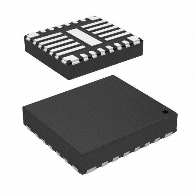


 工商网监
湘ICP备2023018690号
工商网监
湘ICP备2023018690号
