MSP430F471x3, MSP430F471x6, MSP430F471x7
MIXED SIGNAL MICROCONTROLLER
SLAS626C -- OCTOBER 2008 -- REVISED MARCH 2011
D Low Supply-Voltage Range: 1.8 V to 3.6 V
D Ultralow Power Consumption
D
D
D
D
D
D
D
D
D
D
D
D
D
D
D
-- Active Mode: 350 A at 1 MHz, 2.2 V
-- Standby Mode: 1.1 A
-- Off Mode (RAM Retention): 0.2 A
Five Power-Saving Modes
Wake-Up From Standby Mode in Less
Than 6 s
16-Bit RISC Architecture,
62.5-ns Instruction Cycle Time
Three-Channel Internal DMA
Three, Six or Seven 16-Bit Sigma-Delta
Analog-to-Digital (A/D) Converters With
Differential PGA Inputs
16-Bit Timer_B With Three
Capture/Compare-With-Shadow Registers
16-Bit Timer_A With Three
Capture/Compare Registers
On-Chip Comparator
Four Universal Serial Communication
Interface (USCI) Modules
-- USCI_A0 and USCI_A1
-- Enhanced UART Supporting
Auto-Baudrate Detection
-- IrDA Encoder and Decoder
-- Synchronous SPI
-- USCI_B0 and USCI_B1
-- I2C
-- Synchronous SPI
Integrated LCD Driver With Contrast
Control for Up to 160 Segments
Basic Timer With Real-Time Clock Feature
32-Bit Hardware Multiplier
Brownout Detector
Supply Voltage Supervisor/Monitor With
Programmable Level Detection
Serial Onboard Programming,
No External Programming Voltage Needed
Programmable Code Protection by Security
Fuse
D Bootstrap Loader
D On-Chip Emulation Module
D Family Members Include
D
D
D
MSP430F47163: 92KB Flash, 4KB RAM
3 Sigma-Delta ADCs
MSP430F47173: 92KB Flash, 8KB RAM
3 Sigma-Delta ADCs
MSP430F47183: 116KB Flash, 8KB RAM
3 Sigma-Delta ADCs
MSP430F47193: 120KB Flash, 4KB RAM
3 Sigma-Delta ADCs
MSP430F47126: 56KB Flash, 4KB RAM
6 Sigma-Delta ADCs
MSP430F47166: 92KB Flash, 4KB RAM
6 Sigma-Delta ADCs
MSP430F47176: 92KB Flash, 8KB RAM
6 Sigma-Delta ADCs
MSP430F47186: 116KB Flash, 8KB RAM
6 Sigma-Delta ADCs
MSP430F47196: 120KB Flash, 4KB RAM
6 Sigma-Delta ADCs
MSP430F47127: 56KB Flash, 4KB RAM
7 Sigma-Delta ADCs
MSP430F47167: 92KB Flash, 4KB RAM
7 Sigma-Delta ADCs
MSP430F47177: 92KB Flash, 8KB RAM
7 Sigma-Delta ADCs
MSP430F47187: 116KB Flash, 8KB RAM
7 Sigma-Delta ADCs
MSP430F47197: 120KB Flash, 4KB RAM
7 Sigma-Delta ADCs
Available in a 100-Pin Plastic Quad
Flatpack (QFP) Package
For Complete Module Descriptions, See the
MSP430x4xx Family User’s Guide,
Literature Number SLAU056
For E-Meter Reference Design and
Software, See Implementation of a
Three-Phase Electronic Watt-Hour Meter
using the MSP430F471xx, Literature
Number SLAA409
This integrated circuit can be damaged by ESD. Texas Instruments recommends that all integrated circuits be handled with
appropriate precautions. Failure to observe proper handling and installation procedures can cause damage. ESD damage can range
from subtle performance degradation to complete device failure. Precision integrated circuits may be more susceptible to damage
because very small parametric changes could cause the device not to meet its published specifications. These devices have limited
built-in ESD protection.
Please be aware that an important notice concerning availability, standard warranty, and use in critical applications of
Texas Instruments semiconductor products and disclaimers thereto appears at the end of this data sheet.
Copyright 2011, Texas Instruments Incorporated
PRODUCTION DATA information is current as of publication date.
Products conform to specifications per the terms of Texas Instruments
standard warranty. Production processing does not necessarily include
testing of all parameters.
POST OFFICE BOX 655303
DALLAS, TEXAS 75265
1
�MSP430F471x3, MSP430F471x6, MSP430F471x7
MIXED SIGNAL MICROCONTROLLER
SLAS626C -- OCTOBER 2008 -- REVISED MARCH 2011
description
The Texas Instruments MSP430 family of ultralow-power microcontrollers consists of several devices featuring
different sets of peripherals targeted for various applications. The architecture, combined with five low-power
modes, is optimized to achieve extended battery life in portable measurement applications. The devices feature
a powerful 16-bit RISC CPU, 16-bit registers, and constant generators that contribute to maximum code
efficiency. The digitally controlled oscillator (DCO) allows wake-up from low-power modes to active mode in less
than 6s.
The MSP430F471xx series are microcontroller configurations targeted to single-phase and poly-phase
electricity meters with three, six, or seven 16-bit sigma-delta A/D converters. Each channel has a differential
input pair and programmable input gain. Also integrated are two 16-bit timers, four universal serial
communication interfaces (USCI), DMA, 68 I/O pins, and a liquid crystal driver (LCD) with integrated contrast
control.
AVAILABLE OPTIONS{
TA
PACKAGED DEVICES}
PLASTIC 100-PIN QFP (PZ)
MSP430F47127IPZ
MSP430F47167IPZ
MSP430F47177IPZ
MSP430F47187IPZ
MSP430F47197IPZ
--40C to 85C
MSP430F47126IPZ
MSP430F47166IPZ
MSP430F47176IPZ
MSP430F47186IPZ
MSP430F47196IPZ
MSP430F47163IPZ
MSP430F47173IPZ
MSP430F47183IPZ
MSP430F47193IPZ
†
For the most current package and ordering information, see the
Package Option Addendum at the end of this document, or see the
TI web site at www.ti.com.
‡ Package drawings, thermal data, and symbolization are available at
www.ti.com/packaging.
DEVELOPMENT TOOL SUPPORT
All MSP430 microcontrollers include an Embedded Emulation Module (EEM) allowing advanced debugging
and programming through easy to use development tools. Recommended hardware options include the
following:
D Debugging and Programming Interface
--
MSP-FET430UIF (USB)
--
MSP-FET430PIF (Parallel Port)
D Debugging and Programming Interface with Target Board
--
MSP-FET430U100
D Stand-Alone Target Board
--
MSP-TS430PZ100
D Production Programmer
--
2
MSP-GANG430
POST OFFICE BOX 655303
DALLAS, TEXAS 75265
�MSP430F471x3, MSP430F471x6, MSP430F471x7
MIXED SIGNAL MICROCONTROLLER
SLAS626C -- OCTOBER 2008 -- REVISED MARCH 2011
functional block diagram, MSP430F471x7
XIN XOUT
XT2IN XT2OUT
2
2
Oscillators
FLL+
DVCC1/2
DVSS1/2
AVCC
AVSS
P1.x/P2.x
2x8
ACLK
SMCLK
MCLK
16MHz
CPU
incl. 16
Registers
Flash
RAM
120kB
116kB
92kB
92kB
56kB
4kB
8kB
4kB
8kB
4kB
SD16_A
(w/o BUF)
7
Sigma-Delta A/D
Converter
P3.x/P4.x
P5.x
3x8
P7.x/P8.x
P9.x/P10.x
3x8+1x4
Ports P1/P2
Comparator
_A
Ports
Ports
P3/P4
P7/P8
2x8 I/O
P5
P9/P10
Interrupt
capability &
3x8 I/O with 4x8/2x16 I/O
pull--up/down pull--up/down pull--up/down
Resistors
Resistors
Resistors
MAB
DMA
Controller
MDB
3 Channels
EEM
(L: 8 + 2)
Brownout
Protection
JTAG
Interface
SVS/SVM
Hardware
Multiplier
(32x32)
MPY,
MPYS,
MAC,
MACS
Watchdog
WDT+
15/16--Bit
Timer_A3
3 CC
Registers
Timer_B3
3 CC
Registers,
Shadow
Reg
Basic Timer
&
Real--Time
Clock
LCD_A
160
Segments
1,2,3,4 Mux
USCI_A0
(UART/LIN,
IrDA, SPI)
USCI_A1
(UART/LIN,
IrDA, SPI)
USCI_B0
(SPI, I2C)
USCI_B1
(SPI, I2C)
P3.x/P4.x
P5.x
3x8
P7.x/P8.x
P9.x/P10.x
3x8+1x4
RST/NMI
functional block diagram, MSP430F471x6
XIN XOUT
XT2IN XT2OUT
2
2
Oscillators
FLL+
DVCC1/2
ACLK
SMCLK
Flash
RAM
120kB
120kB
116kB
116kB
92kB
92kB
92kB
92kB
56kB
4kB
4kB
8kB
8kB
4kB
4kB
8kB
8kB
4kB
AVSS
P1.x/P2.x
SD16_A
(w/o BUF)
6
Sigma-Delta A/D
Converter
Ports P1/P2
Comparator
_A
Ports
P3/P4
P5
Ports
P7/P8
P9/P10
2x8 I/O
Interrupt
capability &
3x8 I/O with 4x8/2x16 I/O
pull--up/down pull--up/down pull--up/down
Resistors
Resistors
Resistors
MAB
DMA
Controller
MDB
3 Channels
EEM
(L: 8 + 2)
JTAG
Interface
AVCC
2x8
MCLK
16MHz
CPU
incl. 16
Registers
DVSS1/2
Brownout
Protection
SVS/SVM
Hardware
Multiplier
(32x32)
MPY,
MPYS,
MAC,
MACS
Watchdog
WDT+
15/16--Bit
Timer_A3
3 CC
Registers
Timer_B3
3 CC
Registers,
Shadow
Reg
Basic Timer
&
Real--Time
Clock
LCD_A
160
Segments
1,2,3,4 Mux
USCI_A0
(UART/LIN,
IrDA, SPI)
USCI_A1
(UART/LIN,
IrDA, SPI)
USCI_B0
(SPI, I2C)
USCI_B1
(SPI, I2C)
RST/NMI
POST OFFICE BOX 655303
DALLAS, TEXAS 75265
3
�MSP430F471x3, MSP430F471x6, MSP430F471x7
MIXED SIGNAL MICROCONTROLLER
SLAS626C -- OCTOBER 2008 -- REVISED MARCH 2011
functional block diagram, MSP430F471x3
XIN XOUT
XT2IN XT2OUT
2
2
Oscillators
FLL+
DVCC1/2
ACLK
SMCLK
Flash
RAM
120kB
116kB
92kB
92kB
4kB
8kB
4kB
8kB
AVSS
P1.x/P2.x
SD16_A
(w/o BUF)
3
Sigma-Delta A/D
Converter
P7.x/P8.x
P9.x/P10.x
3x8+1x4
Ports P1/P2
Comparator
_A
Ports
Ports
P3/P4
P7/P8
2x8 I/O
P5
P9/P10
Interrupt
capability &
3x8 I/O with 4x8/2x16 I/O
pull--up/down pull--up/down pull--up/down
Resistors
Resistors
Resistors
DMA
Controller
MDB
3 Channels
Brownout
Protection
SVS/SVM
Hardware
Multiplier
(32x32)
MPY,
MPYS,
MAC,
MACS
Watchdog
WDT+
15/16--Bit
Timer_A3
3 CC
Registers
Timer_B3
3 CC
Registers,
Shadow
Reg
Basic Timer
&
Real--Time
Clock
RST/NMI
4
P3.x/P4.x
P5.x
3x8
MAB
EEM
(L: 8 + 2)
JTAG
Interface
AVCC
2x8
MCLK
16MHz
CPU
incl. 16
Registers
DVSS1/2
POST OFFICE BOX 655303
DALLAS, TEXAS 75265
LCD_A
160
Segments
1,2,3,4 Mux
USCI_A0
(UART/LIN,
IrDA, SPI)
USCI_A1
(UART/LIN,
IrDA, SPI)
USCI_B0
(SPI, I2C)
USCI_B1
(SPI, I2C)
�MSP430F471x3, MSP430F471x6, MSP430F471x7
MIXED SIGNAL MICROCONTROLLER
SLAS626C -- OCTOBER 2008 -- REVISED MARCH 2011
pin designation, MSP430F471x7IPZ
1
2
3
4
5
6
7
8
9
10
11
12
13
14
15
16
17
18
19
20
21
22
23
24
25
MSP430F471x7IPZ
75
74
73
72
71
70
69
68
67
66
65
64
63
62
61
60
59
58
57
56
55
54
53
52
51
P3.0/UCB0STE/UCA0CLK
P3.1/UCB0SIMO/UCB0SDA
P3.2/UCB0SOMI/UCB0SCL
P3.3/UCB0CLK/UCA0STE
P3.4/TA2/S39
P3.5/TB0/S38
P3.6/TB1/S37
P3.7/TB2/S36
DVSS2
XOUT
XIN
DVCC2
LCDCAP/R33
P5.7/R23
P5.6/LCDREF/R13
P5.5/R03
P5.4/COM3
P5.3/COM2
P5.2/COM1
P5.1/COM0
P5.0/SVSIN
P4.0/CAOUT/S35
P4.1/DMAE0/S34
P4.2/S33
P4.3/S32
P9.4/S7
P9.3/S8
P9.2/S9
P9.1/S10
P9.0/S11
P8.7/S12
P8.6/S13
P8.5/S14
P8.4/S15
P8.3/S16
P8.2/S17
P8.1/S18
P8.0/S19
P7.7/S20
P7.6/S21
P7.5/S22
P7.4/S23
P7.3/S24
P7.2/S25
P7.1/S26
P7.0/S27
P4.7/S28
P4.6/S29
P4.5/S30
P4.4/S31
26
27
28
29
30
31
32
33
34
35
36
37
38
39
40
41
42
43
44
45
46
47
48
49
50
A0.0+†
A0.0-- †
A1.0+†
A1.0-- †
A2.0+†
A2.0-- †
AVSS
AVCC
VREF
A3.0+†
A3.0-- †
A4.0+†
A4.0-- †
A5.0+†
A5.0-- †
A6.0+†
A6.0-- †
AVSS
P10.3/S0
P10.2/S1
P10.1/S2
P10.0/S3
P9.7/S4
P9.6/S5
P9.5/S6
100
99
98
97
96
95
94
93
92
91
90
89
88
87
86
85
84
83
82
81
80
79
78
77
76
RST/NMI
TCK
TMS
TDI/TCLK
TDO/TDI
DVSS1
XT2IN
XT2OUT
DVCC1
P1.0/TA0
P1.1/TA0/MCLK
P1.2/TA1
P1.3/TBOUTH/SVSOUT
P1.4/TBCLK/SMCLK
P1.5/TACLK/ACLK
P1.6/UCA1TXD/UCA1SIMO
P1.7/UCA1RXD/UCA1SOMI
P2.0/UCB1STE/UCA1CLK
P2.1/UCB1SIMO/UCB1SDA
P2.2/UCB1SOMI/UCB1SCL
P2.3/UCB1CLK/UCA1STE
P2.4/UCA0TXD/UCA0SIMO
P2.5/UCA0RXD/UCA0SOMI
P2.6/CA0
P2.7/CA1
PZ PACKAGE
(TOP VIEW)
†
It is recommended to short unused analog input pairs and connect them to analog ground (AVSS).
POST OFFICE BOX 655303
DALLAS, TEXAS 75265
5
�MSP430F471x3, MSP430F471x6, MSP430F471x7
MIXED SIGNAL MICROCONTROLLER
SLAS626C -- OCTOBER 2008 -- REVISED MARCH 2011
pin designation, MSP430F471x6IPZ
1
2
3
4
5
6
7
8
9
10
11
12
13
14
15
16
17
18
19
20
21
22
23
24
25
MSP430F471x6IPZ
75
74
73
72
71
70
69
68
67
66
65
64
63
62
61
60
59
58
57
56
55
54
53
52
51
P9.4/S7
P9.3/S8
P9.2/S9
P9.1/S10
P9.0/S11
P8.7/S12
P8.6/S13
P8.5/S14
P8.4/S15
P8.3/S16
P8.2/S17
P8.1/S18
P8.0/S19
P7.7/S20
P7.6/S21
P7.5/S22
P7.4/S23
P7.3/S24
P7.2/S25
P7.1/S26
P7.0/S27
P4.7/S28
P4.6/S29
P4.5/S30
P4.4/S31
26
27
28
29
30
31
32
33
34
35
36
37
38
39
40
41
42
43
44
45
46
47
48
49
50
A0.0+†
A0.0-- †
A1.0+†
A1.0-- †
A2.0+†
A2.0-- †
AVSS
AVCC
VREF
A3.0+†
A3.0-- †
A4.0+†
A4.0-- †
A5.0+†
A5.0-- †
NC‡
NC‡
AVSS
P10.3/S0
P10.2/S1
P10.1/S2
P10.0/S3
P9.7/S4
P9.6/S5
P9.5/S6
100
99
98
97
96
95
94
93
92
91
90
89
88
87
86
85
84
83
82
81
80
79
78
77
76
RST/NMI
TCK
TMS
TDI/TCLK
TDO/TDI
DVSS1
XT2IN
XT2OUT
DVCC1
P1.0/TA0
P1.1/TA0/MCLK
P1.2/TA1
P1.3/TBOUTH/SVSOUT
P1.4/TBCLK/SMCLK
P1.5/TACLK/ACLK
P1.6/UCA1TXD/UCA1SIMO
P1.7/UCA1RXD/UCA1SOMI
P2.0/UCB1STE/UCA1CLK
P2.1/UCB1SIMO/UCB1SDA
P2.2/UCB1SOMI/UCB1SCL
P2.3/UCB1CLK/UCA1STE
P2.4/UCA0TXD/UCA0SIMO
P2.5/UCA0RXD/UCA0SOMI
P2.6/CA0
P2.7/CA1
PZ PACKAGE
(TOP VIEW)
†
‡
6
It is recommended to short unused analog input pairs and connect them to analog ground (AVSS).
Connect pin to analog ground (AVSS).
POST OFFICE BOX 655303
DALLAS, TEXAS 75265
P3.0/UCB0STE/UCA0CLK
P3.1/UCB0SIMO/UCB0SDA
P3.2/UCB0SOMI/UCB0SCL
P3.3/UCB0CLK/UCA0STE
P3.4/TA2/S39
P3.5/TB0/S38
P3.6/TB1/S37
P3.7/TB2/S36
DVSS2
XOUT
XIN
DVCC2
LCDCAP/R33
P5.7/R23
P5.6/LCDREF/R13
P5.5/R03
P5.4/COM3
P5.3/COM2
P5.2/COM1
P5.1/COM0
P5.0/SVSIN
P4.0/CAOUT/S35
P4.1/DMAE0/S34
P4.2/S33
P4.3/S32
�MSP430F471x3, MSP430F471x6, MSP430F471x7
MIXED SIGNAL MICROCONTROLLER
SLAS626C -- OCTOBER 2008 -- REVISED MARCH 2011
pin designation, MSP430F471x3IPZ
1
2
3
4
5
6
7
8
9
10
11
12
13
14
15
16
17
18
19
20
21
22
23
24
25
MSP430F471x3IPZ
75
74
73
72
71
70
69
68
67
66
65
64
63
62
61
60
59
58
57
56
55
54
53
52
51
P3.0/UCB0STE/UCA0CLK
P3.1/UCB0SIMO/UCB0SDA
P3.2/UCB0SOMI/UCB0SCL
P3.3/UCB0CLK/UCA0STE
P3.4/TA2/S39
P3.5/TB0/S38
P3.6/TB1/S37
P3.7/TB2/S36
DVSS2
XOUT
XIN
DVCC2
LCDCAP/R33
P5.7/R23
P5.6/LCDREF/R13
P5.5/R03
P5.4/COM3
P5.3/COM2
P5.2/COM1
P5.1/COM0
P5.0/SVSIN
P4.0/CAOUT/S35
P4.1/DMAE0/S34
P4.2/S33
P4.3/S32
P9.4/S7
P9.3/S8
P9.2/S9
P9.1/S10
P9.0/S11
P8.7/S12
P8.6/S13
P8.5/S14
P8.4/S15
P8.3/S16
P8.2/S17
P8.1/S18
P8.0/S19
P7.7/S20
P7.6/S21
P7.5/S22
P7.4/S23
P7.3/S24
P7.2/S25
P7.1/S26
P7.0/S27
P4.7/S28
P4.6/S29
P4.5/S30
P4.4/S31
26
27
28
29
30
31
32
33
34
35
36
37
38
39
40
41
42
43
44
45
46
47
48
49
50
A0.0+†
A0.0-- †
A1.0+†
A1.0-- †
A2.0+†
A2.0-- †
AVSS
AVCC
VREF
NC‡
NC‡
NC‡
NC‡
NC‡
NC‡
NC‡
NC‡
AVSS
P10.3/S0
P10.2/S1
P10.1/S2
P10.0/S3
P9.7/S4
P9.6/S5
P9.5/S6
100
99
98
97
96
95
94
93
92
91
90
89
88
87
86
85
84
83
82
81
80
79
78
77
76
RST/NMI
TCK
TMS
TDI/TCLK
TDO/TDI
DVSS1
XT2IN
XT2OUT
DVCC1
P1.0/TA0
P1.1/TA0/MCLK
P1.2/TA1
P1.3/TBOUTH/SVSOUT
P1.4/TBCLK/SMCLK
P1.5/TACLK/ACLK
P1.6/UCA1TXD/UCA1SIMO
P1.7/UCA1RXD/UCA1SOMI
P2.0/UCB1STE/UCA1CLK
P2.1/UCB1SIMO/UCB1SDA
P2.2/UCB1SOMI/UCB1SCL
P2.3/UCB1CLK/UCA1STE
P2.4/UCA0TXD/UCA0SIMO
P2.5/UCA0RXD/UCA0SOMI
P2.6/CA0
P2.7/CA1
PZ PACKAGE
(TOP VIEW)
†
‡
It is recommended to short unused analog input pairs and connect them to analog ground (AVSS).
Connect pin to analog ground (AVSS).
POST OFFICE BOX 655303
DALLAS, TEXAS 75265
7
�MSP430F471x3, MSP430F471x6, MSP430F471x7
MIXED SIGNAL MICROCONTROLLER
SLAS626C -- OCTOBER 2008 -- REVISED MARCH 2011
Terminal Functions
TERMINAL
NAME
NO.
I/O
DESCRIPTION
A0.0+
1
I
SD16_A positive analog input A0.0 (see Note 1)
A0.0--
2
I
SD16_A negative analog input A0.0 (see Note 1)
A1.0+
3
I
SD16_A positive analog input A1.0 (see Note 1)
A1.0--
4
I
SD16_A negative analog input A1.0 (see Note 1)
A2.0+
5
I
SD16_A positive analog input A2.0 (see Note 1)
A2.0--
6
I
SD16_A negative analog input A2.0 (see Note 1)
AVSS
7
Analog supply voltage, negative terminal.
AVCC
8
Analog supply voltage, positive terminal. Must not power up prior to DVCC1/DVCC2.
VREF
9
I/O
A3.0+
(MSP430F471x6/7 only)
10
I
SD16_A positive analog input A3.0 (see Note 1) -Not connected in MSP430F471x3, connect pin to analog ground (AVSS).
A3.0-(MSP430F471x6/7 only)
11
I
SD16_A negative analog input A3.0 (see Note 1) -Not connected in MSP430F471x3, connect pin to analog ground (AVSS).
A4.0+
(MSP430F471x6/7 only)
12
I
SD16_A positive analog input A4.0 (see Note 1) -Not connected in MSP430F471x3, connect pin to analog ground (AVSS).
A4.0-(MSP430F471x6/7 only)
13
I
SD16_A negative analog input A4.0 (see Note 1) -Not connected in MSP430F471x3, connect pin to analog ground (AVSS).
A5.0+
(MSP430F471x6/7 only)
14
I
SD16_A positive analog input A5.0 (see Note 1) -Not connected in MSP430F471x3, connect pin to analog ground (AVSS).
A5.0-(MSP430F471x6/7 only)
15
I
SD16_A negative analog input A5.0 (see Note 1) -Not connected in MSP430F471x3, connect pin to analog ground (AVSS).
A6.0+
(MSP430F471x7 only)
16
I
SD16_A positive analog input A6.0 (see Note 1) -Not connected in MSP430F471x6, connect pin to analog ground (AVSS).
A6.0-(MSP430F471x7 only)
17
I
SD16_A negative analog input A6.0 (see Note 1) -Not connected in MSP430F471x6, connect pin to analog ground (AVSS).
AVSS
18
P10.3/S0
19
I/O
General-purpose digital I/O / LCD segment output 0
P10.2/S1
20
I/O
General-purpose digital I/O / LCD segment output 1
P10.1/S2
21
I/O
General-purpose digital I/O / LCD segment output 2
P10.0/S3
22
I/O
General-purpose digital I/O / LCD segment output 3
P9.7/S4
23
I/O
General-purpose digital I/O / LCD segment output 4
P9.6/S5
24
I/O
General-purpose digital I/O / LCD segment output 5
P9.5/S6
25
I/O
General-purpose digital I/O / LCD segment output 6
P9.4/S7
26
I/O
General-purpose digital I/O / LCD segment output 7
P9.3/S8
27
I/O
General-purpose digital I/O / LCD segment output 8
P9.2/S9
28
I/O
General-purpose digital I/O / LCD segment output 9
P9.1/S10
29
I/O
General-purpose digital I/O / LCD segment output 10
P9.0/S11
30
I/O
General-purpose digital I/O / LCD segment output 11
P8.7/S12
31
I/O
General-purpose digital I/O / LCD segment output 12
P8.6/S13
32
I/O
General-purpose digital I/O / LCD segment output 13
P8.5/S14
33
I/O
General-purpose digital I/O / LCD segment output 14
P8.4/S15
34
I/O
General-purpose digital I/O / LCD segment output 15
P8.3/S16
35
I/O
General-purpose digital I/O / LCD segment output 16
P8.2/S17
36
I/O
General-purpose digital I/O / LCD segment output 17
P8.1/S18
37
I/O
General-purpose digital I/O / LCD segment output 18
Input for an external reference voltage /
internal reference voltage output (can be used as mid-voltage)
Analog supply voltage, negative terminal.
NOTES: 1. It is recommended to short unused analog input pairs and connect them to analog ground.
8
POST OFFICE BOX 655303
DALLAS, TEXAS 75265
�MSP430F471x3, MSP430F471x6, MSP430F471x7
MIXED SIGNAL MICROCONTROLLER
SLAS626C -- OCTOBER 2008 -- REVISED MARCH 2011
Terminal Functions (continued)
TERMINAL
NAME
NO.
I/O
DESCRIPTION
P8.0/S19
38
I/O
General-purpose digital I/O / LCD segment output 19
P7.7/S20
39
I/O
General-purpose digital I/O / LCD segment output 20
P7.6/S21
40
I/O
General-purpose digital I/O / LCD segment output 21
P7.5/S22
41
I/O
General-purpose digital I/O / LCD segment output 22
P7.4/S23
42
I/O
General-purpose digital I/O / LCD segment output 23
P7.3/S24
43
I/O
General-purpose digital I/O / LCD segment output 24
P7.2/S25
44
I/O
General-purpose digital I/O / LCD segment output 25
P7.1/S26
45
I/O
General-purpose digital I/O / LCD segment output 26
P7.0/S27
46
I/O
General-purpose digital I/O / LCD segment output 27
P4.7/S28
47
I/O
General-purpose digital I/O / LCD segment output 28
P4.6/S29
48
I/O
General-purpose digital I/O / LCD segment output 29
P4.5/S30
49
I/O
General-purpose digital I/O / LCD segment output 30
P4.4/S31
50
I/O
General-purpose digital I/O / LCD segment output 31
P4.3/S32
51
I/O
General-purpose digital I/O / LCD segment output 32
P4.2/S33
52
I/O
General-purpose digital I/O / LCD segment output 33
P4.1/DMAE0/S34
53
I/O
General-purpose digital I/O / DMA Channel 0 external trigger / LCD segment output 34
P4.0/CAOUT/S35
54
I/O
General-purpose digital I/O / Comparator_A output / LCD segment output 35
P5.0/SVSIN
55
I/O
General-purpose digital I/O / analog input to supply voltage supervisor
P5.1/COM0
56
I/O
General-purpose digital I/O / common output, COM0--3 are used for LCD backplanes.
P5.2/COM1
57
I/O
General-purpose digital I/O / common output, COM0--3 are used for LCD backplanes.
P5.3/COM2
58
I/O
General-purpose digital I/O / common output, COM0--3 are used for LCD backplanes.
P5.4/COM3
59
I/O
General-purpose digital I/O / common output, COM0--3 are used for LCD backplanes.
P5.5/R03
60
I/O
General-purpose digital I/O / Input port of lowest analog LCD level (V5)
P5.6/LCDREF/R13
61
I/O
General-purpose digital I/O / External reference voltage input for regulated LCD voltage / Input port
of third most positive analog LCD level (V4 or V3)
P5.7/R23
62
I/O
General-purpose digital I/O / Input port of second most positive analog LCD level (V2)
LCDCAP/R33
63
I
DVCC2
64
XIN
65
I
Input port for crystal oscillator XT1. Standard or watch crystals can be connected.
XOUT
66
O
Output terminal of crystal oscillator XT1
DVSS2
67
P3.7/TB2/S36
68
I/O
General-purpose digital I/O / Timer_B3 CCR2. Capture: CCI2A/CCI2B input, compare: Out2 output
/ LCD segment output 36
P3.6/TB1/S37
69
I/O
General-purpose digital I/O / Timer_B3 CCR1. Capture: CCI1A/CCI1B input, compare: Out1 output
/ LCD segment output 37
P3.5/TB0/S38
70
I/O
General-purpose digital I/O / Timer_B3 CCR0. Capture: CCI0A/CCI0B input, compare: Out0 output
/ LCD segment output 38
P3.4/TA2/S39
71
I/O
General-purpose digital I/O / Timer_A Capture: CCI2A input, compare: Out2 output
/ LCD segment output 39
P3.3/
UCB0CLK/UCA0STE
72
I/O
General-purpose digital I/O /
USCI_B0 clock input/output / USCI_A0 slave transmit enable
P3.2/
UCB0SOMI/UCB0SCL
73
I/O
General-purpose digital I/O /
USCI_B0 slave out/master in in SPI mode, SCL I2C clock in I2C mode
P3.1/
UCB0SIMO/UCB0SDA
74
I/O
General-purpose digital I/O /
USCI_B0 slave in/master out in SPI mode, SDA I2C data in I2C mode
LCD Capacitor connection / Input/output port of most positive analog LCD level (V1)
Digital supply voltage, positive terminal.
Digital supply voltage, negative terminal.
POST OFFICE BOX 655303
DALLAS, TEXAS 75265
9
�MSP430F471x3, MSP430F471x6, MSP430F471x7
MIXED SIGNAL MICROCONTROLLER
SLAS626C -- OCTOBER 2008 -- REVISED MARCH 2011
Terminal Functions (continued)
TERMINAL
NAME
I/O
NO.
DESCRIPTION
I/O
DESCRIPTION
P3.0/
UCB0STE/UCA0CLK
75
I/O
General-purpose digital I/O /
USCI_B0 slave transmit enable / USCI_A0 clock input/output
P2.7/CA1
76
I/O
General-purpose digital I/O / Comparator_A input
P2.6/CA0
77
I/O
General-purpose digital I/O / Comparator_A input
P2.5/
UCA0RXD/UCA0SOMI
78
I/O
General-purpose digital I/O / USCI_A0 receive data input in UART mode, slave out/master in in SPI
mode
P2.4/
UCA0TXD/UCA0SIMO
79
I/O
General-purpose digital I/O / USCI_A0 transmit data output in UART mode, slave in/master out in
SPI mode
P2.3/
UCB1CLK/UCA1STE
80
I/O
General-purpose digital I/O /
USCI_B1 clock input/output / USCI_A1 slave transmit enable
P2.2/
UCB1SOMI/UCB1SCL
81
I/O
General-purpose digital I/O /
USCI_B1 slave out/master in in SPI mode, SCL I2C clock in I2C mode
P2.1/
UCB1SIMO/UCB1SDA
82
I/O
General-purpose digital I/O /
USCI_B1 slave in/master out in SPI mode, SDA I2C data in I2C mode
P2.0/
UCB1STE/UCA1CLK
83
I/O
General-purpose digital I/O /
USCI_B1 slave transmit enable / USCI_A1 clock input/output
P1.7/
UCA1RXD/UCA1SOMI
84
I/O
General-purpose digital I/O /
USCI_A1 receive data input in UART mode, slave out/master in in SPI mode
P1.6/
UCA1TXD/UCA1SIMO
85
I/O
General-purpose digital I/O /
USCI_A1 transmit data output in UART mode, slave in/master out in SPI mode
P1.5/TACLK/ACLK
86
I/O
General-purpose digital I/O / Timer_A, clock signal TACLK input /
ACLK output (divided by 1, 2, 4, or 8)
P1.4/TBCLK/SMCLK
87
I/O
General-purpose digital I/O / input clock TBCLK—Timer_B3 /
submain system clock SMCLK output
P1.3/TBOUTH/SVSOUT
88
I/O
General-purpose digital I/O / switch all PWM digital output ports to high impedance—Timer_B3 TB0
to TB2 / SVS: output of SVS comparator
P1.2/TA1
89
I/O
General-purpose digital I/O / Timer_A, Capture: CCI1A input, compare: Out1 output
P1.1/TA0/MCLK
90
I/O
General-purpose digital I/O / Timer_A. Capture: CCI0B input / MCLK output.
Note: TA0 is only an input on this pin / BSL receive
P1.0/TA0
91
I/O
General-purpose digital I/O / Timer_A. Capture: CCI0A input, compare: Out0 output / BSL transmit
DVCC1
92
XT2OUT
93
O
Output terminal of crystal oscillator XT2
XT2IN
94
I
Input port for crystal oscillator XT2. Only standard crystals can be connected.
DVSS1
95
TDO/TDI
96
I/O
TDI/TCLK
97
I
Test data input or test clock input. The device protection fuse is connected to TDI/TCLK.
TMS
98
I
Test mode select. TMS is used as an input port for device programming and test.
TCK
99
I
Test clock. TCK is the clock input port for device programming and test.
RST/NMI
100
I
Reset input or nonmaskable interrupt input port
10
Digital supply voltage, positive terminal.
Digital supply voltage, negative terminal.
Test data output port. TDO/TDI data output or programming data input terminal
POST OFFICE BOX 655303
DALLAS, TEXAS 75265
�MSP430F471x3, MSP430F471x6, MSP430F471x7
MIXED SIGNAL MICROCONTROLLER
SLAS626C -- OCTOBER 2008 -- REVISED MARCH 2011
short-form description
CPU
The MSP430 CPU has a 16-bit RISC architecture
that is highly transparent to the application. All
operations, other than program-flow instructions,
are performed as register operations in
conjunction with seven addressing modes for
source operand and four addressing modes for
destination operand.
Program Counter
PC/R0
Stack Pointer
SP/R1
Status Register
Constant Generator
The CPU is integrated with 16 registers that
provide reduced instruction execution time. The
register-to-register operation execution time is
one cycle of the CPU clock.
Four of the registers, R0 to R3, are dedicated as
program counter, stack pointer, status register,
and constant generator, respectively. The
remaining registers are general-purpose
registers.
Peripherals are connected to the CPU using data,
address, and control buses and can be handled
with all instructions.
instruction set
The instruction set consists of 51 instructions with
three formats and seven address modes. Each
instruction can operate on word and byte data.
Table 1 shows examples of the three types of
instruction formats; Table 2 shows the address
modes.
SR/CG1/R2
CG2/R3
General-Purpose Register
R4
General-Purpose Register
R5
General-Purpose Register
R6
General-Purpose Register
R7
General-Purpose Register
R8
General-Purpose Register
R9
General-Purpose Register
R10
General-Purpose Register
R11
General-Purpose Register
R12
General-Purpose Register
R13
General-Purpose Register
R14
General-Purpose Register
R15
Table 1. Instruction Word Formats
Dual operands, source-destination
e.g., ADD R4,R5
R4 + R5 ------> R5
Single operands, destination only
e.g., CALL R8
PC ---->(TOS), R8----> PC
Relative jump, un/conditional
e.g., JNE
Jump-on-equal bit = 0
Table 2. Address Mode Descriptions
ADDRESS MODE
Register
Indexed
Symbolic (PC relative)
Absolute
Indirect
S D
D
D
D
D
D
D
D
D
D
SYNTAX
EXAMPLE
OPERATION
MOV Rs,Rd
MOV R10,R11
R10 ----> R11
MOV X(Rn),Y(Rm)
MOV 2(R5),6(R6)
M(2+R5)----> M(6+R6)
MOV EDE,TONI
M(EDE) ----> M(TONI)
MOV &MEM,&TCDAT
M(MEM) ----> M(TCDAT)
MOV @Rn,Y(Rm)
MOV @R10,Tab(R6)
M(R10) ----> M(Tab+R6)
Indirect
autoincrement
D
MOV @Rn+,Rm
MOV @R10+,R11
M(R10) ----> R11
R10 + 2----> R10
Immediate
D
MOV #X,TONI
MOV #45,TONI
#45 ----> M(TONI)
NOTE: S = source, D = destination
POST OFFICE BOX 655303
DALLAS, TEXAS 75265
11
�MSP430F471x3, MSP430F471x6, MSP430F471x7
MIXED SIGNAL MICROCONTROLLER
SLAS626C -- OCTOBER 2008 -- REVISED MARCH 2011
operating modes
The MSP430 has one active mode and five software-selectable low-power modes of operation. An interrupt
event can wake up the device from any of the five low-power modes, service the request, and restore back to
the low-power mode on return from the interrupt program.
The following six operating modes can be configured by software:
D Active mode AM
--
All clocks are active
D Low-power mode 0 (LPM0)
--
CPU is disabled
--
ACLK and SMCLK remain active. MCLK is disabled.
--
FLL+ loop control remains active
D Low-power mode 1 (LPM1)
--
CPU is disabled
--
FLL+ loop control is disabled
--
ACLK and SMCLK remain active. MCLK is disabled.
D Low-power mode 2 (LPM2)
--
CPU is disabled
--
MCLK and FLL+ loop control and DCOCLK are disabled
--
DCO’s dc generator remains enabled
--
ACLK remains active
D Low-power mode 3 (LPM3)
--
CPU is disabled
--
MCLK, FLL+ loop control, and DCOCLK are disabled
--
DCO’s dc generator is disabled
--
ACLK remains active
D Low-power mode 4 (LPM4)
12
--
CPU is disabled
--
ACLK is disabled
--
MCLK, FLL+ loop control, and DCOCLK are disabled
--
DCO’s dc generator is disabled
--
Crystal oscillator is stopped
POST OFFICE BOX 655303
DALLAS, TEXAS 75265
�MSP430F471x3, MSP430F471x6, MSP430F471x7
MIXED SIGNAL MICROCONTROLLER
SLAS626C -- OCTOBER 2008 -- REVISED MARCH 2011
interrupt vector addresses
The interrupt vectors and the power-up starting address are located in the address range 0FFFFh to 0FFC0h.
The vector contains the 16-bit address of the appropriate interrupt-handler instruction sequence. If the reset
vector (at 0FFFEh) contains 0FFFFh (e.g., flash is not programmed) the CPU enters LPM4 after power-up.
INTERRUPT SOURCE
INTERRUPT FLAG
SYSTEM INTERRUPT
WORD
ADDRESS
PRIORITY
Power-Up
External Reset
Watchdog
Flash Memory
PC Out-of-Range (see Note 4)
PORIFG
RSTIFG
WDTIFG
KEYV
(see Note 1)
Reset
0FFFEh
31, highest
NMI
Oscillator Fault
Flash Memory Access Violation
NMIIFG (see Notes 1 and 3)
OFIFG (see Notes 1 and 3)
ACCVIFG (see Notes 1 and 3)
(Non)maskable
(Non)maskable
(Non)maskable
0FFFCh
30
Timer_B3
TBCCR0 CCIFG (see Note 2)
Maskable
0FFFAh
29
Timer_B3
TBCCR1 to TBCCR2 CCIFGs
TBIFG (see Notes 1 and 2)
Maskable
0FFF8h
28
Comparator_A
CAIFG
Maskable
0FFF6h
27
Watchdog Timer
WDTIFG
Maskable
0FFF4h
26
USCI_A0/B0 Receive
USCI_B0 I2C Status
UCA0RXIFG, UCB0RXIFG
(see Notes 1 and 5)
Maskable
0FFF2h
25
USCI_A0/B0 Transmit
USCI_B0 I2C Receive/Transmit
UCA0TXIFG, UCB0TXIFG
(see Notes 1 and 6)
Maskable
0FFF0h
24
SD16_A
SD16CCTLx SD16OVIFG, SD16CCTLx SD16IFG
(see Notes 1 and 2)
Maskable
0FFEEh
23
Timer_A3
TACCR0 CCIFG (see Note 2)
Maskable
0FFECh
22
Timer_A3
TACCR1 and TACCR2 CCIFGs,
TAIFG (see Notes 1 and 2)
Maskable
0FFEAh
21
I/O Port P1 (Eight Flags)
P1IFG.0 to P1IFG.7 (see Notes 1 and 2)
Maskable
0FFE8h
20
USCI_A1/B1 Receive
USCI_B1 I2C Status
UCA1RXIFG, UCB1RXIFG
(see Notes 1 and 5)
Maskable
0FFE6h
19
USCI_A1/B1 Transmit
USCI_B1 I2C Receive/Transmit
UCA1TXIFG, UCB1TXIFG
(see Notes 1 and 6)
Maskable
0FFE4h
18
I/O Port P2 (Eight Flags)
P2IFG.0 to P2IFG.7 (see Notes 1 and 2)
Maskable
0FFE2h
17
Basic Timer1/RTC
BTIFG
Maskable
0FFE0h
16
DMA
DMA0IFG, DMA1IFG, DMA2IFG
(see Notes 1 and 2)
Maskable
0FFDEh
15
Reserved
Reserved (see Note 8)
0FFDCh to
14 to
0FFC0h
0, lowest
NOTES: 1. Multiple source flags
2. Interrupt flags are located in the module.
3. (Non)maskable: the individual interrupt-enable bit can disable an interrupt event, but the general-interrupt enable can not disable
it.
4. A reset is generated if the CPU tries to fetch instructions from within the module register memory address range (0h to 01FFh) or
from within unused address ranges.
5. USCI_B in SPI mode: UCBxRXIFG. USCI_B in I2C mode: UCALIFG, UCNACKIFG, ICSTTIFG, UCSTPIFG
6. USCI_B in SPI mode: UCBxTXIFG. USCI_B in I2C mode: UCBxRXIFG, UCBxTXIFG
7. The address 0x0FFBE is used as bootstrap loader security key (BSLSKEY).
A 0x0AA55 at this location disables the BSL completely.
A zero disables the erasure of the flash if an invalid password is supplied.
8. The interrupt vectors at addresses 0FFDCh to 0FFC0h are not used in this device and can be used for regular program code if
necessary.
POST OFFICE BOX 655303
DALLAS, TEXAS 75265
13
�MSP430F471x3, MSP430F471x6, MSP430F471x7
MIXED SIGNAL MICROCONTROLLER
SLAS626C -- OCTOBER 2008 -- REVISED MARCH 2011
special function registers
The MSP430 special function registers (SFR) are located in the lowest address space and are organized as
byte mode registers. SFRs should be accessed with byte instructions.
interrupt enable 1 and 2
Address
7
6
00h
4
ACCVIE
rw--0
3
2
1
0
NMIIE
OFIE
WDTIE
rw--0
rw--0
rw--0
WDTIE
Watchdog timer interrupt enable. Inactive if watchdog mode is selected. Active if watchdog
timer is configured in interval timer mode.
OFIE
Oscillator fault enable
NMIIE
(Non)maskable interrupt enable
ACCVIE
Flash access violation interrupt enable
Address
01h
14
5
7
6
5
4
3
2
1
0
BTIE
UCB0TXIE
UCB0RXIE
UCA0TXIE
UCA0RXIE
rw--0
rw--0
rw--0
rw--0
rw--0
UCA0RXIE
USCI_A0 receive interrupt enable
UCA0TXIE
USCI_A0 transmit interrupt enable
UCB0RXIE
USCI_B0 receive interrupt enable
UCB0TXIE
USCI_B0 transmit interrupt enable
BTIE
Basic timer interrupt enable
POST OFFICE BOX 655303
DALLAS, TEXAS 75265
�MSP430F471x3, MSP430F471x6, MSP430F471x7
MIXED SIGNAL MICROCONTROLLER
SLAS626C -- OCTOBER 2008 -- REVISED MARCH 2011
interrupt flag register 1 and 2
Address
7
6
5
02h
4
3
2
1
0
NMIIFG
RSTIFG
PORIFG
OFIFG
WDTIFG
rw--0
rw--(0)
rw--(1)
rw--1
rw--(0)
WDTIFG
Set on watchdog timer overflow or security key violation.
Reset on VCC power-up or a reset condition at RST/NMI pin in reset mode.
OFIFG
Flag set on oscillator fault
RSTIFG
External reset interrupt flag. Set on a reset condition at RST/NMI pin in reset mode. Reset
on VCC power-up
PORIFG
Power-on interrupt flag. Set on VCC power-up.
NMIIFG
Set via RST/NMI-pin
Address
7
03h
UCA0RXIFG
6
5
3
2
1
0
BTIFG
UCB0
TXIFG
UCB0
RXIFG
UCA0
TXIFG
UCA0
RXIFG
rw--0
rw--1
rw--0
rw--1
rw--0
USCI_A0 receive interrupt flag
UCA0TXIFG
USCI_A0 transmit interrupt flag
UCB0RXIFG
USCI_B0 receive interrupt flag
UCB0TXIFG
USCI_B0 transmit interrupt flag
BTIFG
Basic Timer1 interrupt flag
Legend
4
rw:
rw-0,1:
rw-(0,1):
Bit can be read and written.
Bit can be read and written. It is Reset or Set by PUC.
Bit can be read and written. It is Reset or Set by POR.
SFR bit is not present in device
POST OFFICE BOX 655303
DALLAS, TEXAS 75265
15
�MSP430F471x3, MSP430F471x6, MSP430F471x7
MIXED SIGNAL MICROCONTROLLER
SLAS626C -- OCTOBER 2008 -- REVISED MARCH 2011
memory organization
MSP430F47126/
MSP430F47127
MSP430F47163/
MSP430F47166/
MSP430F47167
MSP430F47173/
MSP430F47176/
MSP430F47177
MSP430F47183/
MSP430F47186/
MSP430F47187
MSP430F47193/
MSP430F47196/
MSP430F47197
Size
Flash
Flash
56KB
0FFFFh -- 0FFC0h
0FFFFh--002100h
92KB
0FFFFh -- 0FFC0h
018FFFh-002100h
92KB
0FFFFh -- 0FFC0h
019FFFh-003100h
116KB
0FFFFh -- 0FFC0h
01FFFFh-003100h
120KB
0FFFFh -- 0FFC0h
01FFFFh-002100h
Size
4KB
020FFh--01100h
4KB
020FFh--01100h
8KB
030FFh--01100h
8KB
030FFh--01100h
4KB
020FFh--01100h
Extended
Size
2KB
020FFh--01900h
2KB
020FFh--01900h
6KB
030FFh--01900h
6KB
030FFh--01900h
2KB
020FFh--01900h
Mirrored
Size
2KB
018FFh--01100h
2KB
018FFh--01100h
2KB
018FFh--01100h
2KB
018FFh--01100h
2KB
018FFh--01100h
Information memory
Size
Flash
256 Byte
010FFh--01000h
256 Byte
010FFh--01000h
256 Byte
010FFh--01000h
256 Byte
010FFh--01000h
256 Byte
010FFh--01000h
Boot memory
Size
ROM
1KB
0FFFh--0C00h
1KB
0FFFh--0C00h
1KB
0FFFh -- 0C00h
1KB
0FFFh--0C00h
1KB
0FFFh--0C00h
Size
2KB
09FFh--0200h
2KB
09FFh--0200h
2KB
09FFh--0200h
2KB
09FFh--0200h
2KB
09FFh--0200h
16-bit
8-bit
8-bit SFR
01FFh--0100h
0FFh--010h
0Fh--00h
01FFh--0100h
0FFh--010h
0Fh--00h
01FFh--0100h
0FFh--010h
0Fh--00h
01FFh--0100h
0FFh--010h
0Fh--00h
01FFh--0100h
0FFh--010h
0Fh--00h
Memory
Main: interrupt vector
Main: code memory
RAM (Total)
RAM
(mirrored at
018FFh -- 01100h)
Peripherals
bootstrap loader (BSL)
The MSP430 bootstrap loader (BSL) enables users to program the flash memory or RAM using a UART serial
interface. Access to the MSP430 memory via the BSL is protected by user-defined password. For complete
description of the features of the BSL and its implementation, see the MSP430 Memory Programming User’s
Guide, literature number SLAU265.
BSL FUNCTION
PZ PACKAGE PINS
Data Transmit
91 - P1.0
Data Receive
90 - P1.1
flash memory
The flash memory can be programmed via the JTAG port, the bootstrap loader, or in-system by the CPU. The
CPU can perform single-byte and single-word writes to the flash memory. Features of the flash memory include:
D Flash memory has n segments of main memory and four segments of information memory (A to D) of
64 bytes each. Each segment in main memory is 512 bytes in size.
D Segments 0 to n may be erased in one step, or each segment may be individually erased.
D Segments A to D can be erased individually, or as a group with segments 0 to n.
Segments A to D are also called information memory.
D Segment A might contain calibration data. After reset segment A is protected against programming or
erasing. It can be unlocked but care should be taken not to erase this segment if the calibration data is
required.
D Flash content integrity check with marginal read modes.
16
POST OFFICE BOX 655303
DALLAS, TEXAS 75265
�MSP430F471x3, MSP430F471x6, MSP430F471x7
MIXED SIGNAL MICROCONTROLLER
SLAS626C -- OCTOBER 2008 -- REVISED MARCH 2011
peripherals
Peripherals are connected to the CPU through data, address, and control buses and can be handled using all
instructions. For complete module descriptions, see the MSP430x4xx Family User’s Guide, literature number
SLAU056.
oscillator and system clock
The clock system is supported by the FLL+ module that includes support for a 32768-Hz watch crystal oscillator,
an internal digitally-controlled oscillator (DCO) and an 8-MHz high-frequency crystal oscillator (XT1) plus a
16-MHz high-frequency crystal oscillator (XT2). The FLL+ clock module is designed to meet the requirements
of both low system cost and low power consumption. The FLL+ features a digital frequency locked loop (FLL)
hardware that, in conjunction with a digital modulator, stabilizes the DCO frequency to a programmable multiple
of the watch crystal frequency. The internal DCO provides a fast turn-on clock source and stabilizes in less than
6 s. The FLL+ module provides the following clock signals:
D
D
D
D
Auxiliary clock (ACLK), sourced from a 32768-Hz watch crystal or a high-frequency crystal
Main clock (MCLK), the system clock used by the CPU
Sub-Main clock (SMCLK), the sub-system clock used by the peripheral modules
ACLK/n, the buffered output of ACLK, ACLK/2, ACLK/4, or ACLK/8
brownout, supply voltage supervisor (SVS)
The brownout circuit is implemented to provide the proper internal reset signal to the device during power on
and power off. The SVS circuitry detects if the supply voltage drops below a user selectable level and supports
both supply voltage supervision (the device is automatically reset) and supply voltage monitoring (SVM, the
device is not automatically reset).
The CPU begins code execution after the brownout circuit releases the device reset. However, VCC may not
have ramped to VCC(min) at that time. The user must insure the default FLL+ settings are not changed until VCC
reaches VCC(min). If desired, the SVS circuit can be used to determine when VCC reaches VCC(min).
digital I/O
There are nine 8-bit I/O ports implemented—ports P1 through P5 and P7 through P10.
D
D
D
D
D
D
All individual I/O bits are independently programmable.
Any combination of input, output, and interrupt conditions is possible.
Edge-selectable interrupt input capability for all the eight bits of ports P1 and P2.
Read/write access to port-control registers is supported by all instructions.
Ports P7/P8 and P9/P10 can be accessed word-wise as ports PA and PB respectively.
Each I/O has an individually programmable pullup/pulldown resistor.
Note: Only four bits of port P10 (P10.0 to P10.3) are available on external pins, but all control and data bits for port P10 are implemented.
POST OFFICE BOX 655303
DALLAS, TEXAS 75265
17
�MSP430F471x3, MSP430F471x6, MSP430F471x7
MIXED SIGNAL MICROCONTROLLER
SLAS626C -- OCTOBER 2008 -- REVISED MARCH 2011
DMA controller
The DMA controller allows movement of data from one memory address to another without CPU intervention.
For example, the DMA controller can be used to move data from a USCI module to RAM. Using the DMA
controller can increase the throughput of peripheral modules. The DMA controller reduces system power
consumption by allowing the CPU to remain in sleep mode without having to awaken to move data to or from
a peripheral.
DMA TRIGGER SELECT DMAXTSELX
DESCRIPTION
0000
DMAREQ bit (software trigger)
0001
TACCR2 CCIFG bit
0010
TBCCR2 CCIFG bit
0011
UCA0RXIFG bit
0100
UCA0TXIFG bit
0101
N/A
0110
SD16IFG bit
0111
TACCR0 CCIFG bit
1000
TBCCR0 CCIFG bit
1001
UCA1RXIFG bit
1010
UCA1TXIFG bit
1011
Multiplier ready
1100
UCB0RXIFG bit
1101
UCB0TXIFG bit
1110
1111
DMA0IFG bit triggers DMA channel 1
DMA1IFG bit triggers DMA channel 2
DMA2IFG bit triggers DMA channel 0
External trigger DMAE0
hardware multiplier
The multiplication operation is supported by a dedicated peripheral module. The module performs operations
with 32-bit, 24-bit, 16-bit and 8-bit operands. The module is capable of supporting signed and unsigned
multiplication as well as signed and unsigned multiply and accumulate operations.
watchdog timer (WDT+)
The primary function of the WDT+ module is to perform a controlled system restart after a software problem
occurs. If the selected time interval expires, a system reset is generated. If the watchdog function is not needed
in an application, the module can be configured as an interval timer and can generate interrupts at selected time
intervals.
Basic Timer1 and Real-Time Clock (RTC)
The Basic Timer1 has two independent 8-bit timers that can be cascaded to form a 16-bit timer/counter. Both
timers can be read and written by software. The Basic Timer1 is extended to provide an integrated real-time
clock (RTC). An internal calendar compensates for months with less than 31 days and includes leap year
correction.
18
POST OFFICE BOX 655303
DALLAS, TEXAS 75265
�MSP430F471x3, MSP430F471x6, MSP430F471x7
MIXED SIGNAL MICROCONTROLLER
SLAS626C -- OCTOBER 2008 -- REVISED MARCH 2011
universal serial communication interfaces (USCIs) (USCI_A0, USCI_B0, USCI_A1, USCI_B1)
The USCI module is used for serial data communication. The USCI module supports synchronous
communication protocols such as SPI (3-pin or 4-pin) and I2C and asynchronous communication protocols such
as UART, enhanced UART with automatic baudrate detection (LIN), and IrDA.
USCI_A0 and USCI_A1 provides support for SPI (3-pin or 4-pin), UART, enhanced UART, and IrDA.
USCI_B0 and USCI_B1 provides support for SPI (3-pin or 4-pin) and I2C.
Timer_A3
Timer_A3 is a 16-bit timer/counter with three capture/compare registers. Timer_A3 can support multiple
capture/compares, PWM outputs, and interval timing. Timer_A3 also has extensive interrupt capabilities.
Interrupts may be generated from the counter on overflow conditions and from each of the capture/compare
registers.
TIMER_A3 SIGNAL CONNECTIONS
INPUT PIN
NUMBER
DEVICE INPUT
SIGNAL
MODULE INPUT
NAME
86 - P1.5
TACLK
TACLK
ACLK
ACLK
SMCLK
SMCLK
86 - P1.5
TACLK
INCLK
91 - P1.0
TA0
CCI0A
90 - P1.1
TA0
CCI0B
DVSS
GND
89 - P1.2
71 - P3.4
DVCC
VCC
TA1
CCI1A
CAOUT (internal)
CCI1B
DVSS
GND
DVCC
VCC
TA2
CCI2A
ACLK (internal)
CCI2B
DVSS
GND
DVCC
VCC
POST OFFICE BOX 655303
MODULE BLOCK
MODULE OUTPUT
SIGNAL
Timer
NA
OUTPUT PIN
NUMBER
91 - P1.0
CCR0
TA0
89 - P1.2
CCR1
TA1
71 - P3.4
CCR2
DALLAS, TEXAS 75265
TA2
19
�MSP430F471x3, MSP430F471x6, MSP430F471x7
MIXED SIGNAL MICROCONTROLLER
SLAS626C -- OCTOBER 2008 -- REVISED MARCH 2011
Timer_B3
Timer_B3 is a 16-bit timer/counter with three capture/compare registers. Timer_B3 can support multiple
capture/compares, PWM outputs, and interval timing. Timer_B3 also has extensive interrupt capabilities.
Interrupts may be generated from the counter on overflow conditions and from each of the capture/compare
registers.
TIMER_B3 SIGNAL CONNECTIONS
INPUT PIN
NUMBER
DEVICE INPUT
SIGNAL
MODULE INPUT
NAME
87 - P1.4
TBCLK
TBCLK
ACLK
ACLK
SMCLK
SMCLK
87 - P1.4
TBCLK
INCLK
70 -- P3.5
TB0
CCI0A
TB0
CCI0B
DVSS
GND
70 -- P3.5
DVCC
VCC
69 - P3.6
TB1
CCI1A
69 - P3.6
TB1
CCI1B
DVSS
GND
68 - P3.7
68 - P3.7
DVCC
VCC
TB2
CCI2A
TB2
CCI2B
DVSS
GND
DVCC
VCC
MODULE BLOCK
MODULE OUTPUT
SIGNAL
Timer
NA
OUTPUT PIN
NUMBER
70 - P3.5
CCR0
TB0
69 - P3.6
CCR1
TB1
68 - P3.7
CCR2
TB2
Comparator_A
The primary function of the comparator_A module is to support precision slope analog-to-digital conversions,
battery-voltage supervision, and monitoring of external analog signals.
SD16_A
The SD16_A module integrates three (MSP430F471x3), six (MSP430F471x6) or seven (MSP430F471x7)
independent 16-bit sigma-delta A/D converters. Each channel is designed with a fully differential analog input
pair and programmable gain amplifier input stage. In addition to external analog inputs, an internal VCC sense
and temperature sensor are also available.
LCD driver with regulated charge pump
The LCD_A driver generates the segment and common signals required to drive an LCD display. The LCD_A
controller has dedicated data memory to hold segment drive information. Common and segment signals are
generated as defined by the mode. Static, 2-MUX, 3-MUX, and 4-MUX LCDs are supported by this peripheral.
The module can provide a LCD voltage independent of the supply voltage via an integrated charge pump.
Furthermore it is possible to control the level of the LCD voltage and thus contrast in software.
20
POST OFFICE BOX 655303
DALLAS, TEXAS 75265
�MSP430F471x3, MSP430F471x6, MSP430F471x7
MIXED SIGNAL MICROCONTROLLER
SLAS626C -- OCTOBER 2008 -- REVISED MARCH 2011
embedded emulation module (EEM)
All MSP430F471x3, MSP430F471x6, and MSP430F471x7 devices have an EEM that supports real-time
in-system debugging. The implemented L version of the EEM has the following features:
D
D
D
D
D
D
D
Eight hardware triggers on memory address or data bus
Two hardware triggers on write accesses to CPU register
Eight combinational triggers to combine any of the 10 above hardware triggers
Trigger sequencer
CPU break reaction on combinational triggers for breakpoints
State storage to trace internal buses
Clock control on module level
POST OFFICE BOX 655303
DALLAS, TEXAS 75265
21
�MSP430F471x3, MSP430F471x6, MSP430F471x7
MIXED SIGNAL MICROCONTROLLER
SLAS626C -- OCTOBER 2008 -- REVISED MARCH 2011
peripheral file map
PERIPHERALS WITH WORD ACCESS
Watchdog
Watchdog timer control
WDTCTL
0120h
Flash_A
Flash control 4
Flash control 3
Flash control 2
FCTL4
FCTL3
FCTL2
01BEh
012Ch
012Ah
Flash control 1
FCTL1
0128h
Capture/compare register 2
TBCCR2
0196h
Capture/compare register 1
TBCCR1
0194h
Capture/compare register 0
TBCCR0
0192h
Timer_B register
TBR
0190h
Capture/compare control 2
TBCCTL2
0186h
Capture/compare control 1
TBCCTL1
0184h
Capture/compare control 0
TBCCTL0
0182h
Timer_B control
TBCTL
0180h
Timer_B interrupt vector
TBIV
011Eh
Capture/compare register 2
TACCR2
0176h
Capture/compare register 1
TACCR1
0174h
Capture/compare register 0
TACCR0
0172h
Timer_A register
TAR
0170h
Capture/compare control 2
TACCTL2
0166h
Capture/compare control 1
TACCTL1
0164h
Capture/compare control 0
TACCTL0
0162h
Timer_A control
TACTL
0160h
Timer_A interrupt vector
TAIV
012Eh
MPY32 control 0
MPY32CTL0
015Ch
64-bit result 3 -- most significant word
RES3
015Ah
64-bit result 2
RES2
0158h
64-bit result 1
RES1
0156h
64-bit result 0 -- least significant word
RES0
0154h
Second 32-bit operand, high word
OP2H
0152h
Second 32-bit operand, low word
OP2L
0150h
Multiply signed + accumulate/
32-bit operand1, high word
MACS32H
014Eh
Multiply signed + accumulate/
32-bit operand1, low word
MACS32L
014Ch
Multiply + accumulate/
32-bit operand1, high word
MAC32H
014Ah
Multiply + accumulate/
32-bit operand1, low word
MAC32L
0148h
Multiply signed/32-bit operand1, high word
MPYS32H
0146h
Multiply signed/32-bit operand1, low word
MPYS32L
0144h
Multiply unsigned/32-bit operand1, high word
MPY32H
0142h
Multiply unsigned/32-bit operand1, low word
MPY32L
0140h
Timer_B3
_
Timer_A3
_
32-bit Hardware
M l i li
Multiplier
22
POST OFFICE BOX 655303
DALLAS, TEXAS 75265
�MSP430F471x3, MSP430F471x6, MSP430F471x7
MIXED SIGNAL MICROCONTROLLER
SLAS626C -- OCTOBER 2008 -- REVISED MARCH 2011
peripheral file map (continued)
PERIPHERALS WITH WORD ACCESS (CONTINUED)
32-bit Hardware
Multiplier
Sum extend
SUMEXT
013Eh
Result high word
RESHI
013Ch
Result low word
RESLO
013Ah
Second operand
OP2
0138h
Multiply signed + accumulate/operand1
MACS
0136h
Multiply + accumulate/operand1
MAC
0134h
Multiply signed/operand1
MPYS
0132h
Multiply unsigned/operand1
MPY
0130h
USCI_B0
USCI_B0 I2C own address
(see also: Peripherals with Byte Ac- USCI_B0 I2C slave address
cess)
UCB0I2COA
016Ch
UCB0I2CSA
016Eh
USCI_B1
USCI_B1 I2C own address
(see also: Peripherals with Byte Ac- USCI_B1 I2C slave address
cess)
UCB1I2COA
017Ch
UCB1I2CSA
017Eh
SD16_A
_
General Control
(
(see
also:
l
PeripherP i h
Channel 0 Control
als with Byte Access))
Channel 1 Control
SD16CTL
0100h
SD16CCTL0
0102h
SD16CCTL1
0104h
Channel 2 Control
SD16CCTL2
0106h
Channel 3 Control
SD16CCTL3
0108h
Channel 4 Control
SD16CCTL4
010Ah
Channel 5 Control
SD16CCTL5
010Ch
Channel 6 Control
SD16CCTL6
010Eh
Channel 0 conversion memory
SD16MEM0
0110h
Channel 1 conversion memory
SD16MEM1
0112h
Channel 2 conversion memory
SD16MEM2
0114h
Channel 3 conversion memory
SD16MEM3
0116h
Channel 4 conversion memory
SD16MEM4
0118h
Channel 5 conversion memory
SD16MEM5
011Ah
Channel 6 conversion memory
SD16MEM6
011Ch
SD16 Interrupt vector word register
SD16IV
01AEh
Port PA resistor enable
PAREN
014h
Port PA selection
PASEL
03Eh
Port PA direction
PADIR
03Ch
Port PA output
PAOUT
03Ah
Port PA input
PAIN
038h
Port PB resistor enable
PBREN
016h
Port PB selection
PBSEL
00Eh
Port PB direction
PBDIR
00Ch
Port PB output
PBOUT
00Ah
Port PB input
PBIN
008h
Port PA
Port PB
POST OFFICE BOX 655303
DALLAS, TEXAS 75265
23
�MSP430F471x3, MSP430F471x6, MSP430F471x7
MIXED SIGNAL MICROCONTROLLER
SLAS626C -- OCTOBER 2008 -- REVISED MARCH 2011
peripheral file map (continued)
PERIPHERALS WITH WORD ACCESS (CONTINUED)
DMA
DMA Channel 0
DMA Channel 1
DMA Channel 2
24
DMA module control 0
DMACTL0
0122h
DMA module control 1
DMACTL1
0124h
DMA interrupt vector
DMAIV
0126h
DMA channel 0 control
DMA0CTL
01D0h
DMA channel 0 source address
DMA0SA
01D2h
DMA channel 0 destination address
DMA0DA
01D6h
DMA channel 0 transfer size
DMA0SZ
01DAh
DMA channel 1 control
DMA1CTL
01DCh
DMA channel 1 source address
DMA1SA
01DEh
DMA channel 1 destination address
DMA1DA
01E2h
DMA channel 1 transfer size
DMA1SZ
01E6h
DMA channel 2 control
DMA2CTL
01E8h
DMA channel 2 source address
DMA2SA
01EAh
DMA channel 2 destination address
DMA2DA
01EEh
DMA channel 2 transfer size
DMA2SZ
01F2h
POST OFFICE BOX 655303
DALLAS, TEXAS 75265
�MSP430F471x3, MSP430F471x6, MSP430F471x7
MIXED SIGNAL MICROCONTROLLER
SLAS626C -- OCTOBER 2008 -- REVISED MARCH 2011
peripheral file map (continued)
PERIPHERALS WITH BYTE ACCESS
SD16_A
(see also:
Peripherals with
Word Access)
LCD_A
Channel 0 Input Control
Channel 1 Input Control
Channel 2 Input Control
SD16INCTL0
SD16INCTL1
SD16INCTL2
0B0h
0B1h
0B2h
Channel 3 Input Control
Channel 4 Input Control
Channel 5 Input Control
Channel 6 Input Control
SD16INCTL3
SD16INCTL4
SD16INCTL5
SD16INCTL6
0B3h
0B4h
0B5h
0B6h
Reserved
Channel 0 preload
Channel 1 preload
Channel 2 preload
SD16PRE0
SD16PRE1
SD16PRE2
0B7h
0B8h
0B9h
0BAh
Channel 3 preload
Channel 4 preload
Channel 5 preload
Channel 6 preload
SD16PRE3
SD16PRE4
SD16PRE5
SD16PRE6
0BBh
0BCh
0BDh
0BEh
Reserved
SD16CONF1
0BFh
LCD Voltage Control 1
LCD Voltage Control 0
LCD Voltage Port Control 1
LCDAVCTL1
LCDAVCTL0
LCDAPCTL1
0AFh
0AEh
0ADh
LCD Voltage Port Control 0
LCD memory 20
:
LCD memory 16
LCDAPCTL0
LCDM20
:
LCDM16
0ACh
0A4h
:
0A0h
LCD memory 15
:
LCD memory 1
LCD control and mode
LCDM15
:
LCDM1
LCDACTL
09Fh
:
091h
090h
POST OFFICE BOX 655303
DALLAS, TEXAS 75265
25
�MSP430F471x3, MSP430F471x6, MSP430F471x7
MIXED SIGNAL MICROCONTROLLER
SLAS626C -- OCTOBER 2008 -- REVISED MARCH 2011
peripheral file map (continued)
PERIPHERALS WITH BYTE ACCESS (CONTINUED)
USCI_A0
USCI_A0 transmit buffer
USCI_A0 receive buffer
USCI_A0 status
USCI_A0 modulation control
USCI_A0 baud rate control 1
USCI_A0 baud rate control 0
USCI_A0 control 1
USCI_A0 control 0
USCI_A0 IrDA receive control
USCI_A0 IrDA transmit control
USCI_A0 auto baud rate control
UCA0TXBUF
UCA0RXBUF
UCA0STAT
UCA0MCTL
UCA0BR1
UCA0BR0
UCA0CTL1
UCA0CTL0
UCA0IRRCTL
UCA0IRTCTL
UCA0ABCTL
067h
066h
065h
064h
063h
062h
061h
060h
05Fh
05Eh
05Dh
USCI_B0
USCI_B0 transmit buffer
USCI_B0 receive buffer
USCI_B0 status
USCI_B1 I2C interrupt enable
USCI_B0 bit rate control 1
USCI_B0 bit rate control 0
USCI_B0 control 1
USCI_B0 control 0
UCB0TXBUF
UCB0RXBUF
UCB0STAT
UCB0I2CIE
UCB0BR1
UCB0BR0
UCB0CTL1
UCB0CTL0
06Fh
06Eh
06Dh
06Ch
06Bh
06Ah
069h
068h
USCI_A1
USCI_A1 transmit buffer
USCI_A1 receive buffer
USCI_A1 status
USCI_A1 modulation control
USCI_A1 baud rate control 1
USCI_A1 baud rate control 0
USCI_A1 control 1
USCI_A1 control 0
USCI_A1 IrDA receive control
USCI_A1 IrDA transmit control
USCI_A1 auto baud rate control
USCI_A1 interrupt flag
USCI_A1 interrupt enable
UCA1TXBUF
UCA1RXBUF
UCA1STAT
UCA1MCTL
UCA1BR1
UCA1BR0
UCA1CTL1
UCA1CTL0
UCA1IRRCTL
UCA1IRTCTL
UCA1ABCTL
UC1IFG
UC1IE
0D7h
0D6h
0D5h
0D4h
0D3h
0D2h
0D1h
0D0h
0CFh
0CEh
0CDh
007h
006h
USCI_B1
USCI_B1 transmit buffer
USCI_B1 receive buffer
USCI_B1 status
USCI_B1 I2C interrupt enable
USCI_B1 bit rate control 1
USCI_B1 bit rate control 0
USCI_B1 control 1
USCI_B1 control 0
USCI_A1 interrupt flag
USCI_A1 interrupt enable
UCB1TXBUF
UCB1RXBUF
UCB1STAT
UCB1I2CIE
UCB1BR1
UCB1BR0
UCB1CTL1
UCB1CTL0
UC1IFG
UC1IE
0DFh
0DEh
0DDh
0DCh
0DBh
0DAh
0D9h
0D8h
007h
006h
Comparator_A
p
_
Comparator_A port disable
CAPD
05Bh
Comparator_A control2
CACTL2
05Ah
Comparator_A control1
CACTL1
059h
SVS control register (Reset by brownout signal)
SVSCTL
056h
BrownOUT, SVS
26
POST OFFICE BOX 655303
DALLAS, TEXAS 75265
�MSP430F471x3, MSP430F471x6, MSP430F471x7
MIXED SIGNAL MICROCONTROLLER
SLAS626C -- OCTOBER 2008 -- REVISED MARCH 2011
peripheral file map (continued)
PERIPHERALS WITH BYTE ACCESS (CONTINUED)
FLL+ Clock
RTC
(Basic Timer 1)
Port P10
Port P9
Port P8
Port P7
FLL+ Control2
FLL_CTL2
055h
FLL+ Control1
FLL_CTL1
054h
FLL+ Control0
FLL_CTL0
053h
System clock frequency control
SCFQCTL
052h
System clock frequency integrator
SCFI1
051h
System clock frequency integrator
SCFI0
050h
Real Time Clock Year High Byte
RTCYEARH
04Fh
Real Time Clock Year Low Byte
RTCYEARL
04Eh
Real Time Clock Month
RTCMON
04Dh
Real Time Clock Day of Month
RTCDAY
04Ch
Basic Timer1 Counter 2
BTCNT2
047h
Basic Timer1 Counter 1
BTCNT1
046h
Real Time Counter 4
(Real Time Clock Day of Week)
RTCNT4
(RTCDOW)
045h
Real Time Counter 3
(Real Time Clock Hour)
RTCNT3
(RTCHOUR)
044h
Real Time Counter 2
(Real Time Clock Minute)
RTCNT2
(RTCMIN)
043h
Real Time Counter 1
(Real Time Clock Second)
RTCNT1
(RTCSEC)
042h
Real Time Clock Control
RTCCTL
041h
Basic Timer1 Control
BTCTL
040h
Port P10 resistor enable
P10REN
017h
Port P10 selection
P10SEL
00Fh
Port P10 direction
P10DIR
00Dh
Port P10 output
P10OUT
00Bh
Port P10 input
P10IN
009h
Port P9 resistor enable
P9REN
016h
Port P9 selection
P9SEL
00Eh
Port P9 direction
P9DIR
00Ch
Port P9 output
P9OUT
00Ah
Port P9 input
P9IN
008h
Port P8 resistor enable
P8REN
015h
Port P8 selection
P8SEL
03Fh
Port P8 direction
P8DIR
03Dh
Port P8 output
P8OUT
03Bh
Port P8 input
P8IN
039h
Port P7 resistor enable
P7REN
014h
Port P7 selection
P7SEL
03Eh
Port P7 direction
P7DIR
03Ch
Port P7 output
P7OUT
03Ah
Port P7 input
P7IN
038h
POST OFFICE BOX 655303
DALLAS, TEXAS 75265
27
�MSP430F471x3, MSP430F471x6, MSP430F471x7
MIXED SIGNAL MICROCONTROLLER
SLAS626C -- OCTOBER 2008 -- REVISED MARCH 2011
peripheral file map (continued)
PERIPHERALS WITH BYTE ACCESS (CONTINUED)
Port P5
Port P4
Port P3
Port P2
Port P1
Special
p
Functions
28
Port P5 resistor enable
P5REN
012h
Port P5 selection
P5SEL
033h
Port P5 direction
P5DIR
032h
Port P5 output
P5OUT
031h
Port P5 input
P5IN
030h
Port P4 resistor enable
P4REN
011h
Port P4 selection
P4SEL
01Fh
Port P4 direction
P4DIR
01Eh
Port P4 output
P4OUT
01Dh
Port P4 input
P4IN
01Ch
Port P3 resistor enable
P3REN
010h
Port P3 selection
P3SEL
01Bh
Port P3 direction
P3DIR
01Ah
Port P3 output
P3OUT
019h
Port P3 input
P3IN
018h
Port P2 resistor enable
P2REN
02Fh
Port P2 selection
P2SEL
02Eh
Port P2 interrupt enable
P2IE
02Dh
Port P2 interrupt-edge select
P2IES
02Ch
Port P2 interrupt flag
P2IFG
02Bh
Port P2 direction
P2DIR
02Ah
Port P2 output
P2OUT
029h
Port P2 input
P2IN
028h
Port P1 resistor enable
P1REN
027h
Port P1 selection
P1SEL
026h
Port P1 interrupt enable
P1IE
025h
Port P1 interrupt-edge select
P1IES
024h
Port P1 interrupt flag
P1IFG
023h
Port P1 direction
P1DIR
022h
Port P1 output
P1OUT
021h
Port P1 input
P1IN
020h
SFR interrupt flag2
IFG2
003h
SFR interrupt flag1
IFG1
002h
SFR interrupt enable2
IE2
001h
SFR interrupt enable1
IE1
000h
POST OFFICE BOX 655303
DALLAS, TEXAS 75265
�MSP430F471x3, MSP430F471x6, MSP430F471x7
MIXED SIGNAL MICROCONTROLLER
SLAS626C -- OCTOBER 2008 -- REVISED MARCH 2011
absolute maximum ratings (see Note 1)
Voltage applied at VCC to VSS . . . . . . . . . . . . . . . . . . . . . . . . . . . . . . . . . . . . . . . . . . . . . . . . . . . . . . --0.3 V to 4.1 V
Voltage applied to any pin (see Note 2) . . . . . . . . . . . . . . . . . . . . . . . . . . . . . . . . . . . . . . . --0.3 V to VCC + 0.3 V
Diode current at any device terminal . . . . . . . . . . . . . . . . . . . . . . . . . . . . . . . . . . . . . . . . . . . . . . . . . . . . . . . 2 mA
Storage temperature, Tstg: Unprogrammed device (see Note 3) . . . . . . . . . . . . . . . . . . . . . . . --55C to 150C
Programmed device (see Note 3) . . . . . . . . . . . . . . . . . . . . . . . . . . --40C to 85C
NOTES: 1. Stresses beyond those listed under “absolute maximum ratings” may cause permanent damage to the device. These are stress
ratings only, and functional operation of the device at these or any other conditions beyond those indicated under “recommended
operating conditions” is not implied. Exposure to absolute-maximum-rated conditions for extended periods may affect device
reliability.
2. All voltages referenced to VSS. The JTAG fuse-blow voltage, VFB, is allowed to exceed the absolute maximum rating. The voltage
is applied to the TDI/TCLK pin when blowing the JTAG fuse.
3. Higher temperature may be applied during board soldering process according to the current JEDEC J--STD--020 specification with
peak reflow temperatures not higher than classified on the device label on the shipping boxes or reels.
POST OFFICE BOX 655303
DALLAS, TEXAS 75265
29
�MSP430F471x3, MSP430F471x6, MSP430F471x7
MIXED SIGNAL MICROCONTROLLER
SLAS626C -- OCTOBER 2008 -- REVISED MARCH 2011
recommended operating conditions
MIN
NOM
MAX
UNIT
Supply voltage during program execution,
VCC (AVCC = DVCC = VCC) (see Note 1)
1.8
3.6
V
Supply voltage during program execution, SVS enabled, PORON = 1,
VCC (AVCC = DVCC = VCC) (see Notes 1, 2)
2.0
3.6
V
Supply voltage during program/erase flash memory,
VCC (AVCC = DVCC = VCC) (see Note 1)
2.2
3.6
V
--40
85
C
VCC = 1.8 V,
Duty cycle = 50% 10%
dc
4.15
MHz
VCC = 2.2 V,
Duty cycle = 50% 10%
dc
7.5
MHz
VCC = 2.7 V,
Duty cycle = 50% 10%
dc
12
VCC 3.3 V,
Duty cycle = 50% 10%
dc
16
Supply voltage, VSS
0
Operating free-air temperature range, TA
Processor frequency fSYSTEM (Maximum MCLK frequency)
(see Notes 3, 4 and Figure 1)
V
MHz
NOTES: 1. It is recommended to power AVCC and DVCC from the same source. A maximum difference of 0.3 V between AVCC and DVCC can
be tolerated during power up and operation.
2. The minimum operating supply voltage is defined according to the trip point where POR is going active by decreasing supply voltage.
POR is going inactive when the supply voltage is raised above minimum supply voltage plus the hysteresis of the SVS circuitry.
3. The MSP430 CPU is clocked directly with MCLK.
Both the high and low phase of MCLK must not exceed the pulse width of the specified maximum frequency.
4. Modules might have a different maximum input clock specification. Refer to the specification of the respective module in this data
sheet.
Legend:
System Frequency --MHz
16 MHz
Supply voltage range,
during flash memory
programming
12 MHz
Supply voltage range,
during program execution
7.5 MHz
4.15 MHz
1.8 V
2.2 V
2.7 V
3.3 V
3.6 V
Supply Voltage --V
NOTE: Minimum processor frequency is defined by system clock. Flash program or erase operations require a minimum VCC of 2.2 V.
Figure 1. Operating Area
30
POST OFFICE BOX 655303
DALLAS, TEXAS 75265
�MSP430F471x3, MSP430F471x6, MSP430F471x7
MIXED SIGNAL MICROCONTROLLER
SLAS626C -- OCTOBER 2008 -- REVISED MARCH 2011
electrical characteristics over recommended operating free-air temperature (unless otherwise
noted)
supply current into AVCC + DVCC excluding external current
PARAMETER
TEST CONDITIONS
TYP
MAX
2.2 V
350
400
3V
500
560
2.2 V
45
70
3V
75
110
2.2 V
11
14
3V
17
22
TA = --40C
0.7
2.0
TA = 25C
0.8
2.0
2.0
3.5
TA = 85C
5.0
9.5
TA = --40C
1.1
3.0
1.2
3.0
2.5
4.0
TA = 85C
6.0
10.0
TA = --40C
3.5
5.5
TA = 25C
3.5
5.5
5.5
7.0
TA = 85C
11.0
17.0
TA = --40C
4.0
6.5
TA = 25C
4.0
6.5
6.0
8.0
TA = 85C
13.0
20.0
TA = --40C
0.1
1.0
TA = 25C
0.2
1.0
1.0
2.5
TA = 85C
4.5
8.5
TA = --40C
0.1
2.0
TA = 25C
0.2
2.0
1.5
3.0
5.0
9.0
Active mode, (see Note 1)
f((MCLK)) = f((SMCLK)) = 1 MHz,
f(ACLK) = 32768 Hz
XTS = 0, SELM = (0,1)
(Program executes from flash)
TA = --40C
40C to 85C
I(LPM0)
Low power mode, (LPM0)
Low-power
(see Notes 1, 4)
40C to 85C
TA = --40C
I(LPM2)
Low-power mode, (LPM2),
f(MCLK) = f (SMCLK) = 0 MHz,
MHz
f(ACLK) = 32768 Hz, SCG0 = 0 (see Notes 2, 4)
TA = --40C
40C to 85C
I(AM)
I(LPM3)
Low-power
Low
power mode
mode, (LPM3)
f(MCLK) = f(SMCLK) = 0 MHz,
f(ACLK) = 32768 Hz, SCG0 = 1
Basic Timer1 and RTC enabled , ACLK selected
LCD A enabled,
LCD_A
enabled LCDCPEN = 0:
(static mode , fLCD = f(ACLK)/32)
(see Notes
otes 2,, 3, and
a d 4))
TA = 60C
TA = 25C
TA = 60C
I(LPM3)
Low-power
Low
power mode
mode, (LPM3)
f(MCLK) = f(SMCLK) = 0 MHz,
f(ACLK) = 32768 Hz, SCG0 = 1
Basic Timer1 and RTC enabled , ACLK selected
LCD A enabled,
LCD_A
enabled LCDCPEN = 0:
(4-mux mode, fLCD = f(ACLK)/32)
(see Notes
otes 2,, 3, and
a d 4))
TA = 60C
TA = 60C
I(LPM4)
Low-power mode, (LPM4)
f(MCLK) = 0 MHz,
MHz f(SMCLK) = 0 MHz,
MHz
f(ACLK) = 0 Hz, SCG0 = 1 (see Notes 2 and 4)
TA = 60C
TA = 60C
TA = 85C
NOTES: 1.
2.
3.
4.
VCC
MIN
UNIT
A
A
22V
2.2
3V
22V
2.2
3V
22V
2.2
3V
A
A
A
A
A
A
A
A
A
A
A
A
A
A
A
A
Timer_A is clocked by f(DCOCLK) = f(DCO) = 1 MHz. All inputs are tied to 0 V or to VCC. Outputs do not source or sink any current.
All inputs are tied to 0 V or to VCC. Outputs do not source or sink any current.
The LPM3 currents are characterized with a Micro Crystal CC4V--T1A (9 pF) crystal and OSCCAPx = 01h.
Current for brownout included.
POST OFFICE BOX 655303
DALLAS, TEXAS 75265
31
�MSP430F471x3, MSP430F471x6, MSP430F471x7
MIXED SIGNAL MICROCONTROLLER
SLAS626C -- OCTOBER 2008 -- REVISED MARCH 2011
typical characteristics -- active mode supply current (into VCC)
11.0
fDCO = 16 MHz
10.0
fDCO = 12 MHz
7.0
6.0
fDCO = 8 MHz
5.0
4.0
3.0
2.0
fDCO = 1 MHz
1.0
0.0
1.5
2.0
2.5
3.0
3.5
4.0
Active Mode Current -- mA
Active Mode Current -- mA
9.0
8.0
TA = 85 C
6.0
TA = 25 C
5.0
4.0
3.0
VCC = 3 V
TA = 25 C
2.0
32
POST OFFICE BOX 655303
VCC = 2.2 V
1.0
0.0
0.0
VCC -- Supply Voltage -- V
Figure 2. Active Mode Current vs VCC, TA = 25C
TA = 85 C
4.0
8.0
12.0
16.0
fDCO -- DCO Frequency -- MHz
Figure 3. Active Mode Current vs DCO Frequency
DALLAS, TEXAS 75265
�MSP430F471x3, MSP430F471x6, MSP430F471x7
MIXED SIGNAL MICROCONTROLLER
SLAS626C -- OCTOBER 2008 -- REVISED MARCH 2011
electrical characteristics over recommended ranges of supply voltage and operating free-air
temperature (unless otherwise noted) (continued)
Schmitt-trigger inputs -- Ports P1 to P5, P7 to P10, RST/NMI, JTAG (TCK, TMS, TDI/TCLK, TDO/TDI)
PARAMETER
VIT+
VIT--
TEST CONDITIONS
Positive-going
P
iti
i input
i
t threshold
th h ld
voltage
Negative-going
N
ti
i input
i
t threshold
th h ld
voltage
Vhys
Input voltage hysteresis (VIT+ -VIT-- )
RPull
Pullup/pulldown resistor
(not RST/NMI and JTAG pins)
For pullup: VIN = VSS,
For pulldown: VIN = VCC
CI
Input capacitance
VIN = VSS or VCC
VCC
MIN
MAX
UNIT
0.45
0.75
VCC
2.2 V
1.00
1.65
3V
1.35
2.25
0.25
0.55
2.2 V
0.55
1.20
3V
0.75
1.65
2.2 V
0.2
1.0
3V
0.3
1.0
20
TYP
35
50
5
V
VCC
V
V
kΩ
pF
inputs -- Ports P1, P2
PARAMETER
t(int)
TEST CONDITIONS
Port P1, P2: P1.x to P2.x, external
trigger puls width to set interrupt flag
(see Note 1)
External interrupt timing
VCC
2.2 V/3 V
MIN
MAX
20
UNIT
ns
NOTES: 1. An external signal sets the interrupt flag every time the minimum interrupt puls width t(int) is met. It may be set even with trigger signals
shorter than t(int).
leakage current -- Ports P1 to P5, P7 to P10
PARAMETER
Ilkg(Px.x)
TEST CONDITIONS
High-impedance leakage current
See Notes 1 and 2
VCC
2.2 V/3 V
MIN
MAX
UNIT
50
nA
NOTES: 1. The leakage current is measured with VSS or VCC applied to the corresponding pin(s), unless otherwise noted.
2. The leakage of the digital port pins is measured individually. The port pin is selected for input and the pullup/pulldown resistor is
disabled.
POST OFFICE BOX 655303
DALLAS, TEXAS 75265
33
�MSP430F471x3, MSP430F471x6, MSP430F471x7
MIXED SIGNAL MICROCONTROLLER
SLAS626C -- OCTOBER 2008 -- REVISED MARCH 2011
electrical characteristics over recommended ranges of supply voltage and operating free-air
temperature (unless otherwise noted) (continued)
outputs -- Ports P1 to P5, P7 to P10
PARAMETER
VOH
VOL
High level output voltage
High-level
Low level output voltage
Low-level
VCC
MIN
I(OHmax) = --1.5 mA (see Note 1)
TEST CONDITIONS
2.2 V
VCC --0.25
MAX
VCC
UNIT
I(OHmax) = --6 mA (see Note 2)
2.2 V
VCC --0.6
VCC
I(OHmax) = --1.5 mA (see Note 1)
3V
VCC --0.25
VCC
I(OHmax) = --6 mA (see Note 2)
3V
VCC --0.6
VCC
I(OLmax) = 1.5 mA (see Note 1)
2.2 V
VSS
VSS+0.25
I(OLmax) = 6 mA (see Note 2)
2.2 V
VSS
VSS+0.6
I(OLmax) = 1.5 mA (see Note 1)
3V
VSS
VSS+0.25
I(OLmax) = 6 mA (see Note 2)
3V
VSS
VSS+0.6
V
V
NOTES: 1. The maximum total current, IOHmax and IOLmax, for all outputs combined, should not exceed 12 mA to hold the maximum
voltage drop specified.
2. The maximum total current, IOHmax and IOLmax, for all outputs combined, should not exceed 48 mA to hold the maximum
voltage drop specified.
output frequency -- Ports P1 to P5, P7 to P10
PARAMETER
fPx.y
Port output frequency (with load)
TEST CONDITIONS
P1.4/TBCLK/SMCLK,
CL = 20 pF
pF, RL = 1 kΩ against VCC/2
(see Notes 1 and 2)
MAX
UNIT
2.2 V
VCC
MIN
10
MHz
3V
12
MHz
P1.1/TA0/MCLK, P1.5/TACLK/ACLK,
2.2 V
12 MHz
fPort_CLK
Clock output frequency
P1 4/TBCLK/SMCLK
P1.4/TBCLK/SMCLK,
3V
16 MHz
CL = 20 pF (see Note 2)
NOTES: 1. Alternatively a resistive divider with 2 times 2 kΩ between VCC and VSS is used as load. The output is connected to the center tap
of the divider.
2. The output voltage reaches at least 10% and 90% VCC at the specified toggle frequency.
34
POST OFFICE BOX 655303
DALLAS, TEXAS 75265
�MSP430F471x3, MSP430F471x6, MSP430F471x7
MIXED SIGNAL MICROCONTROLLER
SLAS626C -- OCTOBER 2008 -- REVISED MARCH 2011
electrical characteristics over recommended ranges of supply voltage and operating free-air
temperature (unless otherwise noted) (continued)
typical characteristics -- outputs
TYPICAL LOW-LEVEL OUTPUT CURRENT
vs
LOW-LEVEL OUTPUT VOLTAGE
TYPICAL LOW-LEVEL OUTPUT CURRENT
vs
LOW-LEVEL OUTPUT VOLTAGE
50.0
VCC = 2.2 V
P1.6
25.0
I OL -- Typical Low-Level Output Current -- mA
I OL -- Typical Low-Level Output Current -- mA
30.0
TA = 25C
TA = 85C
20.0
15.0
10.0
5.0
0.0
0.0
0.5
1.0
1.5
2.0
VCC = 3 V
P1.6
40.0
TA = 85C
30.0
20.0
10.0
0.0
0.0
2.5
0.5
VOL -- Low-Level Output Voltage -- V
2.0
2.5
3.0
3.5
TYPICAL HIGH-LEVEL OUTPUT CURRENT
vs
HIGH-LEVEL OUTPUT VOLTAGE
0.0
0.0
VCC = 2.2 V
P1.6
I OH -- Typical High-Level Output Current -- mA
I OH -- Typical High-Level Output Current -- mA
1.5
Figure 5
TYPICAL HIGH-LEVEL OUTPUT CURRENT
vs
HIGH-LEVEL OUTPUT VOLTAGE
--5.0
--10.0
--15.0
--20.0
TA = 85C
--25.0
TA = 25C
0.5
1.0
VOL -- Low-Level Output Voltage -- V
Figure 4
--30.0
0.0
TA = 25C
1.0
1.5
2.0
2.5
VOH -- High-Level Output Voltage -- V
VCC = 3 V
P1.6
--10.0
--20.0
--30.0
--40.0
TA = 85C
--50.0
TA = 25C
--60.0
0.0
0.5
1.0
1.5
2.0
2.5
3.0
3.5
VOH -- High-Level Output Voltage -- V
Figure 6
Figure 7
NOTE: One output loaded at a time.
POST OFFICE BOX 655303
DALLAS, TEXAS 75265
35
�MSP430F471x3, MSP430F471x6, MSP430F471x7
MIXED SIGNAL MICROCONTROLLER
SLAS626C -- OCTOBER 2008 -- REVISED MARCH 2011
electrical characteristics over recommended ranges of supply voltage and operating free-air
temperature (unless otherwise noted) (continued)
POR/brownout reset (BOR) (see Notes 1 and 2)
PARAMETER
TEST CONDITIONS
VCC(start)
(See Figure 8)
dVCC/dt 3 V/s
V(B_IT--)
(See Figure 8 through Figure 10)
dVCC/dt 3 V/s
Vhys(B_IT--)
(See Figure 8)
dVCC/dt 3 V/s
td(BOR)
(See Figure 8)
t(reset)
Pulse length needed at RST/NMI pin
to accepted reset internally
VCC
MIN
TYP
MAX
0.7 V(B_IT--)
70
2.2 V/3 V
2
130
UNIT
V
1.71
V
180
mV
2000
s
s
NOTES: 1. The current consumption of the brownout module is already included in the ICC current consumption data.
The voltage level V(B_IT--) + Vhys(B_IT--) is 1.8 V.
2. During power up, the CPU begins code execution following a period of td(BOR) after VCC = V(B_IT--) + Vhys(B_IT--). The default FLL+
settings must not be changed until VCC VCC(min), where VCC(min) is the minimum supply voltage for the desired operating frequency.
See the MSP430x4xx Family User’s Guide (SLAU056) for more information on the brownout/SVS circuit.
VCC
Vhys(B_IT--)
V(B_IT--)
VCC(start)
1
0
t d(BOR)
Figure 8. POR/Brownout Reset (BOR) vs Supply Voltage
36
POST OFFICE BOX 655303
DALLAS, TEXAS 75265
�MSP430F471x3, MSP430F471x6, MSP430F471x7
MIXED SIGNAL MICROCONTROLLER
SLAS626C -- OCTOBER 2008 -- REVISED MARCH 2011
electrical characteristics over recommended ranges of supply voltage and operating free-air
temperature (unless otherwise noted) (continued)
typical characteristics -- POR/brownout reset (BOR)
VCC
3V
VCC(drop) -- V
2
VCC = 3 V
Typical Conditions
1.5
t pw
1
VCC(drop)
0.5
0
0.001
1
1000
1 ns
tpw -- Pulse Width -- s
1 ns
tpw -- Pulse Width -- s
Figure 9. VCC(drop) Level With a Square Voltage Drop to Generate a POR/Brownout Signal
VCC
2
3V
VCC(drop) -- V
VCC = 3 V
1.5
t pw
Typical Conditions
1
VCC(drop)
0.5
0
0.001
tf = tr
1
1000
tf
tr
tpw -- Pulse Width -- s
tpw -- Pulse Width -- s
Figure 10. VCC(drop) Level With a Triangle Voltage Drop to Generate a POR/Brownout Signal
POST OFFICE BOX 655303
DALLAS, TEXAS 75265
37
�MSP430F471x3, MSP430F471x6, MSP430F471x7
MIXED SIGNAL MICROCONTROLLER
SLAS626C -- OCTOBER 2008 -- REVISED MARCH 2011
electrical characteristics over recommended ranges of supply voltage and operating free-air
temperature (unless otherwise noted) (continued)
SVS (supply voltage supervisor/monitor) (see Note 1)
PARAMETER
t(SVSR)
TEST CONDITIONS
MIN
dVCC/dt 30 V/ms (see Figure 11)
5
dVCC/dt 30 V/ms
td(SVSon)
SVSon, switch from VLD = 0 to VLD 0, VCC = 3 V
tsettle
VLD 0 (see Note 2)
V(SVSstart)
VLD 0, VCC/dt 3 V/s (see Figure 11)
150
1.55
VLD = 1
VCC/dt 3 V/s (see Figure 11)
Vhys(SVS_IT--)
hys(SVS IT--)
VCC/dt 3 V/s (see Figure 11),
External voltage applied on A7
VCC/dt 3 V/s (see Figure 11)
V(SVS_IT--)
(SVS IT )
VCC/dt 3 V/s (see Figure 11),
External voltage applied on A7
ICC(SVS)
(see Note 1)
TYP
VLD = 2 to 14
VLD = 15
70
120
MAX
UNIT
150
s
2000
s
300
s
12
s
1.7
V
155
mV
V(SVS_IT--)
0.001
V(SVS_IT--)
0.016
4.4
10.4
VLD = 1
1.8
1.9
2.05
VLD = 2
1.94
2.1
2.25
VLD = 3
2.05
2.2
2.37
VLD = 4
2.14
2.3
2.48
VLD = 5
2.24
2.4
2.6
VLD = 6
2.33
2.5
2.71
VLD = 7
2.46
2.65
2.86
VLD = 8
2.58
2.8
3
VLD = 9
2.69
2.9
3.13
VLD = 10
2.83
3.05
3.29
VLD = 11
2.94
3.2
3.42
VLD = 12
3.11
3.35
3.61†
VLD = 13
3.24
3.5
3.76†
VLD = 14
3.43
3.7†
3.99†
VLD = 15
1.1
1.2
1.3
10
15
VLD 0, VCC = 2.2 V/3 V
mV
V
A
† The recommended operating voltage range is limited to 3.6 V.
NOTES: 1. The current consumption of the SVS module is not included in the ICC current consumption data.
2. tsettle is the settling time that the comparator output needs to have a stable level after VLD is switched VLD 0 to a different VLD
value somewhere between 2 and 15. The overdrive is assumed to be > 50 mV.
38
POST OFFICE BOX 655303
DALLAS, TEXAS 75265
�MSP430F471x3, MSP430F471x6, MSP430F471x7
MIXED SIGNAL MICROCONTROLLER
SLAS626C -- OCTOBER 2008 -- REVISED MARCH 2011
typical characteristics
Software Sets VLD>0:
SVS is Active
VCC
V(SVS_IT--)
V(SVSstart)
Vhys(SVS_IT--)
Vhys(B_IT--)
V(B_IT--)
VCC(start)
BrownOut
Region
Brownout
Region
Brownout
1
0
td(BOR)
SVSOut
1
0
td(SVSon)
Set POR
1
t d(BOR)
SVS Circuit is Active From VLD > to VCC < V(B_IT--)
td(SVSR)
undefined
0
Figure 11. SVS Reset (SVSR) vs Supply Voltage
VCC
3V
t pw
2
Rectangular Drop
VCC(min)
VCC(min) -- V
1.5
Triangular Drop
1
1 ns
1 ns
VCC
0.5
t pw
3V
0
1
10
100
tpw -- Pulse Width -- s
1000
VCC(min)
tf = tr
tf
tr
t -- Pulse Width -- s
Figure 12. VCC(min) With a Square Voltage Drop and a Triangle Voltage Drop to Generate an SVS Signal
POST OFFICE BOX 655303
DALLAS, TEXAS 75265
39
�MSP430F471x3, MSP430F471x6, MSP430F471x7
MIXED SIGNAL MICROCONTROLLER
SLAS626C -- OCTOBER 2008 -- REVISED MARCH 2011
electrical characteristics over recommended operating free-air temperature (unless otherwise
noted)
DCO
PARAMETER
MIN
f(DCOCLK)
f(DCO = 2)
FN 8 = FN_4
FN_8
FN 4 = FN_3
FN 3 = FN_2
FN 2 = 0
0, DCOPLUS = 1
f(DCO = 27)
FN 8 = FN_4
FN_8
FN 4 = FN_3
FN 3 = FN_2
FN 2 = 0
0, DCOPLUS = 1
VCC = 2.2 V/3 V
FN_8 = FN_4 = FN_3 = 0, FN_2 = 1, DCOPLUS = 1
f(DCO = 2)
TYP
MAX
1
VCC = 2.2 V
0.3
0.65
1.25
VCC = 3 V
0.3
0.7
1.3
VCC = 2.2 V
2.5
5.6
10.5
VCC = 3 V
2.7
6.1
11.3
VCC = 2.2 V
0.7
1.3
2.3
VCC = 3 V
0.8
1.5
2.5
VCC = 2.2 V
5.7
10.8
18
VCC = 3 V
6.5
12.1
20
VCC = 2.2 V
1.2
2
3
VCC = 3 V
1.3
2.2
3.5
FN 8 = FN_4
FN_8
FN 4 = FN_3
FN 3 = 0,
0 FN
FN_2
2=1
1, DOPLUS = 1
f(DCO = 2)
FN 8 = FN_4
FN_8
FN 4 = 0,
0 FN
FN_3
3 = 1,
1 FN
FN_2
2 = x,
x DCOPLUS = 1
f(DCO = 27)
FN 8 = FN_4
FN_8
FN 4 = 0,
0 FN
FN_3
3 = 1,
1 FN
FN_2
2 = x,
x DCOPLUS = 1
f(DCO = 2)
FN 8 = 0,
FN_8
0 FN
FN_4
4 = 1,
1 FN
FN_3
3 = FN_2
FN 2 = x,
x DCOPLUS = 1
f(DCO = 27)
FN 8 = 0,
FN_8
0 FN
FN_4
4 = 1,
1 FN
FN_3
3 = FN_2
FN 2 = x,
x DCOPLUS = 1
f(DCO = 2)
FN 8 = 1,
FN_8
1 FN
FN_4
4 = FN_3
FN 3 = FN_2
FN 2 = x,
x DCOPLUS = 1
f(DCO = 27)
FN 8 = 1,FN_4
FN_8
1 FN 4 = FN_3
FN 3 = FN_2
FN 2 = x,
x DCOPLUS = 1
Sn
Step size between adjacent DCO taps:
Sn = fDCO(Tap n+1) / fDCO(Tap n), (see Figure 14 for taps 21 to 27)
1 < TAP 20
1.06
TAP = 27
1.07
Temperature drift, N(DCO) = 01Eh, FN_8 = FN_4 = FN_3 = FN_2 = 0
D = 2, DCOPLUS = 0
VCC = 2.2 V
–0.2
–0.4
–0.6
VCC = 3 V
–0.2
–0.4
–0.6
0
5
15
f
(DCO)
f
(DCO3V)
9
15.5
25
10.3
17.9
28.5
VCC = 2.2 V
1.8
2.8
4.2
VCC = 3 V
2.1
3.4
5.2
13.5
21.5
33
VCC = 3 V
16
26.6
41
VCC = 2.2 V
2.8
4.2
6.2
VCC = 3 V
4.2
6.3
9.2
VCC = 2.2 V
21
32
46
VCC = 3 V
30
46
70
VCC = 3 V
VCC = 2.2 V
Drift with VCC variation, N(DCO) = 01Eh, FN_8 = FN_4 = FN_3 =
FN_2 = 0, D = 2, DCOPLUS = 0
DV
f
VCC = 2.2 V
VCC = 2.2 V/3 V
MHz
MHz
MHz
MHz
MHz
MHz
MHz
MHz
MHz
MHz
1.11
1.17
%_C
%/V
(DCO)
(DCO25C)
1.0
1.0
0
1.8
2.4
3.0
3.6
VCC -- V
--40
--20
0
20
40
60
Figure 13. DCO Frequency vs Supply Voltage VCC and vs Ambient Temperature
40
UNIT
MHz
f(DCO = 27)
Dt
f
TEST CONDITIONS
N(DCO) = 01Eh, FN_8 = FN_4 = FN_3 = FN_2 = 0, D = 2,
DCOPLUS = 0
POST OFFICE BOX 655303
DALLAS, TEXAS 75265
85
TA -- C
�MSP430F471x3, MSP430F471x6, MSP430F471x7
MIXED SIGNAL MICROCONTROLLER
SLAS626C -- OCTOBER 2008 -- REVISED MARCH 2011
Sn - Stepsize Ratio between DCO Taps
electrical characteristics over recommended operating free-air temperature (unless otherwise
noted)
1.17
Max
1.11
1.07
1.06
Min
1
20
27
DCO Tap
Figure 14. DCO Tap Step Size
f(DCO)
Legend
Tolerance at Tap 27
DCO Frequency
Adjusted by Bits
29 to 2 5 in SCFI1 {N (DCO)}
Tolerance at Tap 2
Overlapping DCO Ranges:
uninterrupted frequency range
FN_2=0
FN_3=0
FN_4=0
FN_8=0
FN_2=1
FN_3=0
FN_4=0
FN_8=0
FN_2=x
FN_3=1
FN_4=0
FN_8=0
FN_2=x
FN_3=x
FN_4=1
FN_8=0
FN_2=x
FN_3=x
FN_4=x
FN_8=1
Figure 15. Five Overlapping DCO Ranges Controlled by FN_x Bits
POST OFFICE BOX 655303
DALLAS, TEXAS 75265
41
�MSP430F471x3, MSP430F471x6, MSP430F471x7
MIXED SIGNAL MICROCONTROLLER
SLAS626C -- OCTOBER 2008 -- REVISED MARCH 2011
electrical characteristics over recommended operating free-air temperature (unless otherwise
noted) (continued)
crystal oscillator, LFXT1, low-frequency mode (see Note 4)
PARAMETER
TEST CONDITIONS
LFXT1 oscillator crystal
frequency, LF mode
fLFXT1,LF
XTS = 0
Oscillation allowance for LF
crystals
OALF
Integrated effective load
capacitance LF mode
capacitance,
(see Note 1)
CL,eff
VCC
MIN
TYP
1.8 V to 3.6 V
MAX
UNIT
32768
Hz
XTS = 0, LFXT1Sx = 0,
fLFXT1,LF = 32768 Hz,
CL,eff = 6 pF
500
kΩ
XTS = 0, LFXT1Sx = 0,
fLFXT1,LF = 32768 Hz,
CL,eff = 12 pF
200
kΩ
XTS = 0, XCAPxPF = 0
1
pF
XTS = 0, XCAPxPF = 1
5.5
pF
XTS = 0, XCAPxPF = 2
8.5
pF
XTS = 0, XCAPxPF = 3
11
pF
Duty Cycle
LF mode
XTS = 0, fLFXT1,LF = 32768 Hz
Measured at P1.5/TACLK/ACLK
fFault,LF
Oscillator fault frequency,
LF mode (see Note 3)
XTS = 0 (see Note 2)
2.2 V/3 V
30
2.2 V/3 V
10
50
70
%
10,000
Hz
NOTES: 1. Includes parasitic bond and package capacitance (approximately 2 pF per pin).
Since the PCB adds additional capacitance it is recommended to verify the correct load by measuring the ACLK frequency. For a
correct setup the effective load capacitance should always match the specification of the used crystal.
2. Measured with logic level input frequency but also applies to operation with crystals.
3. Frequencies below the MIN specification will set the fault flag, frequencies above the MAX specification will not set the fault flag.
Frequencies in between might set the flag.
4. To improve EMI on the LFXT1 oscillator the following guidelines should be observed.
-- Keep the trace between the device and the crystal as short as possible.
-- Design a good ground plane around the oscillator pins.
-- Prevent crosstalk from other clock or data lines into oscillator pins XIN and XOUT.
-- Avoid running PCB traces underneath or adjacent to the XIN and XOUT pins.
----
Use assembly materials and praxis to avoid any parasitic load on the oscillator XIN and XOUT pins.
If conformal coating is used, ensure that it does not induce capacitive/resistive leakage between the oscillator pins.
Do not route the XOUT line to the JTAG header to support the serial programming adapter as shown in other
documentation. This signal is no longer required for the serial programming adapter.
crystal oscillator, LFXT1, high-frequency mode
PARAMETER
TEST CONDITIONS
VCC
MIN
TYP
MAX
UNIT
fXT1
XT1 oscillator crystal frequency
XTS = 1, Ceramic resonator
1.8 V to 3.6 V
0.45
6
MHz
fXT1
XT1 oscillator crystal frequency
XTS = 1, Crystal
1.8 V to 3.6 V
1
6
MHz
CL,eff
Integrated effective load
capacitance (see Note 1)
(see Note 2)
Duty Cycle
1
Measured at P1.5/TACLK/ACLK
2.2 V/3 V
40
50
pF
60
%
NOTES: 1. Includes parasitic bond and package capacitance (approximately 2pF per pin).
Since the PCB adds additional capacitance it is recommended to verify the correct load by measuring the ACLK frequency. For a
correct setup the effective load capacitance should always match the specification of the used crystal.
2. Requires external capacitors at both terminals. Values are specified by crystal manufacturers.
42
POST OFFICE BOX 655303
DALLAS, TEXAS 75265
�MSP430F471x3, MSP430F471x6, MSP430F471x7
MIXED SIGNAL MICROCONTROLLER
SLAS626C -- OCTOBER 2008 -- REVISED MARCH 2011
electrical characteristics over recommended operating free-air temperature (unless otherwise
noted) (continued)
crystal oscillator, XT2 oscillator (see Note 5)
PARAMETER
TEST CONDITIONS
VCC
MIN
TYP
MAX
UNIT
fXT2,0
XT2 oscillator crystal frequency,
mode 0
XT2Sx = 0
1.8 V to 3.6 V
0.4
1
MHz
fXT2,1
XT2 oscillator crystal frequency,
mode 1
XT2Sx = 1
1.8 V to 3.6 V
1
4
MHz
XT2 oscillator
ill t crystal
t l frequency,
f
mode 2
1.8 V to 3.6 V
2
10
MHz
fXT2,2
XT2Sx = 2
2.2 V to 3.6 V
2
12
MHz
3.0 V to 3.6 V
2
16
MHz
1.8 V to 3.6 V
0.4
10
MHz
2.2 V to 3.6 V
0.4
12
MHz
3.0 V to 3.6 V
0.4
16
MHz
XT2 oscillator
ill t logic
l i level
l
l square
wave input frequency
fXT2,logic
Oscillation allowance for HF
crystals (see Figure 16)
OAXT2
Integrated effective load
capacitance (see Note 1)
CL,eff
Duty cycle
Oscillator fault frequency
(see Note 4)
fFault,XT2
XT2Sx = 3
XT2Sx = 0,
fXT2 = 1 MHz, CL,eff = 15 pF
2700
Ω
XT2Sx = 1
fXT2 = 4 MHz, CL,eff = 15 pF
800
Ω
XT2Sx = 2
fXT2 = 16 MHz, CL,eff = 15 pF
300
Ω
1
pF
(see Note 2)
Measured at P1.5/TACLK/ACLK,
fXT2 = 10 MHz
2.2 V/3 V
40
50
60
%
Measured at P1.5/TACLK/ACLK,
fXT2 = 16 MHz
2.2 V/3 V
40
50
60
%
XT2Sx = 3 (see Notes 3)
2.2 V/3 V
30
300
kHz
NOTES: 1. Includes parasitic bond and package capacitance (approximately 2pF per pin).
Since the PCB adds additional capacitance it is recommended to verify the correct load by measuring the frequency. For a correct
setup the effective load capacitance should always match the specification of the used crystal.
2. Requires external capacitors at both terminals. Values are specified by crystal manufacturers.
3. Measured with logic level input frequency but also applies to operation with crystals.
4. Frequencies below the MIN specification will set the fault flag, frequencies above the MAX specification will not set the fault flag.
Frequencies in between might set the flag.
5. To improve EMI on the XT2 oscillator the following guidelines should be observed.
-- Keep the trace between the device and the crystal as short as possible.
-- Design a good ground plane around the oscillator pins.
-- Prevent crosstalk from other clock or data lines into oscillator pins XT2IN and XT2OUT.
-- Avoid running PCB traces underneath or adjacent to the XT2IN and XT2OUT pins.
---
Use assembly materials and praxis to avoid any parasitic load on the oscillator XT2IN and XT2OUT pins.
If conformal coating is used, ensure that it does not induce capacitive/resistive leakage between the oscillator pins.
POST OFFICE BOX 655303
DALLAS, TEXAS 75265
43
�MSP430F471x3, MSP430F471x6, MSP430F471x7
MIXED SIGNAL MICROCONTROLLER
SLAS626C -- OCTOBER 2008 -- REVISED MARCH 2011
electrical characteristics over recommended ranges of supply voltage and operating free-air
temperature (unless otherwise noted) (continued)
typical characteristics -- XT2 oscillator
Oscillation Allowance -- Ohms
100000.00
10000.00
1000.00
XT2Sx = 2
100.00
XT2Sx = 0
10.00
0.10
1.00
XT2Sx = 1
10.00
100.00
Crystal Frequency -- MHz
Figure 16. Oscillation Allowance vs Crystal Frequency, CL,eff = 15 pF, TA = 25C
44
POST OFFICE BOX 655303
DALLAS, TEXAS 75265
�MSP430F471x3, MSP430F471x6, MSP430F471x7
MIXED SIGNAL MICROCONTROLLER
SLAS626C -- OCTOBER 2008 -- REVISED MARCH 2011
electrical characteristics over recommended operating free-air temperature (unless otherwise
noted) (continued)
wake-up LPM3
PARAMETER
TEST CONDITIONS
VCC
MIN
f = 1 MHz
td(LPM3)
UNIT
6
f = 2 MHz
Delay time
MAX
6
2.2 V/3 V
f = 3 MHz
s
6
LCD_A
PARAMETER
TEST CONDITIONS
VCC(LCD)
Supply voltage range
Charge pump enabled
(LCDCPEN = 1, VLCDx > 0000)
CLCD
Capacitor on LCDCAP (see Note 1)
Charge pump enabled
(LCDCPEN = 1, VLCDx > 0000)
VCC
MIN
2.2
4.7
TYP
MAX
3.6
UNIT
V
F
VLCD(typ) = 3 V, LCDCPEN = 1,
VLCDx = 1000, all segments on,
ICC(LCD)
Supply current
fLCD
LCD frequency
VLCD
LCD voltage
VLCDx = 0000
VCC
V
VLCD
LCD voltage
VLCDx = 0001
2.60
V
VLCD
LCD voltage
VLCDx = 0010
2.66
V
VLCD
LCD voltage
VLCDx = 0011
2.72
V
VLCD
LCD voltage
VLCDx = 0100
2.78
V
VLCD
LCD voltage
VLCDx = 0101
2.84
V
VLCD
LCD voltage
VLCDx = 0110
2.90
V
VLCD
LCD voltage
VLCDx = 0111
2.96
V
VLCD
LCD voltage
VLCDx = 1000
3.02
V
VLCD
LCD voltage
VLCDx = 1001
3.08
V
VLCD
LCD voltage
VLCDx = 1010
3.14
V
VLCD
LCD voltage
VLCDx = 1011
3.20
V
VLCD
LCD voltage
VLCDx = 1100
3.26
V
VLCD
LCD voltage
VLCDx = 1101
3.32
V
VLCD
LCD voltage
VLCDx = 1110
3.38
VLCD
LCD voltage
VLCDx = 1111
3.44
RLCD
LCD driver output impedance
VLCD = 3 V, LCDCPEN = 1,
VLCDx = 1000, ILOAD = 10 A
fLCD = fACLK/32
no LCD connected (see Note 2),
TA = 25C
2.2 V
3.8
A
1.1
2.2 V
kHz
V
3.60
10
V
k
NOTES: 1. Enabling the internal charge pump with an external capacitor smaller than the minimum specified might damage the device.
2. Connecting an actual display will increase the current consumption depending on the size of the LCD.
POST OFFICE BOX 655303
DALLAS, TEXAS 75265
45
�MSP430F471x3, MSP430F471x6, MSP430F471x7
MIXED SIGNAL MICROCONTROLLER
SLAS626C -- OCTOBER 2008 -- REVISED MARCH 2011
electrical characteristics over recommended operating free-air temperature (unless otherwise
noted) (continued)
Comparator_A (see Note 1)
PARAMETER
TEST CONDITIONS
I(CC)
CAON = 1,
1 CARSEL = 0
0, CAREF = 0
I(Refladder/RefDiode)
CAON = 1, CARSEL = 0, CAREF = 1/2/3,
No load at P2.6/CA0 and P2.7/CA1
V(Ref025)
V(Ref050)
Voltage @ 0.25 V
V
CC
Voltage @ 0.5 V
V
MIN
TYP
MAX
2.2 V
25
40
3V
45
60
2.2 V
30
50
3V
45
80
node
PCA0 = 1, CARSEL = 1, CAREF = 1,
No load at P2.6/CA0 and P2.7/CA1
2.2 V / 3 V
0.23
0.24
0.25
node
PCA0 = 1, CARSEL = 1, CAREF = 2,
No load at P2.6/CA0 and P2.7/CA1
2.2V / 3 V
0.47
0.48
0.5
2.2 V
390
480
540
3V
400
490
550
CC
CC
VCC
CC
UNIT
A
A
A
A
V(RefVT)
See Figure 17 and
Figure 18
PCA0 = 1, CARSEL = 1, CAREF = 3,
No load at P2.6/CA0
P2 6/CA0 and P2
P2.7/CA1,
7/CA1
TA = 85C
VIC
Common-mode input
voltage range
CAON = 1
2.2 V / 3 V
0
VCC --1
Vp --VS
Offset voltage
See Note 2
2.2 V / 3 V
--30
30
mV
Vhys
Input hysteresis
CAON = 1
2.2 V / 3 V
0
0.7
1.4
mV
TA = 25
25C,
C,
Overdrive 10 mV, without filter: CAF = 0
2.2 V
80
165
300
3V
70
120
240
TA = 25
25C
C
Overdrive 10 mV, with filter: CAF = 1
2.2 V
1.4
1.9
2.8
3V
0.9
1.5
2.2
t(response LH and HL) (See Note 3)
mV
V
ns
s
s
NOTES: 1. The leakage current for the Comparator_A terminals is identical to Ilkg(Px.x) specification.
2. The input offset voltage can be cancelled by using the CAEX bit to invert the Comparator_A inputs on successive measurements.
The two successive measurements are then summed together.
3. The response time is measured at P2.6/CA0 with an input voltage step and the Comparator_A already enabled (CAON = 1). If CAON
is set at the same time, a settling time of up to 300 ns is added to the response time.
46
POST OFFICE BOX 655303
DALLAS, TEXAS 75265
�MSP430F471x3, MSP430F471x6, MSP430F471x7
MIXED SIGNAL MICROCONTROLLER
SLAS626C -- OCTOBER 2008 -- REVISED MARCH 2011
electrical characteristics over recommended operating free-air temperature (unless otherwise
noted) (continued)
typical characteristics
REFERENCE VOLTAGE
vs
FREE-AIR TEMPERATURE
REFERENCE VOLTAGE
vs
FREE-AIR TEMPERATURE
650
650
VCC = 2.2 V
600
VREF -- Reference Voltage -- mV
VREF -- Reference Voltage -- mV
VCC = 3 V
Typical
550
500
450
400
--45
--25
--5
15
35
55
75
600
Typical
550
500
450
400
--45
95
--25
TA -- Free-Air Temperature -- C
0
15
35
55
75
95
TA -- Free-Air Temperature -- C
Figure 17. V(RefVT) vs Temperature
0V
--5
Figure 18. V(RefVT) vs Temperature
VCC
CAF
1
CAON
Low-Pass Filter
V+
V--
+
_
0
0
1
1
To Internal
Modules
CAOUT
Set CAIFG
Flag
2 s
Figure 19. Block Diagram of Comparator_A Module
VCAOUT
Overdrive
V-400 mV
V+
t(response)
Figure 20. Overdrive Definition
POST OFFICE BOX 655303
DALLAS, TEXAS 75265
47
�MSP430F471x3, MSP430F471x6, MSP430F471x7
MIXED SIGNAL MICROCONTROLLER
SLAS626C -- OCTOBER 2008 -- REVISED MARCH 2011
electrical characteristics over recommended ranges of supply voltage and operating free-air
temperature (unless otherwise noted) (continued)
Timer_A
PARAMETER
TEST CONDITIONS
fTA
Timer A clock frequency
Timer_A
Internal: SMCLK, ACLK,
External: TACLK,
TACLK INCLK
INCLK,
Duty cycle = 50% 10%
tTA,cap
Timer_A, capture timing
TA0, TA1, TA2
VCC
MIN
MAX
2.2 V
10
3V
16
2.2 V/3 V
20
UNIT
MHz
ns
Timer_B
PARAMETER
TEST CONDITIONS
fTB
Timer B clock frequency
Timer_B
Internal: SMCLK, ACLK,
External: TBCLK
TBCLK,
Duty cycle = 50% 10%
tTB,cap
Timer_B, capture timing
TB0, TB1, TB2
48
POST OFFICE BOX 655303
DALLAS, TEXAS 75265
VCC
MIN
MAX
2.2 V
10
3V
16
2.2 V/3 V
20
UNIT
MHz
ns
�MSP430F471x3, MSP430F471x6, MSP430F471x7
MIXED SIGNAL MICROCONTROLLER
SLAS626C -- OCTOBER 2008 -- REVISED MARCH 2011
electrical characteristics over recommended ranges of supply voltage and operating free-air
temperature (unless otherwise noted) (continued)
USCI (UART mode) -- recommended operating conditions
PARAMETER
fUSCI
USCI input clock frequency
fBITCLK
BITCLK clock frequency
(equals baud rate in MBaud)
CONDITIONS
MIN
Internal: SMCLK, ACLK
External: UCLK
Duty cycle = 50% 10%
MAX
UNIT
fSYSTEM
MHz
1
MHz
USCI (UART mode)
PARAMETER
TEST CONDITIONS
UART receive deglitch time
(see Note 1)
t
VCC
MIN
TYP
MAX
UNIT
2.2 V
50
150
600
ns
3V
50
100
600
ns
NOTES: 1. Pulses on the UART receive input (UCxRX) shorter than the UART receive deglitch time are suppressed. To ensure that pulses are
correctly recognized their width should exceed the maximum specification of the deglitch time.
USCI (SPI master mode) -- recommended operating conditions
PARAMETER
fUSCI
CONDITIONS
MIN
SMCLK, ACLK
Duty cycle = 50% 10%
USCI input clock frequency
MAX
UNIT
fSYSTEM
MHz
MAX
UNIT
fSYSTEM
MHz
USCI (SPI master mode) (see Note 1, Figure 21, and Figure 22)
PARAMETER
fUSCI
USCI input clock frequency
tSU,MI
SOMI input data setup time
tHD,MI
TEST CONDITIONS
SIMO output data valid time (Note 2)
tHD,MO
SIMO output data hold time (Note 3)
NOTES: 1.
f UCxCLK =
MIN
SMCLK, ACLK
Duty cycle = 50% 10%
SOMI input data hold time
tVALID,MO
VCC
UCLK edge to SIMO valid,
CL = 20 pF
CL = 20 pF
2.2 V
110
ns
3V
75
ns
2.2 V
0
ns
3V
0
2.2 V
3V
ns
30
ns
20
ns
2.2 V
0
ns
3V
0
ns
1 with t
LO∕HI ≥ max(t VALID,MO(USCI) + t SU,SI(Slave), t SU,MI(USCI) + t VALID,SO(Slave)).
2t LO∕HI
For the slave’s parameters tSU,SI(Slave) and tVALID,SO(Slave) refer to the SPI parameters of the attached slave.
2. Specifies the time to drive the next valid data to the SIMO output after the output changing UCLK clock edge. Refer to the timing
diagrams in Figure 21 and Figure 22.
3. Specifies how long data on the SIMO output is valid after the output changing UCLK clock edge. Negative values indicate that the
data on the SIMO output can become invalid before the output changing clock edge observed on UCLK. Refer to the timing diagrams
in Figure 21 and Figure 22.
POST OFFICE BOX 655303
DALLAS, TEXAS 75265
49
�MSP430F471x3, MSP430F471x6, MSP430F471x7
MIXED SIGNAL MICROCONTROLLER
SLAS626C -- OCTOBER 2008 -- REVISED MARCH 2011
electrical characteristics over recommended ranges of supply voltage and operating free-air
temperature (unless otherwise noted) (continued)
1/fUCxCLK
CKPL=0
UCLK
CKPL=1
tLO/HI
tLO/HI
tSU,MI
tHD,MI
SOMI
tHD,MO
tVALID,MO
SIMO
Figure 21. SPI Master Mode, CKPH = 0
1/fUCxCLK
CKPL=0
UCLK
CKPL=1
tLO/HI
tLO/HI
tHD,MI
tSU,MI
SOMI
tHD,MO
tVALID,MO
SIMO
Figure 22. SPI Master Mode, CKPH = 1
50
POST OFFICE BOX 655303
DALLAS, TEXAS 75265
�MSP430F471x3, MSP430F471x6, MSP430F471x7
MIXED SIGNAL MICROCONTROLLER
SLAS626C -- OCTOBER 2008 -- REVISED MARCH 2011
electrical characteristics over recommended ranges of supply voltage and operating free-air
temperature (unless otherwise noted) (continued)
USCI (SPI slave mode) (see Note 1, Figure 23, and Figure 24)
PARAMETER
TEST CONDITIONS
VCC
MIN
TYP
MAX
UNIT
tSTE,LEAD
STE lead time
STE low to clock
2.2 V/3 V
tSTE,LAG
STE lag time
Last clock to STE high
2.2 V/3 V
tSTE,ACC
STE access time
STE low to SOMI data out
2.2 V/3 V
50
ns
tSTE,DIS
STE disable time
STE high to SOMI high impedance
2.2 V/3 V
50
ns
tSU,SI
SIMO input data setup time
tHD,SI
SIMO input data hold time
tVALID,SO
SOMI output data valid time (Note 2)
UCLK edge to SOMI valid,
CL = 20 pF
tHD,MO
SOMI output data hold time (Note 3)
CL = 20 pF
NOTES: 1.
f UCxCLK =
1
2t LO∕HI
with
50
ns
10
ns
2.2 V
20
ns
3V
15
ns
2.2 V
10
ns
3V
10
ns
2.2 V
75
110
ns
3V
50
75
ns
2.2 V
0
ns
3V
0
ns
t LO∕HI ≥ max(t VALID,MO(Master) + t SU,SI(USCI), t SU,MI(Master) + t VALID,SO(USCI)).
For the master’s parameters tSU,MI(Master) and tVALID,MO(Master) refer to the SPI parameters of the attached master.
2. Specifies the time to drive the next valid data to the SOMI output after the output changing UCLK clock edge. Refer to the timing
diagrams in Figure 23 and Figure 24.
3. Specifies how long data on the SOMI output is valid after the output changing UCLK clock edge. Negative values indicate that the
data on the SOMI output can become invalid before the output changing clock edge observed on UCLK. Refer to the timing diagrams
in Figure 23 and Figure 24.
POST OFFICE BOX 655303
DALLAS, TEXAS 75265
51
�MSP430F471x3, MSP430F471x6, MSP430F471x7
MIXED SIGNAL MICROCONTROLLER
SLAS626C -- OCTOBER 2008 -- REVISED MARCH 2011
electrical characteristics over recommended ranges of supply voltage and operating free-air
temperature (unless otherwise noted) (continued)
tSTE,LEAD
tSTE,LAG
STE
1/fUCxCLK
CKPL=0
UCLK
CKPL=1
tLO/HI
tLO/HI
tSU,SI
tHD,SI
SIMO
tHD,SO
tSTE,ACC
tVALID,SO
tSTE,DIS
SOMI
Figure 23. SPI Slave Mode, CKPH = 0
tSTE,LEAD
tSTE,LAG
STE
1/fUCxCLK
CKPL=0
UCLK
CKPL=1
tLO/HI
tLO/HI
tHD,SI
tSU,SI
SIMO
tHD,SO
tSTE,ACC
tVALID,SO
SOMI
Figure 24. SPI Slave Mode, CKPH = 1
52
POST OFFICE BOX 655303
DALLAS, TEXAS 75265
tSTE,DIS
�MSP430F471x3, MSP430F471x6, MSP430F471x7
MIXED SIGNAL MICROCONTROLLER
SLAS626C -- OCTOBER 2008 -- REVISED MARCH 2011
electrical characteristics over recommended ranges of supply voltage and operating free-air
temperature (unless otherwise noted) (continued)
USCI (I2C mode) (see Figure 25)
PARAMETER
fUSCI
USCI input clock frequency
fSCL
SCL clock frequency
TEST CONDITIONS
VCC
MIN
TYP
Internal: SMCLK, ACLK
External: UCLK
Duty cycle = 50% 10%
MAX
UNIT
fSYSTEM
MHz
400
kHz
2.2 V/3 V
0
fSCL 100kHz (standard mode)
2.2 V/3 V
4.0
s
fSCL > 100kHz (fast mode)
2.2 V/3 V
0.6
s
fSCL 100kHz (standard mode)
2.2 V/3 V
4.7
s
fSCL > 100kHz (fast mode)
2.2 V/3 V
0.6
s
ns
tHD,STA
Hold time (repeated) START
tSU,STA
Set p time for a repeated START
Setup
tHD,DAT
Data hold time
2.2 V/3 V
0
tSU,DAT
Data setup time
2.2 V/3 V
250
ns
fSCL 100kHz (standard mode)
2.2 V/3 V
4.0
s
fSCL > 100kHz (fast mode)
2.2 V/3 V
0.6
2.2 V
50
150
600
ns
3V
50
100
600
ns
tSU,STO
Setup time for STOP
tSP
Pulse width of spikes suppressed by
input filter
tHD,STA
s
tSU,STA tHD,STA
SDA
1/fSCL
tSP
SCL
tSU,DAT
tSU,STO
tHD,DAT
Figure 25. I2C Mode Timing
POST OFFICE BOX 655303
DALLAS, TEXAS 75265
53
�MSP430F471x3, MSP430F471x6, MSP430F471x7
MIXED SIGNAL MICROCONTROLLER
SLAS626C -- OCTOBER 2008 -- REVISED MARCH 2011
electrical characteristics over recommended operating free-air temperature (unless otherwise
noted) (continued)
SD16_A, power supply and recommended operating conditions
PARAMETER
AVCC
ISD16
fSD16
TEST CONDITIONS
VCC
MIN
AVCC = DVCC
AVSS = DVSS = 0V
Analog supply voltage
Analog supply
s ppl current:
c rrent 1 acti
active
e
SD16 A channel including
SD16_A
internal reference
Analog front
front-end
end input clock
frequency
TYP
MAX
2.5
3.6
SD16LP = 0,
fSD16 = 1 MHz,
SD16OSR = 256
GAIN: 1,2
3V
800
1100
GAIN: 4,8,16
3V
900
1200
GAIN: 32
3V
1200
1700
SD16LP = 1,
fSD16 = 0
0.5
5 MHz,
MHz
SD16OSR = 256
GAIN: 1
3V
800
1100
GAIN: 32
3V
900
1200
1.1
SD16LP = 0 (low-power mode disabled)
3V
0.03
1
SD16LP = 1 (low-power mode enabled)
3V
0.03
0.5
UNIT
V
A
MH
MHz
SD16_A, input range (see Note 1)
PARAMETER
VID,FSR
VID
Differential full scale
input voltage range
Differential input
voltage range for
specified
performance
(see Note 2)
TEST CONDITIONS
VCC
Bipolar mode, SD16UNI = 0
MIN
Unipolar mode, SD16UNI = 1
SD16REFON =
1
TYP
--VREF/2GAIN
0
SD16GAINx = 1
500
SD16GAINx = 2
250
SD16GAINx = 4
125
SD16GAINx = 8
62
SD16GAINx = 16
31
SD16GAINx = 32
15
MAX
UNIT
+VREF/2GAIN
mV
+VREF/2GAIN
mV
mV
ZI
Input impedance
(one input pin to
AVSS)
fSD16 = 1 MHz
ZID
Differential input
impedance
(IN+ to IN--)
fSD16 = 1 MHz
VI
Absolute input
voltage range
AVSS -1V
AVCC
V
VIC
Common-mode
input voltage range
AVSS -1V
AVCC
V
SD16GAINx = 1
3V
200
SD16GAINx = 32
3V
75
SD16GAINx = 1
3V
300
400
SD16GAINx = 32
3V
100
150
k
k
NOTES: 1. All parameters pertain to each SD16_A channel.
2. The full-scale range is defined by VFSR+ = +(VREF/2)/GAIN and VFSR-- = --(VREF/2)/GAIN.
If VREF is sourced externally, the analog input range should not exceed 80% of VFSR+ or VFSR--; i.e., VID = 0.8 VFSR-- to 0.8 VFSR+.
If VREF is sourced internally, the given VID ranges apply.
54
POST OFFICE BOX 655303
DALLAS, TEXAS 75265
�MSP430F471x3, MSP430F471x6, MSP430F471x7
MIXED SIGNAL MICROCONTROLLER
SLAS626C -- OCTOBER 2008 -- REVISED MARCH 2011
electrical characteristics over recommended operating free-air temperature (unless otherwise
noted) (continued)
SD16_A, performance (fSD16 = 1 MHz, SD16OSRx = 256, SD16REFON = 1)
PARAMETER
SINAD
G
TEST CONDITIONS
EOS
Offset error
dEOS/dT
Offset error temperature
coefficient
CMRR
Common mode rejection
Common-mode
ratio
MIN
TYP
MAX
SD16GAINx = 1,
Signal amplitude VPP = 500 mV
3V
83
85
SD16GAINx = 2,
Signal amplitude VPP = 250 mV
3V
81
84
3V
76
79
3V
73
76
SD16GAINx = 16,
Signal amplitude VPP = 31 mV
3V
69
73
SD16GAINx = 32,
Signal amplitude VPP = 15 mV
3V
62
69
SD16GAINx = 1
3V
0.97
1.00
1.02
SD16GAINx = 2
3V
1.90
1.96
2.02
SD16GAINx = 4
3V
3.76
3.86
3.96
SD16GAINx = 8
3V
7.36
7.62
7.84
SD16GAINx = 16
3V
14.56
15.04
15.52
SD16GAINx = 32
3V
27.20
28.35
29.76
SD16GAINx = 1
3V
0.2
SD16GAINx = 32
3V
1.5
SD16GAINx = 4,
Signal to noise + distortion Signal amplitude VPP = 125 mV
Signal-to-noise
ratio
SD16GAINx = 8,
Signal amplitude VPP = 62 mV
Nominal gain
VCC
fIN = 50 Hz,
100 Hz
(see Note 1)
UNIT
dB
SD16GAINx = 1
3V
4
20
SD16GAINx = 32
3V
20
100
SD16GAINx = 1, Common-mode input signal:
VID = 500 mV, fIN = 50 Hz, 100 Hz
3V
90
SD16GAINx = 32, Common-mode input signal:
VID = 16 mV, fIN = 50 Hz, 100 Hz
3V
75
%FSR
ppm
FSR/_C
dB
AC PSRR
AC power supply rejection
ratio
SD16GAINx = 1, VCC = 3 V 100 mV, fVCC = 50 Hz
3V
80
dB
XT
Crosstalk
SD16GAINx = 1, VID = 500 mV, fIN = 50 Hz, 100 Hz
3V
1, SD16VMIDON = 0,
CREF = 100nF
3V
DC PSR
DC power supply
rejection VREF/VCC
SD16REFON = 1, SD16VMIDON = 0,
VCC = 2.5 V to 3.6 V
MIN
1.14
TYP
MAX
UNIT
1.20
1.26
V
175
260
A
18
50
ppm/C
100
nF
200
5
nA
ms
100
uV/V
NOTES: 1. Calculated using the box method: (MAX(-40...85C) -- MIN(-40...85C)) / MIN(--40...85C) / (85C -- (-40C))
2. There is no capacitance required on VREF. However, a capacitance of at least 100 nF is recommended to reduce any reference
voltage noise.
SD16_A, reference output buffer
PARAMETER
TEST CONDITIONS
VCC
VREF,BUF
Reference buffer output
voltage
SD16REFON = 1, SD16VMIDON = 1
3V
1.2
IREF,BUF
Reference supply +
reference output buffer
quiescent current
SD16REFON = 1, SD16VMIDON = 1
3V
385
CREF(O)
Required load
capacitance on VREF
SD16REFON = 1, SD16VMIDON = 1
ILOAD,Max
Maximum load current
on VREF
SD16REFON = 1, SD16VMIDON = 1
3V
Maximum voltage
variation vs load current
|ILOAD| = 0 to 1mA
3V
Turn-on time
SD16REFON = 0-->1, SD16VMIDON = 0-->1,
CREF = 470nF
3V
tON
MIN
TYP
MAX
UNIT
V
600
470
A
nF
--15
1
mA
+15
mV
100
s
SD16_A, external reference input
PARAMETER
TEST CONDITIONS
VCC
VREF(I)
Input voltage range
SD16REFON = 0
3V
IREF(I)
Input current
SD16REFON = 0
3V
POST OFFICE BOX 655303
DALLAS, TEXAS 75265
MIN
1.0
TYP
1.25
MAX
UNIT
1.5
V
50
nA
57
�MSP430F471x3, MSP430F471x6, MSP430F471x7
MIXED SIGNAL MICROCONTROLLER
SLAS626C -- OCTOBER 2008 -- REVISED MARCH 2011
electrical characteristics over recommended ranges of supply voltage and operating free-air
temperature (unless otherwise noted) (continued)
flash memory
PARAMETER
VCC(PGM/
ERASE)
TEST CONDITIONS
VCC
Program and erase supply voltage
MIN
TYP
2.2
fFTG
Flash timing generator frequency
IPGM
Supply current from VCC during program
2.2 V/3.6 V
257
3
IERASE
Supply current from VCC during erase
2.2 V/3.6 V
3
tCPT
Cumulative program time (see Note 1)
2.2 V/3.6 V
tCMErase
Cumulative mass erase time
2.2 V/3.6 V
TJ = 25C
UNIT
3.6
V
476
kHz
5
mA
7
mA
10
ms
20
104
Program/Erase endurance
MAX
ms
105
cycles
tRetention
Data retention duration
100
tWord
Word or byte program time
30
tFTG
tBlock, 0
Block program time for 1st byte or word
25
tFTG
tBlock, 1-63
Block program time for each additional byte or word
18
tFTG
tBlock, End
Block program end-sequence wait time
6
tFTG
tMass Erase
Mass erase time
10593
tFTG
tSeg Erase
Segment erase time
4819
tFTG
fMCLK,MGR
MCLK frequency in marginal read mode
(FCTL4.MGR0 = 1 or FCTL4.MGR1 = 1)
see Note 2
years
0
1
MHz
NOTES: 1. The cumulative program time must not be exceeded when writing to a 64-byte flash block. This parameter applies to all programming
methods: individual word/byte write and block write modes.
2. These values are hardwired into the Flash Controller’s state machine (tFTG = 1/fFTG).
RAM
PARAMETER
V(RAMh)
TEST CONDITIONS
RAM retention supply voltage (see Note 1)
MIN
CPU halted
MAX
1.6
UNIT
V
NOTE 1: This parameter defines the minimum supply voltage VCC when the data in RAM remains unchanged. No program execution should
happen during this supply voltage condition.
JTAG interface
TEST
CONDITIONS
PARAMETER
fTCK
TCK inp
inputt frequency
freq enc
See Note 1
RInternal
Internal pullup resistance on TMS, TCK, TDI/TCLK
See Note 2
VCC
MIN
2.2 V
0
TYP
MAX
UNIT
5
MHz
3V
0
10
MHz
2.2 V/ 3 V
25
40
90
k
MIN
NOM
MAX
NOTES: 1. fTCK may be restricted to meet the timing requirements of the module selected.
2. TMS, TDI/TCLK, and TCK pull-up resistors are implemented in all versions.
JTAG fuse (see Note 1)
TEST
CONDITIONS
PARAMETER
VCC(FB)
Supply voltage during fuse-blow condition
VFB
Voltage level on TDI/TCLK for fuse-blow: F versions
IFB
Supply current into TDI/TCLK during fuse blow
tFB
Time to blow fuse
TA = 25C
VCC
2.5
6
UNIT
V
7
V
100
mA
1
ms
NOTES: 1. Once the fuse is blown, no further access to the MSP430 JTAG/test and emulation features is possible. The JTAG block is switched
to bypass mode.
58
POST OFFICE BOX 655303
DALLAS, TEXAS 75265
�MSP430F471x3, MSP430F471x6, MSP430F471x7
MIXED SIGNAL MICROCONTROLLER
SLAS626C -- OCTOBER 2008 -- REVISED MARCH 2011
APPLICATION INFORMATION
input/output schematics
Port P1, P1.0 to P1.5, input/output with Schmitt trigger
DVSS
P1REN.x
P1DIR.x
0
P1OUT.x
0
1
0
DVCC
1
Bus
Keeper
P1SEL.x
EN
P1IN.x
EN
Module X IN
1
Direction
0: Input
1: Output
1
Module X OUT
DVSS
P1.0/TA0
P1.1/TA0/MCLK
P1.2/TA1
P1.3/TBOUTH/SVSOUT
P1.4/TBCLK/SMCLK
P1.5/TACLK/ACLK
D
P1IE.x
P1IRQ.x
EN
Q
P1IFG.x
P1SEL.x
P1IES.x
Set
Interrupt
Edge
Select
POST OFFICE BOX 655303
DALLAS, TEXAS 75265
59
�MSP430F471x3, MSP430F471x6, MSP430F471x7
MIXED SIGNAL MICROCONTROLLER
SLAS626C -- OCTOBER 2008 -- REVISED MARCH 2011
Port P1 (P1.0 to P1.5) pin functions
PIN NAME (P1.X)
(P1 X)
P1.0/TA0
/
X
0
FUNCTION
P1.0 (I/O)
Timer_A3.CCI0A
Timer_A3.TA0
P1.1/TA0/MCLK
/
/
P1.2/TA1
/
P1.3//
TBOUTH/SVSOUT
P1.4/TBCLK/SMCLK
/
/
P1.5/TACLK/ACLK
/
/
1
2
3
4
5
P1DIR.x
P1SEL.x
I: 0, O: 1
0
0
1
1
1
I: 0, O: 1
0
Timer_A3.CCI0B
0
1
MCLK
1
1
I: 0, O: 1
0
Timer_A3.CCI1A
0
1
Timer_A3.TA1
1
1
I: 0, O: 1
0
Timer_B7.TBOUTH
0
1
SVSOUT
1
1
P1.4 (I/O)
I: 0, O: 1
0
Timer_B7.TBCLK
0
1
SMCLK
1
1
P1.1 (I/O)
P1.2 (I/O)
P1.3 (I/O)
P1.5 (I/O)
I: 0, O: 1
0
Timer_A3.TACLK
0
1
ACLK
1
1
NOTES: 1. X: Don’t care
60
CONTROL BITS / SIGNALS
POST OFFICE BOX 655303
DALLAS, TEXAS 75265
�MSP430F471x3, MSP430F471x6, MSP430F471x7
MIXED SIGNAL MICROCONTROLLER
SLAS626C -- OCTOBER 2008 -- REVISED MARCH 2011
Port P1, P1.6 and P1.7, input/output with Schmitt trigger
DVSS
P1REN.x
P1DIR.x
USCI Direction
Control
0
P1OUT.x
0
Module X OUT
1
DVSS
0
DVCC
1
1
Direction
0: Input
1: Output
1
Bus
Keeper
P1SEL.x
P1.6/UCA1TXD/UCA1SIMO
P1.7/UCA1RXD/UCA1SOMI
EN
P1IN.x
EN
Module X IN
D
P1IE.x
P1IRQ.x
EN
Q
P1IFG.x
P1SEL.x
P1IES.x
Set
Interrupt
Edge
Select
Port P1 (P1.6 and P1.7) pin functions
PIN NAME (P1.X)
(P1 X)
X
P1.6//
UCA1TXD/UCA1SIMO
4
P1.7//
UCA1RXD/UCA1SOMI
5
FUNCTION
P1.6 (I/O)
UCA1TXD/UCA1SIMO (see Note 1, 2)
P1.7 (I/O)
UCA1RXD/UCA1SOMI (see Note 1, 2)
CONTROL BITS / SIGNALS
P1DIR.x
P1SEL.x
I: 0, O: 1
0
X
1
I: 0, O: 1
0
X
1
NOTES: 1. X: Don’t care
2. The pin direction is controlled by the USCI module.
POST OFFICE BOX 655303
DALLAS, TEXAS 75265
61
�MSP430F471x3, MSP430F471x6, MSP430F471x7
MIXED SIGNAL MICROCONTROLLER
SLAS626C -- OCTOBER 2008 -- REVISED MARCH 2011
Port P2, P2.0 to P2.5, input/output with Schmitt trigger
CAPD.x
P2REN.x
P2DIR.x
USCI Direction
Control
0
P2OUT.x
0
Module X OUT
1
DVSS
0
DVCC
1
Direction
0: Input
1: Output
1
Bus
Keeper
P2SEL.x
EN
P2IN.x
EN
Module X IN
D
P2IE.x
P2IRQ.x
EN
Q
P2IFG.x
P2SEL.x
P2IES.x
62
1
Set
Interrupt
Edge
Select
POST OFFICE BOX 655303
DALLAS, TEXAS 75265
P2.0/UCB1STE/UCA1CLK
P2.1/UCB1SIMO/UCB1SDA
P2.2/UCB1SOMI/UCB1SCL
P2.3/UCB1CLK/UCA1STE
P2.4/UCA0TXD/UCA0SIMO
P2.5/UCA0RXD/UCA0SOMI
�MSP430F471x3, MSP430F471x6, MSP430F471x7
MIXED SIGNAL MICROCONTROLLER
SLAS626C -- OCTOBER 2008 -- REVISED MARCH 2011
Port P2 (P2.0 to P2.5) pin functions
PIN NAME (P2.X)
(P2 X)
X
P2.0//
UCB1STE/UCA1CLK
4
P2.1//
UCB1SIMO/UCB1SDA
4
CONTROL BITS / SIGNALS
FUNCTION
P2.0 (I/O)
UCB1STE/UCA1CLK (see Note 1, 2, 3)
Input buffer disabled (see Note 6)
P2.2//
UCB1SOMI/UCB1SCL
P2.3//
UCB1CLK/UCA1STE
P2.4//
UCA0TXD/UCA0SIMO
P2.5//
UCA0RXD/UCA0SOMI
4
4
4
5
P2.1 (I/O)
P2DIR.x
P2SEL.x
CAPD.x
I: 0, O: 1
0
0
X
1
0
X
X
1
I: 0, O: 1
0
0
UCB1SIMO/UCB1SDA (see Note 1, 2, 4)
X
1
0
Input buffer disabled (see Note 6)
X
X
1
I: 0, O: 1
0
0
P2.2 (I/O)
UCB1SOMI/UCB1SCL (see Note 1, 2, 4)
X
1
0
Input buffer disabled (see Note 6)
X
X
1
I: 0, O: 1
0
0
P2.3 (I/O)
UCB1CLK/UCA1STE (see Note 1, 2, 5)
X
1
0
Input buffer disabled (see Note 6)
X
X
1
I: 0, O: 1
0
0
P2.4 (I/O)
UCA0TXD/UCA0SIMO (see Note 1, 2)
X
1
0
Input buffer disabled (see Note 6)
X
X
1
P2.5 (I/O)
I: 0, O: 1
0
0
UCA0RXD/UCA0SOMI (see Note 1, 2)
X
1
0
Input buffer disabled (see Note 6)
X
X
1
NOTES: 1. X: Don’t care
2. The pin direction is controlled by the USCI module.
3. UCA1CLK function takes precedence over UCB1STE function. If the pin is required as UCA1CLK input or output USCI_B1 will be
forced to 3-wire SPI mode even if 4-wire SPI mode is selected.
4. In case the I2C functionality is selected the output drives only the logical 0 to VSS level.
5. UCB1CLK function takes precedence over UCA1STE function. If the pin is required as UCB1CLK input or output USCI_A1 will be
forced to 3-wire SPI mode even if 4-wire SPI mode is selected.
6. Setting the CAPD.x bit disables the output driver as well as the input schmitt trigger to prevent parasitic cross currents when applying
analog signals.
POST OFFICE BOX 655303
DALLAS, TEXAS 75265
63
�MSP430F471x3, MSP430F471x6, MSP430F471x7
MIXED SIGNAL MICROCONTROLLER
SLAS626C -- OCTOBER 2008 -- REVISED MARCH 2011
Port P2, P2.6 and P2.7, input/output with Schmitt trigger
Pad Logic
To Comparator_A
From Comparator_A
(internal signal)
CAPD.x
P2REN.x
P2DIR.x
0
0
Module X OUT
1
0
1
1
Direction
0: Input
1: Output
1
P2OUT.x
DVSS
DVCC
P2.6/CA0
P2.7/CA1
Bus
Keeper
P2SEL.x
EN
P2IN.x
EN
Module X IN
D
P2IE.x
P2IRQ.x
EN
Q
P2IFG.x
Set
Interrupt
Edge
Select
P2SEL.x
P2IES.x
Port P2 (P2.6 and P2.7) pin functions
PIN NAME (P2.X)
(P2 X)
P2.6/CA0
/
X
6
CONTROL BITS / SIGNALS
FUNCTION
P2.6 (I/O)
7
P2SEL.x
CAPD.x
I: 0, O: 1
0
0
N/A
0
1
0
DVSS
1
1
0
CA0 (see Note 3)
P2.7/CA1
/
P2DIR.x
P2.7 (I/O)
N/A
X
X
1
I: 0, O: 1
0
0
0
1
0
DVSS
1
1
0
CA1 (see Note 3)
X
X
1
NOTES: 1. X: Don’t care
2. N/A: Not available or not applicable.
3. Setting the CAPD.x bit disables the output driver as well as the input schmitt trigger to prevent parasitic cross currents when applying
analog signals.
64
POST OFFICE BOX 655303
DALLAS, TEXAS 75265
�MSP430F471x3, MSP430F471x6, MSP430F471x7
MIXED SIGNAL MICROCONTROLLER
SLAS626C -- OCTOBER 2008 -- REVISED MARCH 2011
Port P3, P3.0 to P3.3, input/output with Schmitt trigger
Pad Logic
DVSS
P3REN.x
P3DIR.x
USCI Direction
Control
0
P3OUT.x
0
Module X OUT
1
DVSS
0
DVCC
1
1
Direction
0: Input
1: Output
1
Bus
Keeper
P3SEL.x
P3.0/UCB0STE/UCA0CLK
P3.1/UCB0SIMO/UCB0SDA
P3.2/UCB0SOMI/UCB0SCL
P3.3/UCB0CLK/UCA0STE
EN
P3IN.x
EN
Module X IN
D
Port P3 (P3.0 to P3.3) pin functions
PIN NAME (P3.X)
(P3 X)
X
P3.0//
UCA0CLK/UCB0STE
0
P3.1/
UCB0SIMO/
UCB0SDA
1
P3.2/
UCB0SOMI/
UCB0SCL
2
P3.3//
UCB0CLK/UCA0STE
3
FUNCTION
P3.0 (I/O)
UCA0CLK/UCB0STE (see Notes 1, 2, 3)
P3.1 (I/O)
UCB0SIMO/UCB0SDA (see Notes 1, 2, 4)
P3.2 (I/O)
UCB0SOMI/UCB0SCL (see Notes 1, 2, 4)
P3.3 (I/O)
UCB0CLK/UCA0STE (see Notes 1, 2, 5)
CONTROL BITS / SIGNALS
P3DIR.x
P3SEL.x
I: 0, O: 1
0
X
1
I: 0, O: 1
0
X
1
I: 0, O: 1
0
X
1
I: 0, O: 1
0
X
1
NOTES: 1. X: Don’t care
2. The pin direction is controlled by the USCI module.
3. UCA0CLK function takes precedence over UCB0STE function. If the pin is required as UCA0CLK input or output USCI_B0 will be
forced to 3-wire SPI mode even if 4-wire SPI mode is selected.
4. In case the I2C functionality is selected the output drives only the logical 0 to VSS level.
5. UCB0CLK function takes precedence over UCA0STE function. If the pin is required as UCB0CLK input or output USCI_A0 will be
forced to 3-wire SPI mode even if 4-wire SPI mode is selected.
POST OFFICE BOX 655303
DALLAS, TEXAS 75265
65
�MSP430F471x3, MSP430F471x6, MSP430F471x7
MIXED SIGNAL MICROCONTROLLER
SLAS626C -- OCTOBER 2008 -- REVISED MARCH 2011
Port P3, P3.4, input/output with Schmitt trigger
Pad Logic
Segment S39
LCDS36
P3REN.4
P3DIR.4
0
0
Module X OUT
1
0
1
1
Direction
0: Input
1: Output
1
P3OUT.4
DVSS
DVCC
P3.4/TA2/S39
Bus
Keeper
P3SEL.4
EN
P3IN.4
EN
Module X IN
D
Port P3 (P3.4) pin functions
PIN NAME (P3.X)
(P3 X)
P3.4/TA2/S39
/
/
X
4
FUNCTION
P3SEL.x
LCDS36
I: 0, O: 1
0
0
Timer_A3.CCI2A
0
1
0
Timer_A3.TA2
1
1
0
S39
X
X
1
P3.4 (I/O)
NOTES: 1. X: Don’t care
66
CONTROL BITS / SIGNALS
P3DIR.x
POST OFFICE BOX 655303
DALLAS, TEXAS 75265
�MSP430F471x3, MSP430F471x6, MSP430F471x7
MIXED SIGNAL MICROCONTROLLER
SLAS626C -- OCTOBER 2008 -- REVISED MARCH 2011
Port P3, P3.5 to P3.7, input/output with Schmitt trigger
Timer_B Output Tristate Logic
P1.3/TBOUTH/SVSOUT
P1SEL.3
P1DIR.3
Pad Logic
Segment Sz
LCDS36
P3REN.x
P3DIR.x
0
0
Module X OUT
1
0
1
1
Direction
0: Input
1: Output
1
P3OUT.x
DVSS
DVCC
Bus
Keeper
P3SEL.x
P3.5/TB0/S38
P3.6/TB1/S37
P3.7/TB2/S36
EN
P3IN.x
EN
Module X IN
D
Port P3 (P3.5 to P3.7) pin functions
PIN NAME (P3.X)
(P3 X)
P3.5/TB0/S38
/
/
P3.6/TB1/S37
/
/
X
5
6
FUNCTION
P3SEL.x
LCDS36
I: 0, O: 1
0
0
Timer_B3.CCI0A and Timer_B3.CCI0B
0
1
0
Timer_B3.TB0 (see Note 2)
1
1
0
S38
X
X
1
P3.5 (I/O)
P3.6 (I/O)
I: 0, O: 1
0
0
Timer_B3.CCI1A and Timer_B3.CCI1B
0
1
0
Timer_B3.TB1 (see Note 2)
1
1
0
S37
P3.7/TB2/S36
/
/
7
CONTROL BITS / SIGNALS
P3DIR.x
X
X
1
I: 0, O: 1
0
0
Timer_B3.CCI2A and Timer_B3.CCI2B
0
1
0
Timer_B3.TB3 (see Note 2)
1
1
0
S36
X
X
1
P3.7 (I/O)
NOTES: 1. X: Don’t care
2. Setting TBOUTH causes all Timer_B outputs to be set to high impedance.
POST OFFICE BOX 655303
DALLAS, TEXAS 75265
67
�MSP430F471x3, MSP430F471x6, MSP430F471x7
MIXED SIGNAL MICROCONTROLLER
SLAS626C -- OCTOBER 2008 -- REVISED MARCH 2011
Port P4, P4.0 and P4.1, input/output with Schmitt trigger
Pad Logic
Segment Sz
LCDS32
P4REN.x
P4DIR.x
0
0
Module X OUT
1
0
1
1
Direction
0: Input
1: Output
1
P4OUT.x
DVSS
DVCC
P4.0/CAOUT/S35
P4.1/DMAE0/S34
Bus
Keeper
P4SEL.x
EN
P4IN.x
EN
Module X IN
D
Port P4 (P4.0 and P4.1) pin functions
PIN NAME (P4.X)
(P4 X)
P4.0/CAOUT/S35
/
/
P4.1/DMAE0/S34
/
/
X
0
1
FUNCTION
P4DIR.x
P4SEL.x
LCDS32
I: 0, O: 1
0
0
N/A
0
1
0
CAOUT
1
1
0
S35
X
X
1
P4.0 (I/O)
P4.1 (I/O)
I: 0, O: 1
0
0
DMAE0
0
1
0
DVSS
1
1
0
S34
X
X
1
NOTES: 1. X: Don’t care
2. N/A: Not available or not applicable.
68
CONTROL BITS / SIGNALS
POST OFFICE BOX 655303
DALLAS, TEXAS 75265
�MSP430F471x3, MSP430F471x6, MSP430F471x7
MIXED SIGNAL MICROCONTROLLER
SLAS626C -- OCTOBER 2008 -- REVISED MARCH 2011
Port P4, P4.2 to P4.7, input/output with Schmitt trigger
Pad Logic
Segment Sz
LCDS...
P4REN.x
P4DIR.x
0
0
Module X OUT
1
0
1
Bus
Keeper
P4SEL.x
EN
P4IN.x
EN
Module X IN
1
Direction
0: Input
1: Output
1
P4OUT.x
DVSS
DVCC
P4.2/S33
P4.3/S32
P4.4/S31
P4.5/S30
P4.6/S29
P4.7/S28
D
POST OFFICE BOX 655303
DALLAS, TEXAS 75265
69
�MSP430F471x3, MSP430F471x6, MSP430F471x7
MIXED SIGNAL MICROCONTROLLER
SLAS626C -- OCTOBER 2008 -- REVISED MARCH 2011
Port P4 (P4.2 and P4.3) pin functions
PIN NAME (P4.X)
(P4 X)
P4.2/S33
/
X
2
CONTROL BITS / SIGNALS
FUNCTION
P4.2 (I/O)
N/A
P4.3/S32
/
3
P4DIR.x
P4SEL.x
LCDS32
I: 0, O: 1
0
0
0
1
0
DVSS
1
1
0
S33
X
X
1
P4.3 (I/O)
I: 0, O: 1
0
0
N/A
0
1
0
DVSS
1
1
0
S32
X
X
1
NOTES: 1. X: Don’t care
2. N/A: Not available or not applicable.
Port P4 (P4.4 to P4.7) pin functions
PIN NAME (P4.X)
(P4 X)
P4.4/S31
/
X
4
CONTROL BITS / SIGNALS
FUNCTION
P4.4 (I/O)
N/A
P4.5/S30
/
P4.6/S29
/
5
5
5
LCDS28
0
0
0
1
0
1
1
0
S31
X
X
1
I: 0, O: 1
0
0
N/A
0
1
0
DVSS
1
1
0
S30
X
X
1
I: 0, O: 1
0
0
0
1
0
P4.5 (I/O)
P4.6 (I/O)
DVSS
1
1
0
S29
X
X
1
I: 0, O: 1
0
0
N/A
0
1
0
DVSS
1
1
0
S28
X
X
1
P4.7 (I/O)
NOTES: 1. X: Don’t care
2. N/A: Not available or not applicable.
70
P4SEL.x
DVSS
N/A
P4.7/S28
/
P4DIR.x
I: 0, O: 1
POST OFFICE BOX 655303
DALLAS, TEXAS 75265
�MSP430F471x3, MSP430F471x6, MSP430F471x7
MIXED SIGNAL MICROCONTROLLER
SLAS626C -- OCTOBER 2008 -- REVISED MARCH 2011
Port P5, P5.0, input/output with Schmitt trigger
Pad Logic
To SVS
SVSCTL.VLDx=15
P5REN.0
P5DIR.0
0
1
P5OUT.0
0
DVSS
1
DVSS
0
DVCC
1
1
Direction
0: Input
1: Output
P5.0/SVSIN
Bus
Keeper
P5SEL.0
EN
P5IN.0
Port P5 (P5.0) pin functions
PIN NAME (P5.X)
(P5 X)
P5.0/SVSIN
/
X
0
FUNCTION
P5.0 (I/O) (see Note 1)
SVSIN (see Notes 1 and 3)
CONTROL BITS / SIGNALS
P5DIR.x
P5SEL.x
I: 0, O: 1
0
X
1
NOTES: 1. X: Don’t care
2. N/A: Not available or not applicable.
3. Setting the P5SEL.x bit disables the output driver as well as the input Schmitt trigger to prevent parasitic cross currents when
applying analog signals. To enable the SVSIN function the SVS input also needs to be selected in the SVS module by setting the
VLDx bits to 15.
POST OFFICE BOX 655303
DALLAS, TEXAS 75265
71
�MSP430F471x3, MSP430F471x6, MSP430F471x7
MIXED SIGNAL MICROCONTROLLER
SLAS626C -- OCTOBER 2008 -- REVISED MARCH 2011
Port P5, P5.1 to P5.7, input/output with Schmitt trigger
Pad Logic
LCD Signal
P5REN.x
P5DIR.x
0
0
DVSS
1
0
1
1
Direction
0: Input
1: Output
1
P5OUT.x
DVSS
DVCC
Bus
Keeper
P5SEL.x
EN
P5IN.x
P5.1/COM0
P5.2/COM1
P5.3/COM2
P5.4/COM3
P5.5/R03
P5.6/LCDREF/R13
P5.7/R23
Port P5 (P5.1 to P5.7) pin functions
PIN NAME (P5
(P5.X)
X)
X
P5.1/COM0
2
P5.2/COM1
/
2
FUNCTION
P5.1 (I/O)
COM0 (see Note 2)
P5.2 (I/O)
COM1 (see Note 2)
P5.3/COM2
/
3
P5.3 (I/O)
COM2 (see Note 2)
P5.4/COM3
/
4
P5.4 (I/O)
COM3 (see Note 2)
P5.5/R03
/
5
P5.6/LCDREF/R13
/
/
6
P5.5 (I/O)
R03 (see Note 2)
P5.6 (I/O)
R13 or LCDREF (see Notes 2 and 3)
P5.7/R23
/
7
P5.7 (I/O)
R23 (see Note 2)
CONTROL BITS / SIGNALS
P5DIR.x
P5SEL.x
I: 0, O: 1
0
X
1
I: 0, O: 1
0
X
1
I: 0, O: 1
0
X
1
I: 0, O: 1
0
X
1
I: 0, O: 1
0
X
1
I: 0, O: 1
0
X
1
I: 0, O: 1
0
X
1
NOTES: 1. X: Don’t care
2. Setting the P5SEL.x bit disables the output driver as well as the input Schmitt trigger to prevent parasitic cross currents when
applying analog signals.
3. External reference for the LCD_A charge pump is applied when VLCDREFx = 01. Otherwise R13 is selected.
72
POST OFFICE BOX 655303
DALLAS, TEXAS 75265
�MSP430F471x3, MSP430F471x6, MSP430F471x7
MIXED SIGNAL MICROCONTROLLER
SLAS626C -- OCTOBER 2008 -- REVISED MARCH 2011
Port P7 to port P10, input/output with Schmitt trigger
Pad Logic
Segment Sz
LCDS...
PyREN.x
PyDIR.x
0
0
Module X OUT
1
0
1
1
Direction
0: Input
1: Output
1
PyOUT.x
DVSS
DVCC
Py.x/Sz
Bus
Keeper
PySEL.x
EN
PyIN.x
EN
Module X IN
D
POST OFFICE BOX 655303
DALLAS, TEXAS 75265
73
�MSP430F471x3, MSP430F471x6, MSP430F471x7
MIXED SIGNAL MICROCONTROLLER
SLAS626C -- OCTOBER 2008 -- REVISED MARCH 2011
Port P7 (P7.0 to P7.3) pin functions
PIN NAME (P7.X)
(P7 X)
P7.0/S27
/
X
0
CONTROL BITS / SIGNALS
FUNCTION
P7.0 (I/O)
N/A
P7.1/S26
/
1
2
3
LCDS24
0
0
0
1
0
1
1
0
S27
X
X
1
P7.1 (I/O)
I: 0, O: 1
0
0
N/A
0
1
0
DVSS
1
1
0
P7.2 (I/O)
N/A
P7.3/S24
/
P7SEL.x
DVSS
S26
P7.2/S25
/
P7DIR.x
I: 0, O: 1
X
X
1
I: 0, O: 1
0
0
0
1
0
DVSS
1
1
0
S25
X
X
1
I: 0, O: 1
0
0
N/A
0
1
0
DVSS
1
1
0
S24
X
X
1
P7.3 (I/O)
NOTES: 1. X: Don’t care
2. N/A: Not available or not applicable.
Port P7 (P7.4 to P7.7) pin functions
PIN NAME (P7.X)
(P7 X)
P7.4/S23
/
X
4
CONTROL BITS / SIGNALS
FUNCTION
P7.4 (I/O)
N/A
P7.5/S22
/
P7.6/S21
/
5
6
7
LCDS20
I: 0, O: 1
0
0
0
1
0
1
1
0
S23
X
X
1
I: 0, O: 1
0
0
N/A
0
1
0
DVSS
1
1
0
S22
X
X
1
P7.5 (I/O)
P7.6 (I/O)
I: 0, O: 1
0
0
N/A
0
1
0
DVSS
1
1
0
P7.7 (I/O)
N/A
X
X
1
I: 0, O: 1
0
0
0
1
0
DVSS
1
1
0
S20
X
X
1
NOTES: 1. X: Don’t care
2. N/A: Not available or not applicable.
74
P7SEL.x
DVSS
S21
P7.7/S20
/
P7DIR.x
POST OFFICE BOX 655303
DALLAS, TEXAS 75265
�MSP430F471x3, MSP430F471x6, MSP430F471x7
MIXED SIGNAL MICROCONTROLLER
SLAS626C -- OCTOBER 2008 -- REVISED MARCH 2011
Port P8 (P8.0 to P8.3) pin functions
PIN NAME (P8.X)
(P8 X)
P8.0/S19
P8.1/S18
X
0
1
CONTROL BITS / SIGNALS
FUNCTION
P8DIR.x
P8SEL.x
LCDS16
I: 0, O: 1
0
0
N/A
0
1
0
DVSS
1
1
0
S19
X
X
1
P8.0 (I/O)
P8.0 (I/O)
I: 0, O: 1
0
0
N/A
0
1
0
DVSS
1
1
0
S18
P8.2/S17
P8.3/S16
2
3
X
X
1
I: 0, O: 1
0
0
N/A
0
1
0
DVSS
1
1
0
S17
X
X
1
I: 0, O: 1
0
0
0
1
0
P8.2 (I/O)
P8.3 (I/O)
N/A
DVSS
1
1
0
S16
X
X
1
NOTES: 1. X: Don’t care
2. N/A: Not available or not applicable.
Port P8 (P8.4 to P8.7) pin functions
PIN NAME (P8.X)
(P8 X)
P8.4/S15
P8.5/S14
X
4
5
CONTROL BITS / SIGNALS
FUNCTION
P8DIR.x
P8SEL.x
LCDS12
I: 0, O: 1
0
0
N/A
0
1
0
DVSS
1
1
0
S15
X
X
1
I: 0, O: 1
0
0
0
1
0
P8.4 (I/O)
P8.5 (I/O)
N/A
P8.6/S13
6
DVSS
1
1
0
S14
X
X
1
I: 0, O: 1
0
0
N/A
0
1
0
DVSS
1
1
0
P8.6 (I/O)
S13
P8.7/S12
7
P8.7 (I/O)
N/A
X
X
1
I: 0, O: 1
0
0
0
1
0
DVSS
1
1
0
S12
X
X
1
NOTES: 1. X: Don’t care
2. N/A: Not available or not applicable.
POST OFFICE BOX 655303
DALLAS, TEXAS 75265
75
�MSP430F471x3, MSP430F471x6, MSP430F471x7
MIXED SIGNAL MICROCONTROLLER
SLAS626C -- OCTOBER 2008 -- REVISED MARCH 2011
Port P9 (P9.0 to P9.3) pin functions
PIN NAME (P9.X)
(P9 X)
P9.0/S11
P9.1/S10
X
0
1
CONTROL BITS / SIGNALS
FUNCTION
P9DIR.x
P9SEL.x
LCDS8
I: 0, O: 1
0
0
N/A
0
1
0
DVSS
1
1
0
S11
X
X
1
P9.0 (I/O)
P9.1 (I/O)
I: 0, O: 1
0
0
N/A
0
1
0
DVSS
1
1
0
S10
P9.2/S9
P9.3/S8
2
3
X
X
1
I: 0, O: 1
0
0
N/A
0
1
0
DVSS
1
1
0
S9
X
X
1
I: 0, O: 1
0
0
0
1
0
P9.2 (I/O)
P9.3 (I/O)
N/A
DVSS
1
1
0
S8
X
X
1
NOTES: 1. X: Don’t care
2. N/A: Not available or not applicable.
Port P9 (P9.4 to P9.7) pin functions
PIN NAME (P9.X)
(P9 X)
P9.4/S7
P9.5/S6
X
4
5
CONTROL BITS / SIGNALS
FUNCTION
P9DIR.x
P9SEL.x
LCDS4
I: 0, O: 1
0
0
N/A
0
1
0
DVSS
1
1
0
S7
X
X
1
I: 0, O: 1
0
0
0
1
0
P9.4 (I/O)
P9.5 (I/O)
N/A
P9.6/S5
6
DVSS
1
1
0
S6
X
X
1
I: 0, O: 1
0
0
N/A
0
1
0
DVSS
1
1
0
P9.6 (I/O)
S5
P9.7/S4
7
P9.7 (I/O)
N/A
X
1
0
0
0
1
0
DVSS
1
1
0
S4
X
X
1
NOTES: 1. X: Don’t care
2. N/A: Not available or not applicable.
76
X
I: 0, O: 1
POST OFFICE BOX 655303
DALLAS, TEXAS 75265
�MSP430F471x3, MSP430F471x6, MSP430F471x7
MIXED SIGNAL MICROCONTROLLER
SLAS626C -- OCTOBER 2008 -- REVISED MARCH 2011
Port P10 (P10.0 to P10.3) pin functions
PIN NAME (P10.X)
(P10 X)
P10.0/S3
P10.1/S2
X
0
1
CONTROL BITS / SIGNALS
FUNCTION
P10DIR.x
P10SEL.x
LCDS0
I: 0, O: 1
0
0
N/A
0
1
0
DVSS
1
1
0
S3
X
X
1
P10.0 (I/O)
P10.1 (I/O)
I: 0, O: 1
0
0
N/A
0
1
0
DVSS
1
1
0
S2
P10.2/S1
P10.3/S0
2
3
X
X
1
I: 0, O: 1
0
0
N/A
0
1
0
DVSS
1
1
0
S1
X
X
1
I: 0, O: 1
0
0
0
1
0
P10.2 (I/O)
P10.3 (I/O)
N/A
DVSS
1
1
0
S0
X
X
1
NOTES: 1. X: Don’t care
2. N/A: Not available or not applicable.
POST OFFICE BOX 655303
DALLAS, TEXAS 75265
77
�MSP430F471x3, MSP430F471x6, MSP430F471x7
MIXED SIGNAL MICROCONTROLLER
SLAS626C -- OCTOBER 2008 -- REVISED MARCH 2011
JTAG pins (TMS, TCK, TDI/TCLK, TDO/TDI), input/output with Schmitt trigger or output
TDO
Controlled by JTAG
Controlled by JTAG
TDO/TDI
JTAG
Controlled
by JTAG
DVCC
TDI
Burn and Test
Fuse
TDI/TCLK
Test
and
Emulation
DVCC
TMS
Module
TMS
DVCC
TCK
TCK
RST/NMI
Tau ~ 50 ns
Brownout
TCK
78
POST OFFICE BOX 655303
DALLAS, TEXAS 75265
G
D
U
S
G
D
U
S
�MSP430F471x3, MSP430F471x6, MSP430F471x7
MIXED SIGNAL MICROCONTROLLER
SLAS626C -- OCTOBER 2008 -- REVISED MARCH 2011
JTAG fuse check mode
MSP430 devices that have the fuse on the TDI/TCLK terminal have a fuse check mode that tests the continuity
of the fuse the first time the JTAG port is accessed after a power-on reset (POR). When activated, a fuse check
current (I(TF)) of 1 mA at 3 V can flow from the TDI/TCLK pin to ground if the fuse is not burned. Care must be
taken to avoid accidentally activating the fuse check mode and increasing overall system power consumption.
Activation of the fuse check mode occurs with the first negative edge on the TMS pin after power up or if the
TMS is being held low during power up. The second positive edge on the TMS pin deactivates the fuse check
mode. After deactivation, the fuse check mode remains inactive until another POR occurs. After each POR the
fuse check mode has the potential to be activated.
The fuse check current only flows when the fuse check mode is active and the TMS pin is in a low state (see
Figure 27). Therefore, the additional current flow can be prevented by holding the TMS pin high (default
condition). The JTAG pins are terminated internally and therefore do not require external termination.
Time TMS Goes Low After POR
TMS
ITDI/TCLK
I(TF)
Figure 27. Fuse Check Mode Current MSP430F471x3/6/7
POST OFFICE BOX 655303
DALLAS, TEXAS 75265
79
�MSP430F471x3, MSP430F471x6, MSP430F471x7
MIXED SIGNAL MICROCONTROLLER
SLAS626C -- OCTOBER 2008 -- REVISED MARCH 2011
Data Sheet Revision History
LITERATURE
NUMBER
SUMMARY
SLAS626
Product Preview release
SLAS626A
Production Data release
SLAS626B
Added MSP430F471x3, MSP430F47126, and MSP430F47127 devices
SLAS626C
Corrected pin numbers in BSL function table (page 16)
Changed limits on td(SVSon) parameter (page 38)
NOTE: Page and figure numbers refer to the respective document revision and may differ in other revisions.
80
POST OFFICE BOX 655303
DALLAS, TEXAS 75265
�PACKAGE OPTION ADDENDUM
www.ti.com
10-Dec-2020
PACKAGING INFORMATION
Orderable Device
Status
(1)
Package Type Package Pins Package
Drawing
Qty
Eco Plan
(2)
Lead finish/
Ball material
MSL Peak Temp
Op Temp (°C)
(3)
Device Marking
(4/5)
(6)
MSP430F47126IPZ
ACTIVE
LQFP
PZ
100
90
RoHS & Green
NIPDAU
Level-3-260C-168 HR
-40 to 85
M430F47126
MSP430F47126IPZR
ACTIVE
LQFP
PZ
100
1000
RoHS & Green
NIPDAU
Level-3-260C-168 HR
-40 to 85
M430F47126
MSP430F47127IPZ
ACTIVE
LQFP
PZ
100
90
RoHS & Green
NIPDAU
Level-3-260C-168 HR
-40 to 85
M430F47127
MSP430F47127IPZR
ACTIVE
LQFP
PZ
100
1000
RoHS & Green
NIPDAU
Level-3-260C-168 HR
-40 to 85
M430F47127
MSP430F47163IPZ
ACTIVE
LQFP
PZ
100
90
RoHS & Green
NIPDAU
Level-3-260C-168 HR
-40 to 85
M430F47163
MSP430F47163IPZR
ACTIVE
LQFP
PZ
100
1000
RoHS & Green
NIPDAU
Level-3-260C-168 HR
-40 to 85
M430F47163
MSP430F47166IPZ
ACTIVE
LQFP
PZ
100
90
RoHS & Green
NIPDAU
Level-3-260C-168 HR
-40 to 85
M430F47166
REV #
MSP430F47166IPZR
ACTIVE
LQFP
PZ
100
1000
RoHS & Green
NIPDAU
Level-3-260C-168 HR
-40 to 85
M430F47166
REV #
MSP430F47167IPZ
ACTIVE
LQFP
PZ
100
90
RoHS & Green
NIPDAU
Level-3-260C-168 HR
-40 to 85
M430F47167
REV #
MSP430F47167IPZR
ACTIVE
LQFP
PZ
100
1000
RoHS & Green
NIPDAU
Level-3-260C-168 HR
-40 to 85
M430F47167
REV #
MSP430F47173IPZ
ACTIVE
LQFP
PZ
100
90
RoHS & Green
NIPDAU
Level-3-260C-168 HR
-40 to 85
M430F47173
MSP430F47173IPZR
ACTIVE
LQFP
PZ
100
1000
RoHS & Green
NIPDAU
Level-3-260C-168 HR
-40 to 85
M430F47173
MSP430F47176IPZ
ACTIVE
LQFP
PZ
100
90
RoHS & Green
NIPDAU
Level-3-260C-168 HR
-40 to 85
M430F47176
REV #
MSP430F47176IPZR
ACTIVE
LQFP
PZ
100
1000
RoHS & Green
NIPDAU
Level-3-260C-168 HR
-40 to 85
M430F47176
REV #
MSP430F47177IPZ
ACTIVE
LQFP
PZ
100
90
RoHS & Green
NIPDAU
Level-3-260C-168 HR
-40 to 85
M430F47177
REV #
MSP430F47177IPZR
ACTIVE
LQFP
PZ
100
1000
RoHS & Green
NIPDAU
Level-3-260C-168 HR
-40 to 85
M430F47177
REV #
MSP430F47183IPZ
ACTIVE
LQFP
PZ
100
90
RoHS & Green
NIPDAU
Level-3-260C-168 HR
-40 to 85
M430F47183
MSP430F47183IPZR
ACTIVE
LQFP
PZ
100
1000
RoHS & Green
NIPDAU
Level-3-260C-168 HR
-40 to 85
M430F47183
Addendum-Page 1
Samples
�PACKAGE OPTION ADDENDUM
www.ti.com
Orderable Device
10-Dec-2020
Status
(1)
Package Type Package Pins Package
Drawing
Qty
Eco Plan
(2)
Lead finish/
Ball material
MSL Peak Temp
Op Temp (°C)
(3)
Device Marking
(4/5)
(6)
MSP430F47186IPZ
ACTIVE
LQFP
PZ
100
90
RoHS & Green
NIPDAU
Level-3-260C-168 HR
-40 to 85
M430F47186
REV #
MSP430F47186IPZR
ACTIVE
LQFP
PZ
100
1000
RoHS & Green
NIPDAU
Level-3-260C-168 HR
-40 to 85
M430F47186
REV #
MSP430F47187IPZ
ACTIVE
LQFP
PZ
100
90
RoHS & Green
NIPDAU
Level-3-260C-168 HR
-40 to 85
M430F47187
REV #
MSP430F47187IPZR
ACTIVE
LQFP
PZ
100
1000
RoHS & Green
NIPDAU
Level-3-260C-168 HR
-40 to 85
M430F47187
REV #
MSP430F47193IPZ
ACTIVE
LQFP
PZ
100
90
RoHS & Green
NIPDAU
Level-3-260C-168 HR
-40 to 85
M430F47193
MSP430F47193IPZR
ACTIVE
LQFP
PZ
100
1000
RoHS & Green
NIPDAU
Level-3-260C-168 HR
-40 to 85
M430F47193
MSP430F47196IPZ
ACTIVE
LQFP
PZ
100
90
RoHS & Green
NIPDAU
Level-3-260C-168 HR
-40 to 85
M430F47196
REV #
MSP430F47196IPZR
ACTIVE
LQFP
PZ
100
1000
RoHS & Green
NIPDAU
Level-3-260C-168 HR
-40 to 85
M430F47196
REV #
MSP430F47197IPZ
ACTIVE
LQFP
PZ
100
90
RoHS & Green
NIPDAU
Level-3-260C-168 HR
-40 to 85
M430F47197
REV #
MSP430F47197IPZR
ACTIVE
LQFP
PZ
100
1000
RoHS & Green
NIPDAU
Level-3-260C-168 HR
-40 to 85
M430F47197
REV #
(1)
The marketing status values are defined as follows:
ACTIVE: Product device recommended for new designs.
LIFEBUY: TI has announced that the device will be discontinued, and a lifetime-buy period is in effect.
NRND: Not recommended for new designs. Device is in production to support existing customers, but TI does not recommend using this part in a new design.
PREVIEW: Device has been announced but is not in production. Samples may or may not be available.
OBSOLETE: TI has discontinued the production of the device.
(2)
RoHS: TI defines "RoHS" to mean semiconductor products that are compliant with the current EU RoHS requirements for all 10 RoHS substances, including the requirement that RoHS substance
do not exceed 0.1% by weight in homogeneous materials. Where designed to be soldered at high temperatures, "RoHS" products are suitable for use in specified lead-free processes. TI may
reference these types of products as "Pb-Free".
RoHS Exempt: TI defines "RoHS Exempt" to mean products that contain lead but are compliant with EU RoHS pursuant to a specific EU RoHS exemption.
Green: TI defines "Green" to mean the content of Chlorine (Cl) and Bromine (Br) based flame retardants meet JS709B low halogen requirements of
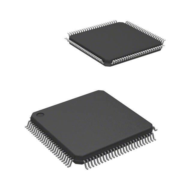


 工商网监
湘ICP备2023018690号
工商网监
湘ICP备2023018690号

