Product
Folder
Order
Now
Support &
Community
Tools &
Software
Technical
Documents
OPA363, OPA2363, OPA364, OPA2364, OPA4364
SBOS259F – SEPTEMBER 2002 – REVISED JUNE 2018
OPAx363, OPAx364 1.8-V, 7-MHz, 90-dB CMRR, Single-Supply, Rail-to-Rail I/O
Operational Amplifier
1 Features
•
•
•
•
•
•
•
•
1
1.8-V Operation
MicroSIZE Packages
Bandwidth: 7 MHz
CMRR: 90 dB (Typical)
Slew Rate: 5 V/µs
Low Offset: 500 µV (Maximum)
Quiescent Current: 750 µA/Channel (Maximum)
Shutdown Mode: Less Than 1 µA/Channel
2 Applications
•
•
•
•
•
Signal Conditioning
Data Acquisition
Process Control
Active Filters
Test Equipment
The single version is available in the MicroSize 5-pin
SOT-23 (6-pin SOT-23 for shutdown) and 8-pin
SOIC. The dual version is available in 8-pin VSSOP,
10-pin VSSOP, 16-pin UQFN, and 8-pin SOIC
packages. Quad packages are available in 14-pin
TSSOP and 14-pin SOIC packages. All versions are
specified for operation from –40°C to +125°C.
Device Information(1)
PART NUMBER
OPA363
OPA364
OPA2363
OPA2364
OPA4364
3 Description
The OPA363 and OPA364 families are highperformance, CMOS operational amplifiers optimized
for very low voltage, single-supply operation. These
miniature, low-cost amplifiers are designed to operate
on single supplies from 1.8 V (±0.9 V) to 5.5 V
(±2.75 V). Applications include sensor amplification
and signal conditioning in battery-powered systems.
PACKAGE
BODY SIZE (NOM)
SOT-23 (6)
2.60 mm × 1.60 mm
SOIC (8)
4.90 mm × 3.91 mm
SOT-23 (5)
2.60 mm × 1.60 mm
SOIC (8)
4.90 mm × 3.91 mm
VSSOP (10)
3.00 mm × 3.00 mm
UQFN (16)
2.60 mm × 1.80 mm
SOIC (8)
4.90 mm × 3.91 mm
VSSOP (8)
3.00 mm × 3.00 mm
SOIC (14)
8.65 mm × 3.91 mm
TSSOP (14)
5.00 mm × 4.40 mm
(1) For all available packages, see the orderable addendum at
the end of the data sheet.
Single-Supply Microphone Preamplifier
CFB
5V
130 pF
RFB
The OPA363 and OPA364 families offer excellent
CMRR without the crossover associated with
traditional complimentary input stages. This feature
results in excellent performance for driving analog-todigital (A/D) converters without degradation of
differential linearity and THD. The input commonmode range includes both the negative and positive
supplies. The output voltage swing is within 10 mV of
the rails.
The OPA363 family includes a shutdown mode.
Under logic control, the amplifiers can be switched
from normal operation to a standby current that is
less than 1 µA.
RBIAS
5.9 k
61.9 k
CIN
5V
0.1 F
1.5 F
Electret
Microphone
5V
RDIV
100 k
±
Output
+
RDIV
100 k
VS+
OPA364
VS±
CDIV
160 nF
Copyright © 2017, Texas Instruments Incorporated
1
An IMPORTANT NOTICE at the end of this data sheet addresses availability, warranty, changes, use in safety-critical applications,
intellectual property matters and other important disclaimers. PRODUCTION DATA.
�OPA363, OPA2363, OPA364, OPA2364, OPA4364
SBOS259F – SEPTEMBER 2002 – REVISED JUNE 2018
www.ti.com
Table of Contents
Features ..................................................................
Applications ...........................................................
Description .............................................................
Revision History.....................................................
Device Comparison Table.....................................
5.1 Device Comparison Table......................................... 4
9.1 Application Information............................................ 20
9.2 Typical Application .................................................. 23
6
7
Pin Configuration and Functions ......................... 4
Specifications......................................................... 8
10 Power Supply Recommendations ..................... 26
11 Layout................................................................... 26
7.1
7.2
7.3
7.4
7.5
7.6
7.7
7.8
7.9
7.10
8
1
1
1
2
4
8.2 Functional Block Diagram ....................................... 17
8.3 Feature Description................................................. 18
8.4 Device Functional Modes........................................ 19
1
2
3
4
5
Absolute Maximum Ratings ...................................... 8
ESD Ratings.............................................................. 8
Recommended Operating Conditions....................... 8
Thermal Information: OPA363 .................................. 9
Thermal Information: OPA364 .................................. 9
Thermal Information: OPA2363 .............................. 10
Thermal Information: OPA2364 .............................. 10
Thermal Information: OPA4364 .............................. 10
Electrical Characteristics......................................... 11
Typical Characteristics .......................................... 13
Detailed Description ............................................ 17
8.1 Overview ................................................................. 17
9
Application and Implementation ........................ 20
11.1 Layout Guidelines ................................................. 26
11.2 Layout Example .................................................... 26
12 Device and Documentation Support ................. 28
12.1
12.2
12.3
12.4
12.5
12.6
12.7
12.8
Device Support......................................................
Documentation Support ........................................
Related Links ........................................................
Receiving Notification of Documentation Updates
Community Resource............................................
Trademarks ...........................................................
Electrostatic Discharge Caution ............................
Glossary ................................................................
28
29
29
29
29
29
29
30
13 Mechanical, Packaging, and Orderable
Information ........................................................... 30
4 Revision History
NOTE: Page numbers for previous revisions may differ from page numbers in the current version.
Changes from Revision E (January 2018) to Revision F
Page
•
Changed OPA363 SOT-23 (5) to SOT-23 (6) in Device Information table ........................................................................... 1
•
Added OPA363 SOIC (8) package to Device Information table ............................................................................................ 1
•
Changed OPA364 SOT-23 (6) to SOT-23 (5) in Device Information table ........................................................................... 1
•
Deleted OPA2364 VSSOP (10) and UQFN (16) packages from Device Information table ................................................... 1
•
Deleted OPA2363 SOIC (8) and VSSOP (8) packages from Device Information table......................................................... 1
Changes from Revision D (September 2016) to Revision E
Page
•
Changed OPA36x and OPA236x part numbers to OPA364 and OPA2363 in Device Information table .............................. 1
•
Added OPA2364 device to Device Information table ............................................................................................................ 1
•
Corrected formatting of pinout drawings in Pin Configuration and Functions section............................................................ 4
•
Corrected formatting of pinout tables in Pin Configuration and Functions section ................................................................ 4
•
Added a minimum value of 0 V to supply voltage parameter in Absolute Maximum Ratings table ...................................... 8
•
Added "([V+] – [V–])" to supply voltage parameter in Absolute Maximum Ratings table ...................................................... 8
•
Deleted operating temperature range from Absolute Maximum Ratings table ...................................................................... 8
•
Added the word "temperature" to junction and storage temperature ranges in Absolute Maximum Ratings table ............... 8
•
Added "([V+] – [V–])" to supply voltage parameter in Recommended Operating Conditions table ...................................... 8
•
Changed output voltage swing parameter units from V to mV............................................................................................. 11
•
Deleted temperature range section of Electrical Characteristics table................................................................................. 11
•
Changed PSRR test condition from VCM = 0 to VCM = (V–) in Electrical Characteristics table ............................................ 11
•
Deleted Buffered Reference Voltage subsection in Application Information section .......................................................... 20
•
Changed Figure 33 .............................................................................................................................................................. 26
•
Added Figure 34 .................................................................................................................................................................. 27
2
Submit Documentation Feedback
Copyright © 2002–2018, Texas Instruments Incorporated
Product Folder Links: OPA363 OPA2363 OPA364 OPA2364 OPA4364
�OPA363, OPA2363, OPA364, OPA2364, OPA4364
www.ti.com
•
SBOS259F – SEPTEMBER 2002 – REVISED JUNE 2018
Changed "IC" to "device" throughout data sheet.................................................................................................................. 28
Changes from Revision C (May 2013) to Revision D
Page
•
Added ESD Ratings table, Feature Description section, Device Functional Modes, Application and Implementation
section, Power Supply Recommendations section, Layout section, Device and Documentation Support section, and
Mechanical, Packaging, and Orderable Information section ................................................................................................. 1
•
Deleted Package and Ordering Information section, see POA at the end of the datasheet.................................................. 1
Changes from Revision B (February 2003) to Revision C
Page
•
Converted data sheet to current format.................................................................................................................................. 1
•
Added RSV package (UQFN-16) to data sheet ..................................................................................................................... 1
•
Added text to last bullet of Layout Guidelines section.......................................................................................................... 26
Copyright © 2002–2018, Texas Instruments Incorporated
Submit Documentation Feedback
Product Folder Links: OPA363 OPA2363 OPA364 OPA2364 OPA4364
3
�OPA363, OPA2363, OPA364, OPA2364, OPA4364
SBOS259F – SEPTEMBER 2002 – REVISED JUNE 2018
www.ti.com
5 Device Comparison Table
5.1 Device Comparison Table
OPA363
OPA364
SOT-23-5
OPA2363
OPA2364
OPA4364
X
SOT-23-6 (shutdown)
X
MSOP-8
X
MSOP-10
X
SO-8
X
X
X
TSSOP-14
X
SO-14
X
UQFN-16
X
6 Pin Configuration and Functions
OPA363: DBV Package
6-Pin SOT-23
Top View
VOUT 1
2
A40
V
+IN 3
OPA363: D Package
8-Pin SOIC
Top View
6
V+
5
Enable
4
IN
NC 1
8
Enable
IN 2
7
V+
+IN 3
6
V
4
5
NC
V
(1)
OUT
Orient according to marking.
NC- no internal connection
Pin Functions: OPA363
PIN
I/O
DESCRIPTION
NAME
SOIC
SOT-23
Enable
8
5
I
Enable
–IN
2
4
I
Negative (inverting) input
+IN
3
3
I
Positive (noninverting) input
NC
1, 5
—
—
No internal connection (can be left floating)
VOUT
6
1
O
Output
V–
4
2
—
Negative (lowest) power supply
V+
7
6
—
Positive (highest) power supply
4
Submit Documentation Feedback
Copyright © 2002–2018, Texas Instruments Incorporated
Product Folder Links: OPA363 OPA2363 OPA364 OPA2364 OPA4364
�OPA363, OPA2363, OPA364, OPA2364, OPA4364
www.ti.com
SBOS259F – SEPTEMBER 2002 – REVISED JUNE 2018
V
OUT
B
8
IN B
4
7
+IN B
5
6
Enable B
+IN A
3
V
Enable A
B
+IN B
9
A
16
15
14
13
NC
1
12
NC
NC
2
11
Enable B
NC
3
10
Enable A
NC
4
9
NC
OUT A
5
6
7
8
V-
2
+V
-IN B
IN A
10
+IN A
1
OUT B
A
OUT
-IN A
V
OPA2363: RSV Package
16-Pin UQFN
Top View
V+
OPA2363: DGS Package
10-Pin MSOP
Top View
NC- no internal connection
Pin Functions: OPA2363
PIN
NAME
I/O
DESCRIPTION
MSOP
UQFN
Enable A
5
10
I
Enable A amplifier
Enable B
6
11
I
Enable B amplifier
–IN A
2
6
I
Inverting input, channel A
+IN A
3
7
I
Noninverting input, channel A
–IN B
8
14
I
Inverting input, channel B
+IN B
7
13
I
Noninverting input, channel B
NC
—
1, 2, 3,
4, 9, 12
—
No internal connection (can be left floating)
OUT A
—
5
O
Output, channel A
OUT B
—
15
O
Output, channel B
VOUT A
1
—
O
Output, channel A
VOUT B
9
—
O
Output, channel B
–V, V–
4
8
—
Negative (lowest) power supply
+V, V+
10
16
—
Positive (highest) power supply
Copyright © 2002–2018, Texas Instruments Incorporated
Submit Documentation Feedback
Product Folder Links: OPA363 OPA2363 OPA364 OPA2364 OPA4364
5
�OPA363, OPA2363, OPA364, OPA2364, OPA4364
SBOS259F – SEPTEMBER 2002 – REVISED JUNE 2018
www.ti.com
OPA364: DBV Package
5-Pin SOT-23
Top View
V
V
1
2
5
+IN 3
(1)
V+
A41
OUT
OPA364: D Package
8-Pin SOIC
Top View
4
IN
NC 1
8
NC
IN 2
7
V+
+IN 3
6
V
V
5
NC
4
OUT
Orient according to marking.
NC - no internal connection
Pin Functions: OPA364
PIN
NAME
I/O
DESCRIPTION
SOIC
SOT-23
–IN
2
4
I
Negative (inverting) input
+IN
3
3
I
Positive (noninverting) input
NC
1, 5, 8
—
—
No internal connection (can be left floating)
VOUT
6
1
O
Output
V–
4
2
—
Negative (lowest) power supply
V+
7
5
—
Positive (highest) power supply
OPA2364: DGK and D Packages
8-Pin MSOP and SOIC
Top View
OUT A 1
8
V+
IN A
2
7
OUT B
+IN A
3
6
IN B
V
4
5
+IN B
Pin Functions: OPA2364
PIN
I/O
DESCRIPTION
NAME
NO.
–IN A
2
I
Inverting input, channel A
+IN A
3
I
Noninverting input, channel A
–IN B
6
I
Inverting input, channel B
+IN B
5
I
Noninverting input, channel B
OUT A
1
O
Output, channel A
OUT B
7
O
Output, channel B
V–
4
—
Negative (lowest) power supply
V+
8
—
Positive (highest) power supply
6
Submit Documentation Feedback
Copyright © 2002–2018, Texas Instruments Incorporated
Product Folder Links: OPA363 OPA2363 OPA364 OPA2364 OPA4364
�OPA363, OPA2363, OPA364, OPA2364, OPA4364
www.ti.com
SBOS259F – SEPTEMBER 2002 – REVISED JUNE 2018
OPA4364: D and PW Packages
14-Pin SOIC and TSSOP
Top View
V
A
1
IN A
2
OUT
14
A
V
OUT
D
13
IN D
D
+IN A
3
12
+IN D
V+
4
11
V
+IN B
5
10
+IN C
IN C
B
V
C
IN B
6
9
B
7
8
OUT
V
OUT
C
NC- no internal connection.
Pin Functions: OPA4364
PIN
I/O
DESCRIPTION
NAME
NO.
–IN A
2
I
Inverting input, channel A
+IN A
3
I
Noninverting input, channel A
–IN B
6
I
Inverting input, channel B
+IN B
5
I
Noninverting input, channel B
–IN C
9
I
Inverting input, channel C
+IN C
10
I
Noninverting input, channel C
–IN D
13
I
Inverting input, channel D
+IN D
12
I
Noninverting input, channel D
VOUT A
1
O
Output, channel A
VOUT B
7
O
Output, channel B
VOUT C
8
O
Output, channel C
VOUT D
14
O
Output, channel D
V–
11
—
Negative (lowest) power supply
V+
4
—
Positive (highest) power supply
Copyright © 2002–2018, Texas Instruments Incorporated
Submit Documentation Feedback
Product Folder Links: OPA363 OPA2363 OPA364 OPA2364 OPA4364
7
�OPA363, OPA2363, OPA364, OPA2364, OPA4364
SBOS259F – SEPTEMBER 2002 – REVISED JUNE 2018
www.ti.com
7 Specifications
7.1 Absolute Maximum Ratings
over operating free-air temperature range (unless otherwise noted) (1)
MIN
MAX
0
5.5
Signal input pin (2)
−0.5
(V+) + 0.5
Signal input pin (2)
–10
Supply ([V+] – [V–])
Voltage
Current
Output short-circuit (3)
10
(3)
mA
mA
150
Storage temperature, Tstg
(2)
V
Continuous
Junction temperature, TJ
(1)
UNIT
–65
°C
150
Stresses beyond those listed under Absolute Maximum Ratings may cause permanent damage to the device. These are stress ratings
only, which do not imply functional operation of the device at these or any other conditions beyond those indicated under Recommended
Operating Conditions. Exposure to absolute-maximum-rated conditions for extended periods may affect device reliability.
Input terminals are diode-clamped to the power-supply rails. Input signals that can swing more than 0.5 V beyond the supply rails must
be current limited to 10 mA or less.
Short-circuit to ground, one amplifier per package.
7.2 ESD Ratings
VALUE
V(ESD)
(1)
(2)
Electrostatic discharge
Human-body model (HBM), per ANSI/ESDA/JEDEC JS-001
(1)
±2000
Charged-device model (CDM), per JEDEC specification JESD22-C101 (2)
±750
UNIT
V
JEDEC document JEP155 states that 500-V HBM allows safe manufacturing with a standard ESD control process.
JEDEC document JEP157 states that 250-V CDM allows safe manufacturing with a standard ESD control process.
7.3 Recommended Operating Conditions
over operating free-air temperature range (unless otherwise noted)
MIN
TA
8
NOM
MAX
UNIT
Supply voltage ([V+] – [V–])
1.8
5.5
V
Operating temperature
–40
125
°C
Submit Documentation Feedback
Copyright © 2002–2018, Texas Instruments Incorporated
Product Folder Links: OPA363 OPA2363 OPA364 OPA2364 OPA4364
�OPA363, OPA2363, OPA364, OPA2364, OPA4364
www.ti.com
SBOS259F – SEPTEMBER 2002 – REVISED JUNE 2018
7.4 Thermal Information: OPA363
OPA363
THERMAL METRIC (1)
DBV (SOT-23)
UNIT
5 PINS
RθJA
Junction-to-ambient thermal resistance
211.4
°C/W
RθJC(top)
RθJB
Junction-to-case (top) thermal resistance
137
°C/W
Junction-to-board thermal resistance
39.8
°C/W
ψJT
Junction-to-top characterization parameter
20.6
°C/W
ψJB
Junction-to-board characterization parameter
38.9
°C/W
RθJC(bot)
Junction-to-case (bottom) thermal resistance
—
°C/W
(1)
For more information about traditional and new thermal metrics, see the Semiconductor and IC Package Thermal Metrics application
report.
7.5 Thermal Information: OPA364
OPA364
THERMAL METRIC
(1)
DBV (SOT-23)
D (SOIC)
6 PINS
8 PINS
UNIT
RθJA
Junction-to-ambient thermal resistance
182.7
125.3
°C/W
RθJC(top)
Junction-to-case (top) thermal resistance
130.7
73.7
°C/W
RθJB
Junction-to-board thermal resistance
34.1
65.7
°C/W
ψJT
Junction-to-top characterization parameter
24.8
25.4
°C/W
ψJB
Junction-to-board characterization parameter
33.5
65.2
°C/W
RθJC(bot)
Junction-to-case (bottom) thermal resistance
—
—
°C/W
(1)
For more information about traditional and new thermal metrics, see the Semiconductor and IC Package Thermal Metrics application
report.
Copyright © 2002–2018, Texas Instruments Incorporated
Submit Documentation Feedback
Product Folder Links: OPA363 OPA2363 OPA364 OPA2364 OPA4364
9
�OPA363, OPA2363, OPA364, OPA2364, OPA4364
SBOS259F – SEPTEMBER 2002 – REVISED JUNE 2018
www.ti.com
7.6 Thermal Information: OPA2363
OPA2363
THERMAL METRIC (1)
D (SOIC)
DGK (VSSOP)
DGS (VSSOP)
UQFN (RSV)
8 PINS
8 PINS
10 PINS
16 PINS
UNIT
RθJA
Junction-to-ambient thermal resistance
125.3
171.8
166.4
112.4
°C/W
RθJC(to
Junction-to-case (top) thermal resistance
73.7
63.2
55.9
44
°C/W
RθJB
Junction-to-board thermal resistance
65.7
92.4
86.6
41.2
°C/W
ψJT
Junction-to-top characterization parameter
25.4
9.5
6.8
0.8
°C/W
ψJB
Junction-to-board characterization parameter
65.2
91
85.2
41.2
°C/W
RθJC(b
Junction-to-case (bottom) thermal resistance
—
—
—
—
°C/W
p)
ot)
(1)
For more information about traditional and new thermal metrics, see the Semiconductor and IC Package Thermal Metrics application
report.
7.7 Thermal Information: OPA2364
OPA2364
THERMAL METRIC (1)
D (SOIC)
DGK (VSSOP)
DGS (VSSOP)
UQFN (RSV)
8 PINS
8 PINS
10 PINS
16 PINS
UNIT
RθJA
Junction-to-ambient thermal resistance
125.3
171.8
166.4
112.4
°C/W
RθJC(to
Junction-to-case (top) thermal resistance
73.7
63.2
55.9
44
°C/W
RθJB
Junction-to-board thermal resistance
65.7
92.4
86.6
41.2
°C/W
ψJT
Junction-to-top characterization parameter
25.4
9.5
6.8
0.8
°C/W
ψJB
Junction-to-board characterization parameter
65.2
91
85.2
41.2
°C/W
RθJC(b
Junction-to-case (bottom) thermal resistance
—
—
—
—
°C/W
p)
ot)
(1)
For more information about traditional and new thermal metrics, see the Semiconductor and IC Package Thermal Metrics application
report.
7.8 Thermal Information: OPA4364
OPA4364
THERMAL METRIC
(1)
D (SOIC)
PW (TSSOP)
14 PINS
14 PINS
UNIT
RθJA
Junction-to-ambient thermal resistance
82.6
107.5
°C/W
RθJC(top)
Junction-to-case (top) thermal resistance
41.1
31.9
°C/W
RθJB
Junction-to-board thermal resistance
37.1
50.6
°C/W
ψJT
Junction-to-top characterization parameter
9.4
1.9
°C/W
ψJB
Junction-to-board characterization parameter
36.8
49.9
°C/W
RθJC(bot)
Junction-to-case (bottom) thermal resistance
—
—
°C/W
(1)
10
For more information about traditional and new thermal metrics, see the Semiconductor and IC Package Thermal Metrics application
report.
Submit Documentation Feedback
Copyright © 2002–2018, Texas Instruments Incorporated
Product Folder Links: OPA363 OPA2363 OPA364 OPA2364 OPA4364
�OPA363, OPA2363, OPA364, OPA2364, OPA4364
www.ti.com
SBOS259F – SEPTEMBER 2002 – REVISED JUNE 2018
7.9 Electrical Characteristics
at TA = 25°C, RL = 10 kΩ connected to VS / 2, VOUT = VS / 2, and VCM = VS / 2, VS = 1.8 V to 5.5 V, (unless otherwise noted)
PARAMETER
TEST CONDITIONS
MIN
TYP
MAX
UNIT
VS = 5 V (OPA363I, OPA364I)
500
µV
OPA2363I, OPA2364I
900
µV
2.5
mV
OFFSET VOLTAGE
VOS
Input offset voltage
dVOS/dT
PSRR
OPA363AI, OPA364AI, OPA2363AI, OPA2364AI, OPA4364AI
1
Drift
TA = –40°C to +125°C
3
Input offset voltage vs power
supply
VS = 1.8 V to 5.5 V
VCM = (V–)
TA = –40°C to +125°C
80
Channel separation, DC
µV/°C
330
1
µV/V
µV/V
INPUT BIAS CURRENT
IB
Input bias current
IOS
Input offset current
TA = 25°C
±1
TA = –40°C to +125°C
±10
pA
±10
pA
See Typical Characteristics
±1
NOISE
en
Input voltage noise,
f = 0.1 Hz to 10 Hz
10
µVPP
en
Input voltage noise density
f = 10 kHz
17
nV/√Hz
in
Input current noise density
f = 10 kHz
0.6
fA/√Hz
INPUT VOLTAGE RANGE
VCM
Common-mode voltage range
CMRR
Common-mode rejection ratio
(V–) – 0.1
(V−) – 0.1 V < VCM < (V+) + 0.1 V
TA = –40°C to +125°C
74
(V+) + 0.1
V
90
dB
Differential
2
pF
Common-mode
3
pF
100
dB
INPUT CAPACITANCE
OPEN-LOOP GAIN
AOL
Open-loop voltage gain
RL = 10 kΩ
100 mV < VO < (V+) – 100 mV
TA = 25°C
94
TA = 25°C (OPA4364)
90
dB
RL = 10 kΩ
100 mV < VO < (V+) – 100 mV
VS = 1.8 V to 5.5 V
TA = –40°C to +125°C
86
dB
FREQUENCY RESPONSE
GBW
Gain-bandwidth product
CL = 100 pF
7
MHz
SR
Slew rate
CL = 100 pF, G = 1
5
V/µs
0.1%, CL = 100 pF, VS = 5 V, 4-V step, G = 1
1
µs
0.01%, CL = 100 pF, VS = 5 V, 4-V step, G = 1
1.5
µs
Overload recovery time
CL = 100 pF
VIN × Gain > VS
0.8
µs
Total harmonic distortion + noise
CL = 100 pF, VS = 5 V, G = 1, f = 20 Hz to 20 kHz
tS
Settling time
THD+N
0.002%
OUTPUT
RL = 10 kΩ, TA = 25°C
Voltage output swing
10
RL = 10 kΩ
TA = –40°C to +125°C
ISC
Short-circuit current
See Typical Characteristics
CLOAD
Capacitive load drive
See Typical Characteristics
20
mV
20
mV
SHUTDOWN (OPA363)
tOFF
Turnoff time
tON
Turnon time (1)
VL
Logic low threshold
Shutdown
VH
Logic high threshold
Amplifier is active
IQ(sd)
Quiescent current at
shutdown (per amplifier)
(1)
1
µs
20
0.75 (V+)
µs
(V–) + 0.8
V
5.5
V
0.9
µA
Part is considered enabled when input offset voltage returns to specified range.
Copyright © 2002–2018, Texas Instruments Incorporated
Submit Documentation Feedback
Product Folder Links: OPA363 OPA2363 OPA364 OPA2364 OPA4364
11
�OPA363, OPA2363, OPA364, OPA2364, OPA4364
SBOS259F – SEPTEMBER 2002 – REVISED JUNE 2018
www.ti.com
Electrical Characteristics (continued)
at TA = 25°C, RL = 10 kΩ connected to VS / 2, VOUT = VS / 2, and VCM = VS / 2, VS = 1.8 V to 5.5 V, (unless otherwise noted)
PARAMETER
TEST CONDITIONS
MIN
TYP
MAX
UNIT
POWER SUPPLY
VS
IQ
12
Specified voltage range
1.8
Quiescent current (per amplifier)
Submit Documentation Feedback
5.5
V
650
750
µA
VS = 3.6 V
TA = –40°C to +125°C
850
1000
µA
VS = 5.5 V
TA = –40°C to +125°C
1.1
1.4
mA
VS = 1.8 V
TA = –40°C to +125°C
Copyright © 2002–2018, Texas Instruments Incorporated
Product Folder Links: OPA363 OPA2363 OPA364 OPA2364 OPA4364
�OPA363, OPA2363, OPA364, OPA2364, OPA4364
www.ti.com
SBOS259F – SEPTEMBER 2002 – REVISED JUNE 2018
7.10 Typical Characteristics
at TA = 25°C, RL = 10 kΩ connected to VS / 2, VOUT = VS / 2, and VCM = VS / 2, (unless otherwise noted)
-30
80
-60
60
-90
40
-120
20
-150
0
-180
90
80
70
CMRR (dB)
100
100
Phase (°)
0
Voltage Gain (dB)
120
60
50
40
30
20
10
-20
0
10
100
1k
10k
100k
1M
10M
100M
10
100
1k
Frequency (Hz)
10k
100k
1M
10M
Frequency (Hz)
Figure 1. Open-Loop Gain and Phase vs Frequency
Figure 2. Common-Mode Rejection Ratio vs Frequency
1.4
100
Per Amplifier
Quiescent Current (mA)
PSRR (dB)
80
60
40
20
1.2
1.0
0.8
0.6
0.4
0
1
10
100
1k
10k
100k
1M
1.5
10M
2.0
2.5
Figure 3. Power-Supply Rejection Ratio vs Frequency
VOUT = -10dBv
G = 10, RL = 2kW
VS = 1.8V
THD+N (%)
0.1
G = 1, RL = 2kW
VS = 1.8V
G = 1,
RL = 2kW
VS = 5V
0.0001
100
4.5
5.0
5.5
6.0
(VS = 5V, VOUT = 1Vrms)
0.1
0.001
10
4.0
Figure 4. Quiescent Current vs Supply Voltage
G = 10, RL = 2kW
VS = 5V
G = 10, RL = 10kW
VS = 1.8V, 5V
0.01
3.5
1
THD+N (%)
1
3.0
Supply Voltage (V)
Frequency (Hz)
1k
G = 1,
RL = 10kW
VS = 1.8V, 5V
0.01
G = 10, RL = 10kW
0.001
G = 1, RL = 2kW
G = 1, RL = 10kW
0.0001
10k
100k
Frequency (Hz)
Figure 5. Total Harmonic Distortion + Noise Ratio vs
Frequency
Copyright © 2002–2018, Texas Instruments Incorporated
G = 10, RL = 2kW
10
100
1k
10k
100k
Frequency (Hz)
Figure 6. Total Harmonic Distortion + Noise Ratio vs
Frequency
Submit Documentation Feedback
Product Folder Links: OPA363 OPA2363 OPA364 OPA2364 OPA4364
13
�OPA363, OPA2363, OPA364, OPA2364, OPA4364
SBOS259F – SEPTEMBER 2002 – REVISED JUNE 2018
www.ti.com
Typical Characteristics (continued)
at TA = 25°C, RL = 10 kΩ connected to VS / 2, VOUT = VS / 2, and VCM = VS / 2, (unless otherwise noted)
120
Short-Circuit Current (mA)
Input Voltage Noise (nV/ÖHz)
1000
100
10
100
+ISC
80
60
40
-ISC
20
0
10
100
1k
10k
100k
1.5
2.0
2.5
Frequency (Hz)
Figure 7. Input Voltage Noise Spectral Density vs Frequency
3
VS = ±1.65V
Input Bias Current (pA)
Output Voltage (V)
VS = ±0.9V
-1
TA = -40°C
TA = +25°C
TA = +125°C
-2
VS = ±1.65V
VS = ±2.5V
±10
±20
5.5
±30 ±40 ±50
±60
±70
0
-2
VCM = +5.1V
-4
-6
VCM = -0.1V
-10
-0.5
±80 ±90 ±100
0.5
1.5
2.5
3.5
4.5
5.5
Output Current (mA)
Common-Mode Voltage (V)
Figure 9. Output Voltage Swing vs Output Current
Figure 10. Input Bias Current vs Input Common-Mode
Voltage
10k
Input Bias Current (pA)
Input Offset Current (pA)
5.0
-8
10k
1k
100
10
1
-50
14
4.5
2
1
0
4.0
Figure 8. Short-Circuit Current vs Supply Voltage
2
-3
3.5
4
VS = ±2.5V
0
3.0
Supply Voltage (V)
-25
0
25
50
75
100
125
1k
100
10
1
-50
-25
0
25
50
75
100
125
Temperature (°C)
Temperature (°C)
Figure 11. Input Offset Current vs Temperature
Figure 12. Input Bias Current vs Temperature
Submit Documentation Feedback
Copyright © 2002–2018, Texas Instruments Incorporated
Product Folder Links: OPA363 OPA2363 OPA364 OPA2364 OPA4364
�OPA363, OPA2363, OPA364, OPA2364, OPA4364
www.ti.com
SBOS259F – SEPTEMBER 2002 – REVISED JUNE 2018
Typical Characteristics (continued)
at TA = 25°C, RL = 10 kΩ connected to VS / 2, VOUT = VS / 2, and VCM = VS / 2, (unless otherwise noted)
100
60
40
30
20
0.01%
Settling Time (ms)
Overshoot (%)
50
G = +1
10
0.1%
1
10
G = +10
0.1
0
100
1
1k
10
Figure 13. Small-Signal Overshoot vs Load Capacitance
Figure 14. Settling Time vs Closed-Loop Gain
20
16
Typical Production
Distribution of
Packaged Units
Percent of Amplifiers (%)
14
Percent of Amplifiers (%)
100
Closed-Loop Gain (V/V)
Load Capacitance (pF)
15
10
5
12
OPA36xAI
10
8
6
4
2
0
0
0
1
2
3
4
5
6
7
8
9
> 10
-2.5
-2.0
Offset Voltage Drift (mV/°C)
-1.0
0
1.0
2.0
2.5
Offset Voltage (mV)
Figure 15. Offset Drift Distribution
Figure 16. Offset Voltage Production Distribution
130
VENABLE
Channel Separation (dB)
VOUT
120
110
100
90
80
70
60
50
40
50ms/div
10
100
1k
10k
100k
1M
10M
Frequency (Hz)
Figure 17. Output Enable Characteristic (VS = 5 V,
VOUT = 20-kHz Sinusoid)
Copyright © 2002–2018, Texas Instruments Incorporated
Figure 18. Channel Separation vs Frequency
Submit Documentation Feedback
Product Folder Links: OPA363 OPA2363 OPA364 OPA2364 OPA4364
15
�OPA363, OPA2363, OPA364, OPA2364, OPA4364
SBOS259F – SEPTEMBER 2002 – REVISED JUNE 2018
www.ti.com
Typical Characteristics (continued)
1V/div
50mV/div
at TA = 25°C, RL = 10 kΩ connected to VS / 2, VOUT = VS / 2, and VCM = VS / 2, (unless otherwise noted)
250ns/div
CL = 100 pF
Figure 19. Small-Signal Step Response
16
Submit Documentation Feedback
1ms/div
CL = 100 pF
Figure 20. Large-Signal Step Response
Copyright © 2002–2018, Texas Instruments Incorporated
Product Folder Links: OPA363 OPA2363 OPA364 OPA2364 OPA4364
�OPA363, OPA2363, OPA364, OPA2364, OPA4364
www.ti.com
SBOS259F – SEPTEMBER 2002 – REVISED JUNE 2018
8 Detailed Description
8.1 Overview
The OPA363 and OPA364 series op amps are rail-to-rail operational amplifiers with excellent CMRR, low noise,
low offset, and wide bandwidth on supply voltages as low as ±0.9 V. The OPA363 features an additional pin for a
shutdown and enable function. These families do not exhibit phase reversal and are unity-gain stable. Specified
over the industrial temperature range of –40°C to +125°C, the OPA363 and OPA364 families offer precision
performance for a wide range of applications.
8.2 Functional Block Diagram
VS
Regulated
Charge Pump
VOUT = VCC +1.8 V
VCC + 1.8 V
IBIAS
Patent Pending
Very Low Ripple
Topology
IBIAS
VOUT
IBIAS
VIN-
VIN+
IBIAS
Copyright © 2017, Texas Instruments Incorporated
Copyright © 2002–2018, Texas Instruments Incorporated
Submit Documentation Feedback
Product Folder Links: OPA363 OPA2363 OPA364 OPA2364 OPA4364
17
�OPA363, OPA2363, OPA364, OPA2364, OPA4364
SBOS259F – SEPTEMBER 2002 – REVISED JUNE 2018
www.ti.com
8.3 Feature Description
8.3.1 Rail-to-Rail Input
The OPA363 and OPA364 feature excellent rail-to-rail operation, with supply voltages as low as ±0.9 V. The
input common-mode voltage range of the OPA363 and OPA364 family extends 100 mV beyond supply rails. The
unique input topology of the OPA363 and OPA364 eliminates the input offset transition region typical of most railto-rail, complementary stage operational amplifiers, allowing the OPA363 and OPA364 to provide superior
common-mode performance over the entire common-mode input range, as seen in Figure 21. This feature
prevents degradation of the differential linearity error and THD when driving A/D converters. A simplified
schematic of the OPA363 and OPA364 is shown in the Functional Block Diagram.
1.0
OPA363 and OPA364
0.5
0
VOS (mV)
-0.5
-1.0
-1.5
-2.0
Competitors
-2.5
-3.0
-3.5
-0.2
0
0.2
0.4
0.6
0.8
1.0 1.2
1.4
1.6
1.8
2.0
Common-Mode Voltage (V)
Figure 21. OPA363 and OPA364 Have Linear Offset Over Entire Common-Mode Range
8.3.2 Operating Voltage
The OPA363 and OPA364 series op amp parameters are fully specified from 1.8 V to 5.5 V. Single 0.1-µF
bypass capacitors must be placed across supply pins and as close to the part as possible. Supply voltages
higher than 5.5 V (absolute maximum) may cause permanent damage to the amplifier. Many specifications apply
from –40°C to +125°C. Parameters that vary significantly with operating voltages or temperature are shown in
the Typical Characteristics.
8.3.3 Capacitive Load
The OPAx363 and OPAx364 series op amps can drive a wide range of capacitive loads. However, all op amps
under certain conditions may become unstable. Op amp configuration, gain, and load value are a few of the
factors to consider when determining stability. An op amp in unity-gain configuration is the most susceptible to
the effects of capacitive load. The capacitive load reacts with the output resistance of the op amp to create a
pole in the small-signal response, which degrades the phase margin.
In unity gain, the OPAx363 and OPAx364 series op amps perform well with a pure capacitive load up to
approximately 1000 pF. The equivalent series resistance (ESR) of the loading capacitor may be sufficient to
allow the OPA363 and OPA364 to directly drive very large capacitive loads ( greater than 1 µF). Increasing gain
enhances the ability of the amplifier to drive more capacitance; see Figure 13.
One method of improving capacitive load drive in the unity-gain configuration is to insert a 10-Ω to 20-Ω resistor
in series with the output, as shown in Figure 22. This resistor significantly reduces ringing with large capacitive
loads. However, if there is a resistive load in parallel with the capacitive load, the load creates a voltage divider,
introduces a DC error at the output, and slightly reduces output swing. This error may be insignificant. For
example, with RL = 10 kΩ and RS = 20 Ω, there is an approximate 0.2% error at the output.
18
Submit Documentation Feedback
Copyright © 2002–2018, Texas Instruments Incorporated
Product Folder Links: OPA363 OPA2363 OPA364 OPA2364 OPA4364
�OPA363, OPA2363, OPA364, OPA2364, OPA4364
www.ti.com
SBOS259F – SEPTEMBER 2002 – REVISED JUNE 2018
Feature Description (continued)
V+
RS
OPAx363
OPAx364
VOUT
10 Ω to
20 Ω
VIN
RL
CL
Copyright © 2017, Texas Instruments Incorporated
Figure 22. Improving Capacitive Load Drive
8.3.4 Input and ESD Protection
All OPAx363 and OPAx364 pins are static-protected with internal ESD protection diodes tied to the supplies.
These diodes provide overdrive protection if the current is externally limited to 10 mA, as shown in the Absolute
Maximum Ratings and shown in Figure 23.
V+
IOVERLOAD
10-mA maximum
OPAx363
VOUT
VIN
5 kΩ
Copyright © 2017, Texas Instruments Incorporated
Figure 23. Input Current Protection
8.4 Device Functional Modes
8.4.1 Enable Function
The shutdown (enable) function of the OPAx363 is referenced to the negative supply voltage of the operational
amplifier. A logic level HIGH enables the op amp. A valid logic HIGH is defined as voltage greater than 75% of
the positive supply applied to the enable pin. The valid logic HIGH signal can be as much as 5.5 V above the
negative supply, independent of the positive supply voltage. A valid logic LOW is defined as less than 0.8 V
above the negative supply pin. If dual or split power supplies are used, take care to ensure that logic input
signals are properly referred to the negative supply voltage. This pin must be connected to a valid high or low
voltage or driven, not left open-circuit.
The logic input is a high-impedance CMOS input. Dual op amps are provided separate logic inputs. For batteryoperated applications, this feature reduces the average current and extend battery life. The enable time is 20 μs;
disable time is 1 μs. When disabled, the output assumes a high-impedance state. This configuration allows the
OPAx363 to operate as a gated amplifier, or to have the output multiplexed onto a common analog output bus.
Copyright © 2002–2018, Texas Instruments Incorporated
Submit Documentation Feedback
Product Folder Links: OPA363 OPA2363 OPA364 OPA2364 OPA4364
19
�OPA363, OPA2363, OPA364, OPA2364, OPA4364
SBOS259F – SEPTEMBER 2002 – REVISED JUNE 2018
www.ti.com
9 Application and Implementation
NOTE
Information in the following applications sections is not part of the TI component
specification, and TI does not warrant its accuracy or completeness. TI’s customers are
responsible for determining suitability of components for their purposes. Customers should
validate and test their design implementation to confirm system functionality.
9.1 Application Information
9.1.1 Achieving Output Swing to the Op Amp Negative Rail
Some applications require an accurate output voltage swing from 0 V to a positive full-scale voltage. A good
single-supply op amp may be able to swing within a few millivolts of single-supply ground, but as the output is
driven toward 0 V, the output stage of the amplifier prevents the output from reaching the negative supply rail of
the amplifier.
The output of the OPAx363 or OPAx364 can be made to swing to ground, or slightly below, on a single-supply
power source. To do so requires use of another resistor and an additional, more negative power supply than the
op amp negative supply. A pulldown resistor may be connected between the output and the additional negative
supply to pull the output down below the value that the output would otherwise achieve, as shown in Figure 24.
V+ = +5 V
OPA363
OPA364
VOUT
VIN
500 µA
Op Amp
Negative
Supply
Grounded
RP = 10 kΩ
-V = -5 V
(Additional
Negative Supply)
Copyright © 2017, Texas Instruments Incorporated
Figure 24. OPA363 and OPA364 Swing to Ground
This technique does not work with all op amps. The output stage of the OPAx363 and OPA3x64 allows the
output voltage to be pulled below that of most op amps, if approximately 500 µA is maintained through the output
stage. To calculate the appropriate value load resistor and negative supply, RL = –V / 500 µA. The OPAx363 and
OPAx364 are characterized to perform well under the described conditions, maintaining excellent accuracy down
to 0 V and as low as –10 mV. Limiting and nonlinearity occur below –10 mV, with linearity returning as the output
is again driven above –10 mV.
9.1.2 Directly Driving the ADS8324 and the MSP430
The OPAx363 and OPAx364 series op amps are optimized for driving medium speed (up to 100-kHz) sampling
A/D converters. However, they also offer excellent performance for higher speed converters. The no-crossover
input stage of the OPAx363 and OPAx364 directly drive A/D converters without degradation of differential
linearity and THD. They provide an effective means of buffering the A/D converter input capacitance and
resulting charge injection while providing signal gain. Figure 25 and Figure 26 show the OPAx363 and OPAx364
configured to drive the ADS8324 and the 12-bit A/D converter on the MSP430.
20
Submit Documentation Feedback
Copyright © 2002–2018, Texas Instruments Incorporated
Product Folder Links: OPA363 OPA2363 OPA364 OPA2364 OPA4364
�OPA363, OPA2363, OPA364, OPA2364, OPA4364
www.ti.com
SBOS259F – SEPTEMBER 2002 – REVISED JUNE 2018
Application Information (continued)
V+ = 1.8 V
V+ = 1.8 V
100 Ω
OPA363
OPA364
ADS8324
VIN
1 nF
Copyright © 2017, Texas Instruments Incorporated
Figure 25. OPAx363 and OPAx364 Directly Drive the ADS8324
V+
V+
100 Ω
OPA363
OPA364
MSP430
VIN
1 nF
Copyright © 2017, Texas Instruments Incorporated
Figure 26. Driving the 12-Bit A/D Converter on the MSP430
9.1.3 Audio Applications
The OPAx363 and OPAx364 op amp family has linear offset voltage over the entire input common-mode range.
Combined with low noise, this feature makes the OPAx363 and OPAx364 suitable for audio applications. Singlesupply, 1.8-V operation allows the OPA2363 and OPA2364 to be optimal candidates for dual stereo-headphone
drivers and microphone preamplifiers in portable stereo equipment; see Figure 27 and Figure 28.
20 kΩ
1 µF
V+
20 kΩ
One of Right or Left Channel
20 kΩ
1/2
OPA2363
20 kΩ
V+
10 kΩ
V-
1/2
TPS6100
47 pF
10 kΩ
One of Right or Left
Headphone Out
V-
Internally
Biased
V-
Copyright © 2017, Texas Instruments Incorporated
Figure 27. OPA2363 Configured as Half of a Dual Stereo-Headphone Driver
Copyright © 2002–2018, Texas Instruments Incorporated
Submit Documentation Feedback
Product Folder Links: OPA363 OPA2363 OPA364 OPA2364 OPA4364
21
�OPA363, OPA2363, OPA364, OPA2364, OPA4364
SBOS259F – SEPTEMBER 2002 – REVISED JUNE 2018
www.ti.com
Application Information (continued)
49 kΩ
Clean 3.3-V Supply
3.3 V
4 kΩ
OPAx363
OPAx364
Electret
Microphone
VOUT
5 kΩ
6 kΩ
1 µF
Copyright © 2017, Texas Instruments Incorporated
Figure 28. Microphone Preamplifier
9.1.4 Active Filtering
Low harmonic distortion and noise specifications plus high gain and slew rate make the OPAx363 and OPAx364
optimal candidates for active filtering. Figure 29 shows the OPA2363 configured as a low-distortion, third-order
general immittance converter (GIC) filter. Figure 30 shows the implementation of a Sallen-Key, 3-pole, low-pass
Bessel filter.
VIN
R1
R3
3.92 kΩ
1.33 kΩ
2
OPA363
R11
3.92 kΩ
6
7
1/2
OPA2363
2
VOUT
C4
1000 pF
3
R12
3.92 kΩ
6
3
1/2
OPA2363
1
C13
1000 pF
5
R14
3.48 kΩ
C15
1000 pF
Copyright © 2017, Texas Instruments Incorporated
Figure 29. OPA2363 as a Third-Order, 40-kHz, Low-Pass GIC Filter
220 pF
1.8 kΩ
19.5 kΩ
150 kΩ
VIN = 1 Vrms
3.3 nF
47 pF
OPA363
VOUT
Copyright © 2017, Texas Instruments Incorporated
Figure 30. OPAx363 or OPAx364 Configured as a 3-Pole, 20-kHz, Sallen-Key Filter
22
Submit Documentation Feedback
Copyright © 2002–2018, Texas Instruments Incorporated
Product Folder Links: OPA363 OPA2363 OPA364 OPA2364 OPA4364
�OPA363, OPA2363, OPA364, OPA2364, OPA4364
www.ti.com
SBOS259F – SEPTEMBER 2002 – REVISED JUNE 2018
9.2 Typical Application
9.2.1 Single-Supply Electret Microphone Preamplifier
Electret microphones are commonly used in portable electronics because of their small size, low cost, and
relatively good signal-to-noise ratio (SNR). The small package size and excellent AC performance of the
OPA364 make it an excellent choice for preamplifier circuits for electret microphones. The circuit shown in
Figure 31 is a single-supply preamplifier circuit for electret microphones.
CFB
5V
130 pF
RFB
RBIAS
5.9 k
61.9 k
CIN
5V
0.1 F
1.5 F
Electret
Microphone
5V
RDIV
100 k
±
Output
+
RDIV
100 k
VS+
OPA364
VS±
CDIV
160 nF
Copyright © 2017, Texas Instruments Incorporated
Figure 31. Preamplifier Circuit for Electret Microphones Using a Single-Supply Voltage
9.2.1.1 Design Requirements
•
•
•
•
•
•
5-V single supply
1-VRMS output for 100-dBSPL input
20-Hz to 20-kHz, –3-dB bandwidth
Microphone sensitivity: 8 µA/Pa
Microphone operating voltage: 2 V to 10 V
Microphone bias current: 500 µA
9.2.1.2 Detailed Design Procedure
In this circuit, the op amp is configured as a transimpedance amplifier which converts the signal current of the
microphone into an output voltage. The gain of the circuit is determined by the feedback resistor RFB, which must
be calculated according to the microphone sensitivity. For this design, a microphone output current of 8 µA per
Pascal (Pa) of air pressure was chosen. Using this value, the output current for a sound pressure level of 100
dBSPL, or 2 Pa air pressure, is calculated in Equation 1.
8 PA
imic
u 2 Pa = 16 PA
1 Pa
(1)
RFB is then calculated from this current to produce 1-VRMS output for a 100-dBSPL input signal in Equation 2.
VO 1 VRMS
RFB
62500 o 61.9 k:
imic 16 PA
(2)
The feedback capacitor (CFB) is calculated to limit the bandwidth of the amplifier to 20 kHz in Equation 3.
1
1
CFB
128.5 u 10 12 o 130 pF
2 ˜ S ˜ RFB ˜ fH 2 ˜ S ˜ (61.9 k:) ˜ (20 kHz)
(3)
Copyright © 2002–2018, Texas Instruments Incorporated
Submit Documentation Feedback
Product Folder Links: OPA363 OPA2363 OPA364 OPA2364 OPA4364
23
�OPA363, OPA2363, OPA364, OPA2364, OPA4364
SBOS259F – SEPTEMBER 2002 – REVISED JUNE 2018
www.ti.com
Typical Application (continued)
RBIAS is required to divert the microphone signal current through capacitor CIN rather than flowing from the power
supply, VCC. Larger values of RBIAS allow for a smaller capacitor to be used for CIN and reduce the overall noise
of the circuit. However, the maximum value for RBIAS is limited by the microphone bias current and minimum
operating voltage.
The value of RBIAS is calculated in Equation 4.
VCC VMIC 5 V 2 V
RBIAS
6000 o 5.9 k:
IBIAS
500 PA
(4)
Input capacitor CIN forms a high-pass filter in combination with resistor RBIAS. The filter corner frequency
calculation is shown in Equation 5 to place the high-pass corner frequency at 20 Hz.
1
1
CIN
1.349 u 10 6 o 1.5 PF
2 ˜ S ˜ RBIAS ˜ fL 2 ˜ S ˜ (5.9 k:) ˜ (20 Hz)
(5)
The voltage divider network at the op amp noninverting input is used to bias the op amp output to the mid-supply
point (VCC / 2) to maximize the output voltage range of the circuit. This result is easily achieved by selecting the
same value for both resistors in the divider. The absolute value of those resistors is limited by the acceptable
power-supply current drawn by the voltage divider. Selecting 25 µA as an acceptable limit of supply current gives
a value of 100 kΩ for the resistors in the divider, as Equation 6 shows.
VCC
5V
RDIV
100 k:
2 ˜ IDIV 2 ˜ 25 PA
(6)
Finally, to minimize the additional noise contribution from the voltage divider, a capacitor is placed at the op amp
noninverting input. This capacitor forms a low-pass filter with the parallel combination of the voltage divider
resistors. Selecting a filter corner frequency of 20 Hz minimizes the noise contribution of the voltage divider
inside the amplifier passband; see Equation 7.
1
1
CDIV
1.592 u 10 7 o 160 nF
§ RDIV ·
§ 100 k: ·
2˜S˜¨
¸ ˜ (20 Hz)
¸ ˜ fL 2 ˜ S ˜ ¨
2
©
¹
© 2 ¹
(7)
9.2.1.3 Application Curve
The transfer function of the microphone preamplifier circuit is shown in Figure 32. The nominal gain of the circuit
is 95.82 dB, or 61,800 V per amp of input current. The –3-dB bandwidth limits of the circuit are 17.99 Hz and
19.23 kHz.
24
Submit Documentation Feedback
Copyright © 2002–2018, Texas Instruments Incorporated
Product Folder Links: OPA363 OPA2363 OPA364 OPA2364 OPA4364
�OPA363, OPA2363, OPA364, OPA2364, OPA4364
www.ti.com
SBOS259F – SEPTEMBER 2002 – REVISED JUNE 2018
Typical Application (continued)
98
96
94
Gain (dB, V/A)
92
90
88
86
84
82
80
10
100
1k
10k
100k
Frequency (Hz)
C001
Figure 32. Microphone Preamplifier Transfer Function
Copyright © 2002–2018, Texas Instruments Incorporated
Submit Documentation Feedback
Product Folder Links: OPA363 OPA2363 OPA364 OPA2364 OPA4364
25
�OPA363, OPA2363, OPA364, OPA2364, OPA4364
SBOS259F – SEPTEMBER 2002 – REVISED JUNE 2018
www.ti.com
10 Power Supply Recommendations
The OPAx363 and OPAx364 are specified for operation from 2.7 V to 5.5 V (±1.35 V to ±2.75 V). Parameters
that can exhibit significant variance with regard to operating voltage are presented in the Electrical
Characteristics.
11 Layout
11.1 Layout Guidelines
For best operational performance of the device, use good printed-circuit board (PCB) layout practices, including:
• Noise can propagate into analog circuitry through the power pins of the circuit as a whole and of op amp
itself. Bypass capacitors reduce the coupled noise by providing low-impedance power sources local to the
analog circuitry.
– Connect low-ESR, 0.1-µF ceramic bypass capacitors between each supply pin and ground, placed as
close to the device as possible. A single bypass capacitor from V+ to ground is applicable for singlesupply applications.
• Separate grounding for analog and digital portions of circuitry is one of the simplest and most effective
methods of noise suppression. One or more layers on multilayer PCBs are usually devoted to ground planes.
A ground plane helps distribute heat and reduces EMI noise pickup. Make sure to physically separate digital
and analog grounds, paying attention to the flow of the ground current.
• To reduce parasitic coupling, run the input traces as far away from the supply or output traces as possible. If
these traces cannot be kept separate, crossing the sensitive trace perpendicular is much better as opposed to
in parallel with the noisy trace.
• Place the external components as close to the device as possible. As shown in Figure 33, keeping RF and RG
close to the inverting input minimizes parasitic capacitance.
• Keep the length of input traces as short as possible. Always remember that the input traces are the most
sensitive part of the circuit.
• Consider a driven, low-impedance guard ring around the critical traces. A guard ring can significantly reduce
leakage currents from nearby traces that are at different potentials.
• Cleaning the PCB following board assembly is recommended for best performance.
• Any precision integrated circuit can experience performance shifts resulting from moisture ingress into the
plastic package. Following any aqueous PCB cleaning process, baking the PCB assembly is recommended to
remove moisture introduced into the device packaging during the cleaning process. A low temperature, postcleaning bake at 85°C for 30 minutes is sufficient for most circumstances.
11.2 Layout Example
GND
V+
GND
INPUT
OUTPUT
GND
VGND
Figure 33. Operational Amplifier Board Layout for Noninverting Configuration
26
Submit Documentation Feedback
Copyright © 2002–2018, Texas Instruments Incorporated
Product Folder Links: OPA363 OPA2363 OPA364 OPA2364 OPA4364
�OPA363, OPA2363, OPA364, OPA2364, OPA4364
www.ti.com
SBOS259F – SEPTEMBER 2002 – REVISED JUNE 2018
Layout Example (continued)
VC3
INPUT
4
GND
OUTPUT
U1
3
R3
6
7
2
C4
C2
V+
GND
GND
R1
C1
R2
GND
Figure 34. Layout Example Schematic
Copyright © 2002–2018, Texas Instruments Incorporated
Submit Documentation Feedback
Product Folder Links: OPA363 OPA2363 OPA364 OPA2364 OPA4364
27
�OPA363, OPA2363, OPA364, OPA2364, OPA4364
SBOS259F – SEPTEMBER 2002 – REVISED JUNE 2018
www.ti.com
12 Device and Documentation Support
12.1 Device Support
12.1.1 Development Support
12.1.1.1 TINA-TI™ (Free Software Download)
TINA™ is a simple, powerful, and easy-to-use circuit simulation program based on a SPICE engine. TINA-TI™ is
a free, fully-functional version of the TINA software, preloaded with a library of macro models in addition to a
range of both passive and active models. TINA-TI provides all the conventional dc, transient, and frequency
domain analysis of SPICE, as well as additional design capabilities.
Available as a free download from the Analog eLab Design Center, TINA-TI offers extensive post-processing
capability that allows users to format results in a variety of ways. Virtual instruments offer the ability to select
input waveforms and probe circuit nodes, voltages, and waveforms, creating a dynamic quick-start tool.
NOTE
These files require that either the TINA software (from DesignSoft™) or TINA-TI software
be installed. Download the free TINA-TI software from the TINA-TI folder.
12.1.1.2 DIP Adapter EVM
The DIP Adapter EVM tool provides an easy, low-cost way to prototype small surface mount devices. The
evaluation tool these TI packages: D or U (8-pin SOIC), PW (8-pin TSSOP), DGK (8-pin MSOP), DBV (6-pin
SOT-23, 5-pin SOT-23, and 3-pin SOT-23), DCK (6-pin SC-70 and 5-pin SC-70), and DRL (6-pin SOT-563). The
DIP Adapter EVM may also be used with terminal strips or may be wired directly to existing circuits.
12.1.1.3 Universal Op Amp EVM
The Universal Op Amp EVM is a series of general-purpose, blank circuit boards that simplify prototyping circuits
for a variety of device package types. The evaluation module board design allows many different circuits to be
constructed easily and quickly. Five models are offered, with each model intended for a specific package type.
PDIP, SOIC, MSOP, TSSOP and SOT-23 packages are all supported.
NOTE
These boards are unpopulated, so users must provide their own devices. TI recommends
requesting several op amp device samples when ordering the Universal Op Amp EVM.
12.1.1.4 TI Precision Designs
TI Precision Designs are analog solutions created by TI’s precision analog applications experts and offer the
theory of operation, component selection, simulation, complete PCB schematic and layout, bill of materials, and
measured performance of many useful circuits. TI Precision Designs are available online at
http://www.ti.com/ww/en/analog/precision-designs/.
12.1.1.5 WEBENCH® Filter Designer
WEBENCH® Filter Designer is a simple, powerful, and easy-to-use active filter design program. The WEBENCH
Filter Designer allows the user to create optimized filter designs using a selection of TI operational amplifiers and
passive components from TI's vendor partners.
Available as a web-based tool from the WEBENCH® Design Center, WEBENCH® Filter Designer allows the
user to design, optimize, and simulate complete multistage active filter solutions within minutes.
28
Submit Documentation Feedback
Copyright © 2002–2018, Texas Instruments Incorporated
Product Folder Links: OPA363 OPA2363 OPA364 OPA2364 OPA4364
�OPA363, OPA2363, OPA364, OPA2364, OPA4364
www.ti.com
SBOS259F – SEPTEMBER 2002 – REVISED JUNE 2018
12.2 Documentation Support
12.2.1 Related Documentation
The following documents are relevant to using the OPAx363 and OPAx364, and are recommended for reference.
All are available for download at www.ti.com (unless otherwise noted):
• AB-045 Op Amp Performance Analysis
• AB-067 Single-Supply Operation of Operational Amplifiers
• AB-105 Tuning in Amplifiers
• QFN/SON PCB Attachment
• Quad Flatpack No-Lead Logic Packages
12.3 Related Links
The table below lists quick access links. Categories include technical documents, support and community
resources, tools and software, and quick access to sample or buy.
Table 1. Related Links
PARTS
PRODUCT FOLDER
ORDER NOW
TECHNICAL
DOCUMENTS
TOOLS &
SOFTWARE
SUPPORT &
COMMUNITY
OPA363
Click here
Click here
Click here
Click here
Click here
OPA2363
Click here
Click here
Click here
Click here
Click here
OPA364
Click here
Click here
Click here
Click here
Click here
OPA2364
Click here
Click here
Click here
Click here
Click here
OPA4364
Click here
Click here
Click here
Click here
Click here
12.4 Receiving Notification of Documentation Updates
To receive notification of documentation updates, navigate to the device product folder on ti.com. In the upper
right corner, click on Alert me to register and receive a weekly digest of any product information that has
changed. For change details, review the revision history included in any revised document.
12.5 Community Resource
The following links connect to TI community resources. Linked contents are provided "AS IS" by the respective
contributors. They do not constitute TI specifications and do not necessarily reflect TI's views; see TI's Terms of
Use.
TI E2E™ Online Community TI's Engineer-to-Engineer (E2E) Community. Created to foster collaboration
among engineers. At e2e.ti.com, you can ask questions, share knowledge, explore ideas and help
solve problems with fellow engineers.
Design Support TI's Design Support Quickly find helpful E2E forums along with design support tools and
contact information for technical support.
12.6 Trademarks
TINA-TI, E2E are trademarks of Texas Instruments.
WEBENCH is a registered trademark of Texas Instruments.
TINA, DesignSoft are trademarks of DesignSoft, Inc.
All other trademarks are the property of their respective owners.
12.7 Electrostatic Discharge Caution
These devices have limited built-in ESD protection. The leads should be shorted together or the device placed in conductive foam
during storage or handling to prevent electrostatic damage to the MOS gates.
Copyright © 2002–2018, Texas Instruments Incorporated
Submit Documentation Feedback
Product Folder Links: OPA363 OPA2363 OPA364 OPA2364 OPA4364
29
�OPA363, OPA2363, OPA364, OPA2364, OPA4364
SBOS259F – SEPTEMBER 2002 – REVISED JUNE 2018
www.ti.com
12.8 Glossary
SLYZ022 — TI Glossary.
This glossary lists and explains terms, acronyms, and definitions.
13 Mechanical, Packaging, and Orderable Information
The following pages include mechanical, packaging, and orderable information. This information is the most
current data available for the designated devices. This data is subject to change without notice and revision of
this document. For browser-based versions of this data sheet, refer to the left-hand navigation.
30
Submit Documentation Feedback
Copyright © 2002–2018, Texas Instruments Incorporated
Product Folder Links: OPA363 OPA2363 OPA364 OPA2364 OPA4364
�PACKAGE OPTION ADDENDUM
www.ti.com
14-Oct-2022
PACKAGING INFORMATION
Orderable Device
Status
(1)
Package Type Package Pins Package
Drawing
Qty
Eco Plan
(2)
Lead finish/
Ball material
MSL Peak Temp
Op Temp (°C)
Device Marking
(3)
Samples
(4/5)
(6)
OPA2363AIDGSR
ACTIVE
VSSOP
DGS
10
2500
RoHS & Green
Call TI
Level-2-260C-1 YEAR
-40 to 125
BHK
Samples
OPA2363AIDGST
ACTIVE
VSSOP
DGS
10
250
RoHS & Green
Call TI
Level-2-260C-1 YEAR
-40 to 125
BHK
Samples
OPA2363AIRSVR
ACTIVE
UQFN
RSV
16
3000
RoHS & Green
NIPDAUAG
Level-2-260C-1 YEAR
-40 to 125
SIN
Samples
OPA2363IDGSR
ACTIVE
VSSOP
DGS
10
2500
RoHS & Green
Call TI
Level-2-260C-1 YEAR
-40 to 125
BHK
Samples
OPA2363IDGST
ACTIVE
VSSOP
DGS
10
250
RoHS & Green
Call TI
Level-2-260C-1 YEAR
-40 to 125
BHK
Samples
OPA2364AID
ACTIVE
SOIC
D
8
75
RoHS & Green
Call TI
Level-2-260C-1 YEAR
-40 to 125
OPA
2364
A
OPA2364AIDG4
ACTIVE
SOIC
D
8
75
RoHS & Green
Call TI
Level-2-260C-1 YEAR
-40 to 125
OPA
2364
A
OPA2364AIDGKR
ACTIVE
VSSOP
DGK
8
2500
RoHS & Green
Call TI
Level-2-260C-1 YEAR
-40 to 125
BHL
Samples
OPA2364AIDGKT
ACTIVE
VSSOP
DGK
8
250
RoHS & Green
Call TI
Level-2-260C-1 YEAR
-40 to 125
BHL
Samples
OPA2364AIDR
ACTIVE
SOIC
D
8
2500
RoHS & Green
Call TI
Level-2-260C-1 YEAR
-40 to 125
OPA
2364
A
OPA2364AIDRG4
ACTIVE
SOIC
D
8
2500
RoHS & Green
Call TI
Level-2-260C-1 YEAR
-40 to 125
OPA
2364
A
OPA2364ID
ACTIVE
SOIC
D
8
75
RoHS & Green
Call TI
Level-2-260C-1 YEAR
-40 to 125
OPA
2364
Samples
OPA2364IDGKR
ACTIVE
VSSOP
DGK
8
2500
RoHS & Green
Call TI
Level-2-260C-1 YEAR
-40 to 125
BHL
Samples
OPA2364IDGKT
ACTIVE
VSSOP
DGK
8
250
RoHS & Green
Call TI
Level-2-260C-1 YEAR
-40 to 125
BHL
Samples
OPA2364IDGKTG4
ACTIVE
VSSOP
DGK
8
250
RoHS & Green
Call TI
Level-2-260C-1 YEAR
-40 to 125
BHL
Samples
OPA2364IDR
ACTIVE
SOIC
D
8
2500
RoHS & Green
Call TI
Level-2-260C-1 YEAR
-40 to 125
OPA
2364
Samples
OPA363AID
ACTIVE
SOIC
D
8
75
RoHS & Green
Call TI
Level-2-260C-1 YEAR
-40 to 125
OPA
Samples
Addendum-Page 1
Samples
Samples
Samples
Samples
�PACKAGE OPTION ADDENDUM
www.ti.com
14-Oct-2022
Orderable Device
Status
(1)
Package Type Package Pins Package
Drawing
Qty
Eco Plan
(2)
Lead finish/
Ball material
MSL Peak Temp
Op Temp (°C)
Device Marking
(3)
Samples
(4/5)
(6)
363
A
OPA363AIDBVR
ACTIVE
SOT-23
DBV
6
3000
RoHS & Green
NIPDAU
Level-2-260C-1 YEAR
-40 to 125
A40
Samples
OPA363AIDBVT
ACTIVE
SOT-23
DBV
6
250
RoHS & Green
NIPDAU
Level-2-260C-1 YEAR
-40 to 125
A40
Samples
OPA363AIDBVTG4
ACTIVE
SOT-23
DBV
6
250
RoHS & Green
NIPDAU
Level-2-260C-1 YEAR
-40 to 125
A40
Samples
OPA363ID
ACTIVE
SOIC
D
8
75
RoHS & Green
Call TI
Level-2-260C-1 YEAR
-40 to 125
OPA
363
Samples
OPA363IDBVR
ACTIVE
SOT-23
DBV
6
3000
RoHS & Green
NIPDAU
Level-2-260C-1 YEAR
-40 to 125
A40
Samples
OPA363IDBVT
ACTIVE
SOT-23
DBV
6
250
RoHS & Green
NIPDAU
Level-2-260C-1 YEAR
-40 to 125
A40
Samples
OPA364AID
ACTIVE
SOIC
D
8
75
RoHS & Green
Call TI
Level-2-260C-1 YEAR
-40 to 125
OPA
364
A
OPA364AIDBVR
ACTIVE
SOT-23
DBV
5
3000
RoHS & Green
NIPDAU
Level-2-260C-1 YEAR
-40 to 125
A41
Samples
OPA364AIDBVT
ACTIVE
SOT-23
DBV
5
250
RoHS & Green
NIPDAU
Level-2-260C-1 YEAR
-40 to 125
A41
Samples
OPA364AIDBVTG4
ACTIVE
SOT-23
DBV
5
250
RoHS & Green
NIPDAU
Level-2-260C-1 YEAR
-40 to 125
A41
Samples
OPA364AIDR
ACTIVE
SOIC
D
8
2500
RoHS & Green
Call TI
Level-2-260C-1 YEAR
-40 to 125
OPA
364
A
OPA364ID
ACTIVE
SOIC
D
8
75
RoHS & Green
Call TI
Level-2-260C-1 YEAR
-40 to 125
OPA
364
Samples
OPA364IDBVR
ACTIVE
SOT-23
DBV
5
3000
RoHS & Green
NIPDAU
Level-2-260C-1 YEAR
-40 to 125
A41
Samples
OPA364IDBVT
ACTIVE
SOT-23
DBV
5
250
RoHS & Green
NIPDAU
Level-2-260C-1 YEAR
-40 to 125
A41
Samples
OPA364IDBVTG4
ACTIVE
SOT-23
DBV
5
250
RoHS & Green
NIPDAU
Level-2-260C-1 YEAR
-40 to 125
A41
Samples
OPA364IDG4
ACTIVE
SOIC
D
8
75
RoHS & Green
Call TI
Level-2-260C-1 YEAR
-40 to 125
OPA
364
Samples
OPA364IDR
ACTIVE
SOIC
D
8
2500
RoHS & Green
Call TI
Level-2-260C-1 YEAR
-40 to 125
OPA
364
Samples
OPA4364AID
ACTIVE
SOIC
D
14
50
RoHS & Green
NIPDAU
Level-2-260C-1 YEAR
-40 to 125
OPA4364A
Samples
Addendum-Page 2
Samples
Samples
�PACKAGE OPTION ADDENDUM
www.ti.com
Orderable Device
14-Oct-2022
Status
(1)
Package Type Package Pins Package
Drawing
Qty
Eco Plan
(2)
Lead finish/
Ball material
MSL Peak Temp
Op Temp (°C)
Device Marking
(3)
Samples
(4/5)
(6)
OPA4364AIDR
ACTIVE
SOIC
D
14
2500
RoHS & Green
NIPDAU
Level-2-260C-1 YEAR
-40 to 125
OPA4364A
Samples
OPA4364AIDRG4
ACTIVE
SOIC
D
14
2500
RoHS & Green
NIPDAU
Level-2-260C-1 YEAR
-40 to 125
OPA4364A
Samples
OPA4364AIPWR
ACTIVE
TSSOP
PW
14
2500
RoHS & Green
NIPDAU
Level-2-260C-1 YEAR
-40 to 125
OPA
4364A
Samples
OPA4364AIPWT
ACTIVE
TSSOP
PW
14
250
RoHS & Green
NIPDAU
Level-2-260C-1 YEAR
-40 to 125
OPA
4364A
Samples
OPA4364AIPWTG4
ACTIVE
TSSOP
PW
14
250
RoHS & Green
NIPDAU
Level-2-260C-1 YEAR
-40 to 125
OPA
4364A
Samples
(1)
The marketing status values are defined as follows:
ACTIVE: Product device recommended for new designs.
LIFEBUY: TI has announced that the device will be discontinued, and a lifetime-buy period is in effect.
NRND: Not recommended for new designs. Device is in production to support existing customers, but TI does not recommend using this part in a new design.
PREVIEW: Device has been announced but is not in production. Samples may or may not be available.
OBSOLETE: TI has discontinued the production of the device.
(2)
RoHS: TI defines "RoHS" to mean semiconductor products that are compliant with the current EU RoHS requirements for all 10 RoHS substances, including the requirement that RoHS substance
do not exceed 0.1% by weight in homogeneous materials. Where designed to be soldered at high temperatures, "RoHS" products are suitable for use in specified lead-free processes. TI may
reference these types of products as "Pb-Free".
RoHS Exempt: TI defines "RoHS Exempt" to mean products that contain lead but are compliant with EU RoHS pursuant to a specific EU RoHS exemption.
Green: TI defines "Green" to mean the content of Chlorine (Cl) and Bromine (Br) based flame retardants meet JS709B low halogen requirements of
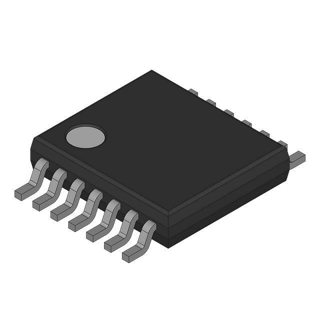


 工商网监
湘ICP备2023018690号
工商网监
湘ICP备2023018690号
