Product
Folder
Sample &
Buy
Support &
Community
Tools &
Software
Technical
Documents
OPA541
SBOS153B – SEPTEMBER 2000 – REVISED JANUARY 2016
OPA541 High Power Monolithic Operational Amplifier
1 Features
3 Description
•
•
•
•
•
•
The OPA541 device is a power-operational amplifier
capable of operation from power supplies up to
±40 V, and delivering continuous output currents up
to 5 A. Internal current-limit circuitry can be userprogrammed with a single external resistor, protecting
the amplifier and load from fault conditions. The
OPA541 devices fabricated are using a proprietary
bipolar and FET process.
1
Power Supplies to ±40 V
Output Current to 10-A Peak
Programmable Current Limit
Industry-Standard Pinout
FET Input
TO-3 and Low-Cost Power Plastic Packages
The OPA541 uses a single current-limit resistor to set
both the positive and negative current limits.
Applications currently using hybrid power amplifiers
requiring two current-limit resistors do need not to be
modified.
2 Applications
•
•
•
•
•
Motor Drivers
Servo Amplifiers
Synchro Excitation
Audio Amplifiers
Programmable Power Supplies
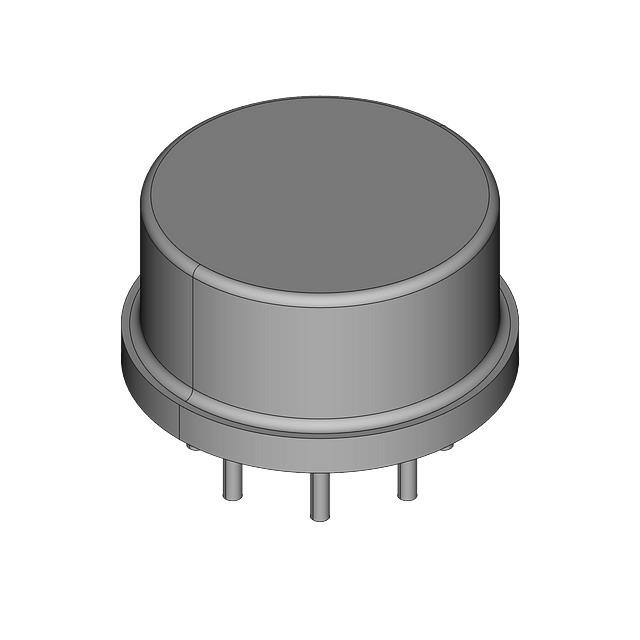
The OPA541 is available in an 11-pin power plastic
package and an industry-standard 8-pin TO-3
hermetic package. The power plastic pachage has a
copper-lead frame to maximize heat transfer. The
TO-3 package is isolated from all circuitry, allowing it
to be mounted directly to a heat sink without special
insulators.
Device Information(1)
PART NUMBER
OPA541
PACKAGE
TO-220 (11)
BODY SIZE (NOM)
10.70 mm × 20.02 mm
(1) For all available packages, see the orderable addendum at
the end of the data sheet.
Simplified Schematic
+VS
–In
+In
Current
Sense
R CL
Output
Drive
VO
External
–VS
1
An IMPORTANT NOTICE at the end of this data sheet addresses availability, warranty, changes, use in safety-critical applications,
intellectual property matters and other important disclaimers. PRODUCTION DATA.
�OPA541
SBOS153B – SEPTEMBER 2000 – REVISED JANUARY 2016
www.ti.com
Table of Contents
1
2
3
4
5
6
7
Features ..................................................................
Applications ...........................................................
Description .............................................................
Revision History.....................................................
Pin Configuration and Functions .........................
Specifications.........................................................
1
1
1
2
3
4
6.1
6.2
6.3
6.4
6.5
6.6
4
4
4
4
5
6
Absolute Maximum Ratings ......................................
ESD Ratings ............................................................
Recommended Operating Conditions.......................
Thermal Information ..................................................
Electrical Characteristics...........................................
Typical Characteristics ..............................................
Detailed Description .............................................. 8
7.1 Overview ................................................................... 8
7.2 Functional Block Diagram ......................................... 8
7.3 Feature Description................................................... 8
7.4 Device Functional Modes.......................................... 8
8
Application and Implementation .......................... 9
8.1 Application Information.............................................. 9
8.2 Typical Applications ............................................... 11
9 Power Supply Recommendations...................... 15
10 Layout................................................................... 15
10.1 Layout Guidelines ................................................. 15
10.2 Layout Example .................................................... 15
11 Device and Documentation Support ................. 16
11.1
11.2
11.3
11.4
11.5
Documentation Support .......................................
Community Resources..........................................
Trademarks ...........................................................
Electrostatic Discharge Caution ............................
Glossary ................................................................
16
16
16
16
16
12 Mechanical, Packaging, and Orderable
Information ........................................................... 16
4 Revision History
NOTE: Page numbers for previous revisions may differ from page numbers in the current version.
Changes from Revision A (August 2006) to Revision B
Page
•
Added ESD Ratings table, Thermal Information tables, Feature Description section, Device Functional Modes,
Application and Implementation section, Power Supply Recommendations section, Layout section, Device and
Documentation Support section, and Mechanical, Packaging, and Orderable Information section ..................................... 1
•
Deleted THERMAL RESISTANCE section from Electrical Characteristics............................................................................ 5
2
Submit Documentation Feedback
Copyright © 2000–2016, Texas Instruments Incorporated
Product Folder Links: OPA541
�OPA541
www.ti.com
SBOS153B – SEPTEMBER 2000 – REVISED JANUARY 2016
5 Pin Configuration and Functions
KV Package
11-Pin TO-220
Top View
Tab at −VS. Do not use to conduct current.
2
4
6
−In
1
3
5
+In
NC
7
9
11
NC
Output
Drive
−VS
10
8
Current
Sense
RCL
+VS
VO
Pin Functions
PIN
NO.
1
NAME
+In
I/O
DESCRIPTION
I
+Input
2
–In
I
-Input
3
–Vs
–
Negative power supply
4
–Vs
–
Negative power supply
5
Output
O
Output
6
NC
–
No internal connection
7
Output
O
Output
8
Current Sense
I
Current sensing input pin
9
NC
–
No internal connection
10
+Vs
–
Positive power supply
11
+Vs
–
Positive power supply
Submit Documentation Feedback
Copyright © 2000–2016, Texas Instruments Incorporated
Product Folder Links: OPA541
3
�OPA541
SBOS153B – SEPTEMBER 2000 – REVISED JANUARY 2016
www.ti.com
6 Specifications
6.1 Absolute Maximum Ratings
over operating free-air temperature range (unless otherwise noted)
(1)
MIN
MAX
UNIT
80
V
Supply voltage, +VS to –VS
Output current
See SOA, Figure 11
Power dissipation, Internal (2)
125
Input voltage, differential
+VS
Input voltage, common-mode
+VS
Temperature, pin solder, 10 s
300
°C
Junction temperature (2)
150
°C
Operating temperature (case)
Storage temperature, Tstg
(1)
(2)
AP
–40
85
AM, BM, SM
–55
125
AP
–25
85
AM, BM, SM
–65
150
W
°C
°C
Stresses beyond those listed under Absolute Maximum Ratings may cause permanent damage to the device. These are stress ratings
only, which do not imply functional operation of the device at these or any other conditions beyond those indicated under Recommended
Operating Conditions. Exposure to absolute-maximum-rated conditions for extended periods may affect device reliability.
Long term operation at the maximum junction temperature will result in reduced product life. Derate internal power dissipation to achieve
high MTTF.
6.2 ESD Ratings
VALUE
V(ESD)
(1)
(2)
Electrostatic discharge
Human-body model (HBM), per ANSI/ESDA/JEDEC JS-001 (1)
±2000
Charged-device model (CDM), per JEDEC specification JESD22-C101 (2)
±250
UNIT
V
JEDEC document JEP155 states that 500-V HBM allows safe manufacturing with a standard ESD control process.
JEDEC document JEP157 states that 250-V CDM allows safe manufacturing with a standard ESD control process.
6.3 Recommended Operating Conditions
over operating free-air temperature range (unless otherwise noted)
Supply Voltage (V+ – V–)
MIN
MAX
10 (±5)
80 (±40)
V
–40
125
°C
Specified temperature
UNIT
6.4 Thermal Information
OPA541
THERMAL METRIC (1)
KV (TO-220)
LMF (TO-3)
11 PINS
8 PINS
UNIT
RθJA
Junction-to-ambient thermal resistance
21.5
—
°C/W
RθJC(top)
Junction-to-case (top) thermal resistance
17.4
—
°C/W
RθJB
Junction-to-board thermal resistance
9.2
—
°C/W
ψJT
Junction-to-top characterization parameter
1.5
—
°C/W
ψJB
Junction-to-board characterization parameter
9.2
—
°C/W
RθJC(bot)
Junction-to-case (bottom) thermal resistance
0.1
3
°C/W
(1)
4
For more information about traditional and new thermal metrics, see the Semiconductor and IC Package Thermal Metrics application
report, SPRA953.
Submit Documentation Feedback
Copyright © 2000–2016, Texas Instruments Incorporated
Product Folder Links: OPA541
�OPA541
www.ti.com
SBOS153B – SEPTEMBER 2000 – REVISED JANUARY 2016
6.5 Electrical Characteristics
At TC= 25°C and VS = ±35 VDC, unless otherwise noted.
PARAMETER
TEST CONDITIONS
MIN
TYP
MAX
UNIT
OPA541AM/AP
±2
±10
OPA541BM/SM
±0.1
±1
OPA541AM/AP
±20
±40
OPA541BM/SM
±15
±30
OPA541AM/AP,
OPA541BM/SM
±2.5
±10
µV/V
±20
±60
µV/W
4
50
pA
±1
±30
pA
5
nA
INPUT OFFSET VOLTAGE
Input offset voltage
VOS
vs temperature
vs supply voltage
Specified
temperature
range
VS = ±10 V to
±VMAX
vs power
IB
Input bias current
IOS
Input offset current
Specified temperature range
mV
µV/°C
INPUT CHARACTERISTICS
Common-mode voltage
range
Specified temperature range
Common-mode rejection
VCM = (|±VS| – 6 V)
±(|VS| – 6)
±(|VS| – 3)
V
95
113
dB
Input capacitance
5
pF
Input impedance, DC
1
TΩ
GAIN CHARACTERISTICS
Open-loop gain at 10 Hz
RL = 6 Ω
90
Gain-bandwidth product
97
dB
1.6
MHz
OUTPUT
Voltage swing
IO = 5 A, continuous
±(|VS| – 5.5)
±(|VS| – 4.5)
IO = 2 A
±(|VS| – 4.5)
±(|VS| – 3.6)
±(|VS| – 4)
±(|VS| – 3.2)
9
10
A
6
10
V/µs
45
55
kHz
2
µs
IO = 0.5 A
Peak current
V
AC PERFORMANCE
Slew rate
Power bandwidth
RL = 8 Ω, VO = 20 Vrms
Settling time to 0.1%
2-V Step
Capacitive load
±VS
Specified temperature range, G = 1
3.3
SOA (1)
Specified temperature range, G > 10
Phase margin
Specified temperature range, RL = 8 Ω
Power supply voltage
Specified temperature range
40
±10
Quiescent current
TCASE
(1)
Temperature range
nF
°C
±30
±35
V
20
25
mA
AM, BM, AP
–25
85
OPA541BM/SM
–55
125
°C
SOA is the Safe Operating Area shown in Figure 11.
Submit Documentation Feedback
Copyright © 2000–2016, Texas Instruments Incorporated
Product Folder Links: OPA541
5
�OPA541
SBOS153B – SEPTEMBER 2000 – REVISED JANUARY 2016
www.ti.com
6.6 Typical Characteristics
At TA = 25°C, VS = ±35 VDC, unless otherwise noted.
100
110
1
0.1
0.01
Phase
70
Z L = 2k Ω
–90
–135
Z L = 3.3nF
50
–45
–180
Gain
30
Z L = 2k Ω
Phase (Degrees)
Voltage Gain (dB)
Input Bias Current (nA)
0
90
10
10
Z L = 3.3nF
0.001
–25
–10
0
25
50
75
100
1
125
10
100
1k
6
1.2
5
1.1
1M
10M
(+VS ) – VO
4
0.9
TC = +125°C
0.7
3
| (V)
TC = +25°C
2
–
|V
OUT
TC = –25°C
1
|±VS |
Normalized IQ
1.3
0.8
|–VS | – |VO |
1
0
0.6
20
30
40
50
60
70
80
0
90
1
2
3
4
5
6
7
8
9
10
+V S + |–VS | (V)
IOUT (A)
Figure 3. Normalized Quiescent Current vs Total Power
Supply Voltage
Figure 4. Output Voltage Swing vs Output Current
10
THD + Noise (%)
1k
Voltage Noise Density (nV/√Hz)
100k
Figure 2. Open-Loop Gain and Phase vs Frequency
Figure 1. Input Bias Current vs Temperature
100
1
PO = 100mW
0.1
PO = 5W
PO = 50W
A V = –5
0.01
0.001
10
1
6
10k
Frequency (Hz)
Temperature ( °C)
10
100
1k
10k
100k
10
100
1k
10k
100k
Frequency (Hz)
Frequency (Hz)
Figure 5. Voltage Noise Density vs Frequency
Figure 6. Total Harmonic Distortion + Noise vs Frequency
Submit Documentation Feedback
Copyright © 2000–2016, Texas Instruments Incorporated
Product Folder Links: OPA541
�OPA541
www.ti.com
SBOS153B – SEPTEMBER 2000 – REVISED JANUARY 2016
Typical Characteristics (continued)
At TA = 25°C, VS = ±35 VDC, unless otherwise noted.
10
10
Power Plastic
Power Plastic at –25°C
Power Plastic at +85°C
TO-3
ILIMIT (A)
ILIMIT (A)
TO-3 at –25°C
TO-3 at +85°C
1
1
NOTE: These are averaged values.
–I OUT is typically 10% higher.
+I OUT is typically 10% lower.
0.1
0.01
0.1
NOTE: These are averaged values.
–I OUT is typically 10% higher.
+I OUT is typically 10% lower.
1
10
0.1
0.01
0.1
1
10
R CL (Ω )
R CL (Ω )
Figure 7. Current Limit vs Resistance Limit
Figure 8. Current Limit vs Resistance Limit vs Temperature
120
Voltage (2V/division)
110
CMRR (dB)
100
90
80
70
60
50
10
100
1k
10k
100k
1M
Time (1µs/division)
Frequency (Hz)
Figure 9. Common-Mode Rejection vs Frequency
Figure 10. Dynamic Response
Submit Documentation Feedback
Copyright © 2000–2016, Texas Instruments Incorporated
Product Folder Links: OPA541
7
�OPA541
SBOS153B – SEPTEMBER 2000 – REVISED JANUARY 2016
www.ti.com
7 Detailed Description
7.1 Overview
The OPA541 uses a JFET input stage, followed by a main voltage gain stage, and a class A/B high current
output stage.
7.2 Functional Block Diagram
V+
V-IN
Differential
Amplifier
V+IN
High Current
Output Stage with
Current Limiting
Voltage
Amplifier
VO
ILIM
Biasing
V-
7.3 Feature Description
The OPA541 JFET input stage reduces circuit loading and input bias currents. The class A/B high current output
stage incorporates temperature compensated biasing to reduce crossover distortion. The output stage also
includes a user settable current limit for amplifier and circuit protection.
7.4 Device Functional Modes
The OPA541 has a single functional mode. The OPA541 is operational when the power supply voltage exceeds
10 V (±5 V) and less than 80 V (±40 V).
8
Submit Documentation Feedback
Copyright © 2000–2016, Texas Instruments Incorporated
Product Folder Links: OPA541
�OPA541
www.ti.com
SBOS153B – SEPTEMBER 2000 – REVISED JANUARY 2016
8 Application and Implementation
NOTE
Information in the following applications sections is not part of the TI component
specification, and TI does not warrant its accuracy or completeness. TI’s customers are
responsible for determining suitability of components for their purposes. Customers should
validate and test their design implementation to confirm system functionality.
8.1 Application Information
The OPA541 is specified for operation from 8 V to 80 V (±4 V to ±40 V). Specifications apply over the –40°C to
85°C temperature range while the device operates from –40°C to 125°C. Parameters that can exhibit significant
variance with regard to operating voltage or temperature are presented in Typical Characteristics.
8.1.1 Current Limit
Internal current limit circuitry is controlled by a single external resistor, RCL. Output load current flows through this
external resistor. The current limit is activated when the voltage across this resistor is approximately a baseemitter turnon voltage. The value of the current limit resistor is calculated by Equation 1.
0.809
(AM, BM, SM)
RCL =
– 0.057
|ILIM |
(AP)
RCL =
0.813
– 0.02
|ILIM |
(1)
Because of the internal structure of the OPA541, the actual current limit depends on whether current is positive
or negative. The above RCL gives an average value. For a given RCL, +IOUT will actually be limited at
approximately 10% below the expected level, while –IOUT will be limited approximately 10% above the expected
level.
The current limit value decreases with increasing temperature due to the temperature coefficient of a baseemitter junction voltage. Similarly, the current limit value increases at low temperatures. Current limit versus
resistor value and temperature effects are shown in Typical Characteristics. Approximate values for RCL at other
temperatures may be calculated by adjusting RCL shown in Equation 2.
–2mV
∆RCL =
x (T – 25)
|ILIM |
(2)
The adjustable current limit can be set to provide protection from short circuits. The safe short-circuit current
depends on power supply voltage. See the discussion on safe operating area in Safe Operating Area to
determine the proper current limit value.
Because the full load current flows through RCL, it must be selected for sufficient power dissipation. For a 5-A
current limit on the TO-3 package, the formula yields an RCL of 0.105 Ω (0.143 Ω on the power plastic package
due to different internal resistances). A continuous 5 A through 0.105 Ω would require an RCL that can dissipate
2.625 W.
Sinusoidal outputs create dissipation according to RMS load current. For the same RCL, AC peaks would still be
limited to 5 A, but RMS current would be 3.5 A, and a current-limiting resistor with a lower power rating could be
used. Some applications (such as voice amplification) are assured of signals with much lower duty cycles,
allowing a current resistor with a low power rating. Wire-wound resistors may be used for RCL. Some wire-wound
resistors, however, have excessive inductance and may cause loop-stability problems. Evaluate circuit
performance with the resistor type planned for production to assure proper circuit operation.
8.1.2 Heat Sinking
Power amplifiers are rated by case temperature, not ambient temperature as with signal operational amplifiers.
Sufficient heat sinking must be provided to keep the case temperature within rated limits for the maximum
ambient temperature and power dissipation. The thermal resistance of the heat sink required may be calculated
by Equation 3.
Submit Documentation Feedback
Copyright © 2000–2016, Texas Instruments Incorporated
Product Folder Links: OPA541
9
�OPA541
SBOS153B – SEPTEMBER 2000 – REVISED JANUARY 2016
www.ti.com
Application Information (continued)
θ HS =
TCASE – TAMBIENT
PD (max)
(3)
Commercially available heat sinks often specify their thermal resistance. These ratings are often suspect,
however, because they depend greatly on the mounting environment and air flow conditions. Actual thermal
performance should be verified by measuring the case temperature under the required load and environmental
conditions.
No insulating hardware is required when using the TO-3 package. Because mica and other similar insulators
typically add approximately 0.7°C/W thermal resistance, their elimination significantly improves thermal
performance. See Related Documentation for further details on heat sinking. On the power plastic package, the
metal tab may have a high or low impedance connection to –VS. The case must be allowed to float, and likely
assumes the potential of –VS. Current must not be conducted through the case.
8.1.3 Safe Operating Area
The safe operating area (SOA) plot provides comprehensive information on the power-handling abilities of the
OPA541. The SOA shows the allowable output current as a function of the voltage across the conducting output
transistor (see Figure 11). This voltage is equal to the power supply voltage minus the output voltage. For
example, as the amplifier output swings near the positive power supply voltage, the voltage across the output
transistor decreases and the device can safely provide large output currents demanded by the load. Short circuit
protection requires evaluation of the SOA. When the amplifier output is shorted to ground, the full power supply
voltage is impressed across the conducting output transistor. The current limit must be set to a value which is
safe for the power supply voltage used. For instance, with VS ±35 V, a short to ground would force 35 V across
the conducting power transistor. A current limit of 1.8 A would be safe.
10
|IO | (A)
TC = +25°C
TC = +85°C
TC = +125°C
“M” Package only
1
AP, AM
BM, SM
0.1
1
10
100
|V S – VOUT | (V)
Figure 11. Safe Operating Area
Reactive or EMF-generating loads such as DC motors can present difficult SOA requirements. With a purely
reactive load, output voltage and load current are 90° out of phase. Thus, peak output current occurs when the
output voltage is zero and the voltage across the conducting transistor is equal to the full power supply voltage.
See Related Documentation for further information on evaluating SOA.
8.1.4 Replacing Hybrid Power Amplifiers
The OPA541 can be used in applications currently using various hybrid power amplifiers, including the OPA501,
OPA511, OPA512, and 3573. Of course, the application must be evaluated to assure that the output capability
and other performance attributes of the OPA541 meet the necessary requirements. These hybrid power
amplifiers use two current limit resistors to independently set the positive and negative current limit value.
Because the OPA541 uses only one current limit resistor to set both the positive and negative current limit, only
one resistor such as Figure 12 need be installed. If installed, the resistor connected to pin 2 (TO-3 package) is
superfluous, but is does no harm.
10
Submit Documentation Feedback
Copyright © 2000–2016, Texas Instruments Incorporated
Product Folder Links: OPA541
�OPA541
www.ti.com
SBOS153B – SEPTEMBER 2000 – REVISED JANUARY 2016
Application Information (continued)
RCL +
Not Required
2
2
OPA501
8
1
OPA541
RCL –
1
RCL
8
Pin 2 is open on OPA541.
Figure 12. Isolating Capacitive Loads
Because one resistor carries the current previously carried by two, the resistor may require a high power rating.
Minor adjustments may be required in the resistor value to achieve the same current limit value. Often, however,
the change in current limit value when changing models is small compared to its variation over temperature.
Many applications can use the same current limit resistor.
8.2 Typical Applications
8.2.1 Clamping Output for EMF-Generating Loads
+VS
10µF
0.1µF
D1
OPA541
D2
L
Inductive or
EMF-Generating
Load
10µF
0.1µF
D1 – D2 : IN4003
–VS
Figure 13. Clamping Output for EMF-Generating Loads
8.2.1.1 Design Requirements
•
•
•
•
•
Motor drive with reversal requiring output clamping
20-V motor
1-Ω DC resistance
10-µH inductance
40°C maximum ambient temperature
8.2.1.2 Detailed Design Procedure
8.2.1.2.1 Power Supply Requirements
Select the power supply based on the requirement to achieve a ±20-V output with up to a 5-A load. The
maximum value for output voltage swing at 5-A is approximately within 4 V of either rail and ±25. These supplies
provide sufficient output swing.
8.2.1.2.2 Current Limit and SOA (Safe Operating Area)
Set the current limit to the highest possible value for the application which generally corresponds to a short circuit
on the output. In this application this corresponds to 25-V stress on the output device and examination of the
SOA (Safe Operating Area) graph in Figure 11 indicates that a 5-A current limit is within the 25°C SOA.
Submit Documentation Feedback
Copyright © 2000–2016, Texas Instruments Incorporated
Product Folder Links: OPA541
11
�OPA541
SBOS153B – SEPTEMBER 2000 – REVISED JANUARY 2016
www.ti.com
Typical Applications (continued)
8.2.1.2.3 Heat Sinking
Short circuit conditions at 5 A and 25 V must support 125 W of dissipation up to the 40°C ambient requirements
of the application. This indicates the need for a heatsink with a RθHA < 0.68°C/W, such as an Waekfield-Vette
345 series.
8.2.1.3 Application Curve
The scope trace in Figure 14 depicts a motor reversal of a 20-V motor being driven by an OPA541 powered by
±25 V. This motor has 1 Ω of DC resistance and 10 µH of inductance.
NOTE
At the beginning of the reversal the motor inductance results in an overshoot up to the
supply rail. This overshoot is clamped by the external fast recovery diodes. While the
current shown exceeds the 5-A current limit, this current is actually flowing in the flyback
diodes.
Figure 14. Transient Response
8.2.2 Paralleled Operation, Extended SOA
Parallel operation is often used to increase output current or wattage. However, due to their low output
impedance, power operational amplifiers cannot be connected in parallel without modifying the circuits. Figure 15
shows one method of doing this. The upper amplifier is a master, configured as required to satisfy the circuit
function, has a small sense resistor inside its feedback loop. The slave amplifier is a unity gain buffer. Thus, the
output voltages of the two amplifiers are equal. If the two sense resistors connected to the load are equal, the
amplifiers share current equally. More slaves may be added as desired. The additional resistor and capacitor on
the slave enhance stability.
12
Submit Documentation Feedback
Copyright © 2000–2016, Texas Instruments Incorporated
Product Folder Links: OPA541
�OPA541
www.ti.com
SBOS153B – SEPTEMBER 2000 – REVISED JANUARY 2016
Typical Applications (continued)
R2
20pF 100k Ω
R1
10kΩ
VIN
A V = –R 2 /R 1
= –10
0.1Ω
OPA541
Master
10kΩ
L
20pF
OPA541
Slave
0.1Ω
Figure 15. Paralleled Operation, Extended SOA
8.2.2.1 Design Requirements
Design requirements for the parallel connection in Figure 15 are shown here. The maximum current available
from a single OPA541 cannot exceed 10 A:
• Gain from input to output of –10
• Current capability of > 15 A
• Short to ground on ±15-V supply rails at 25°C case temperature
8.2.3 Programmable Voltage Source
The programmable voltage source of Figure 16 uses the OPA541 as a current-to-voltage converter for a current
output DAC (digital-to-analog converter). The diodes clamp any differential input voltages to safe levels for the
OPA541. The OPA541 provides the gain to produce the desired output.
+60V
0.1µF
25kΩ
0–2mA
DAC80-CBI-I
VO
OPA541
*
* Protects DAC
During Slewing
0.3Ω
0–50V
0.1µF
–8V
Figure 16. Programmable Voltage Source
8.2.3.1 Design Requirements
Design requirements for Figure 16:
• Convert 0 to –2-mA current input to 0-V to 50-V output voltage
• Current capability of > 2.5 A
• Protection of current output DAC during fast slew
Submit Documentation Feedback
Copyright © 2000–2016, Texas Instruments Incorporated
Product Folder Links: OPA541
13
�OPA541
SBOS153B – SEPTEMBER 2000 – REVISED JANUARY 2016
www.ti.com
Typical Applications (continued)
8.2.4 16-Bit Programmable Voltage Source
The 16-bit voltage source achieves its precision by using an OPA27 along with precision resistors in a feedback
path that provides high overall accuracy.
+35V
+15V
1µF
1µF
100pF
Digital Word
Input
1
2
3
4
5
6
7
8
9
10
11
12
13
14
15
16
23
18
0.5Ω
OPA541
MSB
VOUT =
–30V to
+30V
1µF
–35V
21
DAC702
+15V
±1mA
FB
10kΩ*
17
10kΩ
1µF
LSB
19
20
7
6
OPA27
1µF
2
* TCR
Tracking
Resistors
3
4
–15V
5kΩ *
1µF
–15V
Figure 17. 16-Bit Programmable Voltage Source
8.2.4.1 Design Requirements
Design requirements for the programmable voltage source shown in Figure 17:
• ±30-V output programmable to 16-bit resolution
• > ±1.5-A current capability
• < 500-μV offset at zero output
• linearity error less than ±0.0015%
• differential linearity error less than ±0.003%
14
Submit Documentation Feedback
Copyright © 2000–2016, Texas Instruments Incorporated
Product Folder Links: OPA541
�OPA541
www.ti.com
SBOS153B – SEPTEMBER 2000 – REVISED JANUARY 2016
9 Power Supply Recommendations
The OPA541 is specified for operation from power supplies up to ±40 V. The OPA541 can also be operated from
unbalanced power supplies or a single power supply, as long as the total power supply voltage does not exceed
80 V. The power supplies should be bypassed with low series-impedance capacitors such as ceramic or
tantalum. These must be located as near as practical to the power supply pins of the amplifier. Good power
amplifier circuit layout is, in general, similar to good high-frequency layout: consider the path of the large power
supply and output currents and avoid routing these connections near low-level input circuitry to avoid waveform
distortion and oscillations.
10 Layout
10.1 Layout Guidelines
Figure 18 provides the recommended solder footprint for the TO-220 power package. The tab is electrically
connected to the negative supply, V–. It may be desirable to isolate the tab of the TO-220 package from its
mounting surface with a mica (or other film) insulator. For lowest overall thermal resistance, it is best to isolate
the entire heat sink or OPA541 structure from the mounting surface rather than to use an insulator between the
semiconductor and heat sink.
10.2 Layout Example
V-
V+
0.1 µF
bypasses
Grey area is
ground layer
R1
R2
RCL
VIN+ Output
Figure 18. Recommended Layout
Submit Documentation Feedback
Copyright © 2000–2016, Texas Instruments Incorporated
Product Folder Links: OPA541
15
�OPA541
SBOS153B – SEPTEMBER 2000 – REVISED JANUARY 2016
www.ti.com
11 Device and Documentation Support
11.1 Documentation Support
11.1.1 Related Documentation
For related documentation see the following:
• Heat Sinking — TO-3 Thermal Model, SBOA021.
• Power Amplifier Stress and Power Handling Limitations, SBOA022.
11.2 Community Resources
The following links connect to TI community resources. Linked contents are provided "AS IS" by the respective
contributors. They do not constitute TI specifications and do not necessarily reflect TI's views; see TI's Terms of
Use.
TI E2E™ Online Community TI's Engineer-to-Engineer (E2E) Community. Created to foster collaboration
among engineers. At e2e.ti.com, you can ask questions, share knowledge, explore ideas and help
solve problems with fellow engineers.
Design Support TI's Design Support Quickly find helpful E2E forums along with design support tools and
contact information for technical support.
11.3 Trademarks
E2E is a trademark of Texas Instruments.
All other trademarks are the property of their respective owners.
11.4 Electrostatic Discharge Caution
These devices have limited built-in ESD protection. The leads should be shorted together or the device placed in conductive foam
during storage or handling to prevent electrostatic damage to the MOS gates.
11.5 Glossary
SLYZ022 — TI Glossary.
This glossary lists and explains terms, acronyms, and definitions.
12 Mechanical, Packaging, and Orderable Information
The following pages include mechanical, packaging, and orderable information. This information is the most
current data available for the designated devices. This data is subject to change without notice and revision of
this document. For browser-based versions of this data sheet, refer to the left-hand navigation.
16
Submit Documentation Feedback
Copyright © 2000–2016, Texas Instruments Incorporated
Product Folder Links: OPA541
�PACKAGE OPTION ADDENDUM
www.ti.com
7-Oct-2021
PACKAGING INFORMATION
Orderable Device
Status
(1)
Package Type Package Pins Package
Drawing
Qty
Eco Plan
(2)
Lead finish/
Ball material
MSL Peak Temp
Op Temp (°C)
Device Marking
(3)
(4/5)
(6)
OPA541AM
NRND
TO-3
LMF
8
1
RoHS-Exempt
& Green
Call TI
N / A for Pkg Type
OPA541AM
OPA541AP
ACTIVE
TO-220
KV
11
25
RoHS & Green
SN
N / A for Pkg Type
-25 to 85
OPA541AP
OPA541APG3
ACTIVE
TO-220
KV
11
25
RoHS & Green
SN
N / A for Pkg Type
-25 to 85
OPA541AP
OPA541BM
NRND
TO-3
LMF
8
18
RoHS-Exempt
& Green
Call TI
N / A for Pkg Type
OPA541BM
OPA541SM
NRND
TO-3
LMF
8
18
RoHS-Exempt
& Green
NI
N / A for Pkg Type
OPA541
OPA541SM
(1)
The marketing status values are defined as follows:
ACTIVE: Product device recommended for new designs.
LIFEBUY: TI has announced that the device will be discontinued, and a lifetime-buy period is in effect.
NRND: Not recommended for new designs. Device is in production to support existing customers, but TI does not recommend using this part in a new design.
PREVIEW: Device has been announced but is not in production. Samples may or may not be available.
OBSOLETE: TI has discontinued the production of the device.
(2)
RoHS: TI defines "RoHS" to mean semiconductor products that are compliant with the current EU RoHS requirements for all 10 RoHS substances, including the requirement that RoHS substance
do not exceed 0.1% by weight in homogeneous materials. Where designed to be soldered at high temperatures, "RoHS" products are suitable for use in specified lead-free processes. TI may
reference these types of products as "Pb-Free".
RoHS Exempt: TI defines "RoHS Exempt" to mean products that contain lead but are compliant with EU RoHS pursuant to a specific EU RoHS exemption.
Green: TI defines "Green" to mean the content of Chlorine (Cl) and Bromine (Br) based flame retardants meet JS709B low halogen requirements of


 工商网监
湘ICP备2023018690号
工商网监
湘ICP备2023018690号
