PCA9539
PCA9539
SCPS130H – AUGUST 2005 – REVISED MARCH
2021
SCPS130H – AUGUST 2005 – REVISED MARCH 2021
www.ti.com
PCA9539 Remote 16-Bit I2C and SMBus Low-Power I/O Expander With Interrupt
Output, Reset, and Configuration Registers
1 Features
2 Description
•
•
•
•
•
•
•
•
•
This 16-bit I/O expander for the two-line bidirectional
bus (I2C) is designed for 2.3-V to 5.5-V VCC operation.
It provides general-purpose remote I/O expansion for
most microcontroller families via the I2C interface
[serial clock (SCL), serial data (SDA)].
•
•
The PCA9539 consists of two 8-bit Configuration
(input or output selection), Input Port, Output Port,
and Polarity Inversion (active-high or active-low
operation) registers. At power-on, the I/Os are
configured as inputs. The system master can enable
the I/Os as either inputs or outputs by writing to the
I/O configuration bits. The data for each input or
output is kept in the corresponding Input or output
register. The polarity of the Input Port register can
be inverted with the Polarity Inversion register. All
registers can be read by the system master.
Device Information
PCA9539
23
3
22
4
21
5
20
6
19
7
18
8
17
9
16
10
15
11
14
12
13
VCC
SDA
SCL
A0
P17
P16
P15
P14
P13
P12
P11
P10
8.20 mm × 5.30 mm
TVSOP (24)
5.00 mm × 4.40 mm
SOIC (24)
15.40 mm × 7.50 mm
TSSOP (24)
7.80 mm × 4.40 mm
VQFN (24)
4.00 mm × 4.00 mm
RGE PACKAGE
(TOP VIEW)
RESET
A1
INT
VCC
24
2
SSOP (24)
For all available packages, see the orderable addendum at
the end of the datasheet.
DB, DBQ, DGV, DW, OR PW PACKAGE
(TOP VIEW)
1
BODY SIZE (NOM)
24 23 22 21 20 19
P00
P01
P02
P03
P04
P05
1
18 A0
17 P17
2
3
16 P16
15 P15
14 P14
4
5
6
13 P13
7 8 9 10 11 12
P06
P07
GND
P10
P11
P12
(1)
INT
A1
RESET
P00
P01
P02
P03
P04
P05
P06
P07
GND
PACKAGE(1)
PART NUMBER
SDA
SCL
•
Low standby-current consumption of 1 μA max
I2C to Parallel port expander
Open-drain active-low interrupt output
Active-low reset input
5-V Tolerant I/O ports
Compatible with most microcontrollers
400-kHz Fast I2C Bus
Polarity inversion register
Address by two hardware address pins for use of
up to four devices
Latched outputs with high-current drive capability
for directly driving LEDs
Latch-up performance exceeds 100 mA Per
JESD 78, class II
ESD protection exceeds JESD 22
– 2000-V Human-body model (A114-A)
– 1000-V Charged-device model (C101)
An©IMPORTANT
NOTICEIncorporated
at the end of this data sheet addresses availability, warranty, changes, use in
safety-critical
applications,
Copyright
2021 Texas Instruments
Submit
Document
Feedback
intellectual property matters and other important disclaimers. PRODUCTION DATA.
Product Folder Links: PCA9539
1
�PCA9539
www.ti.com
SCPS130H – AUGUST 2005 – REVISED MARCH 2021
Table of Contents
1 Features............................................................................1
2 Description.......................................................................1
3 Revision History.............................................................. 2
4 Description (Continued)..................................................3
5 Pin Configuration and Functions...................................4
6 Specifications.................................................................. 5
6.1 Absolute Maximum Ratings........................................ 5
6.2 ESD Ratings............................................................... 5
6.3 Recommended Operating Conditions.........................5
6.4 Thermal Resistance Characteristics........................... 6
6.5 Electrical Characteristics.............................................6
6.6 I2C Interface Timing Requirements.............................7
6.7 RESET Timing Requirements..................................... 7
6.8 Switching Characteristics............................................7
6.9 Typical Characteristics................................................ 8
7 Parameter Measurement Information.......................... 11
8 Detailed Description......................................................15
8.1 Functional Block Diagram......................................... 15
8.2 Device Functional Modes..........................................17
8.3 Programming............................................................ 18
9 Application Information Disclaimer............................. 25
9.1 Application Information............................................. 25
9.2 Typical Application.................................................... 25
10 Power Supply Recommendations..............................27
10.1 Power-On Reset Requirements.............................. 27
11 Device and Documentation Support..........................29
11.1 Trademarks............................................................. 29
11.2 Electrostatic Discharge Caution.............................. 29
11.3 Glossary.................................................................. 29
12 Mechanical, Packaging, and Orderable
Information.................................................................... 29
3 Revision History
Changes from Revision G (May 2014) to Revision H (March 2021)
Page
• Moved the "Storage temperature range" to the Absolute Maximum Ratings .................................................... 5
• Moved the "Package thermal impedance" to the Thermal Resistance Characteristic .......................................5
• Changed the VCC Supply voltage Max value From: 5.5 V To: VCC in the Recommended Operating Conditions
............................................................................................................................................................................5
• Added the Thermal Resistance Characteristics .................................................................................................6
• Changed the VPORR Typ value From: 1.5 V To 1.2 V in the Electrical Characteristics ...................................... 6
• Added VPORF to the Electrical Characteristics ................................................................................................... 6
• Changed the ICC Standby mode values in the Electrical Characteristics ...........................................................6
• Changed the Ci SCL Max value From: 7 pF To: 8 pF in the Electrical Characteristics ......................................6
• Changed the Cio SDA Max value From: 7 pF To: 9.5 pF in the Electrical Characteristics ................................. 6
• Updated the Typical Characteristics graphs....................................................................................................... 8
• Changed the Power Supply Recommendations .............................................................................................. 27
Changes from Revision F (January 2011) to Revision G (May 2014)
Page
• Added RESET Errata section........................................................................................................................... 17
• Added Interrupt Errata section..........................................................................................................................18
2
Submit Document Feedback
Copyright © 2021 Texas Instruments Incorporated
Product Folder Links: PCA9539
�PCA9539
www.ti.com
SCPS130H – AUGUST 2005 – REVISED MARCH 2021
4 Description (Continued)
The system master can reset the PCA9539 in the event of a time-out or other improper operation by asserting a
low in the RESET input. The power-on reset puts the registers in their default state and initializes the I2C/SMBus
state machine. Asserting RESET causes the same reset/initialization to occur without de-powering the part.
The PCA9539 open-drain interrupt ( INT) output is activated when any input state differs from its corresponding
Input Port register state and is used to indicate to the system master that an input state has changed.
INT can be connected to the interrupt input of a microcontroller. By sending an interrupt signal on this line, the
remote I/O can inform the microcontroller if there is incoming data on its ports without having to communicate via
the I2C bus. Thus, the PCA9539 can remain a simple slave device.
The device outputs (latched) have high-current drive capability for directly driving LEDs. The device has low
current consumption.
The PCA9539 is identical to the PCA9555, except for the removal of the internal I/O pullup resistor, which greatly
reduces power consumption when the I/Os are held low, replacement of A2 with RESET, and a different address
range.
Two hardware pins (A0 and A1) are used to program and vary the fixed I2C address and allow up to four devices
to share the same I2C bus or SMBus.
Submit Document Feedback
Copyright © 2021 Texas Instruments Incorporated
Product Folder Links: PCA9539
3
�PCA9539
www.ti.com
SCPS130H – AUGUST 2005 – REVISED MARCH 2021
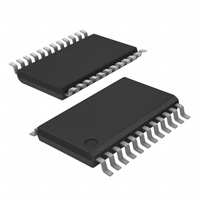
5 Pin Configuration and Functions
DB, DBQ, DGV, DW, OR PW PACKAGE
(TOP VIEW)
23
3
22
4
21
5
20
6
19
7
18
8
17
9
16
10
15
11
14
12
13
VCC
SDA
SCL
A0
P17
P16
P15
P14
P13
P12
P11
P10
SDA
SCL
24
2
RESET
A1
INT
VCC
1
24 23 22 21 20 19
P00
P01
P02
P03
P04
P05
1
2
3
18 A0
17 P17
16 P16
4
5
15 P15
14 P14
6
13 P13
7 8 9 10 11 12
P06
P07
GND
P10
P11
P12
INT
A1
RESET
P00
P01
P02
P03
P04
P05
P06
P07
GND
RGE PACKAGE
(TOP VIEW)
Table 5-1. Pin Functions
PIN
NO.
SOIC (DW),
SSOP (DB),
QSOP (DBQ),
TSSOP (PW), AND
TVSOP (DGV)
QFN (RGE)
INT
1
22
Interrupt output. Connect to VCC through a pullup resistor.
A1
2
23
Address input. Connect directly to VCC or ground.
RESET
3
24
Active-low reset input. Connect to VCC through a pullup resistor if no active
connection is used.
P00
4
1
P-port input/output. Push-pull design structure.
P01
5
2
P-port input/output. Push-pull design structure.
P02
6
3
P-port input/output. Push-pull design structure.
P03
7
4
P-port input/output. Push-pull design structure.
P04
8
5
P-port input/output. Push-pull design structure.
P05
9
6
P-port input/output. Push-pull design structure.
P06
10
7
P-port input/output. Push-pull design structure.
P07
11
8
P-port input/output. Push-pull design structure.
GND
12
9
Ground
P10
13
10
P-port input/output. Push-pull design structure.
NAME
4
DESCRIPTION
P11
14
11
P-port input/output. Push-pull design structure.
P12
15
12
P-port input/output. Push-pull design structure.
P13
16
13
P-port input/output. Push-pull design structure.
P14
17
14
P-port input/output. Push-pull design structure.
P15
18
15
P-port input/output. Push-pull design structure.
P16
19
16
P-port input/output. Push-pull design structure.
P17
20
17
P-port input/output. Push-pull design structure.
A0
21
18
Address input. Connect directly to VCC or ground.
SCL
22
19
Serial clock bus. Connect to VCC through a pullup resistor.
SDA
23
20
Serial data bus. Connect to VCC through a pullup resistor.
VCC
24
21
Supply voltage
Submit Document Feedback
Copyright © 2021 Texas Instruments Incorporated
Product Folder Links: PCA9539
�PCA9539
www.ti.com
SCPS130H – AUGUST 2005 – REVISED MARCH 2021
6 Specifications
6.1 Absolute Maximum Ratings
over operating free-air temperature range (unless otherwise noted) (1)
VCC
MIN
MAX
Supply voltage range
–0.5
6
UNIT
V
range(2)
–0.5
6
V
–0.5
6
V
VI
Input voltage
VO
Output voltage range(2)
IIK
Input clamp current
VI < 0
–20
mA
IOK
Output clamp current
VO < 0
–20
mA
±20
mA
50
mA
–50
mA
IIOK
Input/output clamp current
VO < 0 or VO > VCC
IOL
Continuous output low current
VO = 0 to VCC
IOH
Continuous output high current
VO = 0 to VCC
ICC
Tstg
(1)
(2)
Continuous current through GND
–250
Continuous current through VCC
160
Storage temperature range
-65
150
mA
°C
Stresses beyond those listed under "absolute maximum ratings" may cause permanent damage to the device. These are stress ratings
only, and functional operation of the device at these or any other conditions beyond those indicated under "recommended operating
conditions" is not implied. Exposure to absolute-maximum-rated conditions for extended periods may affect device reliability.
The input negative-voltage and output voltage ratings may be exceeded if the input and output current ratings are observed.
6.2 ESD Ratings
MIN
V(ESD)
(1)
(2)
Electrostatic discharge
MAX
UNIT
Human body model (HBM), per ANSI/ESDA/JEDEC JS-001, all
pins(1)
0
2000
Charged device model (CDM), per JEDEC specification
JESD22-C101, all pins(2)
0
1000
V
JEDEC document JEP155 states that 500-V HBM allows safe manufacturing with a standard ESD control process.
JEDEC document JEP157 states that 250-V CDM allows safe manufacturing with a standard ESD control process.
6.3 Recommended Operating Conditions
VCC
Supply voltage
VIH
High-level input voltage
VIL
Low-level input voltage
MIN
MAX
UNIT
2.3
VCC
V
SCL, SDA
0.7 × VCC
VCC
A0, A1, RESET, P07–P00, P17–P10
0.7 × VCC
5.5
SCL, SDA
–0.5
0.3 × VCC
A0, A1, RESET, P07–P00, P17–P10
–0.5
0.3 × VCC
V
V
IOH
High-level output current
P07–P00, P17–P10
–10
mA
IOL
Low-level output current
P07–P00, P17–P00
25
mA
TA
Operating free-air temperature
85
°C
–40
Submit Document Feedback
Copyright © 2021 Texas Instruments Incorporated
Product Folder Links: PCA9539
5
�PCA9539
www.ti.com
SCPS130H – AUGUST 2005 – REVISED MARCH 2021
6.4 Thermal Resistance Characteristics
PCA9539
THERMAL METRIC(1)
R θJA
Junction-to-ambient
thermal resistance
θ JP
Junction-to-pad
characterization parameter
(1)
DB
(SSOP)
DBQ
(SSOP)
DVG
(TVSOP)
DW
(SOIC)
PW
(TSSOP)
RGE
(VQFN)
24 Pins
24 Pins
24 Pins
24 Pins
24 Pins
24 Pins
63
61
86
46
108.8
48.4
°C/W
1.5
°C/W
UNIT
For more information about traditional and new thermal metrics, see the Semiconductor and IC package thermal metrics application
report.
6.5 Electrical Characteristics
over recommended operating free-air temperature range (unless otherwise noted)
PARAMETER
TEST CONDITIONS
VCC
MIN
–1.2
VIK
Input diode clamp voltage
II = –18 mA
2.3 V to 5.5 V
VPORR
Power-on reset voltage, VCC rising
VI = VCC or GND, IO = 0
2.3 V to 5.5 V
VPORF
Power-on reset voltage, VCC falling
VI = VCC or GND, IO = 0
2.3 V to 5.5 V
0.75
2.3 V
1.8
IOH = –8 mA
VOH
P-port high-level output voltage(2)
IOH = –10 mA
3V
2.6
4.75 V
4.1
2.3 V
1.7
3V
2.5
4.75 V
SDA
IOL
VOL = 0.5 V
VOL = 0.7 V
INT
II
A0, A1, RESET
(4)
2.3 V to 5.5 V
P port
VI = VCC
2.3 V to 5.5 V
IIL
P port
VI = GND
2.3 V to 5.5 V
VI = VCC or GND, IO = 0,
I/O = inputs, fSCL = 400 kHz
8
20
10
24
mA
±1
±1
μA
–1
μA
30
75
20
50
5.5 V
1.5
8.7
3.6 V
0.9
4
2.7 V
0.6
3
2.3 V to 5.5 V
Ci
SCL
VI = VCC or GND
2.3 V to 5.5 V
VIO = VCC or GND
2.3 V to 5.5 V
μA
1
2.7 V
Additional current in standby mode
(3)
(4)
V
3.6 V
ΔICC
(1)
(2)
V
V
200
One input at VCC – 0.6 V,
Other inputs at VCC or GND
P port
1
100
VI = GND, IO = 0, I/O = inputs,
fSCL = 0 kHz
SDA
V
5.5 V
Standby mode
Cio
1.5
3
VI = VCC or GND
ICC
6
2.3 V to 5.5 V
IIH
Operating mode
1.2
UNIT
3
VOL = 0.4 V
SCL, SDA
MAX
4
VOL = 0.4 V
P port(3)
TYP(1)
μA
200
μA
3
8
pF
3
9.5
3.7
9.5
pF
All typical values are at nominal supply voltage (2.5-V, 3.3-V, or 5-V VCC) and TA = 25°C.
Each I/O must be externally limited to a maximum of 25 mA, and each octal (P07–P00 and P17–P10) must be limited to a maximum
current of 100 mA, for a device total of 200 mA.
The total current sourced by all I/Os must be limited to 160 mA (80 mA for P07–P00 and 80 mA for P17–P10).
RESET = VCC (held high) when all other input voltages, VI = GND.
Submit Document Feedback
Copyright © 2021 Texas Instruments Incorporated
Product Folder Links: PCA9539
�PCA9539
www.ti.com
SCPS130H – AUGUST 2005 – REVISED MARCH 2021
6.6 I2C Interface Timing Requirements
over recommended operating free-air temperature range (unless otherwise noted) (see Figure 7-1)
MIN
MAX
UNIT
0
400
kHz
fscl
I2C
tsch
I2C clock high time
0.6
1.3
clock frequency
tscl
I2C
tsp
I2C spike time
clock low time
μs
μs
50
ns
tsds
I2C
tsdh
I2C serial-data hold time
ticr
I2C
ticf
I2C input fall time
tocf
I2C
tbuf
I2C bus free time between Stop and Start
1.3
μs
tsts
I2C Start or repeated Start condition setup
0.6
μs
tsth
I2C
0.6
μs
tsps
I2C Stop condition setup
0.6
μs
serial-data setup time
input rise time
output fall time
100
ns
0
ns
(1)
300
ns
20 + 0.1Cb (1)
300
ns
(1)
300
20 + 0.1Cb
10-pF to 400-pF bus
20 + 0.1Cb
Start or repeated Start condition hold
tvd(data)
Valid-data time
SCL low to SDA output valid
50
tvd(ack)
Valid-data time of ACK condition
ACK signal from SCL low to SDA (out) low
0.1
Cb
I2C bus capacitive load
(1)
ns
ns
0.9
μs
400
pF
Cb = total capacitance of one bus line in pF
6.7 RESET Timing Requirements
over recommended operating free-air temperature range (unless otherwise noted) (see Figure 7-4)
MIN
MAX
UNIT
tW
Reset pulse duration
6
ns
tREC
Reset recovery time
0
ns
tRESET
Time to reset
400
ns
6.8 Switching Characteristics
over recommended operating free-air temperature range, CL ≤ 100 pF (unless otherwise noted) (see Figure 7-2 and Figure
7-3)
PARAMETER
FROM
(INPUT)
TO
(OUTPUT)
P port
INT
4
μs
SCL
INT
4
μs
MIN
MAX
UNIT
tiv
Interrupt valid time
tir
Interrupt reset delay time
tpv
Output data valid
SCL
P port
tps
Input data setup time
P port
SCL
150
ns
tph
Input data hold time
P port
SCL
1
μs
200
ns
Submit Document Feedback
Copyright © 2021 Texas Instruments Incorporated
Product Folder Links: PCA9539
7
�PCA9539
www.ti.com
SCPS130H – AUGUST 2005 – REVISED MARCH 2021
6.9 Typical Characteristics
TA = 25°C (unless otherwise noted)
40
2.2
Vcc = 1.65 V
Vcc = 1.8 V
Vcc = 2.5 V
32
Vcc = 3.3 V
Vcc = 3.6 V
Vcc = 5 V
Vcc = 5.5V
28
24
20
16
12
8
0
-40
-15
10
35
TA - Temperature (°C)
60
Vcc = 5.5V
1.6
1.4
1.2
1
0.8
0.6
0.2
-40
85
-15
D001
Figure 6-1. Supply Current vs Temperature for
Different Supply Voltage (VCC)
10
35
TA - Temperature (°C)
60
85
D002
Figure 6-2. Standby Supply Current vs
Temperature for Different Supply Voltage (VCC)
30
30
-40qC
25qC
85qC
-40qC
25qC
85qC
25
IOL - Sink Current (mA)
25
ICC - Supply Current (µA)
1.8
Vcc = 3.3 V
Vcc = 3.6 V
Vcc = 5 V
0.4
4
20
15
10
5
20 VCC = 1.65 V
15
10
5
0
1.5
0
2
2.5
3
3.5
4
4.5
VCC - Supply Voltage (V)
5
5.5
0
0.1
D003
Figure 6-3. Supply Current vs Supply Voltage for
Different Temperature (TA)
0.2
0.3
0.4
0.5
VOL - Output Low Voltage (V)
0.6
0.7
D004
Figure 6-4. I/O Sink Current vs Output Low Voltage
for Different Temperature (TA) for VCC = 1.65 V
60
35
25
IOL - Sink Current (mA)
-40qC
25qC
85qC
30
IOL - Sink Current (mA)
Vcc = 1.65 V
Vcc = 1.8 V
Vcc = 2.5 V
2
ICC - Supply Current (µA)
ICC - Supply Current (µA)
36
VCC = 1.8 V
20
15
10
50
-40qC
25qC
85qC
40
VCC = 2.5 V
30
20
10
5
0
0
0
0.1
0.2
0.3
0.4
0.5
VOL - Output Low Voltage (V)
0.6
0.7
0
D005
0.1
0.2
0.3
0.4
0.5
VOL - Output Low Voltage (V)
0.6
0.7
D006
Figure 6-5. I/O Sink Current vs Output Low Voltage Figure 6-6. I/O Sink Current vs Output Low Voltage
for Different Temperature (TA) for VCC = 1.8 V
for Different Temperature (TA) for VCC = 2.5 V
8
Submit Document Feedback
Copyright © 2021 Texas Instruments Incorporated
Product Folder Links: PCA9539
�PCA9539
www.ti.com
SCPS130H – AUGUST 2005 – REVISED MARCH 2021
70
80
-40qC
25qC
85qC
50
-40qC
25qC
85qC
70
IOL - Sink Current (mA)
IOL - Sink Current (mA)
60
VCC = 3.3 V
40
30
20
10
60
VCC = 5 V
50
40
30
20
10
0
0
0
0.1
0.2
0.3
0.4
0.5
VOL - Output Low Voltage (V)
0.6
0.7
0
0.1
0.2
0.3
0.4
0.5
VOL - Output Low Voltage (V)
D007
0.6
0.7
D009
Figure 6-7. I/O Sink Current vs Output Low Voltage Figure 6-8. I/O Sink Current vs Output Low Voltage
for Different Temperature (TA) for VCC = 3.3 V
for Different Temperature (TA) for VCC = 5 V
300
90
IOL - Sink Current (mA)
80
70
VOL - Output Low Voltage (V)
-40qC
25qC
85qC
VCC = 5.5 V
60
50
40
30
20
1.8 V, 1 mA
1.8 V, 10 mA
3.3 V, 1mA
250
3.3 V, 10 mA
5 V, 1 mA
5 V, 10 mA
200
150
100
50
10
0
-40
0
0
0.1
0.2
0.3
0.4
0.5
VOL - Output Low Voltage (V)
0.6
0.7
Figure 6-9. I/O Sink Current vs Output Low Voltage
for Different Temperature (TA) for VCC = 5.5 V
10
35
TA - Temperature (°C)
60
85
D011
Figure 6-10. II/O Low Voltage vs Temperature for
Different VCC and IOL
20
25
-40qC
25qC
85qC
IOH - Source Current (mA)
IOH - Source Current (mA)
-15
D010
15
VCC = 1.65 V
10
5
0
-40qC
25qC
85qC
20
VCC = 1.8 V
15
10
5
0
0
0.1
0.2
0.3
0.4
0.5
VCC-VOH - Output High Voltage (V)
0.6
0.7
0
D012
Figure 6-11. I/O Source Current vs Output High
Voltage for Different Temperature (TA) for VCC =
1.65 V
0.1
0.2
0.3
0.4
0.5
VCC-VOH - Output High Voltage (V)
0.6
0.7
D013
Figure 6-12. I/O Source Current vs Output High
Voltage for Different Temperature (TA) for VCC = 1.8
V
Submit Document Feedback
Copyright © 2021 Texas Instruments Incorporated
Product Folder Links: PCA9539
9
�PCA9539
www.ti.com
SCPS130H – AUGUST 2005 – REVISED MARCH 2021
60
40
IOH - Source Current (mA)
35
IOH - Source Current (mA)
-40qC
25qC
85qC
30
VCC = 2.5 V
25
20
15
10
50
-40qC
25qC
85qC
40
VCC = 3.3 V
30
20
10
5
0
0
0
0.1
0.2
0.3
0.4
0.5
VCC-VOH - Output High Voltage (V)
0.6
0.7
0
0.1
0.2
0.3
0.4
0.5
VCC-VOH - Output High Voltage (V)
D014
0.6
0.7
D015
Figure 6-13. I/O Source Current vs Output High
Figure 6-14. I/O Source Current vs Output High
Voltage for Different Temperature (TA) for VCC = 2.5 Voltage for Different Temperature (TA) for VCC = 3.3
V
V
70
80
-40qC
25qC
85qC
50
-40qC
25qC
85qC
70
IOH - Source Current (mA)
IOH - Source Current (mA)
60
VCC = 5 V
40
30
20
10
60
VCC = 5.5 V
50
40
30
20
10
0
0
0
0.1
0.2
0.3
0.4
0.5
VCC-VOH - Output High Voltage (V)
0.6
0.7
0
D016
0.1
0.2
0.3
0.4
0.5
VCC-VOH - Output High Voltage (V)
0.6
0.7
D017
Figure 6-15. I/O Source Current vs Output High
Figure 6-16. I/O Source Current vs Output High
Voltage for Different Temperature (TA) for VCC = 5 V Voltage for Different Temperature (TA) for VCC = 5.5
V
350
18
1.65 V, 10 mA
2.5 V, 10 mA
3.6 V, 10 mA
5 V, 10 mA
5.5 V, 10 mA
15
250
200
150
3.3 V
5V
5.5 V
12
9
6
3
100
50
-40
-15
10
35
TA - Temperature (°C)
60
85
0
-40
D018
Figure 6-17. VCC – VOH Voltage vs Temperature for
Different VCC
10
1.65 V
1.8 V
2.5 V
300
Delta ICC (µA)
VCC-VOH - I/O High Voltage (mV)
400
-15
10
35
TA - Temperature (°C)
60
85
D019
Figure 6-18. Δ ICC vs Temperature for Different VCC
(VI = VCC – 0.6 V)
Submit Document Feedback
Copyright © 2021 Texas Instruments Incorporated
Product Folder Links: PCA9539
�PCA9539
www.ti.com
SCPS130H – AUGUST 2005 – REVISED MARCH 2021
7 Parameter Measurement Information
VCC
RL = 1 kΩ
SDA
DUT
CL = 50 pF
(see Note A)
SDA LOAD CONFIGURATION
Three Bytes for Complete
Device Programming
Stop
Condition
(P)
Start
Address
Address
Condition
Bit 7
Bit 6
(S)
(MSB)
Address
Bit 1
tscl
R/W
Bit 0
(LSB)
ACK
(A)
Data
Bit 7
(MSB)
Data
Bit 0
(LSB)
Stop
Condition
(P)
tsch
0.7 × VCC
SCL
0.3 × VCC
ticr
tPHL
ticf
tbuf
tsts
tPLH
tsp
0.7 × VCC
SDA
0.3 × VCC
ticf
ticr
tsth
tsdh
tsds
tsps
Repeat
Start
Condition
Start or
Repeat
Start
Condition
Stop
Condition
VOLTAGE WAVEFORMS
BYTE
DESCRIPTION
1
I2C address
2, 3
P-port data
A. CL includes probe and jig capacitance.
B. All inputs are supplied by generators having the following characteristics: PRR ≤ 10 MHz, ZO = 50 Ω, tr/tf ≤ 30 ns.
C. All parameters and waveforms are not applicable to all devices.
Figure 7-1. I2C Interface Load Circuit And Voltage Waveforms
Submit Document Feedback
Copyright © 2021 Texas Instruments Incorporated
Product Folder Links: PCA9539
11
�PCA9539
www.ti.com
SCPS130H – AUGUST 2005 – REVISED MARCH 2021
VCC
RL = 4.7 kΩ
INT
DUT
CL = 100 pF
(see Note A)
INTERRUPT LOAD CONFIGURATION
ACK
From Slave
Start
Condition
8 Bits
(One Data Byte)
From Port
R/W
Slave Address
S
1
1
1
0
1
1
2
3
4
5
A1 A0 1
6
7
8
Data 1
A
ACK
From Slave
Data From Port
A
Data 2
1
P
A
A
tir
tir
B
B
INT
A
tiv
tsps
A
Data
Into
Port
Address
Data 1
0.7 × VCC
INT
SCL
0.3 × VCC
Data 2
0.7 × VCC
R/W
tiv
A
0.3 × VCC
tir
0.7 × VCC
Pn
0.7 × VCC
INT
0.3 × VCC
0.3 × VCC
View A−A
View B−B
A. CL includes probe and jig capacitance.
B. All inputs are supplied by generators having the following characteristics: PRR ≤ 10 MHz, ZO = 50 Ω, tr/tf ≤ 30 ns.
C. All parameters and waveforms are not applicable to all devices.
Figure 7-2. Interrupt Load Circuit And Voltage Waveforms
12
Submit Document Feedback
Copyright © 2021 Texas Instruments Incorporated
Product Folder Links: PCA9539
�PCA9539
www.ti.com
SCPS130H – AUGUST 2005 – REVISED MARCH 2021
500 W
Pn
DUT
2 × VCC
CL = 50 pF
(see Note A)
500 W
P-PORT LOAD CONFIGURATION
0.7 × VCC
SCL
P0
A
P3
0.3 × VCC
Slave
ACK
ÎÎÎ
ÎÎÎ
ÎÎÎ
ÎÎÎ
ÎÎÎ
SDA
Pn
tpv
(see Note B)
Unstable
Data
Last Stable Bit
WRITE MODE (R/W = 0)
0.7 × VCC
SCL
P0
A
tps
P3
0.3 × VCC
tph
0.7 × VCC
Pn
0.3 × VCC
READ MODE (R/W = 1)
A.
B.
C.
D.
E.
CL includes probe and jig capacitance.
tpv is measured from 0.7 × VCC on SCL to 50% I/O (Pn) output.
All inputs are supplied by generators having the following characteristics: PRR ≤ 10 MHz, ZO = 50 Ω, tr/tf ≤ 30 ns.
The outputs are measured one at a time, with one transition per measurement.
All parameters and waveforms are not applicable to all devices.
Figure 7-3. P-Port Load Circuit And Voltage Waveforms
Submit Document Feedback
Copyright © 2021 Texas Instruments Incorporated
Product Folder Links: PCA9539
13
�PCA9539
www.ti.com
SCPS130H – AUGUST 2005 – REVISED MARCH 2021
VCC
Pn
RL = 1 kΩ
DUT
500 W
DUT
SDA
2 × VCC
CL = 50 pF
(see Note A)
500 W
CL = 50 pF
(see Note A)
SDA LOAD CONFIGURATION
P-PORT LOAD CONFIGURATION
Start
SCL
ACK or Read Cycle
SDA
0.3 y VCC
tRESET
RESET
VCC/2
tREC
tw
Pn
VCC/2
tRESET
A.
B.
C.
D.
E.
CL includes probe and jig capacitance.
All inputs are supplied by generators having the following characteristics: PRR ≤ 10 MHz, ZO = 50 Ω, tr/tf ≤ 30 ns.
The outputs are measured one at a time, with one transition per measurement.
I/Os are configured as inputs.
All parameters and waveforms are not applicable to all devices.
Figure 7-4. Reset Load Circuits And Voltage Waveforms
14
Submit Document Feedback
Copyright © 2021 Texas Instruments Incorporated
Product Folder Links: PCA9539
�PCA9539
www.ti.com
SCPS130H – AUGUST 2005 – REVISED MARCH 2021
8 Detailed Description
8.1 Functional Block Diagram
INT
A0
A1
SCL
SDA
PCA9539
1
Interrupt
Logic
LP Filter
21
2
P07−P00
22
23
I2C Bus
Control
Input
Filter
Shift
Register
16 Bits
I/O
Port
P17−P10
RESET
VCC
GND
Write Pulse
3
24
12
Power-On
Reset
Read Pulse
A. Pin numbers shown are for DB, DBQ, DGV, DW, and PW packages.
B. All I/Os are set to inputs at reset.
Figure 8-1. Logic Diagram (Positive Logic)
Submit Document Feedback
Copyright © 2021 Texas Instruments Incorporated
Product Folder Links: PCA9539
15
�PCA9539
www.ti.com
SCPS130H – AUGUST 2005 – REVISED MARCH 2021
Data From
Shift Register
Output Port
Register Data
Configuration
Register
Data From
Shift Register
D
Q
FF
Write Configuration
Pulse
VCC
Q1
D
CLK Q
Write Pulse
Q
FF
I/O Pin
CLK Q
Output Port
Register
Q2
Input Port
Register
D
GND
Q
Input Port
Register Data
FF
Read Pulse
CLK Q
To INT
Data From
Shift Register
D
Polarity
Register Data
Q
FF
Write Polarity
Pulse
CLK Q
Polarity Inversion
Register
A. At power-on reset, all registers return to default values.
Figure 8-2. Simplified Schematic Of P-Port I/Os
16
Submit Document Feedback
Copyright © 2021 Texas Instruments Incorporated
Product Folder Links: PCA9539
�PCA9539
www.ti.com
SCPS130H – AUGUST 2005 – REVISED MARCH 2021
8.2 Device Functional Modes
8.2.1 RESET Input
A reset can be accomplished by holding the RESET pin low for a minimum of tW. The PCA9539 registers and
I2C/SMBus state machine are held in their default states until RESET is once again high. This input requires a
pullup resistor to VCC, if no active connection is used.
8.2.1.1 RESET Errata
If RESET voltage set higher than VCC, current will flow from RESET pin to VCC pin.
8.2.1.1.1 System Impact
VCC will be pulled above its regular voltage level
8.2.1.1.2 System Workaround
Design such that RESET voltage is same or lower than VCC
8.2.2 Power-On Reset
When power (from 0 V) is applied to VCC, an internal power-on reset holds the PCA9539 in a reset condition until
VCC has reached VPOR. At that point, the reset condition is released and the PCA9539 registers and I2C/SMBus
state machine initialize to their default states. After that, VCC must be lowered to below 0.2 V and then back up to
the operating voltage for a power-reset cycle.
8.2.3 I/O Port
When an I/O is configured as an input, FETs Q1 and Q2 (in Figure 8-2) are off, which creates a high-impedance
input. The input voltage may be raised above VCC to a maximum of 5.5 V.
If the I/O is configured as an output, Q1 or Q2 is enabled, depending on the state of the Output Port register.
In this case, there are low-impedance paths between the I/O pin and either VCC or GND. The external voltage
applied to this I/O pin should not exceed the recommended levels for proper operation.
8.2.4 Interrupt ( INT) Output
An interrupt is generated by any rising or falling edge of the port inputs in the input mode. After time, tiv,
the signal INT is valid. Resetting the interrupt circuit is achieved when data on the port is changed to the
original setting, data is read from the port that generated the interrupt. Resetting occurs in the read mode at the
acknowledge (ACK) or not acknowledge (NACK) bit after the rising edge of the SCL signal.
Interrupts that occur during the ACK or NACK clock pulse can be lost (or be very short) due to the resetting
of the interrupt during this pulse. Each change of the I/Os after resetting is detected and is transmitted as INT.
Writing to another device does not affect the interrupt circuit, and a pin configured as an output cannot cause
an interrupt. Changing an I/O from an output to an input may cause a false interrupt to occur, if the state of the
pin does not match the contents of the Input Port register. Because each 8-pin port is read independently, the
interrupt caused by port 0 is not cleared by a read of port 1 or vice versa.
The INT output has an open-drain structure and requires pullup resistor to VCC.
Submit Document Feedback
Copyright © 2021 Texas Instruments Incorporated
Product Folder Links: PCA9539
17
�PCA9539
www.ti.com
SCPS130H – AUGUST 2005 – REVISED MARCH 2021
8.2.4.1 Interrupt Errata
The INT will be improperly de-asserted if the following two conditions occur:
1. The last I2C command byte (register pointer) written to the device was 00h.
Note
This generally means the last operation with the device was a Read of the input register. However,
the command byte may have been written with 00h without ever going on to read the input register.
After reading from the device, if no other command byte written, it will remain 00h.
2. Any other slave device on the I2C bus acknowledges an address byte with the R/W bit set high
8.2.4.1.1 System Impact
Can cause improper interrupt handling as the Master will see the interrupt as being cleared.
8.2.4.1.2 System Workaround
Minor software change: User must change command byte to something besides 00h after a Read operation to
the PCA9539 device or before reading from another slave device.
Note
Software change will be compatible with other versions (competition and TI redesigns) of this device.
8.3 Programming
8.3.1 I2C Interface
The bidirectional I2C bus consists of the serial clock (SCL) and serial data (SDA) lines. Both lines must be
connected to a positive supply via a pullup resistor when connected to the output stages of a device. Data
transfer may be initiated only when the bus is not busy.
I2C communication with this device is initiated by a master sending a Start condition, a high-to-low transition on
the SDA input/output while the SCL input is high (see Figure 8-3). After the Start condition, the device address
byte is sent, MSB first, including the data direction bit (R/ W). This device does not respond to the general call
address.
After receiving the valid address byte, this device responds with an ACK, a low on the SDA input/output during
the high of the ACK-related clock pulse. The address inputs (A0 and A1) of the slave device must not be
changed between the Start and Stop conditions.
On the I2C bus, only one data bit is transferred during each clock pulse. The data on the SDA line must remain
stable during the high pulse of the clock period, as changes in the data line at this time are interpreted as control
commands (Start or Stop) (see Figure 8-4).
A Stop condition, a low-to-high transition on the SDA input/output while the SCL input is high, is sent by the
master (see Figure 8-3).
Any number of data bytes can be transferred from the transmitter to the receiver between the Start and the Stop
conditions. Each byte of eight bits is followed by one ACK bit. The transmitter must release the SDA line before
the receiver can send an ACK bit. The device that acknowledges must pull down the SDA line during the ACK
clock pulse so that the SDA line is stable low during the high pulse of the ACK-related clock period (see Figure
8-5). When a slave receiver is addressed, it must generate an ACK after each byte is received. Similarly, the
master must generate an ACK after each byte that it receives from the slave transmitter. Setup and hold times
must be met to ensure proper operation.
A master receiver signals an end of data to the slave transmitter by not generating an acknowledge (NACK) after
the last byte has been clocked out of the slave. This is done by the master receiver by holding the SDA line high.
In this event, the transmitter must release the data line to enable the master to generate a Stop condition.
18
Submit Document Feedback
Copyright © 2021 Texas Instruments Incorporated
Product Folder Links: PCA9539
�PCA9539
www.ti.com
SCPS130H – AUGUST 2005 – REVISED MARCH 2021
SDA
SCL
S
P
Start Condition
Stop Condition
Figure 8-3. Definition Of Start And Stop Conditions
SDA
SCL
Data Line
Stable;
Data Valid
Change
of Data
Allowed
Figure 8-4. Bit Transfer
Data Output
by Transmitter
NACK
Data Output
by Receiver
ACK
SCL From
Master
1
2
8
9
S
Clock Pulse for
Acknowledgment
Start
Condition
Figure 8-5. Acknowledgment On I2C Bus
8.3.2 Register Map
Table 8-1. Interface Definition
BYTE
BIT
7 (MSB)
6
5
4
3
2
1
0 (LSB)
I2C slave address
H
H
H
L
H
A1
A0
R/ W
P0x I/O data bus
P07
P06
P05
P04
P03
P02
P01
P00
P1x I/O data bus
P17
P16
P15
P14
P13
P12
P11
P10
Submit Document Feedback
Copyright © 2021 Texas Instruments Incorporated
Product Folder Links: PCA9539
19
�PCA9539
www.ti.com
SCPS130H – AUGUST 2005 – REVISED MARCH 2021
8.3.2.1 Device Address
Figure 8-6 shows the address byte of the PCA9539.
R/W
Slave Address
1
1
1
0
Fixed
1
A1 A0
Programmable
Figure 8-6. Pca9539 Address
Table 8-2. Address Reference
INPUTS
A1
I2C BUS SLAVE ADDRESS
A0
L
L
116 (decimal), 74 (hexadecimal)
L
H
117 (decimal), 75 (hexadecimal)
H
L
118 (decimal), 76 (hexadecimal)
H
H
119 (decimal), 77 (hexadecimal)
The last bit of the slave address defines the operation (read or write) to be performed. A high (1) selects a read
operation, while a low (0) selects a write operation.
8.3.2.2 Control Register And Command Byte
Following the successful acknowledgment of the address byte, the bus master sends a command byte that is
stored in the control register in the PCA9539. Three bits of this data byte state the operation (read or write) and
the internal register (input, output, Polarity Inversion or Configuration) that will be affected. This register can be
written or read through the I2C bus. The command byte is sent only during a write transmission.
Once a command byte has been sent, the register that was addressed continues to be accessed by reads until a
new command byte has been sent.
0
0
0
0
0
B2
B1
B0
Figure 8-7. Control Register Bits
Table 8-3. Command Byte
CONTROL REGISTER BITS
B2
20
B1
B0
COMMAND
BYTE (HEX)
REGISTER
PROTOCOL
POWER-UP
DEFAULT
0
0
0
0x00
Input Port 0
Read byte
xxxx xxxx
0
0
1
0x01
Input Port 1
Read byte
xxxx xxxx
0
1
0
0x02
Output Port 0
Read/write byte
1111 1111
0
1
1
0x03
Output Port 1
Read/write byte
1111 1111
1
0
0
0x04
Polarity Inversion Port 0
Read/write byte
0000 0000
1
0
1
0x05
Polarity Inversion Port 1
Read/write byte
0000 0000
1
1
0
0x06
Configuration Port 0
Read/write byte
1111 1111
1
1
1
0x07
Configuration Port 1
Read/write byte
1111 1111
Submit Document Feedback
Copyright © 2021 Texas Instruments Incorporated
Product Folder Links: PCA9539
�PCA9539
www.ti.com
SCPS130H – AUGUST 2005 – REVISED MARCH 2021
8.3.2.3 Register Descriptions
The Input Port registers (registers 0 and 1) reflect the incoming logic levels of the pins, regardless of whether
the pin is defined as an input or an output by the Configuration register. It only acts on read operation. Writes to
these registers have no effect. The default value, X, is determined by the externally applied logic level.
Before a read operation, a write transmission is sent with the command byte to indicate to the I2C device that the
Input Port register will be accessed next.
Table 8-4. Registers 0 And 1 (Input Port Registers)
Bit
I0.7
Default
Bit
Default
I0.6
I0.5
I0.4
I0.3
I0.2
I0.1
I0.0
X
X
X
X
X
X
X
X
I1.7
I1.6
I1.5
I1.4
I1.3
I1.2
I1.1
I1.0
X
X
X
X
X
X
X
X
The Output Port registers (registers 2 and 3) show the outgoing logic levels of the pins defined as outputs by the
Configuration register. Bit values in this register have no effect on pins defined as inputs. In turn, reads from this
register reflect the value that is in the flip-flop controlling the output selection, not the actual pin value.
Table 8-5. Registers 2 And 3 (Output Port Registers)
Bit
O0.7
Default
Bit
Default
O0.6
O0.5
O0.4
O0.3
O0.2
O0.1
O0.0
1
1
1
1
1
1
1
1
O1.7
O1.6
O1.5
O1.4
O1.3
O1.2
O1.1
O1.0
1
1
1
1
1
1
1
1
The Polarity Inversion registers (registers 4 and 5) allow Polarity Inversion of pins defined as inputs by the
Configuration register. If a bit in this register is set (written with 1), the corresponding port pin's polarity is
inverted. If a bit in this register is cleared (written with a 0), the corresponding port pin's original polarity is
retained.
Table 8-6. Registers 4 And 5 (Polarity Inversion Registers)
Bit
Default
Bit
Default
N0.7
N0.6
N0.5
N0.4
N0.3
N0.2
N0.1
N0.0
0
0
0
0
0
0
0
0
N1.7
N1.6
N1.5
N1.4
N1.3
N1.2
N1.1
N1.0
0
0
0
0
0
0
0
0
The Configuration registers (registers 6 and 7) configure the directions of the I/O pins. If a bit in this register is
set to 1, the corresponding port pin is enabled as an input with a high-impedance output driver. If a bit in this
register is cleared to 0, the corresponding port pin is enabled as an output.
Table 8-7. Registers 6 And 7 (Configuration Registers)
Bit
Default
Bit
Default
C0.7
C0.6
C0.5
C0.4
C0.3
C0.2
C0.1
C0.0
1
1
1
1
1
1
1
1
C1.7
C1.6
C1.5
C1.4
C1.3
C1.2
C1.1
C1.0
1
1
1
1
1
1
1
1
8.3.2.4 Bus Transactions
Data is exchanged between the master and PCA9539 through write and read commands.
8.3.2.4.1 Writes
Data is transmitted to the PCA9539 by sending the device address and setting the least-significant bit to a
logic 0 (see Figure 8-6 for device address). The command byte is sent after the address and determines which
register receives the data that follows the command byte.
Submit Document Feedback
Copyright © 2021 Texas Instruments Incorporated
Product Folder Links: PCA9539
21
�PCA9539
www.ti.com
SCPS130H – AUGUST 2005 – REVISED MARCH 2021
The eight registers within the PCA9539 are configured to operate as four register pairs. The four pairs are Input
Ports, Output Ports, Polarity Inversion ports, and Configuration ports. After sending data to one register, the next
data byte is sent to the other register in the pair (see Figure 8-8 and Figure 8-9). For example, if the first byte is
sent to Output Port 1 (register 3), the next byte is stored in Output Port 0 (register 2).
There is no limitation on the number of data bytes sent in one write transmission. In this way, each 8-bit register
may be updated independently of the other registers.
1
SCL
2
3
4
5
6
7
8
9
Command Byte
Slave Address
SDA
S
1
1
1
0
1
A1 A0
0
0
A
0
0
0
0
0
Data to Port 0
1
A 0.7
0
R/W Acknowledge
From Slave
Start Condition
Data to Port 1
0.0
Data 0
Acknowledge
From Slave
A 1.7
1.0
Data 1
A
P
Acknowledge
From Slave
Write to Port
Data Out from Port 0
tpv
Data Valid
Data Out from Port 1
tpv
Figure 8-8. Write To Output Port Registers
1
SCL
2
3
4
5
6
7
8
9
1
2
3
Slave Address
SDA
S
1
1
1
Start Condition
0
1
4
5
6
7
8
9
1
2
3
0
R/W
A
0
0
0
Acknowledge
From Slave
0
0
1
1
5
6
7
8
9
1
2
3
Data to Register
Command Byte
A1 A0
4
0
A MSB
Data 0
4
5
Data to Register
LSB
Acknowledge
From Slave
A MSB
Data 1
LSB
A
P
Acknowledge
From Slave
Figure 8-9. Write To Configuration Registers
8.3.2.4.2 Reads
The bus master first must send the PCA9539 address with the least-significant bit set to a logic 0 (see Figure
8-6 for device address). The command byte is sent after the address and determines which register is accessed.
After a restart, the device address is sent again, but this time, the least-significant bit is set to a logic 1. Data
from the register defined by the command byte then is sent by the PCA9539 (see Figure 8-10 through Figure
8-12).
After a restart, the value of the register defined by the command byte matches the register being accessed when
the restart occurred. For example, if the command byte references Input Port 1 before the restart, and the restart
occurs when Input Port 0 is being read, the stored command byte changes to reference Input Port 0. The original
command byte is forgotten. If a subsequent restart occurs, Input Port 0 is read first. Data is clocked into the
register on the rising edge of the ACK clock pulse. After the first byte is read, additional bytes may be read, but
the data now reflect the information in the other register in the pair. For example, if Input Port 1 is read, the next
byte read is Input Port 0.
Data is clocked into the register on the rising edge of the ACK clock pulse. There is no limitation on the number
of data bytes received in one read transmission, but when the final byte is received, the bus master must not
acknowledge the data.
22
Submit Document Feedback
Copyright © 2021 Texas Instruments Incorporated
Product Folder Links: PCA9539
�PCA9539
www.ti.com
SCPS130H – AUGUST 2005 – REVISED MARCH 2021
Slave Address
S
1
1
1
0
1
Acknowledge
From Slave
A1 A0
0
Slave Address
Acknowledge
From Slave
A
A
Command Byte
S
R/W
1
1
1
0
1
Data From Lower
or Upper Byte
of Register
Acknowledge
From Slave
A1 A0
1
A MSB
LSB
Data
A
First Byte
R/W
At this moment, master
transmitter becomes master
receiver, and slave receiver
becomes slave transmitter.
Acknowledge
From Master
Data From Upper
or Lower Byte
of Register
MSB
No Acknowledge
From Master
LSB NA
Data
P
Last Byte
Figure 8-10. Read From Register
1
SCL
2
3
4
5
6
7
8
9
I0.x
SDA
S
1
1
1
0
1
A1
A0
1
R/W
A
7
6
5
4
Acknowledge
From Slave
3
I1.x
2
1
0
A
7
6
5
Acknowledge
From Master
4
3
I0.x
2
1
0
A
7
6
5
4
3
I1.x
2
Acknowledge
From Master
1
0
A
7
6
5
Acknowledge
From Master
4
3
2
1
0
1
P
No Acknowledge
From Master
Read From Port 0
Data Into Port 0
Read From Port 1
Data Into Port 1
INT
tiv
tir
A. Transfer of data can be stopped at any time by a Stop condition. When this occurs, data present at the latest acknowledge phase is valid
(output mode). It is assumed that the command byte previously has been set to 00 (Read Input Port register).
B. This figure eliminates the command byte transfer, a restart, and slave address call between the initial slave address call and actual data
transfer from the P port (see Figure 8-10 for these details).
Figure 8-11. Read Input Port Register, Scenario 1
Submit Document Feedback
Copyright © 2021 Texas Instruments Incorporated
Product Folder Links: PCA9539
23
�PCA9539
www.ti.com
SCPS130H – AUGUST 2005 – REVISED MARCH 2021
1
SCL
2
3
4
5
6
7
8
9
I0.x
SDA
S
1
1
1
0
1
A1
A0
1
R/W
A
00
Acknowledge
From Slave
I1.x
A
10
I0.x
A
I1.x
03
A
Acknowledge
From Master
Acknowledge
From Master
12
P
No Acknowledge
From Master
tps
tph
1
Acknowledge
From Master
Read From Port 0
Data Into Port 0
Data 00
Data 01
Data 02
Data 03
tph
Read From Port 1
Data 10
Data Into Port 1
tps
Data 11
Data 12
INT
tiv
tir
A. Transfer of data can be stopped at any time by a Stop condition. When this occurs, data present at the latest acknowledge phase is valid
(output mode). It is assumed that the command byte previously has been set to 00 (Read Input Port register).
B. This figure eliminates the command byte transfer, a restart, and slave address call between the initial slave address call and actual data
transfer from the P port (see Figure 8-10 for these details).
Figure 8-12. Read Input Port Register, Scenario 2
24
Submit Document Feedback
Copyright © 2021 Texas Instruments Incorporated
Product Folder Links: PCA9539
�PCA9539
www.ti.com
SCPS130H – AUGUST 2005 – REVISED MARCH 2021
9 Application Information Disclaimer
Note
Information in the following applications sections is not part of the TI component specification,
and TI does not warrant its accuracy or completeness. TI’s customers are responsible for
determining suitability of components for their purposes, as well as validating and testing their design
implementation to confirm system functionality.
9.1 Application Information
Figure 9-1 shows an application in which the PCA9539 can be used.
9.2 Typical Application
Subsystem 1
(e.g., Temperature
Sensor)
INT
VCC
(5 V)
10 kW
VCC
10 kW
10 kW
SCL
Master
Controller SDA
INT
GND
24
10 kW
22
23
2 kW
VCC
SCL
SDA
1
3 INT
RESET
Subsystem 2
(e.g., Counter)
100 kW
4
P00
5
P01
6
P02
7
P03
8
P04
9
P05
100 kW
100 kW
RESET
A
ENABLE
B
PCA9539
P06
P07
P10
P11
2
A1
P12
P13
21
A0
P14
P15
P16
GND P17
12
A.
B.
C.
D.
10
11
13
14
15
16
17
18
19
20
VCC
Controlled Switch
(e.g., CBT Device)
ALARM
Keypad
Subsystem 3
(e.g., Alarm)
Device address is configured as 1110100 for this example.
P00, P02, and P03 are configured as outputs.
P01 and P04 to P17 are configured as inputs.
Pin numbers shown are for DB, DBQ, DGV, DW, and PW packages.
Figure 9-1. Typical Application
Submit Document Feedback
Copyright © 2021 Texas Instruments Incorporated
Product Folder Links: PCA9539
25
�PCA9539
www.ti.com
SCPS130H – AUGUST 2005 – REVISED MARCH 2021
9.2.1 Detailed Design Procedure
9.2.1.1 Minimizing ICC When I/O Is Used To Control Led
When an I/O is used to control an LED, normally it is connected to VCC through a resistor (see Figure 9-1).
Because the LED acts as a diode, when the LED is off, the I/O VIN is about 1.2 V less than VCC. The
ΔICC parameter in Electrical Characteristics shows how ICC increases as VIN becomes lower than VCC. For
battery-powered applications, it is essential that the voltage of I/O pins is greater than or equal to VCC, when the
LED is off, to minimize current consumption.
Figure 9-2 shows a high-value resistor in parallel with the LED. Figure 9-3 shows VCC less than the LED supply
voltage by at least 1.2 V. Both of these methods maintain the I/O VCC at or above VCC and prevent additional
supply-current consumption when the LED is off.
VCC
LED
100 kW
VCC
Pn
Figure 9-2. High-Value Resistor In Parallel With Led
3.3 V
VCC
5V
LED
Pn
Figure 9-3. Device Supplied By Lower Voltage
26
Submit Document Feedback
Copyright © 2021 Texas Instruments Incorporated
Product Folder Links: PCA9539
�PCA9539
www.ti.com
SCPS130H – AUGUST 2005 – REVISED MARCH 2021
10 Power Supply Recommendations
10.1 Power-On Reset Requirements
In the event of a glitch or data corruption, PCA9539 can be reset to its default conditions by using the power-on
reset feature. Power-on reset requires that the device go through a power cycle to be completely reset. This
reset also happens when the device is powered on for the first time in an application.
The two types of power-on reset are shown in Figure 10-1 and Figure 10-2.
VCC
Ramp-Up
Re-Ramp-Up
Ramp-Down
VCC_TRR_GND
Time
VCC_RT
VCC_FT
Time to Re-Ramp
VCC_RT
Figure 10-1. VCC Is Lowered Below 0.2 V Or 0 V And Then Ramped Up To VCC
VCC
Ramp-Down
Ramp-Up
VCC_TRR_VPOR50
VIN drops below POR levels
Time
Time to Re-Ramp
VCC_FT
VCC_RT
Figure 10-2. VCC Is Lowered Below The Por Threshold, Then Ramped Back Up To VCC
Table 10-1 specifies the performance of the power-on reset feature for PCA9539 for both types of power-on
reset.
Table 10-1. Recommended Supply Sequencing And Ramp Rates (1)
PARAMETER
MIN
TYP
MAX
UNIT
VCC_FT
Fall rate
See Figure 10-1
1
100
ms
VCC_RT
Rise rate
See Figure 10-1
0.01
100
ms
VCC_TRR_GND
Time to re-ramp (when VCC drops to GND)
See Figure 10-1
0.001
ms
VCC_TRR_POR50
Time to re-ramp (when VCC drops to VPOR_MIN – 50 mV)
See Figure 10-2
0.001
ms
VCC_GH
Level that VCCP can glitch down to, but not cause a functional
disruption when VCCX_GW = 1 μs
See Figure 10-3
VCC_GW
Glitch width that will not cause a functional disruption when
VCCX_GH = 0.5 × VCCx
See Figure 10-3
VPORF
Voltage trip point of POR on falling VCC
0.767
1.144
V
VPORR
Voltage trip point of POR on rising VCC
1.033
1.428
V
(1)
1.2
V
μs
TA = –40°C to 85°C (unless otherwise noted)
Glitches in the power supply can also affect the power-on reset performance of this device. The glitch width
(VCC_GW) and height (VCC_GH) are dependent on each other. The bypass capacitance, source impedance, and
the device impedance are factors that affect power-on reset performance. Figure 10-3 and Table 10-1 provide
more information on how to measure these specifications.
Submit Document Feedback
Copyright © 2021 Texas Instruments Incorporated
Product Folder Links: PCA9539
27
�PCA9539
www.ti.com
SCPS130H – AUGUST 2005 – REVISED MARCH 2021
VCC
VCC_GH
Time
VCC_GW
Figure 10-3. Glitch Width And Glitch Height
VPOR is critical to the power-on reset. VPOR is the voltage level at which the reset condition is released and
all the registers and the I2C/SMBus state machine are initialized to their default states. The value of VPOR
differs based on the VCC being lowered to or from 0. Figure 10-4 and Table 10-1 provide more details on this
specification.
VCC
VPOR
VPORF
Time
POR
Time
Figure 10-4. VPOR
28
Submit Document Feedback
Copyright © 2021 Texas Instruments Incorporated
Product Folder Links: PCA9539
�PCA9539
www.ti.com
SCPS130H – AUGUST 2005 – REVISED MARCH 2021
11 Device and Documentation Support
11.1 Trademarks
All trademarks are the property of their respective owners.
11.2 Electrostatic Discharge Caution
This integrated circuit can be damaged by ESD. Texas Instruments recommends that all integrated circuits be handled
with appropriate precautions. Failure to observe proper handling and installation procedures can cause damage.
ESD damage can range from subtle performance degradation to complete device failure. Precision integrated circuits may
be more susceptible to damage because very small parametric changes could cause the device not to meet its published
specifications.
11.3 Glossary
TI Glossary
This glossary lists and explains terms, acronyms, and definitions.
12 Mechanical, Packaging, and Orderable Information
The following pages include mechanical, packaging, and orderable information. This information is the most
current data available for the designated devices. This data is subject to change without notice and revision of
this document. For browser-based versions of this data sheet, refer to the left-hand navigation.
Submit Document Feedback
Copyright © 2021 Texas Instruments Incorporated
Product Folder Links: PCA9539
29
�PACKAGE OPTION ADDENDUM
www.ti.com
6-Apr-2022
PACKAGING INFORMATION
Orderable Device
Status
(1)
Package Type Package Pins Package
Drawing
Qty
Eco Plan
(2)
Lead finish/
Ball material
MSL Peak Temp
Op Temp (°C)
Device Marking
(3)
(4/5)
(6)
PCA9539DB
ACTIVE
SSOP
DB
24
60
RoHS & Green
NIPDAU
Level-1-260C-UNLIM
-40 to 85
PD9539
PCA9539DBQR
ACTIVE
SSOP
DBQ
24
2500
RoHS & Green
NIPDAU
Level-2-260C-1 YEAR
-40 to 85
PCA9539
PCA9539DBR
ACTIVE
SSOP
DB
24
2000
RoHS & Green
NIPDAU
Level-1-260C-UNLIM
-40 to 85
PD9539
PCA9539DGVR
ACTIVE
TVSOP
DGV
24
2000
RoHS & Green
NIPDAU
Level-1-260C-UNLIM
-40 to 85
PD9539
PCA9539DW
ACTIVE
SOIC
DW
24
25
RoHS & Green
NIPDAU
Level-1-260C-UNLIM
-40 to 85
PCA9539
PCA9539DWR
ACTIVE
SOIC
DW
24
2000
RoHS & Green
NIPDAU
Level-1-260C-UNLIM
-40 to 85
PCA9539
PCA9539PWR
ACTIVE
TSSOP
PW
24
2000
RoHS & Green
NIPDAU
Level-1-260C-UNLIM
-40 to 85
PD9539
PCA9539PWRG4
ACTIVE
TSSOP
PW
24
2000
RoHS & Green
NIPDAU
Level-1-260C-UNLIM
-40 to 85
PD9539
PCA9539RGER
ACTIVE
VQFN
RGE
24
3000
RoHS & Green
NIPDAU
Level-2-260C-1 YEAR
-40 to 85
PD9539
(1)
The marketing status values are defined as follows:
ACTIVE: Product device recommended for new designs.
LIFEBUY: TI has announced that the device will be discontinued, and a lifetime-buy period is in effect.
NRND: Not recommended for new designs. Device is in production to support existing customers, but TI does not recommend using this part in a new design.
PREVIEW: Device has been announced but is not in production. Samples may or may not be available.
OBSOLETE: TI has discontinued the production of the device.
(2)
RoHS: TI defines "RoHS" to mean semiconductor products that are compliant with the current EU RoHS requirements for all 10 RoHS substances, including the requirement that RoHS substance
do not exceed 0.1% by weight in homogeneous materials. Where designed to be soldered at high temperatures, "RoHS" products are suitable for use in specified lead-free processes. TI may
reference these types of products as "Pb-Free".
RoHS Exempt: TI defines "RoHS Exempt" to mean products that contain lead but are compliant with EU RoHS pursuant to a specific EU RoHS exemption.
Green: TI defines "Green" to mean the content of Chlorine (Cl) and Bromine (Br) based flame retardants meet JS709B low halogen requirements of


 工商网监
湘ICP备2023018690号
工商网监
湘ICP备2023018690号
