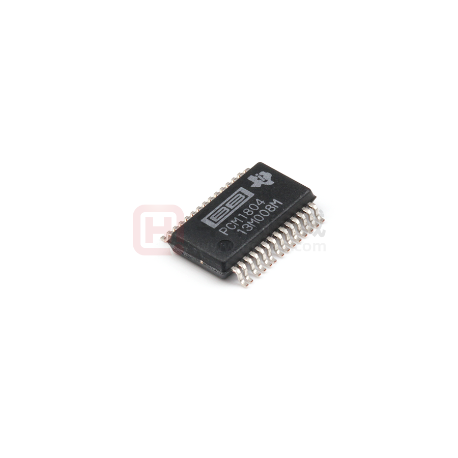
PCM1804
SLES022A – DECEMBER 2001
FULL DIFFERENTIAL ANALOG INPUT 24-BIT, 192-kHz STEREO A/D CONVERTER
FEATURES D 24-Bit Delta-Sigma Stereo A/D Converter D High Performance:
– Dynamic Range: 112 dB (Typically) – SNR: 111 dB (Typically) – THD+N: -102 dB (Typically) High Performance Linear Phase antialias Digital Filter: – Pass-Band Ripple: ±0.005 dB – Stop-Band Attenuation: –100 dB Fully Differential Analog Input: ±2.5 V Audio Interface: Master or Slave Mode Selectable Data Formats: Left Justified, I2S, Standard 24-Bit and DSD Function: – Peak Detection – Low-Cut Filter (HPF): –3 dB at 1 Hz, fS = 48 kHz Sampling Rate up to 192 kHz System Clock: 128 fS, 256 fS, 384 fS, 512 fS, or 768 fS Dual Power Supplies: – 5 V for Analog – 3.3 V for Digital Power Dissipation: 225 mW
PACKAGE DRAWING NUMBER 28DB
D Small 28-Pin SSOP D DSD Output: 1 Bit, 64 fS D Lead-Free Product APPLICATIONS D AV Amp D MD Player D Digital VTR D Digital Mixer D Digital Recorder DESCRIPTION
The PCM1804 is a high-performance single chip stereo A/D converter with full differential analog voltage input. The PCM1804 uses a precision delta-sigma modulator and includes a linear phase antialias digital filter and HPF (low-cut filter) that removes dc offset of the input signal. The PCM1804 is suitable for a wide variety of mid-to-high grade consumer and professional applications, where excellent performance and 5-V analog supply and 3.3-V digital power supply operation are required. The PCM1804 can achieve both PCM audio and DSD format due to precision delta-sigma modulator. The PCM1804 is fabricated on an advanced CMOS process and is available in small 28-pin SSOP package.
D
D D D D
D D D D
PACKAGE/ORDERING INFORMATION PRODUCT PACKAGE OPERATING TEMPERATURE RANGE –10°C to 70°C 10 PACKAGE MARKING PCM1804DB ORDERING NUMBER PCM1804DB PCM1804DBR TRANSPORT MEDIA Tube Tape and Reel
PCM1804DB
28-Lead 28 Lead SSOP
This device contains circuits to protect its inputs and outputs against damage due to high static voltages or electrostatic fields. These circuits have been qualified to protect this device against electrostatic discharges (ESD) of up to 2 kV according to MIL-STD-883C, Method 3015; however, it is advised that precautions be taken to avoid application of any voltage higher than maximum-rated voltages to these high-impedance circuits. During storage or handling, the device leads should be shorted together or the device should be placed in conductive foam. In a circuit, unused inputs should always be connected to an appropriated logic voltage level, preferably either VCC or ground. Specific guidelines for handling devices of this type are contained in the publication Guidelines for Handling Electrostatic-Discharge-Sensitive (ESDS) Devices and Assemblies available from Texas Instruments. Please be aware that an important notice concerning availability, standard warranty, and use in critical applications of Texas Instruments semiconductor products and disclaimers thereto appears at the end of this data sheet.
PRODUCTION DATA information is current as of publication date. Products conform to specifications per the terms of Texas Instruments standard warranty. Production processing does not necessarily include testing of all parameters.
Copyright 2001, Texas Instruments Incorporated
www.ti.com
1
�PCM1804
SLES022A – DECEMBER 2001
pin assignments
PCM1804 PACKAGE (TOP VIEW)
VREFL AGNDL VCOML VINL+ VINL– FMT0 FMT1 S/M OSR0 OSR1 OSR2 BYPAS DGND VDD
1 2 3 4 5 6 7 8 9 10 11 12 13 14
28 27 26 25 24 23 22 21 20 19 18 17 16 15
VREFR AGNDR VCOMR VINR+ VINR– AGND VCC OVFL OVFR RST SCKI LRCK/DSDBCK BCK/DSDL DATA/DSDR
functional block diagram
OSR0 SCKI CLK Control OSR1 OSR2
VINL+ VINL– VCOML AGNDL VREFL
Delta-Sigma Modulator (L)
Decimation Filter (L)
HPF
S/M FMT0 FMT1
VREFL Serial Output Interface VREFR LRCK/DSDBCK BCK/DSDL DATA/DSDR
VREFR AGNDR VCOMR VINR+ VINR–
Delta-Sigma Modulator (R)
Decimation Filter (R)
HPF
OVFL OVFR BYPAS
Power Supply
RST
VCC AGND
DGND
VDD
2
www.ti.com
�PCM1804
SLES022A – DECEMBER 2001
Terminal Functions
TERMINAL NAME AGND AGNDL AGNDR BCK/DSDL BYPAS DATA/DSDR DGND FMT0 FMT1 LRCK/DSDBCK OSR0 OSR1 OSR2 OVFL OVFR RST SCKI S/M VCC VCOML VCOMR VDD VINL– VINL+ VINR– VINR+ PIN 23 2 27 16 12 15 13 6 7 17 9 10 11 21 20 19 18 8 22 3 26 14 5 4 24 25 I/O – – – I/O I O – I I I/O I I I O O I I I – – – – I I I I Analog ground Analog ground for VREFL Analog ground for VREFR Bit clock input/output in PCM mode. L-channel audio data output in DSD mode. § HPF bypass control. High: HPF disable, Low: HPF enable§ L-channel and R-channel audio data output in PCM mode. R-channel audio data output in DSD mode. (DSD output, when DSD mode) Digital ground Audio data format 0. See Table 5† Audio data format 1. See Table 5† Sampling clock input / output in PCM and DSD mode. § Oversampling ratio 0. See Table 1 and Table 2† Oversampling ratio 1. See Table 1 and Table 2† Oversampling ratio 2. See Table 1 and Table 2† Overflow signal of L-channel in PCM mode. This is available in PCM mode only. Overflow signal of R-channel in PCM mode. This is available in PCM mode only. Reset, power down input, active low† System clock input; 128 fS, 256 fS, 384 fS, 512 fS or 768 fS.‡ Master / slave mode selection. See Table 4.† Analog power supply L-channel analog common mode voltage (2.5 V) R-channel analog common mode voltage (2.5 V) Digital power supply L-channel analog input, negative pin L-channel analog input, positive pin R-channel analog input, negative pin R-channel analog input, positive pin DESCRIPTIONS
VREFL 1 – L-channel voltage reference output, requires capacitors for decoupling to AGND VREFR 28 – R-channel voltage reference output, requires capacitors for decoupling to AGND † Schmitt-trigger input with internal pulldown (51 kΩ typically), 5-V tolerant. ‡ Schmitt-trigger input, 5-V tolerant. § Schmitt-trigger input
www.ti.com
3
�PCM1804
SLES022A – DECEMBER 2001
absolute maximum ratings over operating free-air temperature (unless otherwise noted)†
Supply voltage: VCC . . . . . . . . . . . . . . . . . . . . . . . . . . . . . . . . . . . . . . . . . . . . . . . . . . . . . . . . . . . . . . . . . . . . . . . . . . . 6.5 V VDD . . . . . . . . . . . . . . . . . . . . . . . . . . . . . . . . . . . . . . . . . . . . . . . . . . . . . . . . . . . . . . . . . . . . . . . . . . . . . 4 V Ground voltage differences: AGND, AGNDL, AGNDR, DGND . . . . . . . . . . . . . . . . . . . . . . . . . . . . . . . . . . . . . . ±0.1 V Digital input voltage: FMT0, FMT1, S/M, OSR0, OSR1, OSR2, SCKI, RST . . . . . . . . . . . . . . . . . . . . –0.3 V to 6.5 V BYPAS, DATA/DSDR, BCK/DSDL, LRCK/DSDBCK, OVFL, OVFR . . . . . . . . . . . . . . . . . . . . . . . . . . . . . . . . . . . . . . . . . . . . . . . –0.3 V to (VDD + 0.3 V) Analog input voltage: VREFL, VREFR, VCOML, VCOMR, VINL+, VINR+, VINL–, VINR– . . . –0.3 V to (VCC + 0.3 V) Input current (any pins except supplies) . . . . . . . . . . . . . . . . . . . . . . . . . . . . . . . . . . . . . . . . . . . . . . . . . . . . . . . . ±10 mA Ambient temperature under bias, TA . . . . . . . . . . . . . . . . . . . . . . . . . . . . . . . . . . . . . . . . . . . . . . . . . . . . . –40°C to 125°C Storage temperature, Tstg . . . . . . . . . . . . . . . . . . . . . . . . . . . . . . . . . . . . . . . . . . . . . . . . . . . . . . . . . . . . . . –55°C to 150°C Junction temperature, TJ . . . . . . . . . . . . . . . . . . . . . . . . . . . . . . . . . . . . . . . . . . . . . . . . . . . . . . . . . . . . . . . . . . . . . . . 150°C Lead temperature (soldering) . . . . . . . . . . . . . . . . . . . . . . . . . . . . . . . . . . . . . . . . . . . . . . . . . . . . . . . . . . . . . . . . 260°C, 5 s Package temperature (IR reflow, peak) . . . . . . . . . . . . . . . . . . . . . . . . . . . . . . . . . . . . . . . . . . . . . . . . . . . . . . 260°C, 10 s
† Stresses beyond those listed under “absolute maximum ratings” may cause permanent damage to the device. These are stress ratings only, and functional operation of the device at these or any other conditions beyond those indicated under “recommended operating conditions” is not implied. Exposure to absolute-maximum-rated conditions for extended periods may affect device reliability.
4
www.ti.com
�PCM1804
SLES022A – DECEMBER 2001
electrical characteristics, all specifications at TA = 25°C, VCC = 5 V, VDD = 3.3 V, master mode, single-speed mode, fS = 48 kHz, system clock = 256 fS, 24-bit data (unless otherwise noted)
PCM1804DB PARAMETER Resolution DATA FORMAT Audio data interface format Audio data bit length Audio data format DIGITAL INPUT/OUTPUT Logic family See Notes 1 and 2 VIH VIL IIH High-level High level input voltage Low-level input voltage See Note 3 See Notes 1, 2, and 3 VIN = VDD, VIN = VDD, VIN = VDD, VIN = 0 V, VIN = 0 V, IOH = –1 mA, IOL = 1 mA, See Note 1 See Note 2 See Note 3 See Notes 1 and 2 See Note 3 See Note 4 See Note 5 32 256 fS, Single rate, See Note 5 384 fS, Single rate, See Note 5 512 fS, Single rate, See Note 5 System clock frequency 768 fS, Single rate, See Note 5 256 fS, Dual rate, 384 fS, Dual rate, See Note 6 See Note 6 12.288 18.432 24.576 36.864 24.576 36.864 24.576 36.864 ±3 ±4 HPF bypass ±0.2 %/FSR %/FSR %/FSR MHz 2.4 0.4 192 65 TTL compatible 2 2 5.5 VDD 0.8 100 ±10 ±100 ±10 ±50 µA VDC VDC kHz µA VDC VDC Standard, I2S, left justified 24-bits MSB first, 2s complement, DSD TEST CONDITIONS MIN TYP 24 MAX UNIT Bits
High level input current High-level in ut current
IIL VOH VOL fS
Low-level Low level input current High-level output voltage Low-level output voltage Sampling frequency
CLOCK FREQUENCY
128 fS, Quad rate, See Note 7 192 fS, Quad rate, See Note 7 DC ACCURACY Gain mismatch channel-to-channel Gain error (VIN = –0.5 dB) Bipolar zero error
NOTES: 1. Pins 6–11, 19: FMT0, FMT1, S/M, OSR0, OSR1, OSR2, RST (Schmitt-trigger input with internal pulldown (51 kΩ typically), 5 V tolerant) 2. Pin 18: SCKI (Schmitt-trigger input, 5 V tolerant) 3. Pins 12, 16–17: BYPAS, BCK/DSDL, LRCK/DSDBCK (in slave mode, Schmitt-trigger input) 4. Pins 15–17, 20, and 21: DATA/DSDR, BCK/DSDL, LRCK/DSDBCK (in master mode), OVFR, OVFL 5. Single rate, fS = 48 kHz 6. Dual rate, fS = 96 kHz 7. Quad rate, fS = 192 kHz
www.ti.com
5
�PCM1804
SLES022A – DECEMBER 2001
electrical characteristics, all specifications at TA = 25°C, VCC = 5 V, VDD = 3.3 V, master mode, single-speed mode, fS = 48 kHz, system clock = 256 fS, 24-bit data (unless otherwise noted) (continued)
PCM1804DB PARAMETER DYNAMIC PERFORMANCE (see Note 8) VIN = –0.5 dB VIN = –60 dB THD+N Total harmonic di t ti T t lh i distortion lus noise plus noise VIN = –0.5 dB VIN = –60 dB VIN = –0.5 dB VIN = –60 dB VIN = –0.5 dB VIN = –60 dB 60 dB DSD mode fS = 48 kHz, fS = 96 kHz, fS = 192 kHz, DSD mode fS = 48 kHz, fS = 96 kHz, fS = 192 kHz, ANALOG INPUT Input voltage Center voltage Input impedance DIGITAL FILTER PERFORMANCE Pass-band edge Stop-band edge Pass-band ripple Stop-band attenuation Pass-band edge (–0.005 dB) Pass-band edge (–3 dB) Stop-band edge Pass-band ripple Stop-band attenuation Group delay HPF frequency response –3 dB Single rate, dual rate Single rate, dual rate Single rate, dual rate Single rate, dual rate Quad rate Quad rate Quad rate Quad rate Quad rate –135 37/fS fS/48000 0.77 fS ±0.005 –100 0.375 fS 0.49 fS 0.547 fS ±0.005 0.453 fS Hz Hz dB dB Hz Hz Hz dB dB s Hz Single end Differential input ±2.5 2.5 10 V VDC kΩ System clock = 256 fS System clock = 256 fS System clock = 128 fS System clock = 256 fS System clock = 256 fS System clock = 128 fS 97 105 –102 fS = 48 kHz, System clock = 256 fS kHz fS = 96 kHz, System clock = 256 fS kHz fS = 192 kHz, System clock = 128 fS kHz DSD mode fS = 48 kHz, System clock = 256 fS fS = 96 kHz, System clock = 256 fS fS = 192 kHz, System clock = 128 fS 106 –49 –101 –47 –101 –47 –100 112 112 112 112 111 111 111 111 109 107 107 dB dB dB dB –95 TEST CONDITIONS MIN TYP MAX UNIT
Dynamic range (A weighted) (A-weighted)
SNR (A weighted) (A-weighted)
Channel se aration separation
NOTE 8: fIN = 1 kHz, using Audio Precision’s System II, RMS mode with 20-kHz LPF and 400-Hz HPF in calculation for single rate, with 40-kHz LPF for dual and quad rate in calculation.
6
www.ti.com
�PCM1804
SLES022A – DECEMBER 2001
electrical characteristics, all specifications at TA = 25°C, VCC = 5 V, VDD = 3.3 V, master mode, single-speed mode, fS = 48 kHz, system clock = 256 fS, 24-bit data (unless otherwise noted) (continued)
PCM1804DB PARAMETER POWER SUPPLY REQUIREMENTS VCC VDD ICC IDD Supply current 4.75 Supply voltage range VCC = 5 V, See Notes 5, 6, and 7 VDD = 3.3 V, See Notes 5 and 9 VDD = 3.3 V, See Notes 6 and 9 VDD = 3.3 V, See Notes 7 and 9 Operation, Operation, PD Power dissipation Operation, VCC = 5 V, VDD = 3.3 V, VCC = 5 V, VDD = 3.3 V, VCC = 5 V, VDD = 3.3 V, See Notes 5 and 9 See Notes 6 and 9 See Notes 7 and 9 3 5 3.3 35 15 27 18 225 265 235 5 –10 100 70 °C °C/W mW 290 5.25 3.6 45 20 mA VDC TEST CONDITIONS MIN TYP MAX UNIT
Power down, VCC = 5 V, VDD = 3.3 V TEMPERATURE RANGE Operation temperature θJA Thermal resistance 28-pin SSOP NOTES: 5. Single rate, fS = 48 kHz 6. Dual rate, fS = 96 kHz 7. Quad rate, fS = 192 kHz 9. Minimum load on DATA/DSDR (pin 15)
www.ti.com
7
�PCM1804
SLES022A – DECEMBER 2001
TYPICAL CHARACTERISTICS single rate
TOTAL HARMONIC DISTORTION PLUS NOISE (–0.5 dB, –60 dB) vs TEMPERATURE
–90 –35 120
THD+N – Total Harmonic Distortion Plus Nouse – dB (–0.5 dB)
DYNAMIC RANGE AND SNR vs TEMPERATURE
–95
–40
Dynamic Range and SNR – dB
115 Dynamic Range
–100
–45 –0.5 dB
110
SNR
–105
–60 dB
–50
105
–110 –20
0
20 40 T – Temperature – °C
60
–55 80
100 –20
0
20 40 T – Temperature – °C
60
80
Figure 1
TOTAL HARMONIC DISTORTION PLUS NOISE (–0.5 dB, –60 dB) vs SUPPLY VOLTAGE
–90
Figure 2
THD+N – Total Harmonic Distortion Plus Nouse – dB (–0.5 dB)
–35
–95
–40
–100 –0.5 dB
–45
–105
–60 dB
–50
–110 4.5
4.75 5 5.25 VCC – Supply Voltage – V
–55 5.5
Figure 3
† All specifications at T = 25°C, V A CC = 3.3 V, VDD = 5 V, master mode, fS = 48 kHz, system clock = 256 fS, 24-bit data, unless otherwise noted.
8
www.ti.com
THD+N – Total Harmonic Distortion Plus Nouse – dB (–60 dB)
�PCM1804
SLES022A – DECEMBER 2001
TYPICAL CHARACTERISTICS single rate (continued)
DYNAMIC RANGE AND SNR vs SUPPLY VOLTAGE
120
Dynamic Range and SNR – dB
115 Dynamic Range
110
SNR
105
100 4.5
4.75 5 5.25 VCC – Supply Voltage – V
5.5
Figure 4
TOTAL HARMONIC DISTORTION PLUS NOISE (–0.5 dB, –60 dB) vs SAMPLING FREQUENCY
–90 –35
THD+N – Total Harmonic Distortion Plus Nouse – dB (–0.5 dB)
–95
–40
–100
–0.5 dB
–45
–105
–60 dB
–50
–110
–55 32 44.1 48 fS – Sampling Frequency – kHz
Figure 5
† All specifications at T = 25°C, V A CC = 3.3 V, VDD = 5 V, master mode, fS = 48 kHz, system clock = 256 fS, 24-bit data, unless otherwise noted.
THD+N – Total Harmonic Distortion Plus Nouse – dB (–60 dB)
www.ti.com
9
�PCM1804
SLES022A – DECEMBER 2001
TYPICAL CHARACTERISTICS single rate (continued)
DYNAMIC RANGE AND SNR vs SAMPLING FREQUENCY
120 0 –20 Dynamic Range and SNR – dB –40 Amplitude – dB Dynamic Range –60 –80 –100 –120 –140 100 44.1 32 48 fS – Sampling Frequency – kHz –160 0 12000 f – Frequency – Hz 24000 Output Spectrum: –0.50 dB, N = 8192
AMPLITUDE vs FREQUENCY
115
110
SNR
105
Figure 6
AMPLITUDE vs FREQUENCY
0 –20 –40 Amplitude – dB –60 –80 –100 –120 –140 –160 0 12000 f – Frequency – Hz 24000 Output Spectrum: –60 dB, N = 8192 fS = 96 kHz, System Clock = 256 fS THD+N – Totla Harmonic Distortion Plus Noise – dB 0
Figure 7
TOTAL HARMONIC DISTORTION PLUS NOISE vs SIGNAL LEVEL
–20
–40
–60
–80
–100
–120 –100
–80
–60
–40
–20
0
Signal Level – dB
Figure 8
Figure 9
† All specifications at T = 25°C, V A CC = 3.3 V, VDD = 5 V, master mode, fS = 48 kHz, system clock = 256 fS, 24-bit data, unless otherwise noted.
10
www.ti.com
�PCM1804
SLES022A – DECEMBER 2001
TYPICAL CHARACTERISTICS dual rate
AMPLITUDE vs FREQUENCY
0 –20 –40 Amplitude – dB Amplitude – dB –60 –80 –100 –120 –140 –160 0 24000 f – Frequency – Hz 48000 Output Spectrum: –0.5 dB, N = 8192 fS = 96 kHz, System Clock = 256 fS 0 –20 –40 –60 –80 –100 –120 –140 –160 0 24000 f – Frequency – Hz 48000 Output Spectrum: –60 dB, N = 8192
AMPLITUDE vs FREQUENCY
Figure 10
Figure 11
quad rate
AMPLITUDE vs FREQUENCY
0 –20 –40 Amplitude – dB Output Spectrum: –0.5 dB, N = 8192 Amplitude – dB –60 –80 –100 –120 –140 –160 0 48000 f – Frequency – Hz 96000 fS = 192 kHz, System Clock = 128 fS 0 –20 –40 –60 –80 –100 –120 –140 –160 0 48000 f – Frequency – Hz 96000 Output Spectrum: –60 dB, N = 8192 fS = 192 kHz, System Clock = 128 fS
AMPLITUDE vs FREQUENCY
Figure 12
† All specifications at T = 25°C, V A CC = 3.3 V, VDD = 5 V, master mode, 24-bit data, unless otherwise noted.
Figure 13
www.ti.com
11
�PCM1804
SLES022A – DECEMBER 2001
TYPICAL CHARACTERISTICS DSD mode
AMPLITUDE vs FREQUENCY
0 –20 –40 Amplitude – dB –60 –80 –100 –120 –140 –160 0 Amplitude – dB Output Spectrum: –0.5 dB, N = 8192 0 –20 –40 –60 –80 –100 –120 –140 –160 0 11025 f – Frequency – Hz 22050
AMPLITUDE vs FREQUENCY
Output Spectrum: –60 dB, N = 8192
11025 f – Frequency – Hz
22050
Figure 14
Figure 15
† All specifications at TA = 25°C, VCC = 3.3 V, VDD = 5 V, master mode, fS = 44.1 kHz, system clock = 16.9344 MHz, unless otherwise noted.
linear phase antialias digital filter frequency response
OVERALL CHARACTERISTICS AT SINGLE RATE FILTER
50 fS = 48 kHz 0
STOPBAND ATTENUATION CHARACTERISTICS AT SINGLE RATE FILTER
0 –10 –20 –30 –40 –50 –60 –70 –80 –90 –100 –110 –120 –130 –140 –150 0 0.25 0.5 0.75 1 Normalized Frequency – × fS fS = 48 kHz
Amplitude – dB
–50
–100
–150
–200 0 0.5 1 1.5 2 2.5 3 Normalized Frequency – × fS 3.5 4
Amplitude – dB
Figure 16
Figure 17
12
www.ti.com
�PCM1804
SLES022A – DECEMBER 2001
TYPICAL CHARACTERISTICS linear phase antialias digital filter frequency response (continued)
PASSBAND RIPPLE CHARACTERISTICS AT SINGLE RATE FILTER
0.02 fS = 48 kHz 0 0
TRANSIENT BAND CHARACTERISTICS AT SINGLE RATE FILTER
fS = 48 kHz –1 –2 –3 Amplitude – dB –4 –5 –6 –7 –8 –9
Amplitude – dB
–0.02
–0.04
–0.06
–0.08
–0.1 0 0.1 0.2 0.3 0.4 0.5 Normalized Frequency – × fS 0.6
–10 0.45
0.47 0.49 0.51 0.53 Normalized Frequency – × fS
0.55
Figure 18
OVERALL CHARACTERISTICS AT DUAL RATE FILTER
50 fS = 96 kHz 0
Figure 19
STOPBAND ATTENUATION CHARACTERISTICS AT DUAL RATE FILTER
0 –10 –20 –30 –40 –50 –60 –70 –80 –90 –100 –110 –120 –130 –140 –150 0 0.25 0.5 0.75 Normalized Frequency – × fS 1 fS = 96 kHz
Amplitude – dB
–50
–100
–150
–200 0 0.2 0.4 0.6 0.8 1 1.2 1.4 1.6 1.8 2 Normalized Frequency – × fS
Figure 20
Amplitude – dB
Figure 21
www.ti.com
13
�PCM1804
SLES022A – DECEMBER 2001
TYPICAL CHARACTERISTICS linear phase antialias digital filter frequency response (continued)
PASSBAND RIPPLE CHARACTERISTICS AT DUAL RATE FILTER
0.02 fS = 96 kHz –1 0 –2 –3 Amplitude – dB –4 –5 –6 –7 –8 –9 –0.1 0 0.1 0.2 0.3 0.4 0.5 Normalized Frequency – × fS 0.6 –10 0.45 0.47 0.49 0.51 0.53 0.55 0 fS = 96 kHz
TRANSIENT BAND CHARACTERISTICS AT DUAL RATE FILTER
Amplitude – dB
–0.02
–0.04
–0.06
–0.08
Normalized Frequency – × fS
Figure 22
Figure 23
OVERALL CHARACTERISTICS AT QUAD RATE FILTER
50 fS = 192 kHz 0
STOPBAND ATTENUATION CHARACTERISTICS AT QUAD RATE FILTER
0 –10 –20 –30 –40 –50 –60 –70 –80 –90 –100 –110 –120 –130 –140 –150 0 0.25 0.5 0.75 Normalized Frequency – × fS 1 fS = 192 kHz
Amplitude – dB
–50
–100
–150
–200 0 0.1 0.2 0.3 0.4 0.5 0.6 0.7 0.8 0.9 1 Normalized Frequency – × fS
Figure 24
Amplitude – dB
Figure 25
14
www.ti.com
�PCM1804
SLES022A – DECEMBER 2001
TYPICAL CHARACTERISTICS linear phase antialias digital filter frequency response (continued)
PASSBAND RIPPLE CHARACTERISTICS AT QUAD RATE FILTER
0.02 fS = 192 kHz –1 0 –2 –3 Amplitude – dB –4 –5 –6 –7 –8 –9 –0.1 0 0.1 0.2 0.3 0.4 0.5 Normalized Frequency – × fS 0.6 –10 0.45 0.47 0.49 0.51 0.53 Normalized Frequency – × fS 0.55 –3.90 dB at 0.5 fS 0 fS = 192 kHz
TRANSIENT BAND CHARACTERISTICS AT QUAD RATE FILTER
Amplitude – dB
–0.02
–0.04
–0.06
–0.08
Figure 26
Figure 27
HPF (low-cut filter) frequency response
STOPBAND CHARACTERISTICS
0 0.2
PASSBAND CHARACTERISTICS
–20
0
Amplitude – dB
–40
Amplitude – dB 0 0.1 0.2 0.3 Normalized Frequency – × fS/1000 0.4
–0.2
–0.4
–60
–0.6
–80 –0.8
–100
–1 0 0.5 1 1.5 2 2.5 3 3.5 4 Normalized Frequency – × fS/1000
Figure 28
Figure 29
www.ti.com
15
�PCM1804
SLES022A – DECEMBER 2001
PRINCIPLES OF OPERATION
theory of operation The PCM1804 consists of a band-gap reference, a delta-sigma modulator with full differential architecture for L-channel and R-channel respectively, a decimation filter with a low-cut filter, and a serial interface circuit. Figure 1 illustrates the total architecture of the PCM1804. An on-chip high-precision reference with 10-µF external capacitor(s) provides all the reference voltage needed in the PCM1804, and it defines the full-scale voltage range of both channels. Full differential architecture provides a wide dynamic range and excellent power supply rejection performance. The input signal is sampled at ×128, ×64, and ×32 oversampling rate for oversampling ratio. The single rate, dual rate, and quad rate eliminate the external sample-hold amp. Figure 31 illustrates how the PCM1804 for each oversampling ratio decimates the modulator output down to PCM data when the modulator is running at 6.144 MHz. The delta-sigma modulation randomizes the modulator outputs and reduces the idle tone level. The oversampled data stream from the delta-sigma modulator is converted to a 1 fS, 24-bit digital signal, while removing high-frequency noise components by a decimation filter. The dc components of the signal are removed by the HPF, and the HPF output is converted to a time-multiplexed serial signal through the serial interface, which provides flexible serial formats and master/slave modes. The PCM1804 also has a DSD output mode. The PCM1804 can output directly the signal from the modulators to the DSDL (pin 16) and the DSDR (pin 15).
OSR0 SCKI CLK Control OSR1 OSR2
VINL+ VINL– VCOML AGNDL VREFL
Delta-Sigma Modulator (L)
Decimation Filter (L)
HPF
S/M FMT0 FMT1
VREFL Serial Output Interface VREFR LRCK/DSDBCK BCK/DSDL DATA/DSDR
VREFR AGNDR VCOMR VINR+ VINR–
Delta-Sigma Modulator (R)
Decimation Filter (R)
HPF
OVFL OVFR BYPAS
Power Supply
RST
VCC AGND
DGND
VDD
Figure 30. Total Block Diagram of PCM1804
16
www.ti.com
�PCM1804
SLES022A – DECEMBER 2001
PRINCIPLES OF OPERATION
theory of operation (continued)
0
Quad-Rate Filter
–20 –40 Level – dB –60 –80 –100 –120 –140 –160 0
Single Rate Filter Dual-Rate Filter Modulator
48
96 144 f – Frequency – kHz
192
Figure 31. Spectrum of Modulator Output and Decimation Filter system clock input The PCM1804 supports 128 fS, 192 fS (only master mode at quad rate), 256 fS, 384 fS, 512 fS, and 768 fS as a system clock, where fS is the audio sampling frequency. The system clock must be supplied on SCKI (pin 18). Table 1 shows the relationship of typical sampling frequency and the system clock frequency, and Figure 32 shows system clock timing. In master mode, the system clock rate is selected by OSR2 (pin 11), OSR1 (pin 10), and OSR0 (pin 9) as shown in Table 1. In slave mode, the system clock rate is automatically detected. In DSD mode, OSR2 (pin 11), OSR1 (pin 10), OSR0 (pin 9), and the system clock frequency are fixed as shown in Table 1 and 3.
tw(SCKH) SCKI tw(SCKL) SCKI 2V 0.8 V PARAMETER System clock pulse width high, tw(SCKH) System clock pulse width low, tw(SCKL) MIN 11 11 UNIT ns ns
Figure 32. System Clock Input Timing
www.ti.com
17
�PCM1804
SLES022A – DECEMBER 2001
PRINCIPLES OF OPERATION
power-on and reset functions The PCM1804 has both an internal power-on reset circuit and an RST (pin 19). For internal power-on reset, initialize (reset) is done automatically at the timing the power supply VDD exceeds 2 V (typ) and VCC exceeds 4 V (typ). RST accepts external forced reset, and a low level on RST initiates the reset sequence. As the internal pull-down resistor terminates RST, no connection of RST is equal to the low-level input. As the system clock is used as a clock signal of the reset circuit, the system clock has to be supplied as soon as power is supplied; more specifically, at least three system clocks are required prior to VDD > 2 V, VCC > 4 V and RST = high. During either VDD < 2 V (typ), VCC < 4 V (typ), or RST = low, and 1/fS (max) count after VDD > 2 V (typ), VCC > 4 V (typ) and RST = high, the PCM1804 stays in the reset state and the digital output is forced to zero. The digital output is valid after the reset state is released and the time of 1116/fS is passed. Figure 33 and Figure 34 illustrate the internal power on reset and external reset timing. Figure 35 illustrates the digital output for power on reset and control. The PCM1804 needs RST = low when SCKI, LRCK, BCK (in slave mode), and control pins are changed. power-down function The PCM1804 has a power-down feature that is controlled by the RST (pin 19). Entering the power-down mode is done by keeping the RST low-level input for over 65536/fS. In the master mode, the SCKI (pin 18) is used as the clock signal of the power-down counter. While in the slave mode, the SCKI (pin 18) and the LRCK (pin 17) are used as the clock signal. The clock(s) has to be supplied until the power-down sequence completes. As soon as RST goes high, the PCM1804 starts the reset-release sequence described in the power-on and reset functions section. oversampling ratio Oversampling ratio is selected by OSR2 (pin 11), OSR1 (pin 10) and OSR0 (pin 9) as shown in Table 1 and Table 2. The PCM1804 needs RST = low when OSR2, OSR1, and OSR0 pins are changed. Table 1. Oversampling Ratio in Master Mode
OSR2 Low Low Low Low High High High High High OSR1 Low Low High High Low Low High High Low OSR0 Low High Low High Low High Low High Low OVERSAMPLING RATIO Single rate (× 128 fS) Single rate (× 128 fS) Single rate (× 128 fS) Single rate (× 128 fS) Dual rate (× 64 fS) Dual rate (× 64 fS) Quad rate (× 32 fS) Quad rate (× 32 fS) DSD mode (× 64 fS) DSD mode (× 64 fS) SYSTEM CLOCK RATE 768 fS 512 fS 384 fS 256 fS 384 fS 256 fS 192 fS{ 128 fS 384 fS 256 fS
High Low High † Only master mode at quad rate
18
www.ti.com
�PCM1804
SLES022A – DECEMBER 2001
PRINCIPLES OF OPERATION
Table 2. Oversampling Ratio in Slave Mode
OSR2 Low Low Low Low High High High High OSR1 Low Low High High Low Low High High OSR0 Low High Low High Low High Low High OVERSAMPLING RATIO Single rate (× 128 fS) Dual rate (× 64 fS) Quad rate (× 32 fS) Reserved Reserved Reserved Reserved Reserved SYSTEM CLOCK RATE Automatically detected Automatically detected Automatically detected – – – – –
Table 3. Sampling Frequency and System Clock Frequency
OVERSAMPLING RATIO SAMPLING FREQUENCY 32 kHz Single rate (see Note 10) rate (see Note 10) 44.1 kHz 48 kHz Dual rate (see Note 11) Quad rate (see Note 12) 88.2 kHz 96 kHz 176.4 kHz 192 kHz 128 fS — — — — — 22.5792 24.576 SYSTEM CLOCK FREQUENCY (MHz) 192 fS{ 256 fS 384 fS 512 fS — — — — — 33.8688 36.864 — 8.192 11.2896 12.288 22.5792 24.576 12.288 16.9344 18.432 33.8688 36.864 — — 16.384 22.5792 24.576 — — — — 768 fS 24.576 33.8688 36.864 — — — —
DSD mode (see Note 11) 44.1 kHz † Only master mode NOTES: 10. Modulator is running at 128 fS 11. Modulator is running at 64 fS 12. Modulator is running at 32 fS
16.9344 for 384 fS, 11.2896 for 256 fS
VCC / VDD
4.4 V / 2.2 V 4V/2V 3.6 V / 1.8 V
Reset Internal Reset
Reset Removal
1024 System Clock + 1/fS(max)
System Clock
Figure 33. Internal Power-On Reset Timing
www.ti.com
19
�PCM1804
SLES022A – DECEMBER 2001
PRINCIPLES OF OPERATION
RST tRST RST Pulse Width (tRST) = 40 ns (min) Reset Internal Reset 1/fS (max) System Clock Reset Removal
Figure 34. External Reset Timing
Power ON RST ON
Reset Removal
Internal Reset
RESET
READY / OPERATION
1116 / fS Data (A) NOTES: A. In case of DSD mode, DSDL is also controlled like DSDR. B. The HPF transient response appears initially. Zero Data Converted Data (B)
Figure 35. ADC Digital Output for Power-On Reset and RST Control audio data interface The PCM1804 interfaces the audio system through BCK/DSDL (pin 16), LRCK/DSDBCK (pin 17), and DATA/DSDR (pin 15). The PCM1804 needs RST = low when in the interface mode and/or the data format are changed. interface mode The PCM1804 supports master mode and slave mode as interface modes, which are selected by S/M (pin 8) as shown in Table 4. In master mode, the PCM1804 provides the timing of the serial audio data communications between the PCM1804 and the digital audio processor or external circuit. While in slave mode, the PCM1804 receives the timing of data transfer from an external controller. Slave mode is not available for DSD. Table 4. Interface Mode
S/M Low High MODE Master mode Slave mode
20
www.ti.com
�PCM1804
SLES022A – DECEMBER 2001
PRINCIPLES OF OPERATION
data format The PCM1804 supports four audio data formats in both of master and slave mode, and these data formats are selected by the FMT0 (pin 6) and FMT1 (pin 7) as shown in Table 5. Table 5. Data Format
FMT1 Low Low High High FMT0 Low High Low High FORMAT PCM, Left justified, 24 bit. PCM, I2S, 24 bit. PCM, Standard, 24 bit DSD MASTER Yes Yes Yes Yes SLAVE Yes Yes Yes —
interface timing for PCM Figure 36 through Figure 38 illustrate the interface timing for PCM. (1) Left-Justified Data Format; L-Channel = High, R-Channel = Low
1/fS LRCK BCK DATA 123 22 23 24 123 22 23 24 12 L-Channel R-Channel
(2) I2S Data Format; L-Channel = Low, R-Channel = High
1/fS LRCK BCK DATA 123 22 23 24 123 22 23 24 12 L-Channel R-Channel
(3) Standard Data Format; L-Channel = High, R-Channel = Low
1/fS LRCK BCK DATA 22 23 24 123 22 23 24 123 22 23 24 L-Channel R-Channel
NOTE: LRCK and BCK work as outputs at master mode, inputs at slave mode, respectively.
Figure 36. Audio Data Format for PCM
www.ti.com
21
�PCM1804
SLES022A – DECEMBER 2001
PRINCIPLES OF OPERATION
interface timing for PCM (continued)
t(LRCP) LRCK tw(BCKH) tw(BCKL) t(CKLR) 0.5 VDD t(BCKP) DATA t(CKDO) t(LRDO) 0.5 VDD 0.5 VDD
BCK
PARAMETERS BCK period, t(BCKP) BCK pulse width high, tw(BCKH) BCK pulse width low, tw(BCKL) Delay time BCK falling edge to LRCK valid, t(CKLR) LRCK period, t(LRCP) Delay time BCK falling edge to DATA valid, t(CKDO) Delay time LRCK edge to DATA valid, t(LRDO) Rising time of all signals, tr Falling time of all signals, tf NOTES: A. Rising and falling time is measured from 10% to 90% of IN/OUT signals swing. B. Load capacitance of all signals are 10 pF. C. t(BCKP) is fixed at 1/(64 fS) in case of master mode.
MIN 32 32 –5
TYP 1/(64 fS)
MAX
UNIT ns ns
15 1/fS 15 15 10 10
ns ns ns ns ns
–5 –5
Figure 37. Audio Data Interface Timing for PCM (Master Mode: LRCK and BCK Work as Outputs)
22
www.ti.com
�PCM1804
SLES022A – DECEMBER 2001
PRINCIPLES OF OPERATION
interface timing for PCM (continued)
t(LRCP) LRCK tw(BCKH) BCK t(BCKP) DATA t(CKDO) t(LRDO) 0.5 VDD tw(BCKL) t(LRHD) t(LRSU) 1.4 V
1.4 V
PARAMETERS BCK period, t(BCKP) BCK pulse width high, tw(BCKH) BCK pulse width low, tw(BCKL) LRCK setup time to BCK rising edge, t(LRSU) LRCK hold time to BCK rising edge, t(LRHD) LRCK period, t(LRCP) Delay time BCK falling edge to DATA valid, t(CKDO) Delay time LRCK edge to DATA valid, t(LRDO) Rising time of all signals, tr Falling time of all signals, tf NOTES: A. Rising and falling time is measured from 10% to 90% of IN/OUT signals swing. B. Load capacitance of DATA/DSDR signal is 10 pF.
MIN 1/(64 fS) 32 32 12 12
TYP 1/(64 fS)
MAX 1/(48 fS)
UNIT ns ns ns ns
1/fS 5 5 25 25 10 10 ns ns ns ns
Figure 38. Audio Data Interface Timing for PCM (Slave Mode: LRCK and BCK Work as Inputs) interface timing for DSD Figure 39 and Figure 40 illustrate the interface timing for DSD.
DSDBCK DSDL Dn–3 Dn–2 Dn–1 Dn Dn+1 Dn+2 Dn+3
DSDR
Dn–3
Dn–2
Dn–1
Dn
Dn+1
Dn+2
Dn+3
Figure 39. Audio Data Format
www.ti.com
23
�PCM1804
SLES022A – DECEMBER 2001
PRINCIPLES OF OPERATION
interface timing for DSD (continued)
tw(BCKH) tw(BCKL) t(CKDO)
DSDBCK t(BCKP)
0.5 VDD
DSDL DSDR
0.5 VDD
PARAMETERS DSDBCK period, t(BCKP) DSDBCK pulse width high, tw(BCKH) DSDBCK pulse width low, tw(BCKL) Delay time DSDBCK falling edge to DSDL, DSDR valid, t(CKDO) Rising time of all signals, tr Falling time of all signals, tf NOTES: A. Rising and falling time is measured from 10% to 90% of IN/OUT signals swing. B. Load capacitance of DSDBCK/DSDL/DSDR signal is 10 pF.
MIN
TYP 354.308 177.154 177.154
MAX
UNIT ns ns ns
–5
15 10 10
ns ns ns
Figure 40. Audio Data Interface Timing for DSD (Mast Mode Only) synchronization with digital audio system for PCM In slave mode, the PCM1804 operates under LRCK synchronized with the system clock SCKI. The PCM1804 does not need specific phase relationship between LRCK and SCKI, but does require the synchronization of LRCK and SCKI. If the relationship between LRCK and SCKI changes more than ±6 BCK during one sample period due to LRCK or SCKI jitter, internal operation of the ADC halts within 1/fS and digital output is forced into BPZ code until resynchronization between LRCK and SCKI is completed. In case of changes less than ±5 BCK, resynchronization does not occur and above digital output control and discontinuity does not occur. Figure 41 illustrates ADC digital output for loss of synchronization and resynchronization. During undefined data, it may generate some noise in the audio signal. Also, the transitions of normal to undefined data and undefined or zero data to normal make a discontinuity of data on the digital output. This may generate noise in the audio signal. In master mode, synchronization loss never occurs. HPF (low-cut filter) bypass control for PCM The built-in function for dc component rejection can be bypassed by BYPAS (pin 12) control. In bypass mode, the dc component of the input analog signal and the internal dc offset are also converted and output in the digital output data. Table 6. HPF Bypass Control
BYPASS Low High LPF (HIGH-PASS FILTER) MODE Normal (dc cut) mode Bypass (through) mode
24
www.ti.com
�PCM1804
SLES022A – DECEMBER 2001
PRINCIPLES OF OPERATION
overflow flag for PCM The PCM1804 has two overflow flag pins, OVFR (pin 20) and OVFL (pin 21). The pins go to high as soon as the analog input goes across the full-scale range. The high level is held for 1.016 s at maximum, and returns to low if the analog input does not go across the full-scale range for the period.
Synchronization Lost State of Synchronization Resynchronization
SYNCHRONOUS
ASYNCHRONOUS
SYNCHRONOUS
1 / fS Data (A) Normal Data Undefined Data
90 / fS Zero Data Converted Data (B)
NOTES: A. Applies only for slave mode, the loss of synchronization never occurs in master mode. B. The HPF transient response appears initially.
Figure 41. ADC Digital Output for Lost of Synchronization and Resynchronization
www.ti.com
25
�PCM1804
SLES022A – DECEMBER 2001
PRINCIPLES OF OPERATION
typical circuit connection diagram Figure 42 illustrates a typical circuit connection diagram in the PCM data format operation.
PCM1804 C1 +1 2 C3 +3 4 + L-Channel In – 6 FMT0 Format [1:0] 7 FMT1 8 Master/Slave 9 Control Oversampling Ratio [2:0] 10 11 12 13 3.3 V C5 + 14 OSR0 OSR1 OSR2 BYPAS DGND VDD OVFR 19 RST 18 SCKI 17 LRCK/DSDBCK 16 BCK/DSDL 15 DATA/DSDR Data Out Data Clock L/R Clock Audio Data Processor Reset System Clock S/M OVFL 20 Overflow VCC 21 AGND 5 C2 28 + VREFL AGNDL VCOML VINL+ VINL– VREFR 27 AGNDR C4 26 + VCOMR VINR+ VINR– 23 C6 22 5V + 25 + 24 – R-Channel In
HPF Bypass
NOTES: A. C1, C2, C5, and C6: Bypass capacitor 0.1-µF ceramic and 10-µF tantalum, depends on layout and power supply. B. C3, C4: Bypass capacitor 0.1-µF tantalum, depends on layout and power supply.
Figure 42. Typical Circuit Connection Diagram at PCM
26
www.ti.com
�PCM1804
SLES022A – DECEMBER 2001
PRINCIPLES OF OPERATION
typical circuit connection diagram (continued) Figure 43 illustrates a typical circuit connection diagram in the DSD data format operation.
PCM1804 C1 +1 2 C3 +3 4 + L-Channel In – 6 FMT0 Format [1:0] 7 FMT1 8 Master/Slave 9 Control Oversampling Ratio [2:0] 10 11 12 13 3.3 V C5 + 14 OSR0 OSR1 OSR2 BYPAS DGND VDD OVFR 19 RST 18 SCKI 17 LRCK/DSDBCK 16 BCK/DSDL 15 DATA/DSDR R-Channel Data Out L-Channel Data Out Data Clock Audio Data Processor Reset System Clock S/M OVFL 20 Overflow VCC 21 AGND 5 C2 28 + VREFL AGNDL VCOML VINL+ VINL– VREFR 27 AGNDR C4 26 + VCOMR VINR+ VINR– 23 C6 22 5V + 25 + 24 – R-Channel In
HPF Bypass
NOTES: A. C1, C2, C5, and C6: Bypass capacitor 0.1-µF ceramic and 10-µF tantalum, depends on layout and power supply. B. C3, C4: Bypass capacitor 0.1-µF tantalum, depends on layout and power supply.
Figure 43. Typical Circuit Connection Diagram at DSD
www.ti.com
27
�PCM1804
SLES022A – DECEMBER 2001
APPLICATION INFORMATION board design and layout considerations
VCC, VDD pins The digital and analog power supply lines to the PCM1804 should be bypassed to the corresponding ground pins with 0.1-µF ceramic and 10-µF tantalum capacitors placed as close to the pins as possible to maximize the dynamic performance of the ADC. Although the PCM1804 has two power lines to maximize the potential of dynamic performance, using one common power supply is recommended to avoid unexpected power supply trouble like latch-up or power-supply sequence. VIN pins Use 100-pF ceramic capacitors between VINL+, VINL–, VINR+, VINR–, and AGND, and 0.022-µF ceramic capacitors between VINL+ and VINL–, VINR+, and VINR– to remove higher-frequency noise at the delta-sigma input section. VREFX, VCOMX inputs Use 0.1-µF ceramic and 10-µF tantalum capacitors between VREFL, VREFR, and corresponding AGNDx, to insure low-source impedance at ADC references. Use 0.1-µF tantalum capacitors between VCOML, VCOMR and corresponding AGNDx to insure low-source impedance of common voltage. These capacitors should be located as close as possible to the VREFL, VREFR, VCOML, and VCOMR pins to reduce dynamic errors on references and common voltage. The dc voltage level of these pins is 2.5 V. DATA/DSDR, BCK/DSDL, and LRCK/DSDBCK pins The DATA/DSDR, BCK/DSDL, and LRCK/DSDBCK pins in master mode have large load drive capability. Locating the buffer near the PCM1804 and minimizing the load capacitance, minimizes the digital analog crosstalk and maximizes the dynamic performance of the ADC. system clock The quality of the system clock may influence dynamic performance, as the PCM1804 operates based on system clock. In that case, it may be required to consider the system clock duty, jitter, and the time difference between system clock transition and BCK/DSDL or LRCK/DSDBCK transition in slave mode. reset control If capacitors larger than 10 µF are used on VREFL and VREFR, the external reset control with a delay time corresponding to the VREFL and VREFR response is required. Also, it works as a power-down control.
application circuit for single-end input
An application circuit for a single-end input circuit is shown in Figure 44. The maximum signal input voltage and differential gain of this circuit is designed as Vinmax = 8.28 Vpp, A = 0.3. Differential gain (Ad) is given by R3/R1(R4/R2) as normal inverted gain amp. Resistor R5 (R6) in the feedback loop gives low-impedance drive operation and noise filtering for analog input of the PCM1804. The circuit technique R5 (R6) is recommended.
28
www.ti.com
�PCM1804
SLES022A – DECEMBER 2001
APPLICATION INFORMATION
R3 = 909 Ω 4.99 kΩ 4.99 kΩ Analog In _ + OPA2134 1/2 10 µ R1 = 3 kΩ + + 100 pF OPA2134 1/2 VCOM 0.1 µF R4 = 909 Ω 100 pF (See Note) 10 µ R2 = 3 kΩ + + 100 pF OPA2134 1/2 NOTE: 3300 pF is recommended if the input signal level is more than –6 dB of FS at 100 kHz is applied in DSD mode. 0.022 µF 100 pF (See Note) PCM1804 _ R5 = 51.1 Ω VIN–
_
R6 = 51.1 Ω VIN+
Figure 44. Application Circuit for Single-Ended Input Circuit (PCM)
VIN+ VIN– _ BGR +
∆Σ Modulator
VCOM
VREF
_ +
Figure 45. Equivalent Circuit of Internal Reference (VCOM, VREF)
www.ti.com
29
�MECHANICAL DATA
MSSO002D – JANUARY 1995 – REVISED SEPTEMBER 2000
MECHANICAL DATA
DB (R-PDSO-G**)
28 PINS SHOWN 0,65 28 0,38 0,22 15 0,15 M
PLASTIC SMALL-OUTLINE
0,15 NOM 5,60 5,00 8,20 7,40
Gage Plane 1 A 14 0°– 8° 0,25 0,95 0,55
Seating Plane 2,00 MAX 0,05 MIN 0,10
PINS ** DIM A MAX
14
16
20
24
28
30
38
6,50
6,50
7,50
8,50
10,50
10,50
12,90
A MIN
5,90
5,90
6,90
7,90
9,90
9,90
12,30 4040065 /D 09/00
NOTES: A. B. C. D.
All linear dimensions are in millimeters. This drawing is subject to change without notice. Body dimensions do not include mold flash or protrusion not to exceed 0,15 mm. Falls within JEDEC MO-150
30
www.ti.com
�IMPORTANT NOTICE Texas Instruments Incorporated and its subsidiaries (TI) reserve the right to make corrections, modifications, enhancements, improvements, and other changes to its products and services at any time and to discontinue any product or service without notice. Customers should obtain the latest relevant information before placing orders and should verify that such information is current and complete. All products are sold subject to TI’s terms and conditions of sale supplied at the time of order acknowledgment. TI warrants performance of its hardware products to the specifications applicable at the time of sale in accordance with TI’s standard warranty. Testing and other quality control techniques are used to the extent TI deems necessary to support this warranty. Except where mandated by government requirements, testing of all parameters of each product is not necessarily performed. TI assumes no liability for applications assistance or customer product design. Customers are responsible for their products and applications using TI components. To minimize the risks associated with customer products and applications, customers should provide adequate design and operating safeguards. TI does not warrant or represent that any license, either express or implied, is granted under any TI patent right, copyright, mask work right, or other TI intellectual property right relating to any combination, machine, or process in which TI products or services are used. Information published by TI regarding third–party products or services does not constitute a license from TI to use such products or services or a warranty or endorsement thereof. Use of such information may require a license from a third party under the patents or other intellectual property of the third party, or a license from TI under the patents or other intellectual property of TI. Reproduction of information in TI data books or data sheets is permissible only if reproduction is without alteration and is accompanied by all associated warranties, conditions, limitations, and notices. Reproduction of this information with alteration is an unfair and deceptive business practice. TI is not responsible or liable for such altered documentation. Resale of TI products or services with statements different from or beyond the parameters stated by TI for that product or service voids all express and any implied warranties for the associated TI product or service and is an unfair and deceptive business practice. TI is not responsible or liable for any such statements.
Mailing Address: Texas Instruments Post Office Box 655303 Dallas, Texas 75265
Copyright 2001, Texas Instruments Incorporated
�


 工商网监
湘ICP备2023018690号
工商网监
湘ICP备2023018690号
