PG
A8
70
PGA870
SBOS436A – DECEMBER 2009 – REVISED FEBRUARY 2011
www.ti.com
High-Speed, Fully Differential, Programmable-Gain Amplifier
Check for Samples: PGA870
FEATURES
DESCRIPTION
•
•
•
•
The PGA870 is a wideband programmable-gain
amplifier (PGA) for high-speed signal chain and data
acquisition systems. The PGA870 has been
optimized to provide high bandwidth, low distortion,
and low noise, making it ideally suited as a 14-bit
analog-to-digital converter (ADC) driver for wireless
base station signal chain applications. The wide gain
range of –11.5 dB to +20 dB can be adjusted in
0.5-dB gain steps through a 6-bit control word applied
to the parallel interface. The gain control interface
may be configured as a level-triggered latch or an
edge-triggered latch, or it may be placed in an
unlatched (transparent) mode. In addition to the 6-bit
gain control, the PGA870 contains a power-down pin
(PD) that can be used to put the device into a
low-current, power-down mode. In this mode, the
quiescent current drops to 2 mA, but the gain control
circuitry remains active, allowing the gain of the
PGA870 to be set before device power-up. The
PGA870 is offered in a QFN-28 PowerPAD™
package.
1
23
•
•
•
•
•
•
•
Wideband +5-V Operation: 650-MHz Bandwidth
Low Impedance, Voltage Mode Output
Wide Gain Range: –11.5 dB to +20 dB
Precise 0.5-dB Gain Steps
Step-to-Step Gain Error = ±0.03 dB
HD2: –93 dBc at 100 MHz
HD3: –88 dBc at 100 MHz
IMD3: –98 dBc at 100 MHz, –95 dBc at 200 MHz
OIP3: +47 dBm at 100 MHz;
Exceeds +45 dBm for Frequencies to 300 MHz
Flexible Gain Control Interface:
– Supports latched and unlatched options
– Gain may be set in power-down state
– Fast setup and hold times: 2.5 ns
Low Disable Current: 2 mA
Pb-Free (RoHS-Compliant) and Green Package
APPLICATIONS
•
•
•
•
RELATED PRODUCTS
Programmable Gain IF Amplifier:
– Differential signal chains
– Single-ended to differential conversion
Fast Gain Control Loops for:
– Test/measurement
– Digital radio signal chains
ADC Driver for Wireless Base Station Signal
Chains: GSM, WCDMA, MC-GSM
Radar/Ranging Systems
DEVICE
DESCRIPTION
THS4509
Wideband, low-noise, low-distortion, fully
differential amplifier
THS7700
High-speed, fully differential 16-bit ADC driver
THS9000
50-MHz to 400-MHz IF/RF Amplifier
ADS6149
14-Bit, 250-MSPS ADC with DDR
LVDS/CMOS Outputs
ADS6145
14-Bit, 125-MSPS ADC with DDR
LVDS/CMOS Outputs
ADS58C48
6b Gain Adjust
Quad channel IF receiver with SNRBoost 3G
Fast Gain Control Loop
+5 V
6b
FS = 250 MHz
6b
Signal Source
Programmable
Attenuator
Bandpass
Filter
PGA870
ADS6149
FPGA
Control Logic
Latch Mode 1
Powerdown 1
Gain Strobe 1
1
2
3
Please be aware that an important notice concerning availability, standard warranty, and use in critical applications of Texas
Instruments semiconductor products and disclaimers thereto appears at the end of this data sheet.
PowerPAD is a trademark of Texas Instruments.
All other trademarks are the property of their respective owners.
PRODUCTION DATA information is current as of publication date.
Products conform to specifications per the terms of the Texas
Instruments standard warranty. Production processing does not
necessarily include testing of all parameters.
© 2009–2011, Texas Instruments Incorporated
�PGA870
SBOS436A – DECEMBER 2009 – REVISED FEBRUARY 2011
www.ti.com
This integrated circuit can be damaged by ESD. Texas Instruments recommends that all integrated circuits be handled with
appropriate precautions. Failure to observe proper handling and installation procedures can cause damage.
ESD damage can range from subtle performance degradation to complete device failure. Precision integrated circuits may be more
susceptible to damage because very small parametric changes could cause the device not to meet its published specifications.
ORDERING INFORMATION (1)
PRODUCT
PACKAGE-LEAD
PACKAGE
DESIGNATOR
PGA870
QFN-28
RHD
(1)
SPECIFIED
TEMPERATURE
RANGE
–40°C to +85°C
PACKAGE
MARKING
ORDERING
NUMBER
TRANSPORT MEDIA,
QUANTITY
PGA870
PGA870IRHDT
Tape and Reel, 250
PGA870
PGA870IRHDR
Tape and Reel, 3000
For the most current package and ordering information see the Package Option Addendum at the end of this document, or see the TI
web site at www.ti.com.
ABSOLUTE MAXIMUM RATINGS (1)
Over operating free-air temperature range, unless otherwise noted.
Power supply
Internal power dissipation
PGA870
UNIT
6
V
See Thermal Characteristics
Input voltage range
VS
V
–65 to +150
°C
Maximum junction temperature (TJ)
+150
°C
Maximum junction temperature (TJ), continuous operation, long-term reliability
+140
°C
Human body model (HBM)
2000
V
Charged device model (CDM)
1000
V
Machine model (MM)
200
V
Storage temperature range
ESD rating
(1)
Stresses above these ratings may cause permanent damage. Exposure to absolute maximum conditions for extended periods may
degrade device reliability. These are stress ratings only, and functional operation of the device at these or any other conditions beyond
those specified is not supported.
DISSIPATION RATINGS (1)
POWER RATING (2)
(TJ= +125°C)
(1)
(2)
PACKAGE
θJP(°C/W)
θJA(°C/W)
TA= +25°C
TA= +85°C
QFN-28
4.1
35
2.9 W
0.87 W
These data were taken with the JEDEC High-K test PCB. For the JEDEC low-K test PCB, θJA is 350°C/W.
Power rating is determined with a junction temperature of +125°C. This is the point where distortion starts to substantially increase and
long-term reliability starts to be reduced. Thermal management of the final printed circuit board should strive to keep the junction
temperature at or below +125° C for best performance and reliability.
2
© 2009–2011, Texas Instruments Incorporated
Product Folder Link(s): PGA870
�PGA870
SBOS436A – DECEMBER 2009 – REVISED FEBRUARY 2011
www.ti.com
ELECTRICAL CHARACTERISTICS: VS+= +5 V
Boldface limits are tested at +25°C.
At TA= +25°C, VS+= +5 V, differential input signal, differential VOUT = 2 VPP, RL= 200 Ω differential, G = 20 dB, and input and
output common-mode at internal midsupply reference, unless otherwise noted.
PGA870IRHD
PARAMETER
CONDITIONS
MIN
TYP
MAX
UNITS
TEST
LEVEL (1)
AC PERFORMANCE
Small-signal bandwidth
G = 20 dB, VO = 100 mVPP
650
MHz
C
Large-signal bandwidth
G = 20 dB, VO = 2 VPP
650
MHz
C
100
MHz
C
Bandwidth for 0.1-dB flatness
Slew rate (differential)
2-V step
2900
V/µs
C
Rise time
2-V step
0.55
ns
C
Fall time
2-V step
0.55
ns
C
Settling time to 1%
2-V step
3
ns
C
Settling time to 0.1%
2-V step
5
ns
C
Noise figure
150-Ω system, Gain = +20 dB, f = 100 MHz
13
dB
C
Gain = +20 dB, f > 1 MHz
30
nV/√Hz
C
Gain = –11 dB, f > 1 MHz
40
nV/√Hz
C
Output-referred voltage noise
HARMONIC DISTORTION
Second-order harmonic distortion
Third-order harmonic distortion
Gain = +20 dB, VO = 2 VPP, RL = 200 Ω
f = 50 MHz
–108
dBc
C
f = 100 MHz
–93
dBc
C
f = 200 MHz
–71
dBc
C
f = 50 MHz
–95
dBc
C
f = 100 MHz
–88
dBc
C
f = 200 MHz
–75
dBc
C
f1(MHz)
Second-order intermodulation
distortion
Third-order intermodulation distortion
Output third-order intercept
2-MHz tone
spacing
2-MHz tone
spacing
VOUT = 2 VPP,
RL = 200 Ω
f2(MHz)
C
49
51
-87
dBc
C
99
101
-90
dBc
C
199
201
-89
dBc
C
49
51
-103
dBc
C
99
101
–98
dBc
C
199
201
–95
dBc
C
49
51
50
dBm
C
99
101
47
dBm
C
199
201
45
dBm
C
30
mV
A
35
mV
B
μV/°C
B
dB
B
DC
Output offset voltage
Average offset voltage drift
TA= +25°C
–30
TA= –40°C to +85°C
–35
TA= –40°C to +85°C
±5
20
INPUT
Input return loss
ZSYS= 150 Ω, frequency < 300MHz
Differential input resistance
-40
129
Differential input capacitance
(1)
B
pF
C
141
Ω
B
76
dB
A
1.2
Single-ended input resistance
Common-mode rejection ratio
Ω
150
TA= +25°C, Gain = 20 dB
54
173
Test levels: (A) 100% tested at +25°C. Over temperature limits set by characterization and simulation. (B) Limits set by characterization
and simulation. (C) Typical value; only for information.
3
© 2009–2011, Texas Instruments Incorporated
Product Folder Link(s): PGA870
�PGA870
SBOS436A – DECEMBER 2009 – REVISED FEBRUARY 2011
www.ti.com
ELECTRICAL CHARACTERISTICS: VS+= +5 V (continued)
Boldface limits are tested at +25°C.
At TA= +25°C, VS+= +5 V, differential input signal, differential VOUT = 2 VPP, RL= 200 Ω differential, G = 20 dB, and input and
output common-mode at internal midsupply reference, unless otherwise noted.
PGA870IRHD
PARAMETER
CONDITIONS
MIN
TYP
TA= +25°C
3.5
3.7
TA= –40°C to +85°C
3.4
UNITS
TEST
LEVEL (1)
V
A
V
B
1.5
V
A
1.6
V
B
VPP
B
VPP
B
mAP
A
mV
A
MAX
OUTPUT
Maximum output voltage high
Minimum output voltage low
Differential output voltage swing
Each output with
100 Ω to
midsupply
TA= +25°C
1.3
TA= –40°C to +85°C
TA= +25°C, RL = 200 Ω
4
4.8
TA= –40°C to +85°C
3.6
Differential output current drive
TA= +25°C, RL = 20 Ω
40
50
Output common-mode offset from
midsupply
TA= +25°C, RL = 20 Ω
–60
±10
Differential output impedance
f = 100 MHz
3.5 / 87
Ω/°
B
Differential output impedance model
Series ROUT,EQ, LOUT,EQ
0.3 / 3.8
Ω / nH
B
60
POWER SUPPLY
Specified operating voltage
Quiescent current
4.75
5
5.25
V
C
TA= +25°C
138
143
148
mA
A
TA= –40°C to +85°C
136
150
mA
B
dB
A
V
A
V
A
4
mA
A
4.8
mA
B
dB
C
TA= +25°C, Gain = 20 dB (2)
54
Device power-up voltage threshold
Ensured on above 2.1 V
2.1
Device power-down voltage threshold
Ensured off below 0.9 V
Power-supply rejection ratio (PSRR)
76
POWER DOWN
Power-down quiescent current
0.9
TA= +25°C
2
TA= –40°C to +85°C
Forward isolation in power-down state
f = 100 MHz
PD pin input bias current
PD= VS–
-110
0.5
PD pin input impedance
20 || 0.5
μA
B
kΩ || pF
C
Turn-on time delay
Measured to output on
16
ns
C
Turn-off time delay
Measured to output off
60
ns
C
GAIN SETTING
–11.5
Gain range
Gain control: G0 to G5
Gain step size
Gain error over entire gain range
–11.5 dB ≤ Gain ≤ +20 dB
+20
A
Bits
B
0.50
dB
A
Absolute gain error
–0.35
±0.05
0.35
dB
A
Step to step gain error
–0.10
±0.03
0.10
dB
A
0.0018
0.0022
0.0026
dB/°C
B
ns
B
V
A
Gain temp coefficient
Gain settling time
DIGITAL INPUTS
dB
6
5
B0 to B5 and Latch
Digital threshold low
0.9
Digital threshold high
2.1
V
A
Current into/out of digital pins
±20
nA
C
Data set up time to GAIN STROBE low
2.5
ns
C
0
ns
C
6.4
ns
C
Data hold time after GAIN STROBE
low
Latency time
(2)
PSRR is defined with respect to a differential output.
4
© 2009–2011, Texas Instruments Incorporated
Product Folder Link(s): PGA870
�PGA870
SBOS436A – DECEMBER 2009 – REVISED FEBRUARY 2011
www.ti.com
PIN CONFIGURATION
VMID1
PD
GND
VS+
GND
GND
GND
28
27
26
25
24
23
22
QFN-28
RHD PACKAGE
(TOP VIEW)
LATCH MODE
1
21
GND
VS+
2
20
VS+
IN+
3
19
OUT+
VMID2
4
18
GND
IN-
5
17
OUT-
VS+
6
16
VS+
GAIN STROBE
7
15
GND
8
9
10
11
12
13
14
(MSB) B5
B4
B3
VS+
B2
B1
B0
PowerPADä
PIN ASSIGNMENTS
PIN NUMBER
1
PIN NAME
LATCH MODE
DESCRIPTION
Controls latched and unlatched acquisition of the gain control word (B0 to B5). See the application section Gain
Control Modes for a detailed description.
2, 6, 11, 16, 20, 25
VS+
+5V power supply
3
IN+
Noninverting input
4
VMID2
Buffer output for the internal midsupply reference. This point is the output of an active buffer which is not intended
to drive an external load. It should be bypassed by a 0.1-μF capacitor.
5
IN–
7
GAIN STROBE
Inverting input
8
B5 (MSB)
Gain control MSB
9
B4
Gain control bit 4
10
B3
Gain control bit 3
12
B2
Gain control bit 2
13
B1
Gain control bit 1
14
B0 (LSB)
Gain control bit 0
17
OUT–
Inverting output
15, 18, 21, 22, 23,
24, 26
GND
Ground
19
OUT+
Noninverting output
27
PD
28
VMID1
Thermal Pad
PowerPAD
Gain latch clock pin
Active low power-down for device analog circuitry. Gain control CMOS circuitry is still active when PD is low.
Chip bypass pin for internal midsupply reference. This point is the midpoint of a resistive voltage divider and is not
intended to function as an input. It should be bypassed with a 0.1-μF capacitor.
Thermal contact for heat dissipation. The thermal pad must be connected to electrical ground.
5
© 2009–2011, Texas Instruments Incorporated
Product Folder Link(s): PGA870
�PGA870
SBOS436A – DECEMBER 2009 – REVISED FEBRUARY 2011
www.ti.com
TYPICAL CHARACTERISTICS
At TA= +25°C, VS+= +5 V, differential input signal, differential VOUT = 2 VPP, RL = 200 Ω differential, G = +20 dB, and input and
output common-mode at internal midsupply reference, unless otherwise noted.
SMALL-SIGNAL AC RESPONSE
Gain Adjusted from –11.5 dB to +5 dB
Gain Adjusted in 0.5-dB Steps
VOUT = 200 mVPP
25
Gain Adjusted in 0.5-dB Steps
VOUT = 200 mVPP
Gain = +5 dB
5
20
0
15
Gain (dB)
Gain (dB)
10
SMALL-SIGNAL AC RESPONSE
Gain Adjusted from +5.5 dB to +20 dB
-5
-10
Gain = +20 dB
10
5
Gain = +5.5 dB
Gain = -11.5 dB
-15
0
10
100
1000
10
1000
Frequency (MHz)
Figure 1.
Figure 2.
LARGE-SIGNAL AC RESPONSE AT FOUR GAINS
DIFFERENTIAL INPUT
LARGE-SIGNAL AC RESPONSE AT FOUR GAINS
SINGLE-ENDED INPUT
30
30
25
25
Gain = 20 dB
20
15
15
Gain = 10 dB
10
5
Gain = 0 dB
0
Gain = -6 dB
-5
Gain = 20 dB
20
Gain (dB)
Gain (dB)
100
Frequency (MHz)
Gain = 10 dB
10
5
Gain = 0 dB
0
Gain = -6 dB
-5
-10
-10
Differential Input
VOUT = 2 VPP
-15
-20
-15
-20
10
100
1000
Single-Ended Input
VOUT = 2 VPP
10
100
1000
Frequency (MHz)
Frequency (MHz)
Figure 3.
Figure 4.
DIFFERENTIAL FREQUENCY RESPONSE vs CAPACITIVE
LOAD
25
CL = 94 pF
20
ROS vs CAPACITIVE LOAD
100
CL = 44 pF
CL =
10 pF
15
ROS (W)
Gain (dB)
CL = 820 pF
CL = 470 pF
10
CL =
16 pF
ROS
CL
PGA870
5
ROS
10
ROS
CL
CL =
20 pF
VOUT
PGA870
CL
ROS
VOUT
CL
0
1
10
100
1000
1
10
100
Frequency (MHz)
Capacitive Load (pF)
Figure 5.
Figure 6.
6
1000
© 2009–2011, Texas Instruments Incorporated
Product Folder Link(s): PGA870
�PGA870
SBOS436A – DECEMBER 2009 – REVISED FEBRUARY 2011
www.ti.com
TYPICAL CHARACTERISTICS (continued)
At TA= +25°C, VS+= +5 V, differential input signal, differential VOUT = 2 VPP, RL = 200 Ω differential, G = +20 dB, and input and
output common-mode at internal midsupply reference, unless otherwise noted.
STEP-TO-STEP GAIN ERROR vs GAIN SETTING
OVER TEMPERATURE
LARGE-SIGNAL GAIN vs GAIN SETTING
25
0.15
20
0.10
Gain Error (dB)
15
Gain (dB)
10
5
0
-40°C
0.05
+25°C
0
-0.05
-0.10
-5
50 MHz
100 MHz
200 MHz
-10
+85°C
-0.15
-0.20
-15
-12-10 -8 -6 -4 -2 0
2
4
6
-12-10 -8 -6 -4 -2 0
8 10 12 14 16 18 20
Figure 7.
8 10 12 14 16 18 20
GAIN STEP RESPONSE: NO LATCH
1.5
Gain Control
3.5
0.02
Gain Code = 111111
1.0
Gain Control (V)
3.0
0
-0.02
-0.04
2.5
0.5
2.0
1.5
0
1.0
-0.5
0.5
0
50 MHz
100 MHz
200 MHz
-1.0
Gain Code = 000000
Amplifier
Output
-0.5
-1.0
-0.08
-12-10 -8 -6 -4 -2 0
2
4
6
-1.5
0
8 10 12 14 16 18 20
100
Gain Setting
200
300
400
500
Time (ns)
Figure 10.
GAIN STEP RESPONSE: LEVEL-TRIGGERED GAIN LATCH
GAIN STEP RESPONSE: EDGE-TRIGGERED LATCH
2.0
Gain Code =
111111
Gain Strobe
1.5
1.0
0.5
0.5
0
-0.5
-1.0
2.5
2.0
Gain Code = 111111
Gain
Strobe
1.5
1.0
Gain Code =
000000
0.5
1.0
0
Time (50 ns/div)
0.5
0
-0.5
-1.0
Amplifier Output (V)
Gain Code =
000000
Amplifier Output (V)
1.0
0
Gain Control, Gain Strobe (V)
Figure 9.
2.5
Amplifier Output (V)
Gain Error (dB)
6
4.0
0.04
Gain Control, Gain Strobe (V)
4
Figure 8.
STEP-TO-STEP GAIN ERROR vs GAIN SETTING
OVER FREQUENCY
-0.06
2
Gain Setting
Gain Setting
Time (50 ns/div)
Figure 11.
Figure 12.
7
© 2009–2011, Texas Instruments Incorporated
Product Folder Link(s): PGA870
�PGA870
SBOS436A – DECEMBER 2009 – REVISED FEBRUARY 2011
www.ti.com
TYPICAL CHARACTERISTICS (continued)
At TA= +25°C, VS+= +5 V, differential input signal, differential VOUT = 2 VPP, RL = 200 Ω differential, G = +20 dB, and input and
output common-mode at internal midsupply reference, unless otherwise noted.
THIRD-ORDER INTERMODULATION DISTORTION
FOR TWO GAINS AND FOUR OUTPUT LOADS (VOUT = 2
VPP)
SECOND-ORDER INTERMODULATION DISTORTION
FOR FOUR OUTPUT LOADS (VOUT = 2 VPP)
-70
VOUT = 2 VPP
DF = 2 MHz
-80
IMD3 (dBc)
IMD2 (dBc)
-75
-85
-90
RL = 100 W
RL = 200 W
RL = 500 W
RL = 1 kW
-95
-100
Gain = +10 dB
50
100
150
200
250
-80
-82
-84
-86
-88
-90
-92
-94
-96
-98
-100
-102
-104
-106
-108
-110
300
VOUT = 2 VPP
DF = 2 MHz
Dashed lines: Gain = -6 dB
Solid lines: Gain = +10 dB
50
100
150
Frequency (MHz)
200
250
300
Frequency (MHz)
Figure 13.
Figure 14.
SECOND-ORDER INTERMODULATION DISTORTION
FOR FOUR OUTPUT LOADS (VOUT = 2 VPP)
THIRD-ORDER INTERMODULATION DISTORTION
FOR TWO GAINS AND FOUR OUTPUT LOADS (VOUT = 2
VPP)
-70
VOUT = 2 VPP
DF = 2 MHz
-75
RL = 100 W
RL = 200 W
RL = 500 W
RL = 1 kW
-80
IMD3 (dBc)
IMD2 (dBc)
RL = 100 W
RL = 200 W
RL = 500 W
RL = 1 kW
-85
-90
-95
-100
Gain = +20 dB
50
100
150
200
250
-80
-82
-84
-86
-88
-90
-92
-94
-96
-98
-100
-102
-104
-106
-108
-110
300
VOUT = 2 VPP
DF = 2 MHz
RL = 100 W
RL = 200 W
RL = 500 W
RL = 1 kW
Dashed lines: Gain = 0 dB
Solid lines: Gain = +20 dB
50
100
150
Frequency (MHz)
200
250
300
Frequency (MHz)
Figure 15.
Figure 16.
OUTPUT THIRD-ORDER INTERCEPT vs FREQUENCY
(VOUT = 2 VPP)
50
VOUT = 2 VPP
RL = 200 W
48
OIP3 (dBm)
46
44
42
40
Gain = +20 dB
Gain = +10 dB
Gain = 0 dB
Gain = -6 dB
38
36
50
100
150
200
250
300
Frequency (MHz)
Figure 17.
8
© 2009–2011, Texas Instruments Incorporated
Product Folder Link(s): PGA870
�PGA870
SBOS436A – DECEMBER 2009 – REVISED FEBRUARY 2011
www.ti.com
TYPICAL CHARACTERISTICS (continued)
At TA= +25°C, VS+= +5 V, differential input signal, differential VOUT = 2 VPP, RL = 200 Ω differential, G = +20 dB, and input and
output common-mode at internal midsupply reference, unless otherwise noted.
THIRD-ORDER INTERMODULATION DISTORTION
FOR TWO GAINS AND FOUR OUTPUT LOADS (VOUT = 3
VPP)
SECOND-ORDER INTERMODULATION DISTORTION
FOR FOUR OUTPUT LOADS (VOUT = 3 VPP)
-70
Gain = +10 dB
-80
IMD3 (dBc)
IMD2 (dBc)
-75
-85
-90
RL = 100 W
RL = 200 W
RL = 500 W
RL = 1 kW
-95
VOUT = 3 VPP
DF = 2 MHz
-100
50
100
150
200
250
-74
-76
-78
-80
-82
-84
-86
-88
-90
-92
-94
-96
-98
-100
300
VOUT = 3 VPP
DF = 2 MHz
Dashed lines: Gain = -6 dB
Solid lines: Gain = +10 dB
50
100
150
Frequency (MHz)
200
250
300
Frequency (MHz)
Figure 18.
Figure 19.
SECOND-ORDER INTERMODULATION DISTORTION
FOR FOUR OUTPUT LOADS (VOUT = 3 VPP)
THIRD-ORDER INTERMODULATION DISTORTION
FOR TWO GAINS AND FOUR OUTPUT LOADS (VOUT = 3
VPP)
-70
VOUT = 3 VPP
DF = 2 MHz
-75
RL = 100 W
RL = 200 W
RL = 500 W
RL = 1 kW
-80
IMD3 (dBc)
IMD2 (dBc)
RL = 100 W
RL = 200 W
RL = 500 W
RL = 1 kW
-85
-90
-95
-100
Gain = +20 dB
50
100
150
200
250
-74
-76
-78
-80
-82
-84
-86
-88
-90
-92
-94
-96
-98
-100
300
VOUT = 3 VPP
DF = 2 MHz
RL = 100 W
RL = 200 W
RL = 500 W
RL = 1 kW
Dashed lines: Gain = 0 dB
Solid lines: Gain = +20 dB
50
100
150
Frequency (MHz)
200
250
300
Frequency (MHz)
Figure 20.
Figure 21.
OUTPUT THIRD-ORDER INTERCEPT vs FREQUENCY
(VOUT = 3 VPP)
52
VOUT = 3 VPP
RL = 200 W
50
OIP3 (dBm)
48
46
44
42
40
Gain = +20 dB
Gain = +10 dB
38
50
100
150
Gain = 0 dB
Gain = -6 dB
200
250
300
Frequency (MHz)
Figure 22.
9
© 2009–2011, Texas Instruments Incorporated
Product Folder Link(s): PGA870
�PGA870
SBOS436A – DECEMBER 2009 – REVISED FEBRUARY 2011
www.ti.com
TYPICAL CHARACTERISTICS (continued)
At TA= +25°C, VS+= +5 V, differential input signal, differential VOUT = 2 VPP, RL = 200 Ω differential, G = +20 dB, and input and
output common-mode at internal midsupply reference, unless otherwise noted.
-65
-50
-55
-70
-60
-75
-65
-80
-70
-85
-75
-90
-80
Dashed lines: 2nd Harmonic
Solid lines: 3rd Harmonic
-95
-100
Gain = -6 dB
Gain = 0 dB
-105
Gain = +10 dB
Gain = +20 dB
-110
0
50
100
150
200
250
-85
-90
-95
-100
300
Second-Order Harmonic Distortion (dBc)
-45
VOUT = 2 VPP
RL = 100 W
-60
-55
-65
-60
-75
-65
-80
-70
-85
-75
-90
Dashed lines: 2nd Harmonic
Solid lines: 3rd Harmonic
-95
-100
Gain = -6 dB
Gain = 0 dB
-105
50
150
200
250
HARMONIC DISTORTION vs FREQUENCY
(VOUT = 2 VPP)
-45
-50
-55
-60
-75
-65
-80
-70
-85
-75
-90
-80
Dashed lines: 2nd Harmonic
Solid lines: 3rd Harmonic
Gain = -6 dB
Gain = +10 dB
Gain = +20 dB
Gain = 0 dB
-105
-110
50
100
150
200
250
-85
-90
-95
-100
300
Second-Order Harmonic Distortion (dBc)
HARMONIC DISTORTION vs FREQUENCY
(VOUT = 2 VPP)
-100
-90
-95
-100
300
Figure 24.
-95
-85
-55
-45
VOUT = 2 VPP
RL = 1 kW
-60
-65
-50
-55
-70
-60
-75
-65
-80
-70
-85
-75
-90
-80
-95
Dashed lines: 2nd Harmonic
Solid lines: 3rd Harmonic
Gain = -6 dB
Gain = +10 dB
Gain = +20 dB
Gain = 0 dB
-100
-105
-110
0
Frequency (MHz)
50
100
150
200
250
-85
-90
-95
Third-Order Harmonic Distortion (dBc)
Second-Order Harmonic Distortion (dBc)
100
-80
Frequency (MHz)
-70
0
Gain = +10 dB
Gain = +20 dB
-110
0
Third-Order Harmonic Distortion (dBc)
-65
-55
Figure 23.
VOUT = 2 VPP
RL = 500 W
-60
-50
-70
Frequency (MHz)
-55
-45
VOUT = 2 VPP
RL = 200 W
-60
Third-Order Harmonic Distortion (dBc)
-55
HARMONIC DISTORTION vs FREQUENCY
(VOUT = 2 VPP)
Third-Order Harmonic Distortion (dBc)
Second-Order Harmonic Distortion (dBc)
HARMONIC DISTORTION vs FREQUENCY
(VOUT = 2 VPP)
-100
300
Frequency (MHz)
Figure 25.
Figure 26.
10
© 2009–2011, Texas Instruments Incorporated
Product Folder Link(s): PGA870
�PGA870
SBOS436A – DECEMBER 2009 – REVISED FEBRUARY 2011
www.ti.com
TYPICAL CHARACTERISTICS (continued)
At TA= +25°C, VS+= +5 V, differential input signal, differential VOUT = 2 VPP, RL = 200 Ω differential, G = +20 dB, and input and
output common-mode at internal midsupply reference, unless otherwise noted.
-65
-45
-50
-70
-55
-75
-60
-80
-65
-85
-70
-90
-75
Dashed lines: 2nd Harmonic
Solid lines: 3rd Harmonic
-95
-100
Gain = -6 dB
Gain = 0 dB
-105
Gain = +10 dB
Gain = +20 dB
-110
0
50
100
150
200
250
-80
-85
-90
-95
300
Second-Order Harmonic Distortion (dBc)
-40
VOUT = 3 VPP
RL = 100 W
-60
-55
-65
-55
-75
-60
-80
-65
-85
-70
-90
Dashed lines: 2nd Harmonic
Solid lines: 3rd Harmonic
-95
-100
Gain = -6 dB
Gain = 0 dB
-105
50
150
200
250
HARMONIC DISTORTION vs FREQUENCY
(VOUT = 3 VPP)
-40
-45
-50
-55
-75
-60
-80
-65
-85
-70
-90
-75
Dashed lines: 2nd Harmonic
Solid lines: 3rd Harmonic
Gain = -6 dB
Gain = 0 dB
-105
Gain = +10 dB
Gain = +20 dB
-110
50
100
150
200
250
-80
-85
-90
-95
300
Second-Order Harmonic Distortion (dBc)
HARMONIC DISTORTION vs FREQUENCY
(VOUT = 3 VPP)
-100
-85
-90
-95
300
Figure 28.
-95
-80
-55
-40
VOUT = 3 VPP
RL = 1 kW
-60
-65
-45
-50
-70
-55
-75
-60
-80
-65
-85
-70
-90
Dashed lines: 2nd Harmonic
Solid lines: 3rd Harmonic
-95
-100
Gain = -6 dB
Gain = 0 dB
-105
Gain = +10 dB
Gain = +20 dB
-110
0
Frequency (MHz)
50
100
150
200
250
-75
-80
-85
-90
Third-Order Harmonic Distortion (dBc)
Second-Order Harmonic Distortion (dBc)
100
-75
Frequency (MHz)
-70
0
Gain = +10 dB
Gain = +20 dB
-110
0
Third-Order Harmonic Distortion (dBc)
-65
-50
Figure 27.
VOUT = 3 VPP
RL = 500 W
-60
-45
-70
Frequency (MHz)
-55
-40
VOUT = 3 VPP
RL = 200 W
-60
Third-Order Harmonic Distortion (dBc)
-55
HARMONIC DISTORTION vs FREQUENCY
(VOUT = 3 VPP)
Third-Order Harmonic Distortion (dBc)
Second-Order Harmonic Distortion (dBc)
HARMONIC DISTORTION vs FREQUENCY
(VOUT = 3 VPP)
-95
300
Frequency (MHz)
Figure 29.
Figure 30.
11
© 2009–2011, Texas Instruments Incorporated
Product Folder Link(s): PGA870
�PGA870
SBOS436A – DECEMBER 2009 – REVISED FEBRUARY 2011
www.ti.com
TYPICAL CHARACTERISTICS (continued)
At TA= +25°C, VS+= +5 V, differential input signal, differential VOUT = 2 VPP, RL = 200 Ω differential, G = +20 dB, and input and
output common-mode at internal midsupply reference, unless otherwise noted.
OUTPUT VOLTAGE NOISE vs FREQUENCY
NOISE FIGURE vs GAIN
45
f = 100 MHz
RSYS = 150 W
40
35
Noise Figure (dB)
Output Voltage Noise (nV/?Hz)
1000
100
30
25
20
15
Gain = +20 dB
Gain = -11.5 dB
10
10
100
1k
10 k
100 k
1M
10 M
10
-12-10 -8 -6 -4 -2 0
100 M
2 4
Figure 32.
DISABLE STEP RESPONSE
LARGE- AND SMALL-SIGNAL
DIFFERENTIAL PULSE RESPONSE
0.9
1.50
0.6
1.25
0.3
1.00
0
0.75
-0.3
0.50
-0.6
0.25
-0.9
-1.2
Amplifier Output
-0.25
Large-Signal Differential Output (V)
1.75
300
400
1.0
0.10
0.5
0.05
0
0
-0.5
-1.0
-0.10
Right Scale
500
-0.15
0
5
10
Time (ns)
15
20
25
Time (2.5 ns/div)
Figure 33.
Figure 34.
FORWARD ISOLATION vs FREQUENCY
IN DISABLED MODE
DIFFERENTIAL INPUT IMPEDANCE
-60
4
Input Impedance Magnitude (W)
160
-80
-100
-120
-140
0
100
200
300
400
500
Magnitude
0
150
-4
140
Phase
130
-8
120
-12
110
-16
100
100 k
Input Impedance Phase (°)
Forward Isolation (dB)
-0.05
Left Scale
-1.5
-1.5
200
0.15
Gain = 20 dB, RL = 200 W
Small-Signal Differential Output (V)
1.2
Amplifier Output (V)
Disable Signal Amplitude (V)
1.5
1.5
Disable Signal
2.00
100
8 10 12 14 16 18 20 22
Figure 31.
2.25
0
6
Gain (dB)
Frequency (Hz)
-20
1M
10 M
100 M
1G
Frequency (Hz)
Frequency (MHz)
Figure 35.
Figure 36.
12
© 2009–2011, Texas Instruments Incorporated
Product Folder Link(s): PGA870
�PGA870
SBOS436A – DECEMBER 2009 – REVISED FEBRUARY 2011
www.ti.com
TYPICAL CHARACTERISTICS (continued)
At TA= +25°C, VS+= +5 V, differential input signal, differential VOUT = 2 VPP, RL = 200 Ω differential, G = +20 dB, and input and
output common-mode at internal midsupply reference, unless otherwise noted.
DIFFERENTIAL INPUT RETURN LOSS
vs FREQUENCY
SINGLE-ENDED INPUT RETURN LOSS
vs FREQUENCY
0
0
ZSYS = 150 W
ZSYS = 150 W
-5
-30
-40
20 dB
10 dB
0 dB
-6 dB
-50
-60
100 M
-10
-15
-20
-25
20 dB
10 dB
0 dB
-6 dB
-30
-35
10 M
1G
100 M
Frequency (Hz)
Frequency (Hz)
Figure 37.
Figure 38.
DIFFERENTIAL OUTPUT IMPEDANCE
DIFFERENTIAL OUTPUT SWING
vs RLOAD
100
100
1G
5.5
90
Phase
80
70
10
60
50
40
1
30
Magnitude
20
Output Impedance Phase (°)
Output Impedance Magnitude (W)
Input Return Loss (dB)
-20
Differential Output Swing (V)
Input Return Loss (dB)
-10
5.0
4.5
4.0
10
0.1
10 k
100 k
1M
0
100 M 300 M
10 M
3.5
100
1k
10 k
Differential Load Resistance, RLOAD (W)
Frequency (Hz)
Figure 39.
Figure 40.
PSRR AND CMRR
vs FREQUENCY
Power-Supply Rejection Ratio (dB)
Common-Mode Rejection Ratio (dB)
90
80
70
PSRR
60
CMRR
50
40
30
20
10
0
1k
10 k
100 k
1M
10 M
100 M
1G
Frequency (Hz)
Figure 41.
13
© 2009–2011, Texas Instruments Incorporated
Product Folder Link(s): PGA870
�PGA870
SBOS436A – DECEMBER 2009 – REVISED FEBRUARY 2011
www.ti.com
APPLICATION INFORMATION
Device Operation
The PGA870 is a wideband, fully differential, programmable-gain amplifier. Looking at the block diagram in
Figure 42, the PGA870 can be separated into the following functional blocks:
•
•
•
•
•
Input Attenuator
Buffered MUX
Output Amplifier
8-bit digital interface
Power function
Attenuator
1
IN-
VS
Gain = +20 dB
2
OUTOutput
Amp
Buffered
MUX
VMID2
OUT+
7
8
IN+
BIAS
Control
Gain Control
PGA870
B0 B1
Gain Latch
Strobe Mode (LSB)
B2
B3
B4
B5
(MSB)
Disable
Figure 42. PGA870 Block Diagram
Input Attenuator
The input stage of the PGA870 consists of a logarithmic R2R ladder and presents a 150-Ω load to the previous
stage. To minimize input return loss and noise figure, it is recommended to provide a 150-Ω matching for that
input. This input can be driven either differentially or single-ended.
This resistive input network is internally biased to midsupply by an internal buffer (VMID2 on pin 4). Proper
bypassing is required on this node (0.1 μF). The buffer midsupply is generated by a passive resistor network
(VMID1 on pin 28). A 0.1-μF capacitor is expected on VMID1 for adequate bypassing. Although VMID1 and VMID2 are
externally accessible, neither of these pins is intended to be externally driven. Additionally, VMID2 is not intended
to drive the midsupply reference to another chip, but can source approximately 200 μA if required.
During power-down operation, the input maintains its nominal differential resistance. However, VMD1 and VMID2
fall to 0 V. The input attenuator is controlled via the three most significant bits (MSBs) of the gain control. Refer
to Table 1 for the step size of each of these three MSBs.
Input Amplifier and Buffered MUX
Following the input attenuator is a programmable buffer stage; the gain of the programmable buffer is controlled
by the three least significant bits (LSBs) of the gain-control word. Refer to Table 1 for the step size of each of
these three LSBs.
Table 1. Gain Bits and Corresponding Gain Step Sizes (in dB)
(MSB)
B5
B4
B3
B2
B1
(LSB)
B0
16
8
4
2
1
0.5
14
© 2009–2011, Texas Instruments Incorporated
Product Folder Link(s): PGA870
�PGA870
SBOS436A – DECEMBER 2009 – REVISED FEBRUARY 2011
www.ti.com
Output Amplifier
The PGA870 has a differential, voltage-mode output stage with a differential output resistance of approximately
0.3 Ω and an inductive reactance equivalent to 3.8 nH. The common-mode output voltage has a nominal value of
VMID2. This output amplifier has a nominal gain of +20 dB.
The nominal load is 200 Ω, but the PGA870 can drive loads as low as 100 Ω with only minor changes to the
device distortion.
The output pins go to a high-impedance state when the device is the power-down state (that is, when PD is low).
8-bit Digital Interface
The 8-bit digital interface is composed of six bits: three MSBs that control the input attenuation and three LSBs
that control the input amplifier and buffered MUX. For more information on this parallel interface, refer to the Gain
Control and Latch Modes section.
Power Function
The PGA870 features a low-power disabled state for the analog circuitry when the power-down (PD) pin is low.
In the disabled state, the digital circuitry remains active, which allows the gain to be set before device power-up.
There is no internal circuitry to provide a nominal bias to this pin. If this pin is to be left open, it must be biased
with an external pull-up resistor.
Note that when the PGA870 is in this low-power mode, the gain can be programmed using the 8-bit digital
interface, the output pins go to a high-impedance state, and the voltage on the midsupply pins biasing the
attenuator (pin 4 and pin 28) goes to 0 V.
Gain Control and Latch Modes
The PGA870 has six bits of gain control (B5 to B0) that give an extended gain range from a maximum gain of 20
dB to a minimum gain of –11.5 dB. The LSB (B0) represents a minimum gain change (step size) of 0.5 dB, and
the LSB (B5) represents a gain change of 16 dB. The equivalent gain step size of each gain control bit is shown
in Table 1. The device voltage gain can be expressed by Equation 1:
GaindB= 20 dB − 0.5 dB × (NG− 63)
(1)
NG is the equivalent base-10 integer number that corresponds to the binary gain control word. A summary of the
63 possible device gains versus NG and the values of B0 to B5 are shown in Table 2.
The high and low voltage thresholds allow all of the gain control pins to be controlled by CMOS circuitry. There
are no internal pull-up resistors on the gain-control pins. If the pins are to be left open, they must be biased with
external pull-up resistors.
The PGA870 can be configured so the device gain is controlled by only the six gain bits (no latch) when the
GAIN STROBE pin and the GAIN MODE pin are both held high. In this operating mode, the device voltage gain
follows the signals on pins B0 to B5. Transients on the six gain bits can cause changes to the PGA870 gain
while in this mode, as well. To combat this possibility, the PGA870 also supports two gain modes where the gain
bit data are acquired and latched by signals on the GAIN STROBE pin.
The device is configured for a level-triggered latch when the LATCH MODE pin is high; this configuration allows
the six gain bits to be acquired and latched only on a high signal on the GAIN STROBE. When the GAIN
STROBE signal goes low, the gain-control data are latched and the PGA870 gain is independent of the six gain
bits until the GAIN STROBE goes high again.
If the PGA870 LATCH MODE pin is low, the device is configured for an edge-triggered latch that acquires and
latches the six gain-control bits only on the falling edge of the GAIN STROBE signal.
15
© 2009–2011, Texas Instruments Incorporated
Product Folder Link(s): PGA870
�PGA870
SBOS436A – DECEMBER 2009 – REVISED FEBRUARY 2011
www.ti.com
Table 2. PGA870 Gain and Corresponding Gain Word Values
Gain
State
NG
B1
(LSB)
B0
Gain
State
NG
1
1
1
1
1
0
1
1
0
1
1
1
1
1
1
17.5
1
1
57
17
1
56
16.5
55
54
Gain
(dB)
(MSB)
B5
B4
B3
B2
Gain
(dB)
(MSB)
B5
B4
B3
B2
B1
(LSB)
B0
63
20
1
1
1
62
19.5
1
1
1
31
4
0
1
1
1
1
1
30
3.5
0
1
1
1
1
61
19
1
1
0
1
29
3
0
1
1
1
0
60
18.5
1
1
0
0
28
2.5
0
1
1
1
0
59
18
0
0
1
1
27
2
0
1
1
0
1
58
1
1
0
1
0
26
1.5
0
1
1
0
1
0
1
1
0
0
1
25
1
0
1
1
0
0
1
1
1
1
0
0
0
24
0.5
0
1
1
0
0
0
16
1
1
0
1
1
1
23
0
0
1
0
1
1
1
15.5
1
1
0
1
1
0
22
-0.5
0
1
0
1
1
0
53
15
1
1
0
1
0
1
21
-1
0
1
0
1
0
1
52
14.5
1
1
0
1
0
0
20
-1.5
0
1
0
1
0
0
51
14
1
1
0
0
1
1
19
-2
0
1
0
0
1
1
50
13.5
1
1
0
0
1
0
18
-2.5
0
1
0
0
1
0
49
13
1
1
0
0
0
1
17
-3
0
1
0
0
0
1
48
12.5
1
1
0
0
0
0
16
-3.5
0
1
0
0
0
0
47
12
1
0
1
1
1
1
15
-4
0
0
1
1
1
1
46
11.5
1
0
1
1
1
0
14
-4.5
0
0
1
1
1
0
45
11
1
0
1
1
0
1
13
-5
0
0
1
1
0
1
44
10.5
1
0
1
1
0
0
12
-5.5
0
0
1
1
0
0
43
10
1
0
1
0
1
1
11
-6
0
0
1
0
1
1
42
9.5
1
0
1
0
1
0
10
-6.5
0
0
1
0
1
0
41
9
1
0
1
0
0
1
9
-7
0
0
1
0
0
1
40
8.5
1
0
1
0
0
0
8
-7.5
0
0
1
0
0
0
39
8
1
0
0
1
1
1
7
-8
0
0
0
1
1
1
38
7.5
1
0
0
1
1
0
6
-8.5
0
0
0
1
1
0
37
7
1
0
0
1
0
1
5
-9
0
0
0
1
0
1
36
6.5
1
0
0
1
0
0
4
-9.5
0
0
0
1
0
0
35
6
1
0
0
0
1
1
3
-10
0
0
0
0
1
1
34
5.5
1
0
0
0
1
0
2
-10.5
0
0
0
0
1
0
33
5
1
0
0
0
0
1
1
-11
0
0
0
0
0
1
32
4.5
1
0
0
0
0
0
0
-11.5
0
0
0
0
0
0
Table 3. Gain Control Signals and Latch Modes
Latch Mode
GAIN STROBE
LATCH MODE
CONDITION
Edge-triggered latch
Falling edge
Low
Device gain follows and latches gain control word (B0
to B5) only on GAIN STROBE falling edge.
Level-triggered latch
Low
High
Device gain follows gain control word (B0 to B5) when
GAIN STROBE and LATCH MODE are both high.
Device gain latches when GAIN STROBE goes low.
No latch
High
High
Device gain is level-triggered on the gain-control word
(B0 to B5) when LATCH MODE is high and GAIN
STROBE remains high.
16
© 2009–2011, Texas Instruments Incorporated
Product Folder Link(s): PGA870
�PGA870
SBOS436A – DECEMBER 2009 – REVISED FEBRUARY 2011
www.ti.com
Table 3 and Figure 43 show a summary table and timing diagrams of the gain modes, respectively. Figure 44
illustrates a timing diagram that defines the transitions and timing of the set-up and hold times for both
level-triggered and edge-triggered latch modes.
Latched on
Gain Strobe
Falling Edge
Latched on
Gain Strobe
High Level
No Latch
Follows
Gain Control Word
1
Gain Strobe
0
1
Latch Mode
0
Gain Bits 1
B5 to B0
(MSB to LSB)
0
1
Gain
0
Figure 43. Gain Mode Timing
1
Gain Bits
B5 to B0
(MSB to LSB)
0
tSU
tHOLD
1
Gain Strobe
0
1
tLATENCY
Gain
0
1
Latch Mode
0
Figure 44. Set-Up and Hold Times: Level-Triggered and Edge-Triggered Latch Modes
17
© 2009–2011, Texas Instruments Incorporated
Product Folder Link(s): PGA870
�PGA870
SBOS436A – DECEMBER 2009 – REVISED FEBRUARY 2011
www.ti.com
Single-Ended to Differential Operation
Figure 45 represents a single-ended to differential conversion test configuration with a 50-Ω source and a 200-Ω
load. The midsupply pins VMID1 and VMID2 are properly bypassed; because this circuit is ac-coupled, these pins
provide the biasing voltage required by the PGA870 input stage. The LATCH MODE, GAIN STROBE, and PD
pins are connected to the supply voltage through a pull-up resistor. The PD pin set high powers up the PGA870,
while setting the LATCH MODE and GAIN STROBE pins high bypasses the latch mode, allowing instantaneous
gain changes as B5 to B0 change. On the noninverting input, a 75-Ω resistance was added to adapt the 150 Ω to
50 Ω and match the 50-Ω source.
If a single-ended signal source is to be dc-coupled to the device, its voltage swing should be centered about the
midsupply reference, VMID1. If the input dc voltage is greater than 0.2 V from midsupply, then increased distortion
and reduced performance can result. The non-driven input pin of the PGA870 should be ac-coupled to ground
through a capacitor. In this configuration, the PGA870 amplifies the difference between the dc-coupled input
signal and the midsupply reference.
+5 V
1k W
From 50-W
Source
0.1 mF
IN+
LM
75 W
(1)
(1)
GS
VMID2
PD
OUT+
0.1 mF
PGA870
200 W
VMID1
0.1 mF
OUTB0 to B5
IN-
0.1 mF
B0 to B5
(1)
LM = LATCH MODE pin (pin 1), GS = GAIN STROBE pin (pin 7).
Figure 45. Basic Connections for Single-Ended to Differential Conversion
18
© 2009–2011, Texas Instruments Incorporated
Product Folder Link(s): PGA870
�PGA870
SBOS436A – DECEMBER 2009 – REVISED FEBRUARY 2011
www.ti.com
Differential-to-Differential Operation
Differential operation of PGA870 is shown in Figure 46. In this example, both input pins are connected to a
differential 150-Ω source. The PGA870 is driving a typical 200-Ω load. Both midsupply voltage pins VMID1 and
VMID2 are bypassed with a 0.1-μF capacitor. The LATCH MODE, GAIN STROBE, and PD pins are connected to
the power supply using a 1-kΩ pull-up resistor. The PD pin set high powers up the PGA870, while setting the
Latch Mode and the Gain Strobe pins high bypasses the latch mode, allowing instantaneous gain changes as B5
to B0 change.
If a differential signal source is to be dc-coupled to the device, it should have a common-mode voltage that is
within 0.2 V of the midsupply reference. If the input common-mode is greater than 0.2 V from midsupply, then
increased distortion and reduced performance can result.
+5 V
1k W
From 150-W
Differential Source
0.1 mF
IN+
LM
(1)
(1)
GS
VMID2
PD
OUT+
0.1 mF
VMID1
PGA870
0.1 mF
200 W
OUTB0 to B5
IN-
0.1 mF
B0 to B5
(1)
LM = LATCH MODE pin (pin 1), GS = GAIN STROBE pin (pin 7).
Figure 46. Basic Connections for Fully Differential Operation
Operation with Split Supply ±2.5 V
The PGA870 can be operated using a split ±2.5-V supply. In this case, VS+ is connected to +2.5 V, and GND
(and any other pin noted to be connected to GND) is connected to –2.5 V. As with any device, what the user
decides to name the levels in the system is irrelevant to the PGA870. In essence, it is simply a level shift of the
power pins and all voltage levels by –2.5 V. With a ±2.5-V power supply, the output common-mode voltage is 0 V
and input and output voltage ranges are symmetrical around 0 V. The power-down and gain control logic input
thresholds all shift to relative to –2.5 V; that is, the logic low threshold of 0.9 V with a single 5-V supply shifts to
1.6 V with ±2.5-V supplies, and the logic high threshold of 2.1 V with a single 5-V supply shifts to –0.4 V with
±2.5-V supplies. Level-shifting the logic signals may require a comparator circuit for each logic signal line.
19
© 2009–2011, Texas Instruments Incorporated
Product Folder Link(s): PGA870
�PGA870
SBOS436A – DECEMBER 2009 – REVISED FEBRUARY 2011
www.ti.com
Figure 47 shows one possible circuit using one channel of the high-speed, 4.5-ns propagation delay TLV3502.
The switching speed of the output logic signal is limited by the propagation delay of the comparator. Using slower
comparators limits the digital logic speed and can thus limit the gain control speed in automatic gain control
applications.
+2.5 V
2.5-V Input Logic
VOH = 2.1 V, VOL = 0.9 V
+2.5 V
1/2
TLV3502
Logic to PGA870 Pin
VOH = +2.5 V, VOL = -2.5 V
R
R
-2.5 V
Figure 47. Comparator Circuit to Shift Logic Signals to PGA870 Operated on Split ±2.5-V Supplies
Using the PGA870 with split ±2.5-V supplies allows for an input signal centered around ground and sets the
output common mode of the PGA870 to ground. The ADC Input Common-Mode Voltage Considerations:
DC-Coupled Input section discusses how an output common-mode voltage of 0 V provides less signal
attenuation when using a level-translating resistor network to drive an ADC with a low input common-mode
voltage in dc-coupled applications.
Driving ADCs
The PGA870 is designed and optimized to drive differential input ADCs for the lowest distortion performance.
Figure 48 shows a generic block diagram of the PGA870 driving an ADC. The primary interface circuit between
the amplifier and the ADC is a noise-limiting and anti-aliasing filter that may also provide a means to bias the
signal to the input common-mode voltage required by the ADC. Filters range from single-order real RC poles to
higher-order LC filters, depending on the application requirements. Output resistors (RO) are shown on the
amplifier outputs to isolate the amplifier from any capacitive loading presented by the filter as the PGA870
presents a low impedance on its outputs.
RO
PGA870
RO
Bandpass
Filter
and
Bias
AIN+
ADC
AIN-
CM
Figure 48. Generic ADC Driver Block Diagram
Key points to consider for successfully implementing the PGA870 are described in the following subsections.
SNR Considerations
Depending on the amplitude of the signal and the bandwidth of the filter, the SNR of the amplifier and filter
together can be calculated. Note that the noise from the amplifier is band-limited by the filter with the equivalent
brick-wall filter bandwidth. The amplifier and filter noise can be calculated using Equation 2.
2
VO
V
= 20log
SNRAmp+Filter = 10log 2 O
eFilterout
e Filterout
(
(
(
(
with:
eFilterout = eNAmpout ENB
(2)
20
© 2009–2011, Texas Instruments Incorporated
Product Folder Link(s): PGA870
�PGA870
SBOS436A – DECEMBER 2009 – REVISED FEBRUARY 2011
www.ti.com
eNAmpout is the output noise density of the PGA870 (30 nV/√Hz), ENB is the brick-wall equivalent noise bandwidth
of the filter, and VO is the amplifier output signal. For example, with a first-order (N = 1) bandpass or low-pass
filter with 30-MHz cutoff, the ENB is 1.57 • f–3dB = 1.57 • 30 MHz = 47.1 MHz. For second-order (N = 2) filters, the
ENB is 1.22 • f–3dB.
As the filter order increases, the ENB approaches f–3dB (for N = 3, ENB = 1.15 • f–3dB, and for N = 4, ENB = 1.13 •
f–3dB). Both VO and eFilterout are in RMS voltages. For example, with a 2-VPP (0.707-VRMS) output signal and
30-MHz first-order filter, the SNR of the amplifier and filter is 70.7 dB with eFilterout = 30 nV/√Hz • √47.1 MHz= 206
μVRMS.
The signal-to-noise ratio (SNR) of the amplifier, filter, and ADC add in RMS fashion as shown in Equation 3
(SNR values in dB):
-SNRAmp+Filter
SNRSystem = -20log
10
-SNRADC
+ 10
10
10
(3)
Using this equation, one can see that if the SNR of the amplifier + filter equals the SNR of the ADC, the
combined SNR is 3 dB lower (that is, worse). For minimal impact (less than 1 dB) on the ADC SNR, the SNR of
the amplifier and filter together should be ≥ 10 dB better than the ADC SNR. The combined SNR calculated in
this manner is accurate to within ±1 dB of actual implementation.
SFDR Considerations
The SFDR of the amplifier is usually set by second-order or third-order harmonic distortion for single-tone inputs,
and by second-order or third-order intermodulation distortion for two-tone inputs. Harmonics and second-order
intermodulation distortion can be filtered to some degree by the filter, but third-order intermodulation spurious
cannot be filtered. The ADC generates the same distortion products as the amplifier; however, as a result of the
sampling and clock feedthrough, additional spurs (not linearly related to the input signal) are also added.
When the spurs from the amplifier and filter together are known, each individual spur can be directly added to the
same spur from the ADC as shown in Equation 4 to estimate the combined spur (spur amplitudes in dBc):
-HDxAmp+Filter
HDxSystem = -20log 10
20
-HDxADC
+ 10
20
(4)
Note that Equation 4 assumes the spurs are in phase, but generally provides a good estimate of the final
combined distortion.
For example, if the spur of the amplifier + filter equals the spur of the ADC, the combined spur is 6 dB higher. To
minimize the amplifier contribution (less than 1 dB) to the overall system distortion, it is important that the spur
from the amplifier + filter be ~15 dB better than the converter. The combined spur calculated in this manner is
usually accurate to within ±6 dB of actual implementation, but higher variations have been observed, especially
in second-order harmonic performance as a result of phase shift in the filter.
The worst-case spur calculation above assumes that the amplifier/filter spur of interest is in phase with the
corresponding spur in the ADC, such that the two spur amplitudes can be added linearly. There are two phase
shift mechanisms that cause the measured distortion performance of the amplifier-ADC chain to deviate from the
expected performance calculated using Equation 4: common-mode phase shift and differential phase shift.
Common-mode phase shift is the phase shift seen equally in both branches of the differential signal path,
including the filter. This common-mode phase shift nullifies the basic assumption that the amplifier/filter and ADC
spur sources are in phase. This phase shift can lead to better performance than predicted as the spurs are
phase shifted, and there is the potential for cancellation as the phase shift reaches 180°. However, there is a
significant challenge when designing an amplifier-ADC interface circuit to take advantage of common-mode
phase shift for cancellation: the phase characteristic of the ADC spur sources are unknown, and therefore the
necessary phase shift in the filter and signal path for cancellation is unknown.
21
© 2009–2011, Texas Instruments Incorporated
Product Folder Link(s): PGA870
�PGA870
SBOS436A – DECEMBER 2009 – REVISED FEBRUARY 2011
www.ti.com
Differential phase shift is the difference in the phase response between the two branches of the differential filter
signal path. Differential phase shift in the filter as a result of mismatched components caused by nominal
tolerance can severely degrade the even-order distortion of the amplifier-ADC chain. This condition has the same
effect as mismatched path lengths for the two differential traces, and causes more phase shift in one path than
the other. Ideally, the phase response over frequency through the two sides of a differential signal path are
identical, such that even-order harmonics remain optimally out of phase and cancel when the signal is taken
differentially. However, if one side has more phase shift than the other, then the even-order harmonic
cancellation is not as effective.
Single-order RC filters cause very little differential phase shift with nominal tolerances of 5% or less, but
higher-order LC filters are very sensitive to component mismatch. For instance, a third-order Butterworth
bandpass filter with 100-MHz center frequency and 20-MHz bandwidth shows up to 20° differential phase
imbalance in a Spice Monte Carlo analysis with 2% component tolerances. Therefore, while a prototype may
work, production variance is unacceptable. In ac-coupled applications that require second- and higher-order
filters between the PGA870 and ADC, a transformer or balun is recommended at the ADC input to restore the
phase balance. For dc-coupled applications where a transformer or balun at the ADC input cannot be used, it is
recommended to use first- or second-order filters to minimize the effects of differential phase shift as a result of
component tolerance.
ADC Input Common-Mode Voltage Considerations: AC-Coupled Input
The input common-mode voltage range of the ADC must be respected for proper operation. In an ac-coupled
application between the amplifier and the ADC, the input common-mode voltage bias of the ADC is
accomplished in different ways depending on the specific ADC. Some ADCs use internal bias networks, and the
analog inputs are automatically biased to the required input common-mode voltage if the inputs are ac-coupled
with capacitors (or if the filter between the amplifier and ADC is a bandpass filter). Other ADCs supply the
required input common-mode voltage as a reference voltage output at a CM pin. With these types of ADCs, the
ac-coupled input signal can be re-biased to the input common-mode voltage by connecting resistors from each
input to the CM output of the ADC, as shown in Figure 49. However, the signal is attenuated because of the
voltage divider created by RCM and RO.
RO
RCM
AIN+
PGA870
ADC
RCM
AIN-
CM
RO
Figure 49. Biasing AC-Coupled ADC Inputs with the ADC CM Output
The signal can be re-biased when ac coupling, and therefore the output common-mode voltage of the amplifier is
a don’t care for the ADC.
22
© 2009–2011, Texas Instruments Incorporated
Product Folder Link(s): PGA870
�PGA870
SBOS436A – DECEMBER 2009 – REVISED FEBRUARY 2011
www.ti.com
ADC Input Common-Mode Voltage Considerations: DC-Coupled Input
DC-coupled applications vary in complexity and requirements depending on the ADC; one requirement is the
need to resolve the mismatch between the common-mode voltage of the driving amplifier and the ADC. For
example, while the PGA870 has a fixed output common-mode of midsupply, or 2.5 V on a single 5-V supply, the
ADS6149 requires a nominal 1.5-V input common-mode. The ADS58C48 and ADS4149, however, both require a
nominal 0.95-V input common-mode. As Figure 50 shows, a resistor network can be used to perform a
common-mode level shift. This resistor network consists of the amplifier series output resistors and pull-up or
pull-down resistors to a reference voltage. This resistor network introduces signal attenuation that may prevent
the use of the full-scale input range of the ADC. ADCs with an input common-mode closer to the PGA870 output
common-mode of 2.5 V are easier to use in a dc-coupled configuration, and require little or no level shifting.
VREF
VAMP+
RO
RP
ADC
VADC+
Amp
RIN
VAMP-
RO
RP
CIN
VADC-
VREF
Figure 50. Resistor Network to DC Level-Shift Common-Mode Voltage
For common-mode analysis of the circuit in Figure 48, assume that VAMP± = VOCM (for the PGA870, 2.5 V on a
single 5-V supply) and VADC± = VCM (the specification for the ADC input common-mode voltage). VREF is chosen
to be a voltage within the system greater than VCM (such as the ADC or amplifier analog supply) or ground,
depending on whether the voltage must be pulled up or down, respectively, and RO is chosen to be a reasonable
value, such as 24.9 Ω. With these known values, RP can be found by using Equation 5.
V
- VREF
RP = RO ADC
VAMP - VCM
(5)
Shifting the common-mode with the resistor network comes at the expense of signal attenuation. Modeling the
ADC input as the parallel combination of a resistance RIN and capacitance CIN using values taken from the
respective ADC data sheet, the approximate differential input impedance, ZIN, for the ADC can be calculated at
the signal frequency. This impedance creates a divider with the resistor network, whose gain (attenuation) can be
calculated by Equation 6:
GAIN =
2RP || ZIN
2RO + 2RP || ZIN
(6)
The introduction of the RP resistors also modifies the effective load seen by the amplifier. The effective load seen
by the amplifier is then calculated by Equation 7.
RL = 2RO + 2RP || ZIN
(7)
The RP resistors act in parallel to the ADC input such that the effective load (that is, the output current) seen by
the amplifier is increased. Higher current loads limit the PGA870 differential output swing and the typical
distortion performance is only specified for load impedances of 100-Ω differential and greater.
Using the gain and knowing the full-scale input of the ADC, VADC_FS, the required amplitude to drive the ADC with
the network can be calculated with Equation 8.
V
VAMP_PP = ADC_FS
GAIN
(8)
23
© 2009–2011, Texas Instruments Incorporated
Product Folder Link(s): PGA870
�PGA870
SBOS436A – DECEMBER 2009 – REVISED FEBRUARY 2011
www.ti.com
Using the ADC examples given previously, Table 4 shows sample calculations of the value of RP and VAMP_FS for
full-scale drive, and then for –1 dBFS.
Table 4. Example RP for Various ADCs
ADC
VAMP
(VDC)
VCM
(VDC)
VREF
(VDC)
ADC
RIN || CIN
at
170 MHz
(Ω)
RO
(Ω)
RP
(Ω)
GAIN
(V/V)
GAIN
(dB)
VADC_FS
(VPP)
VAMP_PP
for 0
dBFS
(VPP)
VAMP_PP
–1 dBFS
(VPP)
ADS6149
2.5
1.5
0
216
25
37.5
0.53
–5.57
2
3.80
3.38
ADS58C48/
ADS4149
2.5
0.95
0
195
25
15.3
0.35
–9.21
2
5.78
5.15
ADS58C48/
ADS4149 (1)
0
0.95
2.5
195
25
40.8
0.53
–5.43
2
3.74
3.33
(1)
PGA870 operated with ±2.5-V supply.
As Table 4 shows, the signal attenuation as a result of the added resistor network increases as the required
common-mode shift increases. For the ADS6149, the required common-mode level shift is –1 V, from 2.5 V to
1.5 V, and the signal attenuates by 5.57 dB. This difference is a significant signal loss, and the amplifier output
must be increased (either by increasing the PGA870 input or the PGA870 gain) to make up for the loss in order
to drive the full-scale input of the ADC for the highest SNR. At the same time, increasing the amplifier output
swing results in degraded distortion performance as the amplifier output approaches its output range limits.
For the ADS58C48/ADS4149 case with the PGA870 operated with a single 5-V supply, the required level shift
is –1.55 V and the signal attenuates by 9.21 dB. This signal loss cannot be fully recovered by increasing the
PGA870 output: the differential output swing required at the PGA870 output to drive the full-scale range of the
ADS58C48/ADS4149 exceeds the PGA870 output swing capability. Additionally, the distortion performance of
the amplifier is degraded as the output swing increases. In these configurations, the maximum recommended
ADC input is –6 dBFS in order to limit the impact of the additional loading. Another option is to operate the
PGA870 with a split ±2.5-V supply, with the resulting calculations shown in the last row of Table 4. For this
situation, if +2.5 V is used as the VREF pull-up voltage, the PGA870 only needs to drive 3.33 VPP at its output to
drive the ADS58C48/ADS4149 input to –1 dBFS. See the Operation with Split Supply ±2.5V section for more
details on using the PGA870 with split supplies.
As with any design, testing is recommended to validate whether the result meets the specific design goals.
PGA870 Driving ADS58C48
To illustrate the performance of the PGA870 as an ADC driver, the PGA870 is tested with the ADS58C48 and
bandpass filter designs centered at an operating frequency of 170 MHz. The ADS58C48 is a quad-channel,
11-bit, 200-MSPS ADC with LVDS-compatible digital outputs on six data pairs per channel. The device has
unbuffered analog inputs. There are several key information points to consider when interfacing to the PGA870:
• Unbuffered analog inputs with a frequency-dependent input impedance of ZIN = RIN || CIN
• 0.95-V analog input common-mode voltage
• SNR = 66.1 dBFS (typ) at fIN = 17 0MHz
• SFDR = 80 dBc (typ) at fIN = 170 MHz
• HD2 = 82 dBc (typ) at fIN = 170 MHz
• HD3 = 80 dBc (typ) at fIN = 170 MHz
• IMD = 83 dBFS (typ) with two-tone input fIN1 = 185 MHz, fIN2 = 190 MHz
The ADS58C48EVM is designed for flexible options to ease design work. Used in conjunction with the
TSW1200EVM High-Speed ADC LVDS Evaluation System, it reduces evaluation time to help the designer move
from prototype to production more quickly.
The ADS58C48EVM provides back-to-back input transformers for each of the four analog input channels in order
to convert single-ended test signals to differential when driving the ADCs directly. The Channel D path on the
EVM, however, provides an alternate path (selectable via jumper resistors) for driving the channel with an
onboard PGA870. In this path, a single-ended input test signal can be converted to differential with a single
transformer to drive the PGA870 input. The EVM provides various component pads between the PGA870 and
ADS58C48 input for implementing various filter types. For the latest schematic of the EVM, refer to the
ADS58C48EVM Design Package available through the ADS58C48EVM product page on the TI website.
24
© 2009–2011, Texas Instruments Incorporated
Product Folder Link(s): PGA870
�PGA870
SBOS436A – DECEMBER 2009 – REVISED FEBRUARY 2011
www.ti.com
Testing the PGA870 with a First-Order Bandpass Filter
Differential phase shift in a differential filter because of component mismatches can lead to severely degraded
even-order distortion performance. In applications where good SFDR performance at the expense of slight
degradation in SNR is acceptable, a first-order filter can prove to be less sensitive and provide more repeatable
results compared to higher-order filters.
Figure 51 shows a simplified schematic of the PGA870 driving Channel D of the ADS58C48 on an
ADS58C48EVM with a first-order bandpass filter designed for 50-MHz bandwidth at a center frequency of
170 MHz. As a result of board parasitics, the measured –3-dB bandwidth of the filter is 70 MHz. The
measured –1-dB bandwidth of the filter is 40 MHz. At 20 dB of gain, the output voltage noise specification of the
PGA870 is 30 nV/√Hz. With 2-VPP differential output swing and 70-MHz bandwidth, the expected SNR from the
combined amplifier and filter is 68.7 dB. Added in combination with the ADS58C48 SNR, the expected SNR of
the amplifier, filter, and ADC chain is 64 dBFS.
R2
25 W
C2
100 nF
R10
15 W
L13
8.2 nH
R3
25 W
C18
68 pF
ADC+
R11
100 W
ADC VCM
C17
100 nF
R1
100 W
C3
100 nF
R9
15 W
ADC-
Figure 51. First-Order Bandpass Filter Schematic
Figure 52 shows the resulting FFT plot captured using the TSW1200 software with the PGA870 and first-order
filter driving the ADS to –1 dBFS, with a single-tone input 170-MHz sine wave sampled at 200 MSPS. The results
show 81.7-dBc SFDR and 63.7-dBFS SNR; analysis of the plot is provided in Table 5. The PGA870 is set to a
maximum gain of 20 dB. Figure 53 shows the FFT plot with the PGA870 set to a gain of –4 dB, with the input
signal amplitude increased accordingly to achieve –1 dBFS at the ADC input. The results show 5 dB lower SFDR
at this gain setting, which is expected at lower gains (see the Harmonic Distortion vs Frequency graphs,
Figure 23 through Figure 30); however, the SNR remains the same at approximately 63.8 dBFS.
25
© 2009–2011, Texas Instruments Incorporated
Product Folder Link(s): PGA870
�PGA870
SBOS436A – DECEMBER 2009 – REVISED FEBRUARY 2011
www.ti.com
Figure 52. FFT Plot of PGA870 (G = 20 dB) + First-Order Bandpass Filter and ADS58C48 with
Single-Tone Input at 170 MHz
Figure 53. FFT Plot of PGA870 (G = –4 dB) + First-Order Bandpass Filter and ADS58C48 with
Single-Tone Input at 170 MHz
Table 5. Analysis of FFT for PGA870 (G = 20 dB) + First-Order Bandpass Filter
and ADS58C48 at 170 MHz vs Typical ADC Specifications
CONFIGURATION
ADC INPUT
SNR
HD2
HD3
PGA870 +
First-order
Bandpass Filter
and ADS58C48
–1 dBFS
63.7 dBFS
–83.8 dBc
–81.7 dBc
ADS58C48 Only
(typ)
–1 dBFS
66.1 dBFS
–82 dBc
–80 dBc
26
© 2009–2011, Texas Instruments Incorporated
Product Folder Link(s): PGA870
�PGA870
SBOS436A – DECEMBER 2009 – REVISED FEBRUARY 2011
www.ti.com
Figure 54 and Figure 55 each show the FFT plots for the same first-order bandpass filter circuit with two-tone
inputs, with each tone at –7 dBFS and the PGA870 set to a gain of 20 dB. Figure 54 shows the FFT for two-tone
inputs at 160 MHz and 170 MHz. The third-order intermodulation distortion products at 150 MHz and 180 MHz
are less than –86 dBc. Figure 55 shows the FFT for two-tone inputs at 168 MHz and 170 MHz. The highest spur
is the third-order intermodulation product at 172 MHz at –85 dBFS.
Figure 54. FFT Plot of PGA870 (G = 20 dB) + First-Order Bandpass Filter and ADS58C48 with Two-Tone
Inputs at 160 MHz and 170 MHz
Figure 55. FFT Plot of PGA870 (G = 20 dB) + First-Order Bandpass Filter and ADS58C48 with Two-Tone
Inputs at 168 MHz and 170 MHz
27
© 2009–2011, Texas Instruments Incorporated
Product Folder Link(s): PGA870
�PGA870
SBOS436A – DECEMBER 2009 – REVISED FEBRUARY 2011
www.ti.com
Testing the PGA870 with a Second-Order Bandpass Filter
For better combined SNR performance, narrower bandwidth and/or higher-order filters are required between the
PGA870 and ADC. However, narrow filter bandwidth and highe-order filters cause the signal chain performance
to depend more strongly on component tolerance and mismatch. Component values that are 5% off from nominal
can detune a narrowband filter to the point that the desired signals do not fall within the useful passband and
become attenuated. Mismatch between corresponding series components on the positive and negative sides of
the differential filter can result in a differential phase shift that degrades even-order distortion performance. As
mentioned in the SFDR Considerations section, a transformer or balun is recommended at the ADC input in
these applications to restore the phase balance in the input signal to the ADC. The results shown in this
discussion interface the PGA870 and filter directly to the ADS58C48 input, and other builds of the same filter on
the same EVM showed over 10 dB of variation in distortion performance.
Figure 56 shows a simplified schematic of the PGA870 driving Channel D of the ADS58C48 on an
ADS58C48EVM with a second-order bandpass filter designed for 50-MHz bandwidth at a center frequency of
170 MHz. The measured –3-dB bandwidth of the filter is 57 MHz. The measured –1-dB bandwidth of the filter is
34 MHz. At a gain of 20 dB, the output voltage noise specification of the PGA870 is 30 nV/√Hz. With 2-VPP
differential output swing and 57-MHz bandwidth, the expected SNR from the combined amplifier and filter is
70 dB. Added in combination with the typical ADS58C48 SNR, the expected SNR of the amplifier, filter, and ADC
chain is 64.5 dBFS.
R2
25 W
C21
15 nF
L16
56 nH
R10
15 W
L15
8.2 nH
R3
25 W
C22
15 nF
C23
100 pF
R13
49.9 W
R11
100 W
ADC VCM
C17
100 nF
L17
56 nH
ADC+
C20
3.3 pF
R1
100 W
R12
49.9 W
R9
15 W
ADC-
Figure 56. Second-Order Bandpass Filter Schematic
Figure 57 shows the resulting FFT plot captured using the TSW1200 software with the PGA870 and a
second-order filter driving the ADS to –1 dBFS, with a single-tone input 170-MHz sine wave sampled at
200 MSPS. The results show 87.76-dBc SFDR and 65-dBFS SNR; analysis of the plot is shown in Table 6. The
PGA870 is set to a maximum gain of 20 dB. Figure 58 shows the FFT plot with the PGA870 set instead to a gain
of –4 dB, with the input signal amplitude increased accordingly to obtain –1 dBFS at the ADC input. The results
show about 1 dB lower SFDR at this gain setting and no change in the SNR.
28
© 2009–2011, Texas Instruments Incorporated
Product Folder Link(s): PGA870
�PGA870
SBOS436A – DECEMBER 2009 – REVISED FEBRUARY 2011
www.ti.com
Figure 57. FFT Plot of PGA870 (G = 20 dB) + Second-Order Bandpass Filter and ADS58C48 with
Single-Tone Input at 170 MHz
Figure 58. FFT Plot of PGA870 (G = –4 dB) + Second-Order Bandpass Filter and ADS58C48 with
Single-Tone Input at 170 MHz
Table 6. Analysis of FFT for PGA870 (G = 20 dB) + Second-Order Bandpass
Filter and ADS58C48 at 170 MHz vs Typical ADC Specifications
CONFIGURATION
ADC INPUT
SNR
HD2
HD3
PGA870 +
Second-order
Bandpass Filter
and ADS58C48
–1 dBFS
65 dBFS
–89.7 dBc
–90.8 dBc
ADS58C48 Only
(typ)
–1 dBFS
66.1 dBFS
–82 dBc
–80 dBc
29
© 2009–2011, Texas Instruments Incorporated
Product Folder Link(s): PGA870
�PGA870
SBOS436A – DECEMBER 2009 – REVISED FEBRUARY 2011
www.ti.com
Figure 59 and Figure 60 show the FFT plots for the same second-order bandpass filter circuit with two-tone
inputs, with each tone at –7 dBFS and the PGA870 set to a gain of 20 dB. Figure 59 shows the FFT for two-tone
inputs at 160 MHz and 170 MHz. The third-order intermodulation distortion products at 150 MHz and 180 MHz
are less than –90 dBc, though the second-order intermodulation distortion product at 10 MHz is at –82 dBc.
Figure 60 shows the FFT for two-tone inputs at 168 MHz and 170 MHz. The near-in third-order intermodulation
products at 166 MHz and 172 MHz are less than –88 dBFS, and the highest spur is the second-order
intermodulation product at 2 MHz at –81 dBFS.
Figure 59. FFT Plot of PGA870 (G = 20 dB) + Second-Order Bandpass Filter and ADS58C48 with
Two-Tone Inputs at 160 MHz and 170 MHz
Figure 60. FFT Plot of PGA870 (G = 20 dB) + Second-Order Bandpass Filter and ADS58C48 with
Two-Tone Inputs at 168 MHz and 170 MHz
30
© 2009–2011, Texas Instruments Incorporated
Product Folder Link(s): PGA870
�PGA870
SBOS436A – DECEMBER 2009 – REVISED FEBRUARY 2011
www.ti.com
PCB Layout Recommendations
Complete information about the PGA870EVM is found in the PGA870EVM User Guide, available for download
through the PGA870 product folder on the TI web site. Printed circuit board (PCB) layout should follow these
general guidelines:
1. Signal routing should be direct and as short as possible into and out of the device input and output pins.
Routing the signal path between layers using vias should be avoided if possible.
2. The device PowerPAD should be connected to a solid ground plane with multiple vias. The PowerPAD must
be connected to electrical ground. Consult the PGA870EVM User Guide for a layout example.
3. Ground or power planes should be removed from directly under the amplifier output pins.
4. A 0.1-μF capacitor should be placed between the VMIDpin and ground near to the pin.
5. An output resistor is recommended in each output lead, placed as near to the output pins as possible.
6. Two 0.1-μF power-supply decoupling capacitors should be placed as near to the power-supply pins as
possible.
7. Two 10-μF power-supply decoupling capacitors should be placed within 1 in (2,54 cm) of the device.
8. The digital control pins use CMOS logic levels for high and low signals, but can tolerate being pulled high to
a +5-V power supply. The digital control pins do not have internal pull-up resistors.
31
© 2009–2011, Texas Instruments Incorporated
Product Folder Link(s): PGA870
�PGA870
SBOS436A – DECEMBER 2009 – REVISED FEBRUARY 2011
www.ti.com
REVISION HISTORY
NOTE: Page numbers for previous revisions may differ from page numbers in the current version.
Changes from Original (December, 2009) to Revision A
Page
•
Updated Related Products table ........................................................................................................................................... 1
•
Changed storage temperature range specification in Absolute Maximum Ratings table ..................................................... 2
•
Moved noise figure parameter to AC Performance section of Electrical Characteristics (VS = +5 V) table ......................... 3
•
Added output-referred voltage noise parameter to Electrical Characteristics (VS = +5 V) table .......................................... 3
•
Added Figure 31 ................................................................................................................................................................. 12
•
Revised second paragraph of Single-Ended to Differential Operation section .................................................................. 18
•
Added new paragraph to Differential-to-Differential Operation section .............................................................................. 19
•
Added Operation with Split Supply ±2.5V section .............................................................................................................. 19
•
Added Driving ADCs section .............................................................................................................................................. 20
•
Added PGA870 Driving ADS58C48 section ....................................................................................................................... 24
•
Added Testing the PGA870 with a First-Order Bandpass Filter section ............................................................................ 25
•
Added Testing the PGA870 with a Second-Order Bandpass Filter section ....................................................................... 28
32
© 2009–2011, Texas Instruments Incorporated
Product Folder Link(s): PGA870
�PACKAGE OPTION ADDENDUM
www.ti.com
23-Apr-2022
PACKAGING INFORMATION
Orderable Device
Status
(1)
Package Type Package Pins Package
Drawing
Qty
Eco Plan
(2)
Lead finish/
Ball material
MSL Peak Temp
Op Temp (°C)
Device Marking
(3)
(4/5)
(6)
PGA870IRHDR
ACTIVE
VQFN
RHD
28
3000
RoHS & Green
NIPDAUAG
Level-2-260C-1 YEAR
-40 to 85
PGA870
IRHD
PGA870IRHDT
ACTIVE
VQFN
RHD
28
250
RoHS & Green
NIPDAUAG
Level-2-260C-1 YEAR
-40 to 85
PGA870
IRHD
(1)
The marketing status values are defined as follows:
ACTIVE: Product device recommended for new designs.
LIFEBUY: TI has announced that the device will be discontinued, and a lifetime-buy period is in effect.
NRND: Not recommended for new designs. Device is in production to support existing customers, but TI does not recommend using this part in a new design.
PREVIEW: Device has been announced but is not in production. Samples may or may not be available.
OBSOLETE: TI has discontinued the production of the device.
(2)
RoHS: TI defines "RoHS" to mean semiconductor products that are compliant with the current EU RoHS requirements for all 10 RoHS substances, including the requirement that RoHS substance
do not exceed 0.1% by weight in homogeneous materials. Where designed to be soldered at high temperatures, "RoHS" products are suitable for use in specified lead-free processes. TI may
reference these types of products as "Pb-Free".
RoHS Exempt: TI defines "RoHS Exempt" to mean products that contain lead but are compliant with EU RoHS pursuant to a specific EU RoHS exemption.
Green: TI defines "Green" to mean the content of Chlorine (Cl) and Bromine (Br) based flame retardants meet JS709B low halogen requirements of
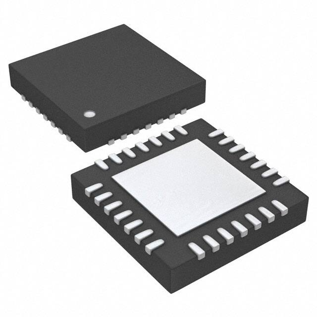


 工商网监
湘ICP备2023018690号
工商网监
湘ICP备2023018690号
