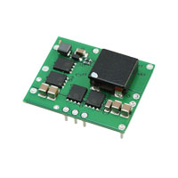
PTH05030W —5-V Input
30-A, 5-V Input Non-Isolated
Wide-Output Adjust Power Modules
SLTS210B – MAY 2003 – REVISED JANUARY 2004
Features
NOMINAL SIZE =
• Up to 30 A Output Current
• 5-V Input Voltage
• Wide-Output Voltage Adjust
(0.8 V to 3.6 V)
• 180 W/in³ Power Density
• On/Off Inhibit
• Efficiencies up to 94 %
• Pre-Bias Startup
• Margin Up/Down Controls
• Under-Voltage Lockout
1.37 in x 1.12 in
(34,8 mm x 28,5 mm)
• Auto-Track™ Sequencing
• Output Over-Current Protection
(Non-Latching, Auto-Reset)
• Over-Temperature Protection
• Operating Temp: –40 to +85 °C
• Safety Agency Approvals:
UL 1950, CSA 22.2 950, EN60950
VDE (Pending)
• Point-of-Load Alliance (POLA)
Compatible
Description
Pin Configuration
put voltage of the PTH05030W can be
set to any value over the range 0.8 V to
3.6 V, using a single resistor.
This series includes Auto-Track™.
Auto-Track simplifies power-up and
power-down supply voltage sequencing
in a system by enabling modules to track
each other, or any other external voltage.
Each model also includes an on/off
inhibit, output voltage adjust (trim), and
margin up/down controls. An output
voltage sense ensures tight load regulation,
and an output over-current and thermal
shutdown feature provide for protection
against external load faults.
Package options inlude both throughhole and surface mount configurations.
The PTH05030 is a series of highcurrent non-isolated power modules
from Texas Instruments. This product is
characterized by high efficiencies, and
up to 30 A of output current, while occupying a mere 1.64 in² of PCB area. In
terms of cost, size, and performance, the
series provides OEM’s with a flexible
module that meets the requirements of
the most complex and demanding mixedsignal applications. These include the
most densly populated, multi-processor
systems that incorporate high-speed
DSP’s, microprocessors, and ASICs.
The series uses double-sided surface
mount construction and provides highperformance step-down power conversion
from a 5-V input bus voltage. The out-
Pin
1
2
3
4
5
6
7
8
9
10
11
12
13
Function
GND
Vin
GND
Inhibit *
Vo Adjust
Vo Sense
GND
Vout
Vout
GND
Track
Margin Down *
Margin Up *
* Denotes negative logic:
Open
= Normal operation
Ground = Function active
ack™
r
T
o
t
Au
ncing
e
u
q
e
S
Standard Application
Track
Rset = Required to set the output voltage to a value
higher than 0.8 V. (see spec. table for values).
Cin = Required 1,500 µF capacitor.
Cout = Optional 330 µF capacitor.
Margin Down
Margin Up
13
12
11
1
V IN
2
10
PTH05030W
(Top View)
3
9
V OUT
8
7
4
5
6
Inhibit
V o Sense
+
GND
For technical support and further information, visit http://power.ti.com
RSET
0.5 %, 0.1 W
(Required)
COUT
330 µF
(Optional)
L
O
A
D
+
CIN
1,500 µF
(Required)
GND
�PTH05030W —5-V Input
30-A, 5-V Input Non-Isolated
Wide-Output Adjust Power Modules
SLTS210B – MAY 2003 – REVISED JANUARY 2003
Ordering Information
Output Voltage (PTH05030Hxx)
Package Options (PTH05030xHH) (1)
Code
W
Code
AH
AS
Voltage
0.8 V – 3.6 V (Adjust)
Description
Horiz. T/H
SMD, Standard (3)
Pkg Ref. (2)
(EUM)
(EUN)
Notes: (1) Add “T” to end of part number for tape and reel on SMD packages only.
(2) Reference the applicable package reference drawing for the dimensions and PC board layout
(3) “Standard” option specifies 63/37, Sn/Pb pin solder material.
Pin Descriptions
Vin: The positive input voltage power node to the module, which is referenced to common GND.
Vout: The regulated positive power output with respect
to the GND node.
GND: This is the common ground connection for the
Vin and Vout power connections. It is also the 0 VDC
reference for the control inputs.
Inhibit: The Inhibit pin is an open-collector/drain negative
logic input that is referenced to GND. Applying a lowlevel ground signal to this input disables the module’s
output and turns off the output voltage. When the Inhibit
control is active, the input current drawn by the regulator is significantly reduced. If the Inhibit pin is left
open-circuit, the module will produce an output whenever a valid input source is applied.
Vo Adjust: A 0.1 W 1 % resistor must be directly connected
between this pin and pin 7 (GND) to set the output voltage
to a value higher than 0.8 V. The temperature stability of
the resistor should be 100 ppm/°C (or better). The set
point range for the output voltage is from 0.8 V to 3.6 V.
The resistor value required for a given output voltage
may be calculated from the following formula. If left
open circuit, the output voltage will default to its lowest
value. For further information on output voltage adjustment consult the related application note.
Rset
= 10 k ·
0.8 V
Vout – 0.8 V
– 2.49 k
The specification table gives the preferred resistor values
for a number of standard output voltages.
Vo Sense: The sense input allows the regulation circuit to
compensate for voltage drop between the module and
the load. For optimal voltage accuracy Vo Sense should
be connected to Vout. It can also be left disconnected.
Track: This is an analog control input that enables the
output voltage to follow an external voltage. This pin
becomes active typically 20 ms after the input voltage
has been applied, and allows direct control of the output
voltage from 0 V up to the nominal set-point voltage.
Within this range the output will follow the voltage at
the Track pin on a volt-for-volt basis. When the control
voltage is raised above this range, the module regulates
at its set-point voltage. The feature allows the output
voltage to rise simultaneously with other modules powered from the same input bus. If unused, this input should
be connected to Vin. Note: Due to the under-voltage lockout
feature, the output of the module cannot follow its own input
voltage during power up. For more information, consult the
related application note.
Margin Down: When this input is asserted to GND, the
output voltage is decreased by 5% from the nominal. The
input requires an open-collector (open-drain) interface.
It is not TTL compatible. A lower percent change can
be accomodated with a series resistor. For further information, consult the related application note.
Margin Up: When this input is asserted to GND, the
output voltage is increased by 5%. The input requires an
open-collector (open-drain) interface. It is not TTL
compatible. The percent change can be reduced with a
series resistor. For further information, consult the
related application note.
For technical support and further information, visit http://power.ti.com
�PTH05030W —5-V Input
30-A, 5-V Input Non-Isolated
Wide-Output Adjust Power Modules
SLTS210B – MAY 2003 – REVISED JANUARY 2004
Environmental & Absolute Maximum Ratings
Characteristics
Symbols
Track Input Voltage
Operating Temperature Range
Solder Reflow Temperature
Storage Temperature
Mechanical Shock
Vtrack
Ta
Treflow
Ts
Mechanical Vibration
Weight
Flammability
—
—
(Voltages are with respect to GND)
Conditions
Over Vin Range
Surface temperature of module body or pins
—
Per Mil-STD-883D, Method 2002.3
1 msec, ½ Sine, mounted
Mil-STD-883D, Method 2007.2
Suffix S
20-2000 Hz
Suffix H
Min
Typ
–0.3
–40
—
—
Max
Units
Vin + 0.3
85
235 (i)
125
V
°C
°C
°C
–40
—
—
500
—
G’s
—
—
—
10
20
10
—
—
—
grams
G’s
Meets UL 94V-O
Notes: (i) During reflow of SMD package version do not elevate peak temperature of the module, pins or internal components above the stated maximum.
Specifications
(Unless otherwise stated, T a =25 °C, V in =5 V, V out =3.3 V, C in =1,500 µF, Cout =0 µF, and I o =Iomax)
PTH05030W
Typ
Characteristics
Symbols
Conditions
Min
Output Current
Io
Input Voltage Range
Set-Point Voltage Tolerance
Temperature Variation
Line Regulation
Load Regulation
Total Output Variation
Vin
Vo tol
∆Regtemp
∆Regline
∆Regload
∆Regtot
60 °C, 200 LFM airflow
25 °C, natural convection
Over Io range
0
0
4.5
—
—
—
—
—
—
—
—
±0.5
±10
±12
30
30
5.5
±2
—
—
—
—
—
±3
Efficiency
η
—
—
—
—
—
—
—
—
94
93
90
89
87
86
40
47
—
—
—
—
—
—
—
—
—
—
—
—
—
—
—
3.4
70
100
±5
– 8 (3)
—
—
4.3
3.7
—
—
—
—
–130
1
4.45
—
Vin –0.5
–0.2
—
—
275
1,500 (5)
0
0
(8)
4
—
—
–130
10
300
—
330 (6)
—
—
Open
0.8
—
—
235
—
16,500
300
—
2.8
—
Vo Ripple (pk-pk)
Over-Current Threshold
Transient Response
Vr
Io trip
Margin Up/Down Adjust
Margin Input Current (pins 12 /13)
Track Input Current (pin 11)
Track Slew Rate Capability
Under-Voltage Lockout
ttr
∆Vtr
Vo adj
IIL margin
IIL track
dVtrack/dt
UVLO
Inhibit Control (pin4)
Input High Voltage
Input Low Voltage
Input Low Current
VIH
VIL
IIL inhibit
Input Standby Current
Switching Frequency
External Input Capacitance
External Output Capacitance
Iin inh
ƒs
Cin
Cout
Reliability
MTBF
–40 °C 5440 mA
10×10.5
10×12.7
3 [1]
2
Panasonic, Poly-Aluminum:
WA (SMD)
S/SE (SMD)
6.3 V
6.3 V
560
180
0.020 Ω
0.005 Ω
5100 mA
4000 mA
10×10.2
7.3×4.3×4.2
10 V
10 V
470
470
0.045 Ω
0.060 Ω
1723 mA
1826 mA
7.3L
×5.7W×4.1H
6.3 V
10 V
6.3 V
470
330
470
0.018 Ω
0.015 Ω
0.012 Ω
>1200 mA
>3800 mA
4200 mA
10 V
16 V
470
2200
0.100 Ω
0.015 Ω
1440 mA
9740 mA
Kemet, Ceramic X5R (SMD)
16 V
6.3 V
10
47
0.002 Ω
0.002 Ω
Murata, Ceramic X5R (SMD)
6.3 V
6.3 V
16 V
16 V
100
47
22
10
TDK, Ceramic X5R (SMD)
6.3 V
6.3 V
16 V
16 V
100
47
22
10
Panasonic:
FC (Radial)
FK (SMD)
United Chemi-con
FX, Oscon (Radial)
PXA, (Poly-Aluminum (SMD.)
LXZ, Aluminum (Radial)
AVX, Tantalum:
TPS (SMD)
Kemet (SMD):
T520, Poly-Tant
T530, Poly-Tant/Organic
Vishay-Sprague
595D, Tantalum (SMD)
94SA, Os-con (Radial)
Vendor Part Number
EEUFC1A561
EEUFC1C152S
EEVFK1C152Q
EEVFK1A222Q
6FX1000M
PXA6.3VC820MJ12TP
LXZ10VB681M10X12LL
LXZ10VB102M10X16LL
UHD0J102MPR
UPM1A152MHH6
≤3
≤2
10SP470M
6SVP820M
≤4
≤1
EEFWA0J561P
EEFSE0J181R
3 [ 1]
3 [ 1]
≤5
≤5
TPSE477M010R0045
TPSV477M010R0060
4.3W
×7.3L
×4.0H
3 [1]
5
3 [1]
≤5
≤3
≤2
T520X477M006SE018
T530X337M010AS
T530X477M006AS
7.2L×6W
×4.1H
16×25
3 [1]
1
≤5
≤3
595D477X0010R2T
94SA108X0016HBP
—
1210 case
3225 mm
1 [2]
1 [2]
≤5
≤5
C1210C106M4PAC
C1210C476K9PAC
0.002 Ω
—
1210 case
3225 mm
1 [2]
1 [2]
1 [2]
≤3
≤5
≤5
≤5
GRM32ER60J107M
GRM32ER60J476M
GRM32ER61C226K
GRM32DR61C106K
0.002 Ω
—
1210 case
3225 mm
1 [2]
1 [2]
1 [2]
≤3
≤5
≤5
≤5
C3225X5R0J107MT
C3225X5R0J476MT
C3225X5R1C226MT
C3225X5R1C106MT
3
N/ R
[1] The total capacitance is slightly lower than 1,500 µF, but is acceptable based on the combined ripple current rating.
[2] A ceramic capacitor may be used to complement electrolytic types at the input to further reduce high-frequency ripple current
For technical support and further information, visit http://power.ti.com
�Application Notes
PTH03030W & PTH05030W
Adjusting the Output Voltage of the PTH03030W &
PTH05030W Wide-Output Adjust Power Modules
The Vo Adjust control (pin 4) sets the output voltage of the
PTH03030W and PTH05030W products to a value higher
than 0.8 V. The adjustment range of the PT03030W
(3.3-V input) is from 0.8 V to 2.5 V 1, and the PTH05030W
(5-V input) from 0.8 V to 3.6 V. For an output voltage
other than 0.8 V a single external resistor, Rset, must be
connected directly between the Vo Adjust and GND pins 2.
Table 2-1 gives the preferred value of the external resistor
for a number of standard voltages, along with the actual
output voltage that this resistance value provides.
For other output voltages the value of the required resistor
can either be calculated using the following formula, or
simply selected from the range of values given in Table 2-2.
Figure 2-1 shows the placement of the required resistor.
Rset
= 10 kΩ ·
0.8 V
Vout – 0.8 V
– 2.49 kΩ
Table 2-1; Preferred Values of Rset for Standard Output Voltages
Vout (Standard)
Rset (Pref’d Value)
3.3 V 1
2.5 V
2V
1.8 V
1.5 V
1.2 V
1V
0.8 V
698 Ω
2.21 kΩ
4.12 kΩ
5.49 kΩ
8.87 kΩ
17.4 kΩ
36.5 kΩ
Open
Vout (Actual)
3.309V
2.502 V
2.010 V
1.803 V
1.504 V
1.202 V
1.005 V
0.8 V
Figure 2-1; Vo Adjust Resistor Placement
Vo Sense
13
12
11
Table 2-2; Output Voltage Set-Point Resistor Values
Va Req’d
0.800
0.825
0.850
0.875
0.900
0.925
0.950
0.975
1.000
1.025
1.050
1.075
1.100
1.125
1.150
1.175
1.200
1.225
1.250
1.275
1.300
1.325
1.350
1.375
1.400
1.425
1.450
1.475
1.50
1.55
1.60
1.65
1.70
1.75
1.80
1.85
1.90
1.95
Rset
Open
318 kΩ
158 kΩ
104 kΩ
77.5 kΩ
61.5 kΩ
50.8 kΩ
43.2 kΩ
37.5 kΩ
33.1 kΩ
29.5 kΩ
26.6 kΩ
24.2 kΩ
22.1 kΩ
20.4 kΩ
18.8 kΩ
17.5 kΩ
16.3 kΩ
15.3 kΩ
14.4 kΩ
13.5 kΩ
12.7 kΩ
12.1 kΩ
11.4 kΩ
10.8 kΩ
10.3 kΩ
9.82 kΩ
9.36 kΩ
8.94 kΩ
8.18 kΩ
7.51 kΩ
6.92 kΩ
6.4 kΩ
5.93 kΩ
5.51 kΩ
5.13 kΩ
4.78 kΩ
4.47 kΩ
Va Req’d
2.00
2.05
2.10
2.15
2.20
2.25
2.30
2.35
2.40
2.45
2.50
2.55
2.60
2.65
2.70
2.75
2.80
2.85
2.90
2.95
3.00
3.05
3.10
3.15
3.20
3.25
3.30
3.35
3.40
3.45
3.50
3.55
3.60
Rset
4.18 kΩ
3.91 kΩ
3.66 kΩ
3.44 kΩ
3.22 kΩ
3.03 kΩ
2.84 kΩ
2.67 kΩ
2.51 kΩ
2.36 kΩ
2.22 kΩ
2.08 kΩ
1.95 kΩ
1.83 kΩ
1.72 kΩ
1.61 kΩ
1.51 kΩ
1.41 kΩ
1.32 kΩ
1.23 kΩ
1.15 kΩ
1.07 kΩ
988 Ω
914 Ω
843 Ω
775 Ω
710 Ω
647 Ω
587 Ω
529 Ω
473 Ω
419 Ω
367 Ω
6
Sense
PTH05030W
GND
1, 3, 7
VO
8, 9
VOUT
G N D Adjust
10
5
R SET
1 %, 0.1 W
GND
For technical support and further information, visit http://power.ti.com
COUT
330 µF
(Optional)
GND
Notes:
1. Modules that operate from a 3.3-V input bus should
not be adjusted higher than 2.5 V.
2. Use a 0.1 W resistor. The tolerance should be 1 %, with
temperature stability of 100 ppm/°C (or better). Place
the resistor as close to the regulator as possible. Connect
the resistor directly between pins 5 and 10 using dedicated
PCB traces.
3. Never connect capacitors from Vo Adjust to either GND or
Vout. Any capacitance added to the Vo Adjust pin will affect
the stability of the regulator.
�Application Notes
PTH Series of Wide-Output Adjust
Power Modules (3.3/5-V Input)
Point-of-Load Alliance
The PTH family of non-isolated, wide-output adjust
power modules from Texas Instruments are optimized
for applications that require a flexible, high performance
module that is small in size. These products are part of
the “Point-of-Load Alliance” (POLA), which ensures
compatible footprint, interoperability and true second
sourcing for customer design flexibility. The POLA is a
collaboration between Texas Instruments, Artesyn Technologies, and Astec Power to offer customers advanced
non-isolated modules that provide the same functionality
and form factor. Product series covered by the alliance
includes the PTHxx050W (6 A), PTHxx060W (10 A),
PTHxx010W (15/12 A), PTHxx020W (22/18 A), and
the PTHxx030W (30/26 A).
From the basic, “Just Plug it In” functionality of the 6-A
modules, to the 30-A rated feature-rich PTHxx030W,
these products were designed to be very flexible, yet simple
to use. The features vary with each product. Table 3-1
provides a quick reference to the available features by
product and input bus voltage.
output current, PTHxx020W and PTHxx030W products
incorporate over-temperature shutdown protection. All
of the products referenced in Table 3-1 include AutoTrack™. This is a feature unique to the PTH family,
and was specifically designed to simplify the task of sequencing the supply voltage in a power system. These
and other features are described in the following sections.
Soft-Start Power Up
The Auto-Track feature allows the power-up of multiple
PTH modules to be directly controlled from the Track
pin. However in a stand-alone configuration, or when
the Auto-Track feature is not being used, the Track pin
should be directly connected to the input voltage, Vin
(see Figure 3-1).
Figure 3–1
10
Up
5V
2
Inhibit
3
12 V
8A
3.3 V / 5 V
15 A
12 V
12 A
3.3 V / 5 V
22 A
12 V
18 A
3.3 V / 5 V
30 A
12 V
26 A
Pre-Bias Startup
•
•
•
•
•
•
Thermal Shutdown
10 A
•
•
•
•
•
•
•
•
•
•
Output Sense
PTHxx030
6A
3.3 V / 5 V
•
•
•
•
•
•
•
•
•
•
Margin Up/Down
PTHxx020
12 V
•
•
•
•
•
•
•
•
•
•
Auto-Track™
PTHxx010
6A
Over-Current
PTHxx060
I OUT
On/Off Inhibit
PTHxx050
Input Bus
3.3 V / 5 V
Adjust (Trim)
+
Series
•
•
•
•
•
•
•
•
•
•
•
•
•
•
•
•
•
•
•
•
•
•
•
•
•
•
•
•
•
•
CIN
1,000 µF
8
5
Track
Sense
PTH05020W
V IN
Table 3-1; Operating Features by Series and Input Bus Voltage
9
Dn
3.3 V
6
Adjust
GND
1
VO
7
4
R SET, 698 Ω
0.1 W, 1 %
+
Features of the PTH Family of Non-Isolated
Wide Output Adjust Power Modules
C OUT
330 µF
GND
GND
When the Track pin is connected to the input voltage the
Auto-Track function is permanently disengaged. This
allows the module to power up entirely under the control
of its internal soft-start circuitry. When power up is under
soft-start control, the output voltage rises to the set-point
at a quicker and more linear rate.
Figure 3–2
Vin (1 V/Div)
Vout (1 V/Div)
For simple point-of-use applications, the PTHxx050W
provides operating features such as an on/off inhibit,
output voltage trim, pre-bias startup (3.3/5-V input only),
and over-current protection. The PTHxx060W (10 A),
and PTHxx010W (15/12 A) include an output voltage
sense, and margin up/down controls. Then the higher
Iin (5 A/Div)
HORIZ SCALE: 5 ms/Div
For technical support and further information visit http://power.ti.com
�Application Notes
PTH Series of Wide-Output Adjust
Power Modules (3.3/5-V Input)
The power modules function normally when the Inhibit
pin is left open-circuit, providing a regulated output
whenever a valid source voltage is connected to Vin with
respect to GND.
Figure 3-3 shows the typical application of the inhibit
function. Note the discrete transistor (Q1). The Inhibit
control has its own internal pull-up to Vin potential. The
input is not compatible with TTL logic devices. An opencollector (or open-drain) discrete transistor is recommended
for control.
Figure 3–3
V o Sense
Over-Current Protection
Over-Temperature Protection
The PTHxx020 and PTHxx030 series of products have
over-temperature protection. These products have an
on-board temperature sensor that protects the module’s
internal circuitry against excessively high temperatures.
A rise in the internal temperature may be the result of a
drop in airflow, or a high ambient temperature. If the
internal temperature exceeds the OTP threshold, the
module’s Inhibit control is automatically pulled low. This
turns the output off. The output voltage will drop as the
external output capacitors are discharged by the load
circuit. The recovery is automatic, and begins with a
soft-start power up. It occurs when the the sensed temperature decreases by about 10 °C below the trip point.
10
VIN
2
8
5
1
7
Q1
BSS138
VOUT
6
4
RSET
COUT
330 µF
L
O
A
D
1 =Inhibit
GND
GND
Turning Q1 on applies a low voltage to the Inhibit control
and disables the output of the module. If Q1 is then turned
off, the module will execute a soft-start power-up. A
regulated output voltage is produced within 20 msec.
Figure 3-4 shows the typical rise in both the output voltage and input current, following the turn-off of Q1. The
turn off of Q1 corresponds to the rise in the waveform,
Q1 Vds. The waveforms were measured with a 5-A load.
Figure 3–4
Note: The over-temperature protection is a last resort mechanism to prevent thermal stress to the regulator. Operation at
or close to the thermal shutdown temperature is not recommended and will reduce the long-term reliability of the module.
Always operate the regulator within the specified Safe Operating
Area (SOA) limits for the worst-case conditions of ambient
temperature and airflow.
Vo (2V/Div)
Iin (2A/Div)
Output On/Off Inhibit
For applications requiring output voltage on/off control,
each series of the PTH family incorporates an output
Inhibit control pin. The inhibit feature can be used wherever there is a requirement for the output voltage from
the regulator to be turned off.
9
PTH05020W
3
CIN
1,000 µF
+
For protection against load faults, all modules incorporate
output over-current protection. Applying a load that
exceeds the regulator’s over-current threshold will cause
the regulated output to shut down. Following shutdown
a module will periodically attempt to recover by initiating
a soft-start power-up. This is described as a “hiccup” mode
of operation, whereby the module continues in a cycle of
successive shutdown and power up until the load fault is
removed. During this period, the average current flowing
into the fault is significantly reduced. Once the fault is
removed, the module automatically recovers and returns
to normal operation.
+
From the moment a valid input voltage is applied, the
soft-start control introduces a short time delay (typically
5 ms-10 ms) before allowing the output voltage to rise.
The output then progressively rises to the module’s setpoint voltage. Figure 3-2 shows the soft-start power-up
characteristic of the 22-A output product (PTH05020W),
operating from a 5-V input bus and configured for a 3.3-V
output. The waveforms were measured with a 5-A resistive
load, with Auto-Track disabled. The initial rise in input
current when the input voltage first starts to rise is the
charge current drawn by the input capacitors. Power-up
is complete within 15 ms.
Q1Vds (5V/Div)
HORIZ SCALE: 10ms/Div
For technical support and further information visit http://power.ti.com
�Application Notes
PTH Series of Wide-Output Adjust
Power Modules (3.3/5-V Input)
Auto-Track™ Function
The Auto-Track function is unique to the PTH family,
and is available with the all “Point-of-Load Alliance”
(POLA) products. Auto-Track was designed to simplify
the amount of circuitry required to make the output
voltage from each module power up and power down in
sequence. The sequencing of two or more supply voltages
during power up is a common requirement for complex
mixed-signal applications, that use dual-voltage VLSI ICs
such as DSPs, micro-processors, and ASICs.
How Auto-Track Works
Auto-Track works by forcing the module’s output voltage
to follow a voltage presented at the Track control pin. This
control range is limited to between 0 V and the module’s
set-point voltage. Once the track-pin voltage is raised
above the set-point voltage, the module’s output remains
at its set-point 1. As an example, if the Track pin of a 2.5-V
regulator is at 1 V, the regulated output will be 1 V. But
if the voltage at the Track pin rises to 3 V, the regulated
output will not go higher than 2.5 V.
When under track control, the regulated output from
the module follows the voltage at its Track pin on a voltfor-volt basis. By connecting the Track pin of a number
of these modules together, the output voltages will follow a common signal during power-up and power-down.
The control signal can be an externally generated master
ramp waveform, or the output voltage from another power
supply circuit 3. For convenience the Track control incorporates an internal RC charge circuit. This operates off
the module’s input voltage to provide a suitable rising
voltage ramp waveform.
Typical Application
The basic implementation of Auto-Track allows for
simultaneous voltage sequencing of a number of AutoTrack compliant modules. Connecting the Track control
pins of two or more modules forces the Track control of
all modules to follow the same collective RC ramp waveform, and allows them to be controlled through a single
transistor or switch; Q1 in Figure 3-5.
To initiate a power-up sequence the Track control must
first pulled to ground potential. This should be done at
or before input power is applied to the modules, and then
held for at least 10 ms thereafter. This brief period gives
the modules time to complete their internal soft-start
initialization, which enables them to produce an output
voltage.
Applying a logic-level high signal to the circuit’s On/Off
Control turns Q1 on and applies a ground signal to the
Track control. After completing their internal soft-start
intialization, the output of all modules will remain at zero
volts while Q1 is on. 10 ms after a valid input voltage has
been applied to all modules, Q1 can be turned off. This
allows the track control voltage to automatically rise
toward to the modules' input voltage. During this period
the output voltage of each module will rise in unison with
For technical support and further information visit http://power.ti.com
other modules, to its respective set-point voltage.
Figure 3-6 shows the output voltage waveforms from the
circuit of Figure 3-5 after the On/Off Control is set from a
high to a low-level voltage. The waveforms, Vo1 and Vo2
represent the output voltages from the two power modules, U1 (3.3 V) and U2 (1.8 V) respectively. Vo1 and Vo2
are shown rising together to produce the desired simultaneous power-up characteristic.
The same circuit also provides a power-down sequence.
Power down is the reverse of power up, and is accomplished by lowering the track control voltage back to zero
volts. The important constraint is that a valid input voltage
must be maintained until the power down is complete. It
also requires that Q1 be turned off relatively slowly. This
is so that the Track control voltage does not fall faster than
Auto-Track's slew rate capability, which is 1 V/ms. The
components R1 and C1 in Figure 3-5 limit the rate at
which Q1 can pull down the Track control voltage. The
values of 100 k-ohm and 0.1 µF correlate to a decay rate
of about 0.17 V/ms.
The power-down sequence is initiated with a low-to-high
transition at the On/Off Control input to the circuit.
Figure 3-7 shows the power-down waveforms. As the
Track control voltage falls below the nominal set-point
voltage of each power module, then its output voltage
decays with all the other modules under Auto-Track
control.
Notes on Use of Auto-Track™
1. The Track pin voltage must be allowed to rise above
the module’s set-point voltage before the module can
regulate at its adjusted set-point voltage.
2. The Auto-Track function will track almost any voltage
ramp during power up, and is compatible with ramp
speeds of up to 1 V/ms.
3. The absolute maximum voltage that may be applied to the
Track pin is Vin.
4. The module will not follow a voltage at its Track control
input until it has completed its soft-start initialization.
This takes about 10 ms from the time that the module
has sensed that a valid voltage has been applied its input.
During this period, it is recommended that the Track
pin be held at ground potential.
5. The module is capable of both sinking and sourcing
current when following a voltage at its Track pin.
Therefore startup into an output prebias is not supported
during Auto-Track control. Note: A pre-bias holdoff is
not necessary when all supply voltages rise simultaneously
under the control of Auto-Track.
6. The Auto-Track function can be disabled by connecting
the Track pin to the input voltage (Vin). With Auto-Track
disabled, the output voltage will rise at a quicker and
more linear rate after input power is applied.
�Application Notes
PTH Series of Wide-Output Adjust
Power Modules (3.3/5-V Input)
Figure 3–5; Sequenced Power Up & Power Down Using Auto-Track
U1
10
9
8
5
Track
PTH05020W
VIN
Inhibit
Vo1 =3.3 V
6
GND
+
3
C IN
VO
1
+
2
+5 V
4
7
C OUT
R2
698
C1
0.1 µF
U2
R1
100 k
9
8
5
Track
2
+
C IN
0V
Figure 3–6; Simultaneous Power Up with Auto-Track Control
HORIZ SCALE: 10 ms/Div
10
Q1
BSS138
PTH05010W
VIN
Inhibit
3
VO
Vo2 =1.8 V
6
GND
1
7
4
R3
5k49
+
On/Off Control
1 = Power Down
0 = Power Up
C OUT
Figure 3–7; Simultaneous Power Down with Auto-Track Control
Vo1 (1 V/Div)
Vo1 (1 V/Div)
Vo2 (1 V/Div)
Vo2 (1 V/Div)
On/Off Input
(5 V/Div)
On/Off Input
(5 V/Div)
HORIZ SCALE: 10 ms/Div
For technical support and further information visit http://power.ti.com
�Application Notes
PTH Series of Wide-Output Adjust
Power Modules (3.3/5-V Input)
Margin Up/Down Controls
Notes:
The PTHxx060W, PTHxx010W, PTHxx020W, and
PTHxx030W products incorporate Margin Up and Margin
Down control inputs. These controls allow the output
voltage to be momentarily adjusted 1, either up or down,
by a nominal 5 %. This provides a convenient method
for dynamically testing the operation of the load circuit
over its supply margin or range. It can also be used to verify
the function of supply voltage supervisors. The ±5 %
change is applied to the adjusted output voltage, as set by
the external resistor, Rset at the Vo Adjust pin.
The 5 % adjustment is made by pulling the appropriate
margin control input directly to the GND terminal 2.
A low-leakage open-drain device, such as an n-channel
MOSFET or p-channel JFET is recommended for this
purpose 3. Adjustments of less than 5 % can also be accommodated by adding series resistors to the control inputs.
The value of the resistor can be selected from Table 3-2,
or calculated using the following formula.
Up/Down Adjust Resistance Calculation
1. The Margin Up* and Margin Dn* controls were not
intended to be activated simultaneously. If they are
their affects on the output voltage may not completely
cancel, resulting in the possibility of a slightly higher
error in the output voltage set point.
2. The ground reference should be a direct connection to
the module GND at pin 7 (pin 1 for the PTHxx050).
This will produce a more accurate adjustment at the
load circuit terminals. The transistors Q1 and Q2 should
be located close to the regulator.
3. The Margin Up and Margin Dn control inputs are not
compatible with devices that source voltage. This includes
TTL logic. These are analog inputs and should only be
controlled with a true open-drain device (preferably
a discrete MOSFET transistor). The device selected
should have low off-state leakage current. Each input
sources 8 µA when grounded, and has an open-circuit
voltage of 0.8 V.
To reduce the margin adjustment to something less than
5 %, series resistors are required (See RD and RU in
Figure 3-8). For the same amount of adjustment, the
resistor value calculated for RU and RD will be the same.
The formulas is as follows.
RU or RD =
499
∆%
– 99.8
Table 3-2; Margin Up/Down Resistor Values
% Adjust
5
4
3
2
1
kΩ
Where ∆% = The desired amount of margin adjust in
percent.
RU / RD
0.0 kΩ
24.9 kΩ
66.5 kΩ
150.0 kΩ
397.0 kΩ
Figure 3–8; Margin Up/Down Application Schematic
10
9
8
1
7
0V
PTH05010W
(Top View)
VIN
2
RD
4
5
RU
RSET
0.1 W, 1 %
Cin
MargDn
+VOUT
6
3
+
+Vo
+
Cout
L
O
A
D
Q1
MargUp
GND
For technical support and further information visit http://power.ti.com
Q2
GND
�Application Notes
PTH Series of Wide-Output Adjust
Power Modules (3.3/5-V Input)
Pre-Bias Startup Capability
Notes
Only selected products in the PTH family incorporate this
capability. Consult Table 3-1 to identify which products
are compliant.
1. Startup includes the short delay (approx. 10 ms) prior
to the output voltage rising, followed by the rise of the
output voltage under the module’s internal soft-start
control. Startup is complete when the output voltage
has risen to either the set-point voltage or the voltage
at the Track pin, whichever is lowest.
A pre-bias startup condition occurs as a result of an external
voltage being present at the output of a power module prior
to its output becoming active. This often occurs in complex digital systems when current from another power
source is backfed through a dual-supply logic component,
such as an FPGA or ASIC. Another path might be via
clamp diodes as part of a dual-supply power-up sequencing
arrangement. A prebias can cause problems with power
modules that incorporate synchronous rectifiers. This is
because under most operating conditions, these types of
modules can sink as well as source output current.
2. To ensure that the regulator does not sink current when
power is first applied (even with a ground signal applied
to the Inhibit control pin), the input voltage must always
be greater than the output voltage throughout the
power-up and power-down sequence.
3. The Auto-Track function can be disabled at power up
by immediately applying a voltage to the module’s Track
pin that is greater than its set-point voltage. This can
be easily accomplished by connecting the Track pin to
Vin.
The PTH family of power modules incorporate synchronous rectifiers, but will not sink current during startup 1,
or whenever the Inhibit pin is held low. However, to ensure
satisfactory operation of this function, certain conditions
must be maintained. 2 Figure 3-9 shows an application
demonstrating the pre-bias startup capability. The startup waveforms are shown in Figure 3-10. Note that the
output current from the PTH03010W (Io) shows negligible current until its output voltage rises above that
backfed through diodes D1 and D2.
Figure 3–10; Pre-Bias Startup Waveforms
Vin (1 V/Div)
Vo (1 V/Div)
Note: The pre-bias start-up feature is not compatible with
Auto-Track. When the module is under Auto-Track control,
it will sink current if the output voltage is below that of a
back-feeding source. To ensure a pre-bias hold-off one of two
approaches must be followed when input power is applied to
the module. The Auto-Track function must either be disabled 3,
or the module’s output held off (for at least 50 ms) using the
Inhibit pin. Either approach ensures that the Track pin voltage is above the set-point voltage at start up.
Io (5 A/Div)
HORIZ SCALE: 5 ms/Div
Figure 3–9; Application Circuit Demonstrating Pre-Bias Startup
VIN = 3.3 V
10
2
3
CIN
330 µF
8
5
Track
Sense
PTH03010W
V IN
Inhibit
+
9
GND
1
VO
Vo = 2.5 V
6
+
Vadj
7
Io
4
R2
2k21
VCCIO
VCORE
+
C OUT
330 µF
ASIC
For technical support and further information visit http://power.ti.com
�Application Notes
PTH Series of Wide-Output Adjust
Power Modules (3.3/5-V Input)
Remote Sense
The PTHxx060W, PTHxx010W, PTHxx020W, and
PTHxx030W products incorporate an output voltage
sense pin, Vo Sense. The Vo Sense pin should be connected
to Vout at the load circuit (see data sheet standard application). A remote sense improves the load regulation
performance of the module by allowing it to compensate
for any ‘IR’ voltage drop between itself and the load. An
IR drop is caused by the high output current flowing
through the small amount of pin and trace resistance.
Use of the remote sense is optional. If not used, the
V o Sense pin can be left open-circuit. An internal lowvalue resistor (15-Ω or less) is connected between the
Vo Sense and Vout. This ensures the output voltage remains
in regulation.
With the sense pin connected, the difference between
the voltage measured directly between the Vout and GND
pins, and that measured from V o Sense to GND, is the
amount of IR drop being compensated by the regulator.
This should be limited to a maximum of 0.3 V.
Note: The remote sense feature is not designed to compensate
for the forward drop of non-linear or frequency dependent
components that may be placed in series with the converter
output. Examples include OR-ing diodes, filter inductors,
ferrite beads, and fuses. When these components are enclosed
by the remote sense connection they are effectively placed
inside the regulation control loop, which can adversely affect
the stability of the regulator.
For technical support and further information visit http://power.ti.com
�PACKAGE OPTION ADDENDUM
www.ti.com
20-Mar-2022
PACKAGING INFORMATION
Orderable Device
Status
(1)
Package Type Package Pins Package
Drawing
Qty
Eco Plan
(2)
Lead finish/
Ball material
MSL Peak Temp
Op Temp (°C)
(3)
Device Marking
(4/5)
(6)
PTH05030WAD
ACTIVE
ThroughHole Module
EUM
13
16
RoHS Exempt
& Green
SN
N / A for Pkg Type
-40 to 85
PTH05030WAH
ACTIVE
ThroughHole Module
EUM
13
16
RoHS Exempt
& Green
SN
N / A for Pkg Type
-40 to 85
PTH05030WAS
ACTIVE
Surface
Mount Module
EUN
13
16
Non-RoHS
& Green
SNPB
Level-1-235C-UNLIM/
Level-3-260C-168HRS
-40 to 85
PTH05030WAST
ACTIVE
Surface
Mount Module
EUN
13
200
Non-RoHS
& Green
SNPB
Level-1-235C-UNLIM/
Level-3-260C-168HRS
-40 to 85
PTH05030WAZ
ACTIVE
Surface
Mount Module
EUN
13
16
RoHS (In
Work) & Green
SNAGCU
Level-3-260C-168 HR
-40 to 85
PTH05030WAZT
ACTIVE
Surface
Mount Module
EUN
13
200
RoHS (In
Work) & Green
SNAGCU
Level-3-260C-168 HR
-40 to 85
(1)
The marketing status values are defined as follows:
ACTIVE: Product device recommended for new designs.
LIFEBUY: TI has announced that the device will be discontinued, and a lifetime-buy period is in effect.
NRND: Not recommended for new designs. Device is in production to support existing customers, but TI does not recommend using this part in a new design.
PREVIEW: Device has been announced but is not in production. Samples may or may not be available.
OBSOLETE: TI has discontinued the production of the device.
(2)
RoHS: TI defines "RoHS" to mean semiconductor products that are compliant with the current EU RoHS requirements for all 10 RoHS substances, including the requirement that RoHS substance
do not exceed 0.1% by weight in homogeneous materials. Where designed to be soldered at high temperatures, "RoHS" products are suitable for use in specified lead-free processes. TI may
reference these types of products as "Pb-Free".
RoHS Exempt: TI defines "RoHS Exempt" to mean products that contain lead but are compliant with EU RoHS pursuant to a specific EU RoHS exemption.
Green: TI defines "Green" to mean the content of Chlorine (Cl) and Bromine (Br) based flame retardants meet JS709B low halogen requirements of


 工商网监
湘ICP备2023018690号
工商网监
湘ICP备2023018690号
