PTH08080W
www.ti.com
SLTS235D – FEBRUARY 2005 – REVISED SEPTEMBER 2013
2.25-A, WIDE-INPUT ADJUSTABLE SWITCHING REGULATOR
Check for Samples: PTH08080W
FEATURES
DESCRIPTION
•
•
•
The PTH08080W is a highly integrated, low-cost
switching regulator module that delivers up to 2.25 A
of output current. The PTH08080W sources output
current at a much higher efficiency than a TO-220
linear regulator IC, thereby eliminating the need for a
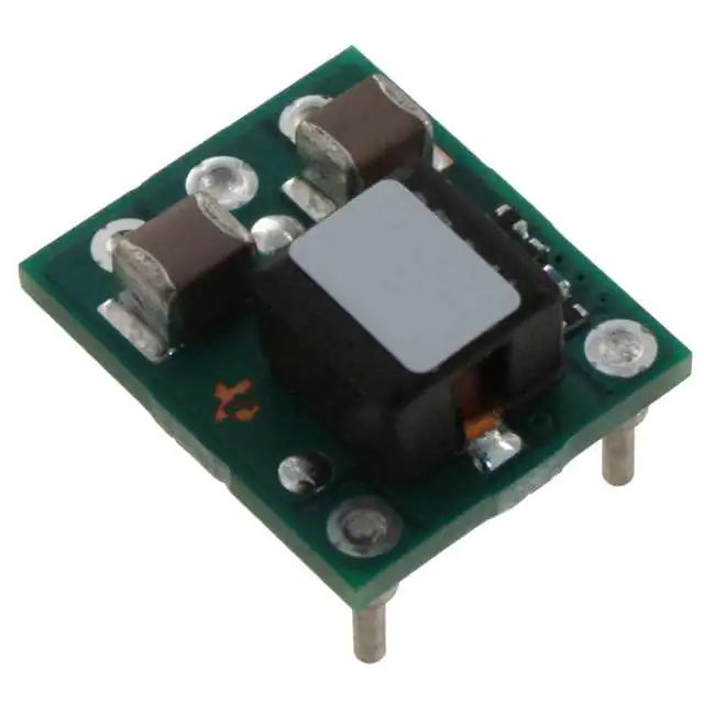
heat sink. Its small size (0.5 × 0.6 in) and flexible
operation creates value for a variety of applications.
1
•
•
•
•
•
•
•
•
Up to 2.25-A Output Current at 85°C
4.5-V to 18-V Input Voltage Range
Wide-Output Voltage Adjust
(0.9 V to 5.5 V)
Efficiencies Up To 93%
On/Off Inhibit
Undervoltage Lockout (UVLO)
Output Overcurrent Protection
(Nonlatching, Auto-Reset)
Overtemperature Protection
Ambient Temperature Range: –40°C to 85°C
Surface-Mount Package
Safety Agency Approvals:
UL/CUL 60950, EN60950
APPLICATIONS
•
Telecommunications, Instumentation,
and General-Purpose Circuits
The input voltage range of the PTH08080W is from
4.5 V to 18 V, allowing operation from either a 5-V or
12-V input bus. Using state-of-the-art switched-mode
power-conversion technology, the PTH08080W can
step down to voltages as low as 0.9 V from a 5-V
input bus, with less than 1 W of power dissipation.
The output voltage can be adjusted to any voltage
over the range, 0.9 V to 5.5 V, using a single external
resistor. Operating features include an undervoltage
lockout (UVLO), on/off inhibit, overcurrent protection,
and overtemperature protection. Target applications
include telecommunications, test and measurement
applications, and high-end consumer products. This
product is available in both through-hole and surfacemount package options, including tape and reel.
STANDARD APPLICATION
Inhibit
D1$
5
4
RSET #
0.05 W, 1%
(Required)
PTH08080W
(Top View )
VI
+
GND
VO
3
1
CI *
100 mF
Electrolytic
2
(Required)
CO *
100 mF
Electrolytic
(Optional)
GND
* See The Capacitor Application Information
# See the Specification Table for the RSET value.
$ Diode is Required When VO > 5.25 V and VI > 16 V.
1
Please be aware that an important notice concerning availability, standard warranty, and use in critical applications of
Texas Instruments semiconductor products and disclaimers thereto appears at the end of this data sheet.
PRODUCTION DATA information is current as of publication date.
Products conform to specifications per the terms of the Texas
Instruments standard warranty. Production processing does not
necessarily include testing of all parameters.
Copyright © 2005–2013, Texas Instruments Incorporated
�PTH08080W
SLTS235D – FEBRUARY 2005 – REVISED SEPTEMBER 2013
www.ti.com
This integrated circuit can be damaged by ESD. Texas Instruments recommends that all integrated circuits be handled with
appropriate precautions. Failure to observe proper handling and installation procedures can cause damage.
ESD damage can range from subtle performance degradation to complete device failure. Precision integrated circuits may be more
susceptible to damage because very small parametric changes could cause the device not to meet its published specifications.
ORDERING INFORMATION
For the most current package and ordering information, see the Package Option Addendum at the end of this datasheet, or see
the TI website at www.ti.com.
ABSOLUTE MAXIMUM RATINGS
over operating free-air temperature range unless otherwise noted (1)
TA
Operating free-air
temperature
Over VI range
Wave Solder
temperature
TS
Solder reflow
temperature
Surface temperature of module body or pins
Tstg Storage temperature
(1)
PTH08080W
UNIT
–40 to 85
°C
Suffix AH
235
Suffix AD
260
Suffix AS
235
Suffix AZ
260
°C
–55 to 125
°C
Stresses beyond those listed under absolute maximum ratings may cause permanent damage to the device. These are stress ratings
only, and functional operation of the device at these or any other conditions beyond those indicated under recommended operating
conditions is not implied. Exposure to absolute-maximum-rated conditions for extended periods may affect device reliability.
RECOMMENDED OPERATING CONDITIONS
MIN
MAX
UNIT
VI
Input voltage
4.5
18
V
TA
Operating free-air temperature
–40
85
°C
PACKAGE SPECIFICATIONS
PTH08080W (Suffix AH and AS)
Weight
Flammability
Mechanical shock
Mechanical vibration
(1)
2
1.5 grams
Meets UL 94 V-O
Per Mil-STD-883D, Method 2002.3, 1 ms, 1/2 sine, mounted
Mil-STD-883D, Method 2007.2, 20-2000 Hz
500 G
20 G
(1)
(1)
Qualification limit.
Submit Documentation Feedback
Copyright © 2005–2013, Texas Instruments Incorporated
Product Folder Links :PTH08080W
�PTH08080W
www.ti.com
SLTS235D – FEBRUARY 2005 – REVISED SEPTEMBER 2013
ELECTRICAL CHARACTERISTICS
at 25°C free-air temperature, VI = 12 V, VO = 3.3 V, IO = IOmax, CI = 100 µF, CO = 100 µF (unless otherwise noted)
PARAMETER
TEST CONDITIONS
MIN
IO
Output current
TA = 85°C, natural convection airflow
0
PO
Output power
TA = 85°C, natural convection airflow
Set-point voltage tolerance
TA = 25°C
Temperature variation
-40 ≤ TA ≤ +85°C
Line regulation
Over VI range
±7
mV
Load regulation
Over IO range
±0.13
%Vo
Total output voltage variation
Includes set-point, line, load, -40 ≤ TA ≤ +85°C
Output Voltage Adjust Range
Over IO range
VO
VADJ
VI
Input Voltage Range
Efficiency
Over VO range
TA = 25°C,
IO = 2 A
UVLO
UNIT
2.25
A
10
W
(1)
%
±0.5
%Vo
(1)
3
0.9
5.5
0.9 V ≤ VO ≤ 1.8 V
4.5
VO x 10 (2)
1.8 V < VO ≤ 3.4 V
4.5
18
3.4 V < VO ≤ 5.5 V
(2)
(2)
VO + 1.1
18
%Vo
V
V
93.5%
RSET = 1.87 kΩ, VO = 3.3 V
92%
RSET = 3.74 kΩ, VO = 2.5 V
91%
RSET = 6.19 kΩ, VO = 2 V
90%
RSET = 8.06 kΩ, VO = 1.8 V
IO (trip)
MAX
±2
RSET = 348 Ω, VO = 5 V
η
TYP
89%
RSET = 13 kΩ, VO = 1.5 V
87.5%
RSET = 27.4 kΩ, VO = 1.2 V
86.5%
Output voltage ripple
20 MHz bandwith
30
Overcurrent threshold
Reset, followed by autorecovery
3.5
A
Recovery time
50
µs
Transient response
CO = 100 µF, 1
A/µs load step
from 50% to 100%
IOmax
VO over/undershoot
70
mV
Undervoltage lockout
VI = increasing
VI = decreasing
4.35
3.6
Input low voltage (VIL)
4.5
V
4
Input high voltage (VIH)
Inhibit control (pin 5)
mVPP
Open
–0.2
(3)
V
0.5
Input low current (IIL)
5
µA
II (stby)
Input standby current
Pins 5 and 2 connected
1
mA
fS
Switching frequency
Over VI and IO ranges
300
kHz
External input capacitance
Electrolytic type (CI)
100
(4)
µF
Ceramic type (CO)
External output capacitance
(1)
(2)
(3)
(4)
(5)
(6)
(7)
Calculated reliability
100 (5)
Nonceramic type (CO)
Equivalent series resistance (nonceramic)
MTBF
220
Per Telcordia SR-332, 50% stress,
TA = 40°C, ground benign
10
330
µF
(6)
(7)
mΩ
48
106 Hr
The set-point voltage tolerance is affected by the tolerance and stability of RSET. The stated limit is unconditionally met if RSET has a
tolerance of 1% with 100 ppm/°C or better temperature stability.
The minimum input voltage is 4.5 V or (VO + 1.1) V, whichever is greater. The maximum input voltage is 18 V or VO × 10, whichever is
less.
This control pin has an internal pull-up to 3 V (TYP). Do not place an internal pull-up on this pin. If it is left open-circuit, the module
operates when input power is applied. A small low-leakage (< 100 nA) MOSFET is recommended for control. See the application
information for further guidance.
An external 100-µF electrolytic capacitor is required across the input (VI and GND) for proper operation. Locate the capacitor close to
the module.
An external 100-µF electrolytic capacitor is optional across the output (VO and GND). Locate the capacitor close to the module.
Additional capacitance close to the load improves the response of the regulator to load transients.
This is the calculated maximum capacitance. The minimum ESR limitation often results in a lower value. See the capacitor application
information for further guidance.
This is the typical ESR for all the electrolytic (nonceramic) capacitance. Use 14 mΩ as the minimum when calculating the total
equivalent series resistance (ESR) using the maximum ESR values specified by the capacitor manufacturer.
Submit Documentation Feedback
Copyright © 2005–2013, Texas Instruments Incorporated
Product Folder Links :PTH08080W
3
�PTH08080W
SLTS235D – FEBRUARY 2005 – REVISED SEPTEMBER 2013
www.ti.com
PIN ASSIGNMENT
TERMINAL FUNCTIONS
TERMINAL
NAME
NO.
VI
1
GND
2
VO
3
I/O
I
DESCRIPTION
The positive input voltage power node to the module, which is referenced to common GND.
This is the common ground connection for the VI and VO power connections. It is also the 0-Vdc reference for
the Inhibit and VO Adjust control inputs.
O
The regulated positive power output with respect to the GND node.
VO Adjust
4
I
A 1% resistor must be connected between this pin and GND (pin 2) to set the output voltage of the module
higher than 0.9 V. If left open-circuit, the output voltage defaults to this value. The temperature stability of the
resistor should be 100 ppm/°C (or better). The set-point range is from 0.9 V to 5.5 V. The electrical
specification table gives the standard resistor value for a number of common output voltages. See the
application information for further guidance.
Inhibit
5
I
The Inhibit pin is an open-collector/drain-negative logic input that is referenced to GND. Applying a low-level
ground signal to this input disables the module's output. When the Inhibit control is active, the input current
drawn by the regulator is significantly reduced. If the Inhibit pin is left open-circuit, the module produces an
output voltage whenever a valid input source is applied. Do not place an external pull-up on this pin.
5
PIN
1
2
3
4
Figure 1. Terminal Location
TYPICAL CHARACTERISTICS (5-V INPUT)
(1)
(2)
4
(1) (2)
The electrical characteristic data has been developed from actual products tested at 25°C. This data is considered typical for the
converter. Applies to Figure 2, Figure 3, and Figure 4.
The temperature derating curves represent the conditions at which internal components are at or below the manufacturer's maximum
operating temperatures. Derating limits apply to modules soldered directly to a 100-mm × 100-mm, double-sided PCB with 2-oz. copper.
Applies to Figure 5.
Submit Documentation Feedback
Copyright © 2005–2013, Texas Instruments Incorporated
Product Folder Links :PTH08080W
�PTH08080W
www.ti.com
SLTS235D – FEBRUARY 2005 – REVISED SEPTEMBER 2013
TYPICAL CHARACTERISTICS (5-V INPUT)
(3) (4)
EFFICIENCY
vs
OUTPUT CURRENT
OUTPUT RIPPLE
vs
OUTPUT CURRENT
50
VO = 3.3 V
VO − Output Voltage Ripple − mV PP
100
VO = 2.5 V
Efficiency − %
90
VO = 1.2 V
80
VO = 1.8 V
VO = 1 V
VO = 1.5 V
VO = 0.9 V
70
60
50
40
VO = 1.8 V
30
VO = 0.9 V
VO = 2.5 V
VO = 1 V
VO = 3.3 V
20
10
VO = 1.2 V
VO = 1.5 V
0
40
0
0.25 0.5 0.75 1
1.25 1.5 1.75 2
0
2.25
0.25 0.5 0.75
1 1.25 1.5 1.75 2
IO − Output Current − A
IO − Output Current − A
Figure 2.
Figure 3.
POWER DISSIPATION
vs
OUTPUT CURRENT
TEMPERATURE DERATING
vs
OUTPUT CURRENT
1
2.25
90
VO = 3.3 V
VO = 2.5 V
0.75
VO = 1.8 V
VO = 1.5 V
0.5
VO = 1.2 V
0.25
VO = 1 V
VO = 0.9 V
0
0
0.25 0.5 0.75
1
Airflow
Nat Conv
80
Temperature Derating − 5 C
PD− Power Dissipation − W
(continued)
1.25 1.5 1.75 2 2.25
70
60
50
40
30
20
0.25
0.75
1.25
1.75
2.25
IO − Output Current − A
IO − Output Current − A
Figure 4.
Figure 5.
Submit Documentation Feedback
Copyright © 2005–2013, Texas Instruments Incorporated
Product Folder Links :PTH08080W
5
�PTH08080W
SLTS235D – FEBRUARY 2005 – REVISED SEPTEMBER 2013
www.ti.com
TYPICAL CHARACTERISTICS (12-V INPUT)
EFFICIENCY
vs
OUTPUT CURRENT
OUTPUT RIPPLE
vs
OUTPUT CURRENT
100
100
VO = 5 V
VO = 3.3 V
V O − Output Voltage Ripple − mV PP
VO = 2.5 V
Efficiency − %
90
VO = 1.8 V
VO = 1.5 V
80
VO = 1.2 V
70
60
50
(1) (2)
80
60
VO = 1.8 V
VO = 3.3 V
VO = 2.5 V
40
20
0.5
1
1.5
2
2.5
0
0.5
IO − Output Current − A
1
1.5
2
IO − Output Current − A
Figure 7.
POWER DISSIPATION
vs
OUTPUT CURRENT
TEMPERATURE DERATING
vs
OUTPUT CURRENT
90
Airflow
Nat Conv
VO = 5 V
Temperature Derating − 5 C
PD − Power Dissipation − W
80
0.75
VO = 3.3 V
VO = 2.5 V
0.5
VO = 1.8V
0.25
VO = 1.5 V
VO = 1.2 V
0
0
0.5
1
1.5
2
2.5
Figure 8.
6
70
60
50
40
30
20
0.25
0.75
1.25
1.75
2.25
IO − Output Current − A
IO − Output Current − A
(2)
2.5
Figure 6.
1
(1)
VO = 1.2 V
VO = 1.5 V
0
0
VO = 5 V
Figure 9.
The electrical characteristic data has been developed from actual products tested at 25°C. This data is considered typical for the
converter. Applies to Figure 6, Figure 7, and Figure 8.
The temperature derating curves represent the conditions at which internal components are at or below the manufacturer's maximum
operating temperatures. Derating limits apply to modules soldered directly to a 100-mm × 100-mm, double-sided PCB with 2-oz. copper.
Applies to Figure 9.
Submit Documentation Feedback
Copyright © 2005–2013, Texas Instruments Incorporated
Product Folder Links :PTH08080W
�PTH08080W
www.ti.com
SLTS235D – FEBRUARY 2005 – REVISED SEPTEMBER 2013
APPLICATION INFORMATION
Adjusting the Output Voltage of the PTH08080W Wide-Output Adjust Power Modules
The VO Adjust control (pin 4) sets the output voltage of the PTH08080W product. The adjustment range is from
0.9 V to 5.5 V. The adjustment method requires the addition of a single external resistor, RSET, that must be
connected directly between the VO Adjust and GND (pin 2). Table 1 gives the standard external resistor for a
number of common bus voltages, along with the actual voltage the resistance produces.
For other output voltages, the value of the required resistor can either be calculated using the following formula,
or simply selected from the range of values given in Table 2. Figure 10 shows the placement of the required
resistor.
0.891 V
RSET = 10 kW x
- 1.82 kW
Vout - 0.9 V
Table 1. Standard Values of RSET for Common Output
Voltages
VO
(Required)
Rset
(Standard Value)
VO
(Actual)
5 V (1)
348 Ω
5.010 V
3.3 V
1.87 kΩ
3.315 V
2.5 V
3.74 kΩ
2.503 V
2V
6.19 kΩ
2.012 V
1.8 V
8.06 kΩ
1.802 V
(2)
13.0 kΩ
1.501 V
1.2 V (2)
27.4 kΩ
1.205 V
1 V (2)
86.6 kΩ
1.001 V
Open
0.9 V
1.5 V
0.9 V
(1)
(2)
(2)
The minimum input voltage is 4.5 V or (VO + 1.1) V, whichever is
greater.
The maximum input voltage is 18 V or (VO × 10) V, whichever is
lesser.
D1 (See Note 3)
VI
PTH08080W
1
VO
3
VO
VI
Inhibit
5
GND
VOAdj
2
4
RSET
CI
0.05 W
1%
GND
CO
GND
(1)
A 0.05-W rated resistor may be used. The tolerance should be 1%, with a temperature stability of 100 ppm/°C (or
better). Place the resistor as close to the regulator as possible. Connect the resistor directly between pins 4 and 2
using dedicated PCB traces.
(2)
Never connect capacitors from VO Adjust to either GND or VO . Any capacitance added to the VO Adjust pin affects
the stability of the regulator.
(3)
The protection diode, D1, is required whenever the output voltage setpoint is adjusted to 5.25 V (or higher) and VI is
16 V or greater.
Figure 10. VO Adjust Resistor Placement
Submit Documentation Feedback
Copyright © 2005–2013, Texas Instruments Incorporated
Product Folder Links :PTH08080W
7
�PTH08080W
SLTS235D – FEBRUARY 2005 – REVISED SEPTEMBER 2013
www.ti.com
Table 2. Calculated Set-Point Resistor Values
8
Va Required
Rset
Va Required
Rset
Va Required
Rset
0.900
Open
1.800
8.08 kΩ
3.700
1.36 kΩ
0.925
355 kΩ
1.850
7.56 kΩ
3.750
1.32 kΩ
0.950
176 kΩ
1.900
7.09 kΩ
3.800
1.25 kΩ
0.975
117 kΩ
1.950
6.67 kΩ
3.850
1.20 kΩ
1.000
87.2 kΩ
2.000
6.28 kΩ
3.900
1.15 kΩ
1.025
69.5 kΩ
2.050
5.92 kΩ
3.950
1.10 kΩ
1.050
57.6 kΩ
2.100
5.61 kΩ
4.000
1.05 kΩ
1.075
49.1 kΩ
2.150
5.31 kΩ
4.050
1.01 kΩ
1.100
42.7 kΩ
2.200
5.03 kΩ
4.100
964 Ω
1.125
37.8 kΩ
2.250
4.78 kΩ
4.150
922 Ω
1.150
33.8 kΩ
2.300
4.54 kΩ
4.200
880 Ω
1.175
30.6 kΩ
2.350
4.33 kΩ
4.250
840 Ω
1.200
27.9 kΩ
2.400
4.12 kΩ
4.300
801 Ω
1.225
25.6 kΩ
2.450
3.93 kΩ
4.350
763 Ω
1.250
23.6 kΩ
2.500
3.75 kΩ
4.400
726 Ω
1.275
21.9 kΩ
2.550
3.58 kΩ
4.450
690 Ω
1.300
20.5 kΩ
2.600
3.42 kΩ
4.500
655 Ω
1.325
19.1 kΩ
2.650
3.27 kΩ
4.550
621 Ω
1.350
17.9 kΩ
2.700
3.13 kΩ
4.600
588 Ω
1.375
16.9 kΩ
2.750
2.99 kΩ
4.650
556 Ω
1.400
14.6 kΩ
2.800
2.87 kΩ
4.700
525 Ω
1.425
13.7 kΩ
2.850
2.75 kΩ
4.750
494 Ω
1.450
13.0 kΩ
2.900
2.64 kΩ
4.800
465 Ω
1.475
13.7 kΩ
2.950
2.53 kΩ
4.850
436 Ω
1.500
13.0 kΩ
3.000
2.42 kΩ
4.900
408 Ω
1.525
12.4 kΩ
3.050
2.32 kΩ
4.950
380 Ω
1.550
11.9 kΩ
3.100
2.23 kΩ
5.000
353 Ω
1.575
11.4 kΩ
3.150
2.14 kΩ
5.050
327 Ω
1.600
10.9 kΩ
3.200
2.05 kΩ
5.100
301 Ω
1.625
10.5 kΩ
3.250
1.97 kΩ
5.150
276 Ω
1.650
10.0 kΩ
3.300
1.89 kΩ
5.200
252 Ω
1.675
9.68 kΩ
3.350
1.82 kΩ
5.250
228 Ω
1.700
9.32 kΩ
3.400
1.74 kΩ
5.300
205 Ω
1.725
8.98 kΩ
3.450
1.67 kΩ
5.350
182 Ω
1.750
8.66 kΩ
3.500
1.61 kΩ
5.400
160 Ω
1.775
8.36 kΩ
3.550
1.54 kΩ
5.450
138 Ω
1.800
8.08 kΩ
3.600
1.48 kΩ
5.500
117 Ω
1.825
7.81 kΩ
3.650
1.42 kΩ
Submit Documentation Feedback
Copyright © 2005–2013, Texas Instruments Incorporated
Product Folder Links :PTH08080W
�PTH08080W
www.ti.com
SLTS235D – FEBRUARY 2005 – REVISED SEPTEMBER 2013
CAPACITOR RECOMMENDATIONS FOR THE PTH08080W WIDE-OUTPUT ADJUST
POWER MODULES
Input Capacitor
The minimum recommended input capacitor is 100 µF of capacitance. When VO > 3.4 V, the 100-µF electrolytic
capacitance must be rated for 650-mArms ripple current . For VO < 3.4 V, the ripple current rating must be at
least 500 mArms. The ripple current rating of electrolytic capacitors is a major consideration when they are used
at the input.
When specifying regular tantalum capacitors for use at the input, a minimum voltage rating of 2 × (maximum dc
voltage + ac ripple) is highly recommended. This is standard practice to ensure reliability. Polymer-tantalum
capacitors are not affected by this requirement.
For improved ripple reduction on the input bus, ceramic capacitors can also be added to complement the
required electrolytic capacitance.
Output Capacitors (Optional)
No output capacitance is required for normal operation. However, applications with load transients (sudden
changes in load currrent) can benefit by adding external output capacitance. A 100-µF electrolytic or ceramic
capacitor can be used to improve transient response. Adding a 100-µF nonceramic capacitor allows the module
to meet its transient response specification. A high-quality computer-grade electrolytic capacitor should be
adequate.
Electrolytic capacitors should be located close to the load circuit. These capacitors provide decoupling over the
frequency range, 2 kHz to 150 kHz. Aluminum electrolytic capacitors are suitable for ambient temperatures
above 0°C. For operation below 0°C, tantalum or Os-Con-type capacitors are recommended. When using one or
more nonceramic capacitors, the calculated equivalent ESR should be no lower than 10 m Ω (14 mΩ using the
manufacturer's maximum ESR for a single capacitor). A list of preferred low-ESR-type capacitors are identified in
Table 3, the recommended capacitor table.
Ceramic Capacitors
Above 150 kHz, the performance of aluminum electrolytic capacitors becomes less effective. To further improve
the reflected input ripple current, or the output transient response, multilayer ceramic capacitors must be added.
Ceramic capacitors have low ESR and their resonant frequency is higher than the bandwidth of the regulator.
When placed at the output their combined ESR is not critical as long as the total value of ceramic capacitance
does not exceed 200 µF. Also, to prevent the formation of local resonances, do not exceed the maximum
number of capacitors specified in the capacitor table.
Tantalum Capacitors
Additional tantalum-type capacitors can be used at both the input and output, and are recommended for
applications where the ambient operating temperature can be less than 0°C. The AVX TPS, Sprague
593D/594/595, and Kemet T495/T510/T520 capacitors series are suggested over many other tantalum types due
to their rated surge, power dissipation, and ripple current capability. As a caution, many general-purpose
tantalum capacitors have considerably higher ESR, reduced power dissipation, and lower ripple current
capability. These capacitors are also less reliable as they have lower power dissipation and surge current ratings.
Tantalum capacitors that do not have a stated ESR or surge current rating are not recommended for power
applications. When specifying Os-Con and polymer tantalum capacitors for the output, the minimum ESR limit is
encountered well before the maximum capacitance value is reached.
Capacitor Table
The capacitor table, Table 3, identifies the characteristics of capacitors from a number of vendors with
acceptable ESR and ripple current (rms) ratings. The recommended number of capacitors required at both the
input and output buses is identified for each capacitor type. This is not an extensive capacitor list. Capacitors
from other vendors are available with comparable specifications. Those listed are for guidance. The rms rating
and ESR (at 100 kHz) are critical parameters necessary to ensure both optimum regulator performance and long
capacitor life.
Submit Documentation Feedback
Copyright © 2005–2013, Texas Instruments Incorporated
Product Folder Links :PTH08080W
9
�PTH08080W
SLTS235D – FEBRUARY 2005 – REVISED SEPTEMBER 2013
www.ti.com
Designing for Load Transients
The transient response of the dc/dc converter has been characterized using a load transient with a di/dt of
1 A/µs. The typical voltage deviation for this load transient is given in the data-sheet specification table using the
optional value of output capacitance. As the di/dt of a transient is increased, the response of a converter's
regulation circuit ultimately depends on its output capacitor decoupling network. This is an inherent limitation with
any dc/dc converter once the speed of the transient exceeds its bandwidth capability. If the target application
specifies a higher di/dt or lower voltage deviation, the requirement can only be met with additional output
capacitor decoupling. In these cases, special attention must be paid to the type, value, and ESR of the
capacitors selected.
If the transient performance requirements exceed those specified in the data sheet, the selection of output
capacitors becomes more important. Review the minimum ESR in the characteristic data sheet for details on the
capacitance maximum.
Table 3. Recommended Input/Output Capacitors
CAPACITOR CHARACTERISTICS
CAPACITOR VENDOR/
COMPONENT
SERIES
WORKING
VALUE
VOLTAGE
(µF)
(V)
QUANTITY
EQUIVALENT
SERIES
RESISTANCE
(ESR) (Ω)
85°C
MAXIMUM
RIPPLE
CURRENT
(Irms) (mA)
PHYSICAL
SIZE
(mm)
INPUT
BUS (1)
OUTPUT
BUS
(Optional)
VENDOR
NUMBER
Panasonic WA (SMT)
FC (SMT)
20
25
150
220
0.026
0.150
3700
670
10 × 10,2
10 × 10,2
1
1
≤2
1
EEFWA1D151P
EEVFC1E221P
Panasonic SL
SP-cap(SMT)
6.3
6.3
47
120
0.018
0.007
2500
3500
7,3 × 4,3
7,3 × 4,3
N/R (2)
N/R (2)
≤3
≤1
EEFCD0J470R
EEFSD0J121R
United Chemi-con PXA
(SMT)
16
150
0.026
3400
10 × 7,7
1
≤2
PXA16VC151MJ80TP
VI < 14 V
PS
LXZ
MVZ (SMT)
25
35
25
100
220
470
0.020
0.180
0.090
4300
760
670
10 × 12,5
10 × 12,5
10 ×10
1
1
1
≤2
1
1
25PS100MJ12
LXZ35VB221M10X12LL
MVZ25VC471MJ10TP
Nichicon UWG (SMT)
F559(Tantalum)
HD
35
10
25
100
100
220
0.150
0.055
0.072
670
2000
760
10 × 10
7,7 × 4,3
8 × 11,5
1
N/R (3)
1
1
≤3
1
UWG1V101MNR1GS
F551A107MN
UHD1E221MPR
Sanyo Os-con\ POS-Cap
SVP (SMT)
SP
10
20
20
68
150
120
0.025
0.020
0.024
2400
4320
3110
7,3 × 4,3
10 × 12,7
8 × 10,5
N/R (2)
1
1
≤2
≤1
≤2
10TPE68M
20SVP150M
20SP120M
AVX Tantalum TPS (SMD)
35
25
47
47
0.100
0.100
1430
1150
7,3 × 4,3 ×
4,1
7,3 × 4,3 ×
4,1
2
2
≤4
≤4
TPSV476M035R0100
TPSE476M025R0100
VI < 13 V
Kemet T520 (SMD)
AO-CAP
10
6.3
100
100
0.025
0.018
> 2000
> 2900
7,3 × 5,7 × 4
7,3 × 5,7 × 4
N/R (2)
N/R (2)
≤1
≤1
T520V107M010ASE025
A700V107M006AT
Vishay/Sprague
594D/SVP(SMD)
35
20
47
100
0.280
0.025
> 1000
3200
7,3 × 6 × 4,1
8 × 12
2
1
≤5
≤2
595D476X0035R2T
94SVP107X0020E12
94SS
20
150
0.030
3200
10 × 10,5
1
≤2
94SS157X0020FBP
Murata Ceramic X5R
16
47
0.002
> 1400
3225
≤3
GRM32ER61C476M
VI < 14 V
TDK ceramic X5R
6.3
47
0.002
> 1400
3225
N/R (2)
≤3
C3225X5R0J476MT
VO < 5.5 V
Kemet Ceramic X5R
6.3
47
0.002
> 1400
3225
N/R (2)
≤3
C1210C476K9PAC
VO < 5.5 V
TDK Ceramic X7R
Murata Ceramic X5R
Kemet
25
25
16
10
10
10
0.002
0.002
0.002
> 1400
> 1400
> 1400
3225
≤4
≤4
≤4
C3225X7R1E106K
GRM32DR61E106KA12
C1210C106M4PAC
VI < 14 V
TDK Ceramic X7R
Murata Ceramic X7R
Kemet
25
25
25
2.2
2.2
2.2
0.002
0.002
0.002
> 1400
> 1400
> 1400
3225
1
1
1
C3225X7R1E225KT/MT
GRM32RR71J225KC01L
C1210C225K3RAC
(1)
(2)
(3)
(4)
10
1
1
1
1
(4)
(4)
(4)
(4)
1
1
1
The voltage rating of the input capacitor must be selected for the desired operating input voltage range of the regulator. To operate the
regulator at a higher input voltage, select a capacitor with a higher voltage rating.
Not recommended (N/R). The voltage rating of this capacitor only allows it to be used for output voltages bus and voltage of < 5.5 V.
The voltage rating of the input capacitor must be selected for the desired operating input voltage range of the regulator. To operate the
regulator at a higher input voltage, select a capacitor with a higher voltage rating.
Ceramic capacitors can be used to complement electrolytic types at the input bus by reducing high-frequency ripple current.
Submit Documentation Feedback
Copyright © 2005–2013, Texas Instruments Incorporated
Product Folder Links :PTH08080W
�PTH08080W
www.ti.com
SLTS235D – FEBRUARY 2005 – REVISED SEPTEMBER 2013
Power-Up Characteristics
When configured per the standard application, the PTH08080 power module produces a regulated output voltage
following the application of a valid input source voltage. During power up, internal soft-start circuitry slows the
rate that the output voltage rises, thereby limiting the amount of in-rush current that can be drawn from the input
source. Figure 11 shows the power-up waveforms for a PTH08080W, operating from a 12-V input and with the
output voltage adjusted to 1.8 V. The waveforms were measured with a 2-A resistive load.
VI (5 V/div)
VO (1 V/div)
II (0.5 A/div)
t - Time = 5 ms/div
Figure 11. Power-Up Waveforms
Current Limit Protection
The PTH08080 modules protect against load faults with an output overcurrent trip. Under a load fault condition,
the output current cannot exceed the current limit value. Attempting to draw current that exceeds the current limit
value causes the output voltage to enter into a hiccup mode of operation, whereby the module continues in a
cycle of successive shutdown and power up until the load fault is removed. On removal of the fault, the output
voltage promptly recovers.
Thermal Shutdown
Thermal shutdown protects the module internal circuitry against excessively high temperatures. A rise in
temperature may be the result of a drop in airflow, a high ambient temperature, or a higher than normal output
current. If the junction temperature of the internal components exceeds 165°C, the module shuts down. This
reduces the output voltage to zero. The module starts up automatically, by initiating a soft-start power up when
the sensed temperature decreases 10°C below the thermal shutdown trip-point.
Output On/Off Inhibit
For applications requiring output voltage on/off control, the PTH08080 power module incorporates an output
on/off Inhibit control (pin 5). The inhibit feature can be used wherever there is a requirement for the output
voltage from the regulator to be turned off.
The power module functions normally when the Inhibit pin is left open-circuit, providing a regulated output
whenever a valid source voltage is connected to VI with respect to GND.
Figure 12 shows the typical application of the inhibit function. Note the discrete transistor (Q1). The Inhibit control
has its own internal pull-up to 3 volts. An open-collector or open-drain device is recommended to control this
input. Do not place an external pull-up on this pin.
Turning Q1 on applies a low voltage to the Inhibit control pin and disables the output of the module. If Q1 is then
turned off, the module executes a soft-start power-up sequence. A regulated output voltage is produced within
20 ms. Figure 13 shows the typical rise in the output voltage, following the turn off of Q1. The turn off of Q1
corresponds to the rise in the waveform, Q1 VDS. The waveforms were measured with a 2-A resistive load.
Submit Documentation Feedback
Copyright © 2005–2013, Texas Instruments Incorporated
Product Folder Links :PTH08080W
11
�PTH08080W
SLTS235D – FEBRUARY 2005 – REVISED SEPTEMBER 2013
www.ti.com
PTH08080W
VI = 12 V
1
VO = 1.8 V
3
VO
VI
Inhibit
5
GND
VO Adj
2
4
RSET
8.06 kW
0.05 W
1%
CI
L
O
A
D
CO
Q1
BSS138
Inhibit
GND
GND
Figure 12. On/Off Inhibit Control Circuit
VO (1 V/div)
II (0.5 A/div)
Q1 VDS (5 V/div)
t - Time = 5 ms/div
Figure 13. Power-Up Response From Inhibit Control
12
Submit Documentation Feedback
Copyright © 2005–2013, Texas Instruments Incorporated
Product Folder Links :PTH08080W
�PTH08080W
www.ti.com
SLTS235D – FEBRUARY 2005 – REVISED SEPTEMBER 2013
REVISION HISTORY
Changes from Revision C (February 2008) to Revision D
•
Page
Changed pin number to pin 2 in reference to GND for the VOAdjust pin description in the TERMINAL FUNCTIONS
table. ..................................................................................................................................................................................... 4
Submit Documentation Feedback
Copyright © 2005–2013, Texas Instruments Incorporated
Product Folder Links :PTH08080W
13
�PACKAGE OPTION ADDENDUM
www.ti.com
1-Sep-2021
PACKAGING INFORMATION
Orderable Device
Status
(1)
Package Type Package Pins Package
Drawing
Qty
Eco Plan
(2)
Lead finish/
Ball material
MSL Peak Temp
Op Temp (°C)
(3)
Device Marking
(4/5)
(6)
PTH08080WAD
ACTIVE
ThroughHole Module
EUF
5
90
RoHS Exempt
& Green
SN
N / A for Pkg Type
-40 to 85
PTH08080WAH
ACTIVE
ThroughHole Module
EUF
5
90
RoHS Exempt
& Green
SN
N / A for Pkg Type
-40 to 85
PTH08080WAS
ACTIVE
Surface
Mount Module
EUG
5
90
Non-RoHS
& Green
SNPB
Level-1-235C-UNLIM/
Level-3-260C-168HRS
-40 to 85
PTH08080WAST
ACTIVE
Surface
Mount Module
EUG
5
250
Non-RoHS
& Green
SNPB
Level-1-235C-UNLIM/
Level-3-260C-168HRS
-40 to 85
PTH08080WAZ
ACTIVE
Surface
Mount Module
EUG
5
90
RoHS Exempt
& Green
SNAGCU
Level-3-260C-168 HR
-40 to 85
PTH08080WAZT
ACTIVE
Surface
Mount Module
EUG
5
250
RoHS (In
Work) & Green
SNAGCU
Level-3-260C-168 HR
-40 to 85
PTH08080WBH
ACTIVE
ThroughHole Module
EUF
5
90
RoHS (In
Work) & Green
(In Work)
Call TI
N / A for Pkg Type
(1)
The marketing status values are defined as follows:
ACTIVE: Product device recommended for new designs.
LIFEBUY: TI has announced that the device will be discontinued, and a lifetime-buy period is in effect.
NRND: Not recommended for new designs. Device is in production to support existing customers, but TI does not recommend using this part in a new design.
PREVIEW: Device has been announced but is not in production. Samples may or may not be available.
OBSOLETE: TI has discontinued the production of the device.
(2)
RoHS: TI defines "RoHS" to mean semiconductor products that are compliant with the current EU RoHS requirements for all 10 RoHS substances, including the requirement that RoHS substance
do not exceed 0.1% by weight in homogeneous materials. Where designed to be soldered at high temperatures, "RoHS" products are suitable for use in specified lead-free processes. TI may
reference these types of products as "Pb-Free".
RoHS Exempt: TI defines "RoHS Exempt" to mean products that contain lead but are compliant with EU RoHS pursuant to a specific EU RoHS exemption.
Green: TI defines "Green" to mean the content of Chlorine (Cl) and Bromine (Br) based flame retardants meet JS709B low halogen requirements of


 工商网监
湘ICP备2023018690号
工商网监
湘ICP备2023018690号
