Product
Folder
Order
Now
Technical
Documents
Support &
Community
Tools &
Software
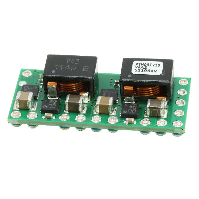
PTH08T210W
SLTS262J – OCTOBER 2005 – REVISED JUNE 2017
PTH08T210W 30-A, 5.5-V to 14-V Input, Non-isolated, Wide Output Adjust,
Power Module withTurboTrans™ Technology
1 Features
•
•
•
•
•
•
•
•
•
1
•
•
•
•
•
•
•
Output Current: Up to 30-A
Input Voltage: 5.5-V to 14-V
Wide-Output Voltage Adjust :0.7 V to 3.6 V
Efficiencies: Up to 96%
Total Output Voltage Variation: ±1.5%
On and Off Inhibit
Differential Output Voltage
Adjustable Undervoltage Lockout
Output Overcurrent Protection
(Nonlatching, Auto-Reset)
Operating Temperature: –40°C to 85°C
POLA™ Compatible
TurboTrans™ Technology
Designed to meet Ultra-Fast Transient
Requirements up to 300 A/μs
Auto-Track™ Sequencing
Multi-Phase, Switch-Mode Topology
Safety Agency Approvals:
– UL/IEC/CSA-22.2 60950-1
2 Applications
•
•
•
Complex Multi-Voltage Systems
Microprocessors
Bus Drivers
3 Description
The PTH08T210W is a high-performance 30-A rated,
non-isolated power module which utilizes a multiphase,
switch-mode
topology.
This
module
represents the 2nd generation of the PTH series
power modules which include a reduced footprint and
improved features.
Operating from an input voltage range of 5.5 V to 14
V, the PTH08T210W requires a single resistor to set
the output voltage to any value over the range, 0.7 V
to 3.6 V. The wide input voltage range makes the
PTH08T210W particularly suitable for advanced
computing and server applications that uses a loosely
regulated 8-V to 12-V intermediate distribution bus.
The module uses double-sided surface mount
construction to provide a low profile and compact
footprint. Package options include both through-hole
and surface mount configurations that are lead (Pb) –
free and RoHS compatible.
A new feature included in this 2nd generation of PTH
and PTV modules is TurboTrans™ technology
(patent pending). TurboTrans technology allows the
transient response of the regulator to be optimized
externally, resulting in a reduction of output voltage
deviation following a load transient and a reduction in
required output capacitance. This feature also offers
enhanced stability when used with ultra-low ESR
output capacitors.
The PTH08T210W incorporates a comprehensive list
of standard features. They include on/off inhibit, a
differential remote output voltage sense which
ensures tight load regulation, and an output
overcurrent and overtemperature shutdown to protect
against load faults. A programmable undervoltage
lockout allows the turn-on voltage threshold to be
customized. AutoTrack™ sequencing is a feature
which simplifies the simultaneous power-up and
power-down of multiple modules in a power system
by allowing the outputs to track a common voltage.
Device Information(1)
PART NUMBER
PTH08T210W
PACKAGE
ECP
BODY SIZE (NOM)
34.8 mm × 18.75 mm
(1) For all available packages, see the orderable addendum at
the end of the data sheet.
1
An IMPORTANT NOTICE at the end of this data sheet addresses availability, warranty, changes, use in safety-critical applications,
intellectual property matters and other important disclaimers. PRODUCTION DATA.
�PTH08T210W
SLTS262J – OCTOBER 2005 – REVISED JUNE 2017
www.ti.com
Simplified Application
Track
TurboTranst
13
14
VI
2,6
Track
TT
+Sense
VI
PTH08T210W
Inhibit
1
3,4
CI
470 µF
(Required)
VO
−Sense
GND
+
RUVLO
1%
0.05 W
(Opional)
5, 9
+Sense
11
INH/UVLO
GND
VO
10
RTT
1%
0.05 W
(Optional)
7,8
VOAdj
12
RSET
1%
0.05 W
(Required)
+
L
O
A
D
CO
470 µF
(Required)
−Sense
GND
GND
UDG−05097
RSET is required to set the output voltage higher than 0.7 V. See the Electrical Characteristics table.
2
Submit Documentation Feedback
Copyright © 2005–2017, Texas Instruments Incorporated
Product Folder Links: PTH08T210W
�PTH08T210W
www.ti.com
SLTS262J – OCTOBER 2005 – REVISED JUNE 2017
Table of Contents
1
2
3
4
5
6
7
Features ..................................................................
Applications ...........................................................
Description .............................................................
Revision History.....................................................
Pin Configuration and Functions .........................
Specifications.........................................................
1
1
1
3
4
5
6.1
6.2
6.3
6.4
6.5
5
5
6
8
9
Absolute Maximum Ratings ......................................
Recommended Operating Conditions.......................
Electrical Characteristics...........................................
Typical Characteristics ..............................................
Typical Characteristics ..............................................
Detailed Description ............................................ 10
7.1 Overview: TurboTrans™ Technology ..................... 10
7.2 Feature Description................................................. 10
8
Application and Implementation ........................ 12
8.1 Application Information............................................ 12
8.2 Typical Application ................................................. 12
9
Device and Documentation Support.................. 28
9.1
9.2
9.3
9.4
9.5
Receiving Notification of Documentation Updates.. 28
Community Resources............................................ 28
Trademarks ............................................................. 28
Electrostatic Discharge Caution .............................. 28
Glossary .................................................................. 28
10 Mechanical, Packaging, and Orderable
Information ........................................................... 29
10.1 Tape and Reel and Tray Drawings ....................... 29
4 Revision History
NOTE: Page numbers for previous revisions may differ from page numbers in the current version.
Changes from Revision I (March 2009) to Revision J
•
Page
Changed typical overcurrent protection threshold (ILIM) from "55 A" to "50 A" in Electrical Characteristics table ................. 6
Submit Documentation Feedback
Copyright © 2005–2017, Texas Instruments Incorporated
Product Folder Links: PTH08T210W
3
�PTH08T210W
SLTS262J – OCTOBER 2005 – REVISED JUNE 2017
www.ti.com
5 Pin Configuration and Functions
PTH08T210W
(TOP VIEW)
1
14
13
12
11
2
3
4
5
6
7
8
9
10
Table 1. Pin Functions
PIN
DESCRIPTION
NAME
NO.
VI
2, 6
The positive input voltage power node to the module, which is referenced to common GND.
VO
5, 9
The regulated positive power output with respect to the GND.
GND
3, 4
7, 8
This is the common ground connection for the VI and VO power connections. It is also the 0 Vdc reference for the
control inputs.
1
The Inhibit pin is an open-collector/drain, negative logic input that is referenced to GND. Applying a low level
ground signal to this input disables the module’s output and turns off the output voltage. When the Inhibit control
is active, the input current drawn by the regulator is significantly reduced. If the Inhibit pin is left open-circuit, the
module produces an output whenever a valid input source is applied. This input is not compatible with TTL logic
devices and should not be tied to VI or any other voltage.
Inhibit (1)/
UVLO adjust
This pin is also used for input undervoltage lockout (UVLO) programming. Connecting a resistor from this pin to
GND (pin 3) allows the ON threshold of the UVLO to be adjusted higher than the default value. For more
information, see the Application Information section.
Vo Adjust
12
A 0.1 W 1% resistor must be directly connected between this pin and pin 8 (GND) to set the output voltage to a
value higher than 0.7 V. The temperature stability of the resistor should be 100 ppm/°C (or better). The setpoint
range for the output voltage is from 0.7 V to 3.6 V. If left open circuit, the output voltage will default to its lowest
value. For further information, on output voltage adjustment see the related application note. The specification
table gives the preferred resistor values for a number of standard output voltages.
+ Sense
10
The sense input allows the regulation circuit to compensate for voltage drop between the module and the load.
For optimal voltage accuracy, +Sense must be connected to VO , very close to the load.
– Sense
11
The sense input allows the regulation circuit to compensate for voltage drop between the module and the load.
For optimal voltage accuracy, –Sense must be connected to GND (pin 8), very close to the load.
Track
14
This is an analog control input that enables the output voltage to follow an external voltage. This pin becomes
active typically 20 ms after the input voltage has been applied, and allows direct control of the output voltage
from 0 V up to the nominal set-point voltage. Within this range the module's output voltage follows the voltage at
the Track pin on a volt-for-volt basis. When the control voltage is raised above this range, the module regulates
at its set-point voltage. The feature allows the output voltage to rise simultaneously with other modules powered
from the same input bus. If unused, this input should be connected to VI.
NOTE: Due to the undervoltage lockout feature, the output of the module cannot follow its own input voltage
during power up. For more information, see the related application note.
TurboTrans™
(1)
4
13
This input pin adjusts the transient response of the regulator. To activate the TurboTrans™ technology feature, a
1%, 50 mW resistor must be connected between this pin and pin 10 (+Sense) very close to the module. For a
given value of output capacitance, a reduction in peak output voltage deviation is achieved by using this feature.
If unused, this pin must be left open-circuit. External capacitance must never be connected to this pin. The
resistance requirement can be selected from the TurboTrans™ resistor table in the Application Information
section.
Denotes negative logic: Open = Normal operation, Ground = Function active
Submit Documentation Feedback
Copyright © 2005–2017, Texas Instruments Incorporated
Product Folder Links: PTH08T210W
�PTH08T210W
www.ti.com
SLTS262J – OCTOBER 2005 – REVISED JUNE 2017
6 Specifications
6.1 Absolute Maximum Ratings
over operating free-air temperature range (unless otherwise noted) (1)
MIN
MAX
UNIT
–0.3
VI + 0.3
V
–40
85
Signal input voltage
Track control (pin 14)
Operating temperature range
Over VI range
PTH08T210WAD
Twave
Wave soldering temperature
Surface temperature of module
body or pins
(5 second maximum)
Treflow
Solder reflow temperature
Surface temperature of module
body or pins
PTH08T210WAS
235 (2)
PTH08T210WAZ
260 (2)
Tstg
Storage temperature
Storage temperature of module removed from shipping
package
Tpkg
Packaging temperature
Shipping Tray or Tape and Reel storage or bake
temperature
45
Mechanical shock
Per Mil-STD-883D, Method 2002.3 1 msec, ½ sine,
mounted
250
Mechanical vibration
Mil-STD-883D, Method 2007.2 20-2000 Hz
15
TA
260
PTH08T210WAH
–55
Weight
(1)
(2)
125
8.5
Flammability
°C
G
grams
Meets UL94V-O
Stresses beyond those listed under Absolute Maximum Ratings may cause permanent damage to the device. These are stress ratings
only, which do not imply functional operation of the device at these or any other conditions beyond those indicated under Recommended
Operating Conditions. Exposure to absolute-maximum-rated conditions for extended periods may affect device reliability.
During reflow of surface mount package version do not elevate peak temperature of the module, pins or internal components above the
stated maximum.
6.2 Recommended Operating Conditions
over operating free-air temperature range (unless otherwise noted)
MIN
NOM
MAX
UNIT
Input Voltage
VI
5.5
14
V
Output Voltage
VO
0.7
3.6
V
Output Current
IO
0
30
A
Operating Ambient Temperature
TA
–40
85
°C
Submit Documentation Feedback
Copyright © 2005–2017, Texas Instruments Incorporated
Product Folder Links: PTH08T210W
5
�PTH08T210W
SLTS262J – OCTOBER 2005 – REVISED JUNE 2017
www.ti.com
6.3 Electrical Characteristics
TA =25°C, VI = 12 V, VO = 3.3 V, CI = 470 µF, CO = 470 µF OS-CON, and IO = IO max (unless otherwise stated)
PARAMETER
TEST CONDITIONS
MIN
TYP
MAX
25°C, natural convection
0
25
60°C, 200 LFM
0
30
UNIT
IO
Output current
VI
Input voltage range
Over IO range
5.5
14
V
Output adjust range
Over IO range
0.7
3.6
V
Set-point voltage
tolerance
VO
ILIM
–40°C < TA < 85°C
±0.3
%Vo
Over VI range
±4
mV
Load regulation
Over IO range
±7
Total output variation
Includes set-point, line, load, –40°C ≤ TA ≤ 85°C
IO = 26 A
VO Ripple (peak-topeak)
20-MHz bandwidth
Overcurrent threshold
Reset, followed by auto-recovery
ttr
Transient response
2.5 A/µs load
step
50 to 100%
IOmax
ttrTT
ΔVtrTT
IIL
Track input current (pin
14)
Pin to GND
dVtrack/dt
Track slew rate
capability
CO ≤ CO (max)
UVLOADJ
Adjustable
Undervoltage lockout
(pin 1)
Pin 1 open
93%
RSET = 5.23 kΩ, VO = 2.5 V
91%
RSET = 12.7 kΩ, VO = 1.8 V
89%
RSET = 19.6 kΩ, VO = 1.5 V
89%
RSET = 35.7 kΩ, VO = 1.2 V
87%
RSET = 63.4 kΩ, VO = 1.0 V
84%
Open, VO = 0.7 V
80%
A
50
µs
VO over/undershoot
150
mV
Recovery time
50
µs
w/o TurboTrans
CO = 940 μF, Type C
VO over/undershoot
125
mV
w/ TurboTrans
CO = 940 μF, Type C
Recovery time
50
µs
VO over/undershoot
85
mV
–130 (2)
1
VI increasing
5
VI decreasing
4.1
Input low voltage (VIL)
Inhibit (pin 1) to GND, Track (pin 14) open
fs
Switching frequency
Over VI and IO ranges
CI
External input
capacitance
6
470
(4)
µA
V/ms
5.5
V
Open (3)
–0.2
Input low current (IIL)
(4)
mVPP
50
Input standby current
(3)
%Vo
Recovery time
Iin
(2)
(1)
25
Input high voltage (VIH)
Inhibit control (pin 1)
mV
±1.5
RSET = 1.62 kΩ, VO = 3.3 V
w/o TurboTrans
CO = 470 μF
ΔVtr
(1)
%Vo
Line regulation
ttr
ΔVtr
(1)
Temperature variation
Efficiency
η
±1
A
0.6
V
125
µA
3
mA
480
kHz
µF
The set-point voltage tolerance is affected by the tolerance and stability of RSET. The stated limit is unconditionally met if RSET has a
tolerance of 1% with 100 ppm/°C or better temperature stability.
A low-leakage (1690 mA
16 × 15
No
TurboTrans
TurboTrans
(Cap
Type) (2)
1
≥ 2 (3)
N/R (4)
EEUFC1E102S
(3)
N/R (4)
EEUFC1E182
Vendor Part No.
FC (Radial)
25 V
1800
0.029Ω
2205 mA
16 × 20
1
≥1
FC(SMD)
25 V
2200
0.028Ω
>2490 mA
18 × 21,5
1
≥ 1 (3)
N/R (4)
EEVFC1E222N
FK(SMD)
25 V
1000
0.060Ω
1100 mA
12,5×13,5
1
≥ 2 (5)
N/R (4)
EEVFK1V102Q
6.3 V
470
0.025Ω
2600 mA
7,3x4,3x2.8
N/R (6)
2 - 4 (3)
C ≥ 2 (2)
United Chemi-Con
PTB, Poly-Tantalum(SMD)
N/R (4)
6PTB477MD8TER
LXZ, Aluminum (Radial)
25 V
680
0.068Ω
1050 mA
10 × 16
1
PS, Poly-Alum(Radial)
16 V
330
0.014Ω
5060 mA
10 × 12,5
2
2-3
B ≥ 2 (2)
16PS330MJ12
PXA, Poly-Alum(SMD)
16 V
330
0.014Ω
5050 mA
10 × 12,2
2
2-3
B ≥ 2 (2)
PXA16VC331MJ12TP
PS, Poly-Alum(Radial)
6.3 V
680
0.010Ω
5500 mA
10 × 12,5
N/R (6)
1-2
C ≥ 1 (2)
6PS680MJ12
PXA, Poly-Alum(Radial)
6.3 V
470
0.012Ω
4770 mA
8 × 12,2
N/R (6)
1-2
C ≥ 1 (2)
PXA6.3VC471MH12TP
Nichicon, Aluminum
25 V
470
0.070Ω
985 mA
12,5 × 15
1
≥ 2 (3)
N/R (4)
UPM1E471MHH6
HD (Radial)
25 V
470
0.038Ω
1430 mA
10 × 16
1
≥ 2 (3)
N/R (4)
UHD1E471MHR
PM (Radial)
35 V
560
0.048Ω
1360 mA
16 × 15
1
≥ 2 (3)
N/R (4)
UPM1V561MHH6
Panasonic, Poly-Alum
N/R
1-3
(3)
(6)
N/R
(6)
B≥2
LXZ25VB681M10X20LL
(2)
EEFSE0J391R(VO≤1.6V) (7)
2.0 V
390
0.005Ω
4000 mA
7,3×4,3×4,2
6.3 V
470
0.018Ω
3500 mA
7,3 × 4,3
N/R (6)
1-3
C ≥ 1 (2)
6TPE470MI
7,3 × 4,3
N/R
(6)
1-2
B ≥ 2 (2)
2R5TPE470M7(VO ≤ 1.8 V) (7)
N/R
(6)
Sanyo
TPE, Poscap (SMD)
TPE Poscap(SMD)
TPD Poscap (SMD)
2.5 V
2.5 V
470
1000
0.007Ω
0.005Ω
4400 mA
6100 mA
7,3 × 4,3
1
B≥1
(4)
2R5TPD1000M5(VO ≤ 1.8 V) (7)
SA, Os-Con (Radial)
16 V
470
0.020Ω
>6080 mA
16 × 23
1
1-4
SP Oscon ( Radial)
10 V
470
0.015
>4500 mA
10 × 11,5
N/R (6)
1-3
C ≥ 2 (2)
10SP470M
SEPC, Os-Con (Radial)
16 V
470
0.010Ω
>4700 mA
10 × 13
1
1-2
B ≥ 1 (2)
16SEPC470M
SVPA, Os-Con (SMD)
6.3 V
470
0.020Ω
4700mA
10 × 10,3
N/R (6)
1 - 4 (3)
(1)
(2)
(3)
(4)
(5)
(6)
(7)
N/R
(2)
C ≥ 1 (2)
16SA470M
(3)
6SVPA470M
Capacitor Supplier Verification
Please verify availability of capacitors identified in this table. Capacitor suppliers may recommend alternative part numbers because of
limited availability or obsolete products. In some instances, the capacitor product life cycle may be in decline and have short-term
consideration for obsolescence.
RoHS, Lead-free and Material Details
See the capacitor suppliers regarding material composition, RoHS status, lead-free status, and manufacturing process requirements.
Component designators or part number deviations can occur when material composition or soldering requirements are updated.
Required capacitors with TurboTrans. See the TransTrans Application information for Capacitor Selection
Capacitor Type Groups by ESR (Equivalent Series Resistance) :
(a) Type A = (100 < capacitance × ESR ≤ 1000)
(b) Type B = (1,000 < capacitance × ESR ≤ 5,000)
(c) Type C = (5,001 < capacitance × ESR ≤ 10,000)
Total bulk nonceramic capacitors on the output bus with ESR of ≥ 15mΩ to ≤ 30mΩ requires an additional ≥ 200 μF of ceramic
capacitor.
Aluminum Electrolytic capacitor not recommended for the TurboTrans due to higher ESR × capacitance products. Aluminum and higher
ESR capacitors can be used in conjunction with lower ESR capacitance.
Output bulk capacitor's maximum ESR is ≥ 30 mΩ. Additional ceramic capacitance of ≥ 200 μF is required.
N/R – Not recommended. The voltage rating does not meet the minimum operating limits.
The voltage rating of this capacitor only allows it to be used for output voltage that is equal to or less than 80% of the working voltage.
Submit Documentation Feedback
Copyright © 2005–2017, Texas Instruments Incorporated
Product Folder Links: PTH08T210W
15
�PTH08T210W
SLTS262J – OCTOBER 2005 – REVISED JUNE 2017
www.ti.com
Typical Application (continued)
Table 2. Input/Output Capacitors(1) (continued)
Capacitor Characteristics
Capacitor Vendor,
Type Series (Style)
AVX, Tantalum, Series III
TPM Multianode
Working Value
Voltage
(µF)
6.3 V
680
Quantity
Max.
ESR
at 100
kHz
Max
Ripple
Current at
85°C
(Irms)
Physical
Size (mm)
Input
Bus
Output Bus
0.035Ω
>2400 mA
7,3×4,3×4,1
No
TurboTrans
TurboTrans
(Cap
Type) (2)
N/R (6)
2 - 7 (3)
N/R (4)
(6)
(3)
N/R
2-3
C ≥ 2 (2)
Vendor Part No.
TPSE477M010R0045
(3)
6.3 V
470
0.018Ω
>3800 mA
7,3×4,3×4,1
TPS Series III (SMD)
4V
1000
0.035Ω
2405 mA
7,3 × 5,7
N/R (6)
2 - 7 (3)
N/R (4)
TPME687M006#0018
Kemet, Poly-Tantalum
6.3 V
470
0.018Ω
2700 mA
7,3×4.3×4
N/R (6)
1 - 3 (3)
C ≥ 2 (2)
T520X477M06ASE018
(6)
1-2
B ≥ 1 (2)
T530X477M006ASE010
TPSV108K004R0035
(VO ≤ 2.2 V) (7)
T520 (SMD)
6.3 V
470
0.010Ω
>5200 mA
7,3×4.3×4
N/R
T530 (SMD)
6.3 V
470
0.005Ω
7300 mA
7,3×4.3×4
N/R (6)
1
B ≥ 1 (2)
T530X477M006ASE005
T530 (SMD)
2.5 V
1000
0.005Ω
7300 mA
7,3×4.3×4
N/R (6)
1
B ≥ 1 (2)
T530X108M2R5ASE005
(VO ≤ 2.0 V) (7)
594D, Tantalum (SMD)
6.3 V
1000
0.030Ω
2890 mA
7,2×5,7×4,1
N/R (6)
1-6
N/R (4)
594D108X06R3R2TR2T
94SA, Os-con (Radial)
16 V
1000
0.015Ω
9740 mA
16 × 25
1
1-3
N/R (4)
94SA108X0016HBP
94SVP Os-Con(SMD)
16 V
330
0.017Ω
>4500 mA
10 × 12,7
2
2-3
C ≥ 1 (2)
94SVP827X06R3F12
Kemet, Ceramic X5R
16 V
10
0.002Ω
–
3225
1
≥ 1 (8)
A (2)
C1210C106M4PAC
(SMD)
6.3 V
47
0.002Ω
N/R (6)
≥ 1 (8)
A (2)
C1210C476K9PAC
Murata, Ceramic X5R
6.3 V
100
0.002Ω
N/R (6)
≥ 1 (8)
A (2)
GRM32ER60J107M
(SMD)
6.3 V
47
N/R (6)
≥ 1 (8)
A (2)
GRM32ER60J476M
(8)
(2)
GRM32ER61E226K
Vishay-Sprague
–
3225
25 V
22
1
≥1
16 V
10
1
≥ 1 (8)
A (2)
GRM32DR61C106K
TDK, Ceramic X5R
6.3 V
100
N/R (6)
≥ 1 (8)
A (2)
C3225X5R0J107MT
(SMD)
6.3 V
47
N/R (6)
≥ 1 (8)
A (2)
C3225X5R0J476MT
16 V
10
1
≥ 1 (8)
A (2)
C3225X5R1C106MT0
16 V
22
1
≥ 1 (8)
A (2)
C3225X5R1C226MT
(8)
0.002Ω
–
3225
A
Maximum ceramic capacitance on the output bus is ≤ 3000 μF. Any combination of the ceramic capacitor values is limited to 3000 μF for
non-TurboTrans applications. The total capacitance is limited to 14,000 μF which includes all ceramic and non-ceramic types.
8.2.1.2 TurboTrans™ Selection
Utilizing TurboTrans requires connecting a resistor, RTT, between the +Sense pin (pin 10) and the TurboTrans
pin (pin 13). The value of the resistor directly corresponds to the amount of output capacitance required. All T2
products require a minimum value of output capacitance whether or not TurboTrans is used. For the
PTH08T210W, the minimum required capacitance is 470 μF. When using TurboTrans, capacitors with a
capacitance × ESR product below 10,000 μF × mΩ are required. (Multiply the capacitance (in μF) by the ESR (in
mΩ) to determine the capacitance × ESR product.) See the Capacitor Selection section of the datasheet for a
variety of capacitors that meet this criteria.
Figure 14 through Figure 19, show the amount of output capacitance required to meet a desired transient voltage
deviation with and without TurboTrans for several capacitor types; Type A (e.g. ceramic), Type B (e.g. polymertantalum), and Type C (e.g. OS-CON). To calculate the proper value of RTT, first determine the required transient
voltage deviation limits and magnitude of the transient load step. Next, determine what type of output capacitors
to be used. (If more than one type of output capacitor is used, select the capacitor type that makes up the
majority of the total output capacitance.) Knowing this information, use the chart in Figure 14 through Figure 19
that corresponds to the capacitor type selected. To use the chart, begin by dividing the maximum voltage
deviation limit (in mV) by the magnitude of the load step (in Amps). This gives a mV/A value. Find this value on
the Y-axis of the appropriate chart. Read across the graph to the 'With TurboTrans' plot. From this point, read
down to the X-axis which lists the minimum required capacitance, CO, to meet the transient voltage deviation.
The required RTT resistor value can then be calculated using Equation 1 or selected from the TurboTrans table.
The TurboTrans tables include both the required output capacitance and the corresponding RTT values to meet
several values of transient voltage deviation for 25% (7.5 A), 50% (15 A), and 75% (22.5 A) output load steps.
16
Submit Documentation Feedback
Copyright © 2005–2017, Texas Instruments Incorporated
Product Folder Links: PTH08T210W
�PTH08T210W
www.ti.com
SLTS262J – OCTOBER 2005 – REVISED JUNE 2017
The chart can also be used to determine the achievable transient voltage deviation for a given amount of output
capacitance. Selecting the amount of output capacitance along the X-axis, reading up to the 'With TurboTrans'
curve, and then over to the Y-axis, gives the transient voltage deviation limit for that value of output capacitance.
The required RTT resistor value can be calculated using Equation 1 or selected from the TurboTrans table.
As an example, let's look at a 12-V application requiring a 75 mV deviation during a 15 A, 50% load transient. A
majority of 330 μF, 10 mΩ output capacitors will be used. Use the 12 V, Type B capacitor chart, Figure 16.
Dividing 75 mV by 15 A gives 5 mV/A transient voltage deviation per amp of transient load step. Select 5 mV/A
on the Y-axis and read across to the 'With TurboTrans' plot. Following this point down to the X-axis gives us a
minimum required output capacitance of approximately 1300 μF. The required RTT resistor value for 1300 μF can
then be calculated or selected from Figure 16. The required RTT resistor is approximately 10.2 kΩ.
To see the benefit of TurboTrans, follow the 5 mV/A marking across to the 'Without TurboTrans' plot. Following
that point down shows that a minimum of 8200 μF of output capacitance is required to meet the same transient
deviation limit. This is the benefit of TurboTrans. A typical TurboTrans application schematic is shown in
Figure 13.
20
20
Without Turbo Trans
10
9
8
7
6
5
Transient - mV/A
With Turbo Trans
4
3
10
9
8
7
6
5
With Turbo Trans
4
3
2
2
VI = 8 V
VI = 12 V
4000
5000
6000
7000
8000
9000
10000
3000
2000
400
4000
5000
6000
7000
8000
9000
10000
3000
2000
400
1
500
600
700
800
900
1000
1
500
600
700
800
900
1000
Transient - mV/A
Without Turbo Trans
C - Capacitance - mF
100 ≤ C(μF) × ESR (mΩ) ≤ 1000
12-V Input
C - Capacitance - mF
100 ≤ C(μF) × ESR (mΩ) ≤ 1000
8-V Input
Figure 14. Type A Capacitor (Ceramic)
Figure 15. Type A Capacitor (Ceramic)
Table 3. Type A TurboTrans CO Values and Required RTT Selection Table
Transient Voltage Deviation (mV)
12 V Input
25%
Load Step
(7.5 A)
50%
Load Step
(15 A)
75%
Load Step
(22.5 A)
CO
Minimum Required
Output
Capacitance
(μF)
130
260
390
120
240
360
110
220
100
90
8 V Input
RTT
Required
TurboTrans
Resistor (Ω)
CO
Minimum Required
Output
Capacitance
(μF)
RTT
Required
TurboTrans
Resistor (Ω)
470
open
580
127 k
520
294 k
640
80.6 k
330
580
127 k
710
54.9 k
200
300
650
76.8 k
800
37.4 k
180
270
740
47.5 k
900
26.7 k
80
160
240
850
31.6 k
1050
17.8 k
70
140
210
1000
20.5 k
1250
11.3 k
60
120
180
1200
12.7 k
1500
6.65 k
50
100
150
1500
6.65 k
1900
2.55 k
Submit Documentation Feedback
Copyright © 2005–2017, Texas Instruments Incorporated
Product Folder Links: PTH08T210W
17
�PTH08T210W
SLTS262J – OCTOBER 2005 – REVISED JUNE 2017
www.ti.com
Table 3. Type A TurboTrans CO Values and Required RTT Selection Table (continued)
Transient Voltage Deviation (mV)
12 V Input
8 V Input
25%
Load Step
(7.5 A)
50%
Load Step
(15 A)
75%
Load Step
(22.5 A)
CO
Minimum Required
Output
Capacitance
(μF)
RTT
Required
TurboTrans
Resistor (Ω)
CO
Minimum Required
Output
Capacitance
(μF)
RTT
Required
TurboTrans
Resistor (Ω)
40
80
120
2000
1.82 k
2600
0
30
60
90
4000
0
7800
0
8.2.1.2.1 RTT Resistor Selection
The TurboTrans resistor value, RTT can be determined from the TurboTrans programming equation, see
Equation 1.
1 - (CO / 2350)
kW
RTT = 40 ´
5 x (CO / 2350) - 1
(1)
Where CO is the total output capacitance in μF. CO values greater than or equal to 2350 μF require RTT to be a
short, 0Ω. (Equation 1 will result in a negative value for RTT when CO ≥ 2350 μF.)
20
20
Without Turbo Trans
Transient - mV/A
7
6
5
With Turbo Trans
4
3
10
9
8
7
6
5
With Turbo Trans
4
3
C - Capacitance - mF
1000 ≤ C(μF)xESR(mΩ) ≤ 5000
12-V Input
4000
5000
6000
7000
8000
9000
10000
3000
2000
2
400
4000
5000
6000
7000
8000
9000
10000
3000
2000
400
2
VI = 12 V
500
600
700
800
900
1000
VI = 12 V
500
600
700
800
900
1000
Transient - mV/A
Without Turbo Trans
10
9
8
C - Capacitance - mF
1000 ≤ C(μF)xESR(mΩ) ≤ 5000
12-V Input
Figure 16. Type B Capacitor (e.g. Polymer-Tantalum)
Figure 17. Type B Capacitor (e.g. Polymer-Tantalum)
Table 4. Type B TurboTrans COValues and Required RTT Selection Table
Transient Voltage Deviation (mV)
12 V Input
25%
Load Step
(7.5 A)
50%
Load Step
(15 A)
75%
Load Step
(22.5 A)
CO
Minimum Required
Output Capacitance
(μF)
100
200
300
90
180
270
80
160
70
60
50
18
8 V Input
RTT
Required
TurboTrans
Resistor (Ω)
CO
Minimum Required
Output Capacitance
(μF)
470
open
540
205 k
500
499 k
620
93.1 k
240
580
127 k
720
52.3 k
140
210
680
63.4 k
840
32.4 k
120
180
800
37.4 k
1000
20.5 k
100
150
1000
20.5 k
1300
10.2 k
Submit Documentation Feedback
RTT
Required
TurboTrans
Resistor (Ω)
Copyright © 2005–2017, Texas Instruments Incorporated
Product Folder Links: PTH08T210W
�PTH08T210W
www.ti.com
SLTS262J – OCTOBER 2005 – REVISED JUNE 2017
Table 4. Type B TurboTrans COValues and Required RTT Selection Table (continued)
Transient Voltage Deviation (mV)
12 V Input
8 V Input
25%
Load Step
(7.5 A)
50%
Load Step
(15 A)
75%
Load Step
(22.5 A)
CO
Minimum Required
Output Capacitance
(μF)
RTT
Required
TurboTrans
Resistor (Ω)
CO
Minimum Required
Output Capacitance
(μF)
RTT
Required
TurboTrans
Resistor (Ω)
40
80
120
1300
10.2 k
1700
4.22 k
30
60
90
1800
3.32 k
2300
221
25
50
75
2200
698
4900
0
20
40
60
5400
0
14000
0
8.2.1.2.2 RTT Resistor Selection
The TurboTrans resistor value, RTT can be determined from the TurboTrans programming equation, see
Equation 1.
CO values greater than or equal to 2350 μF require RTT to be a short, 0Ω. (Equation 1 will result in a negative
value for RTT when CO ≥ 2350 μF.)
20
10
9
8
Without Turbo Trans
Transient - mV/A
7
6
5
With Turbo Trans
4
10
9
8
Without Turbo Trans
7
6
5
With Turbo Trans
4
3
3
C - Capacitance - mF
5000 ≤ C(μF) × ESR(mΩ) ≤
12-V Input
10,000
4000
5000
6000
7000
8000
9000
10000
3000
2000
400
4000
2
5000
6000
7000
8000
9000
10000
2000
3000
VI = 8 V
500
600
700
800
900
1000
2
400
VI = 12 V
500
600
700
800
900
1000
Transient - mV/A
20
C - Capacitance - mF
5000 ≤ C(μF) × ESR(mΩ) ≤
8-V Input
10,000
Figure 18. Type C Capacitor
Figure 19. Type C Capacitor
Table 5. Type C TurboTrans COValues and Required RTT Selection Table
Transient Voltage Deviation (mV)
25%
50%
75%
Load Step Load Step Load Step
(7.5 A)
(15 A)
(22.5 A)
12 V Input
CO
Minimum Required
Output Capacitance
(μF)
8 V Input
RTT
Required TurboTrans
Resistor (Ω)
CO
Minimum Required
Output Capacitance
(μF)
RTT
Required TurboTrans
Resistor (Ω)
80
160
240
470
open
520
294 k
70
140
210
560
158 k
620
93.1 k
60
120
180
680
63.4 k
750
45.3 k
50
100
150
850
31.6 k
940
24.3 k
40
80
120
1100
15.8 k
1300
10.2 k
35
70
105
1300
10.2 k
1500
6.65 k
Submit Documentation Feedback
Copyright © 2005–2017, Texas Instruments Incorporated
Product Folder Links: PTH08T210W
19
�PTH08T210W
SLTS262J – OCTOBER 2005 – REVISED JUNE 2017
www.ti.com
Table 5. Type C TurboTrans COValues and Required RTT Selection Table (continued)
Transient Voltage Deviation (mV)
25%
50%
75%
Load Step Load Step Load Step
(7.5 A)
(15 A)
(22.5 A)
12 V Input
8 V Input
CO
Minimum Required
Output Capacitance
(μF)
RTT
Required TurboTrans
Resistor (Ω)
CO
Minimum Required
Output Capacitance
(μF)
RTT
Required TurboTrans
Resistor (Ω)
30
60
90
1600
5.36 k
1800
3.32 k
25
50
75
2000
1.82 k
2200
698
20
40
60
4000
0
5400
0
8.2.1.2.3 RTT Resistor Selection
The TurboTrans resistor value, RTT can be determined from the TurboTrans programming equation, see
Equation 1.
CO values greater than or equal to 2350 μF require RTT to be a short, 0Ω. (Equation 1 will result in a negative
value for RTT when CO ≥ 2350 μF.)
8.2.1.3 Adjusting the Output Voltage
The VO Adjust control (pin 12) sets the output voltage of the PTH08T210W. The adjustment range of the
PTH08T210W is 0.7 V to 3.6 V. The adjustment method requires the addition of a single external resistor, RSET,
that must be connected directly between the Vo Adjust and GND pins. Table 6 gives the preferred value of the
external resistor for a number of standard voltages, along with the actual output voltage that this resistance value
provides.
For other output voltages, the value of the required resistor can either be calculated using the following formula,
or simply selected from the range of values given in Table 7. Figure 20 shows the placement of the required
resistor.
0.7
R
+ 30.1 kW
* 6.49 kW
SET
V * 0.7
O
(2)
Table 6. Preferred Values of RSET for Standard Output Voltages
20
VO (Standard) (V)
RSET (Preferred Value) (Ω)
VO (Actual) (V)
3.3
1.62 k
3.298
2.5
5.23 k
2.498
2
9.76 k
1.997
1.8
12.7 k
1.798
1.5
19.6 k
1.508
1.2
35.7 k
1.199
1
63.4 k
1.001
0.7
Open
0.700
Submit Documentation Feedback
Copyright © 2005–2017, Texas Instruments Incorporated
Product Folder Links: PTH08T210W
�PTH08T210W
www.ti.com
SLTS262J – OCTOBER 2005 – REVISED JUNE 2017
+Sense
+Sense
10
9
PTH08T210W
−Sense
GND
GND
3 4
7
8
VO
5
VO
11
VOAdj
12
CO
RSET
1%
0.05 W
−Sense
GND
(1)
Use a 0.05 W resistor. The tolerance should be 1%, with temperature stability of 100 ppm/°C (or better). Place the
resistor as close to the regulator as possible. Connect the resistor directly between pins 12 and 8 using dedicated
PCB traces.
(2)
Never connect capacitors from VO Adjust to either GND or VO. Any capacitance added to the VO Adjust pin affects the
stability of the regulator.
Figure 20. VO Adjust Resistor Placement
Submit Documentation Feedback
Copyright © 2005–2017, Texas Instruments Incorporated
Product Folder Links: PTH08T210W
21
�PTH08T210W
SLTS262J – OCTOBER 2005 – REVISED JUNE 2017
www.ti.com
Table 7. Output Voltage Set-Point Resistor Values
22
Va Required (V)
RSET (kΩ)
Va Required (V)
RSET (kΩ)
0.70
Open
2.10
8.66
0.75
412
2.20
7.50
0.80
205
2.30
6.65
0.85
133
2.40
5.90
0.90
97.6
2.50
5.23
0.95
78.7
2.60
4.64
1.00
63.4
2.70
4.02
1.10
46.4
2.80
3.57
1.20
35.7
2.90
3.09
1.30
28.7
3.00
2.67
1.40
23.7
3.10
2.26
1.50
19.6
3.20
1.96
1.60
16.9
3.30
1.62
1.70
14.7
3.40
1.30
1.80
12.7
3.50
1.02
1.90
11.0
3.60
0.768
2.00
9.76
Submit Documentation Feedback
Copyright © 2005–2017, Texas Instruments Incorporated
Product Folder Links: PTH08T210W
�PTH08T210W
www.ti.com
SLTS262J – OCTOBER 2005 – REVISED JUNE 2017
8.2.1.4 Undervoltage Lockout (UVLO)
The PTH08T210W power modules incorporate an input undervoltage lockout (UVLO). The UVLO feature
prevents the operation of the module until there is sufficient input voltage to produce a valid output voltage. This
enables the module to provide a clean, monotonic powerup for the load circuit, and also limits the magnitude of
current drawn from the regulator’s input source during the power-up sequence.
The UVLO characteristic is defined by the ON threshold (VTHD) voltage. Below the ON threshold the module does
not produce an output. The Inhibit control becomes active when the input voltage is greater then 4.25 V. The
hysterisis voltage, which is the difference between the ON and OFF threshold voltages, is nominally set at
900 mV. The hysterisis prevents start-up oscillations, which can occur if the input voltage droops slightly when
the module begins drawing current from the input source.
8.2.1.5 UVLO Adjustment
The UVLO feature of the PTH08T210W module allows for limited adjustment of the ON threshold voltage. The
adjustment is made via the Inhbit/UVLO Prog control pin (pin 1). When pin 1 is left open circuit, the ON threshold
voltage is internally set to its default value. The ON threshold has a nominal voltage of 5.0 V, and the hysterisis
900 mV. This ensures that the module produces a regulated output when the minimum input voltage is applied.
The ON threshold might need to be increased if the module is powered from a tightly regulated 12-V bus. This
allows the ON threshold voltage to be set for a specified input voltage. Adjusting the threshold voltage prevents
the module from operating if the input bus fails to completely rise to its specified regulation voltage.
Equation 3 determines the value of RTHD required to adjust VTHD to a new value. The default value is 5 V, and it
may only be adjusted to a higher value.
RUVLO =
2590 - (24.9 x (VI - 1))
24.9 x (VI - 1) - 100
kW
(3)
Table 8 lists the standard resistor values for RUVLO for different options of the on-threshold (VTHD) voltage.
Table 8. Calculated Values of RUVLO for Various Values of VTHD
VTHD
6.5 V
7.0 V
7.5 V
8.0 V
8.5 V
9.0 V
9.5 V
10.0 V
10.5 V
RUVLO
66.5 kΩ
49.9 kΩ
39.2 kΩ
32.4 kΩ
27.4 kΩ
24.3 kΩ
21.5 kΩ
19.1 kΩ
17.4 kΩ
VI
2
VI
1
PTH08T210W
Inhibit/
UVLO Prog
GND
3
CI
4
RUVLO
GND
Figure 21. UVLO Program Resistor Placement
Submit Documentation Feedback
Copyright © 2005–2017, Texas Instruments Incorporated
Product Folder Links: PTH08T210W
23
�PTH08T210W
SLTS262J – OCTOBER 2005 – REVISED JUNE 2017
www.ti.com
8.2.1.6 Output On/Off Inhibit
For applications requiring output voltage on/off control, the PTH08T210W incorporates an output Inhibit control
pin. The inhibit feature can be used wherever there is a requirement for the output voltage from the regulator to
be turned off.
The power modules function normally when the Inhibit pin is left open-circuit, providing a regulated output
whenever a valid source voltage is connected to VI with respect to GND. The Inhibit function becomes active
when the input voltage is greater than 4.25 V.
Figure 22 shows the typical application of the inhibit function. Note the discrete transistor (Q1). The Inhibit input
has its own internal pull-up to a potential of 5 V. The input is not compatible with TTL logic devices and should
not be tied to VI. An open-collector (or open-drain) discrete transistor is recommended for control.
VI
2, 6
VO (2 V/div)
VI
PTH08T210W
II (5 A/div)
1 Inhibit/
UVLO
GND
3,4
CI
1 = Inhibit
7,8
VINH (2 V/div)
Q1
BSS 138
GND
t − Time − 10 ms/div
Figure 22. On/Off Inhibit Control Circuit
Figure 23. Power-Up Response from Inhibit Control
Turning Q1 on applies a low voltage to the Inhibit control pin and disables the output of the module. If Q1 is then
turned off, the module executes a soft-start power-up sequence. A regulated output voltage is produced within 25
ms. Figure 23 shows the typical rise in both the output voltage and input current, following the turn-off of Q1. The
turn off of Q1 corresponds to the rise in the waveform, Q1 VDS. The waveforms were measured with a 20-A
constant current load.
NOTE
When applying a low voltage (≤0.6 V) to the Inhibit control pin to turn off the module, the
low side FET will immediately discharge any capacitance on the output bus. Depending on
the amount and type of capacitors, this may induce a negative voltage transient that can
momentarily go below GND potential. If turn-off control is desired, the Auto-Track pin can
be used to the control ramp up and ramp down of the output voltage.
8.2.1.7 Overcurrent Protection
For protection against load faults, all modules incorporate output overcurrent protection. Applying a load that
exceeds the regulator's overcurrent threshold causes the regulated output to shut down. Following shutdown, a
module periodically attempts to recover by initiating a soft-start power-up. This is described as a hiccup mode of
operation, whereby the module continues in a cycle of successive shutdown and power up until the load fault is
removed. During this period, the average current flowing into the fault is significantly reduced. Once the fault is
removed, the module automatically recovers and returns to normal operation.
24
Submit Documentation Feedback
Copyright © 2005–2017, Texas Instruments Incorporated
Product Folder Links: PTH08T210W
�PTH08T210W
www.ti.com
SLTS262J – OCTOBER 2005 – REVISED JUNE 2017
8.2.1.8 Overtemperature Protection (OTP)
A thermal shutdown mechanism protects the module’s internal circuitry against excessively high temperatures. A
rise in the internal temperature may be the result of a drop in airflow, or a high ambient temperature. If the
internal temperature exceeds the OTP threshold, the module’s Inhibit control is internally pulled low. This turns
the output off. The output voltage drops as the external output capacitors are discharged by the load circuit. The
recovery is automatic, and begins with a soft-start power up. It occurs when the sensed temperature decreases
by about 10°C below the trip point.
The overtemperature protection is a last resort mechanism to prevent thermal stress to the regulator.
Operation at or close to the thermal shutdown temperature is not recommended and reduces the long-term
reliability of the module. Always operate the regulator within the specified safe operating area (SOA) limits for
the worst-case conditions of ambient temperature and airflow.
8.2.1.9 Auto-Track™ Function
The Auto-Track function is unique to the PTH/PTV family, and is available with all POLA products. Auto-Track
was designed to simplify the amount of circuitry required to make the output voltage from each module power up
and power down in sequence. The sequencing of two or more supply voltages during power up is a common
requirement for complex mixed-signal applications that use dual-voltage VLSI ICs such as the TMS320™ DSP
family, microprocessors, and ASICs.
8.2.1.9.1 How Auto-Track™ Works
Auto-Track works by forcing the module output voltage to follow a voltage presented at the Track control pin (1).
This control range is limited to between 0 V and the module set-point voltage. Once the track-pin voltage is
raised above the set-point voltage, the module output remains at its set-point (2). As an example, if the Track pin
of a 2.5-V regulator is at 1 V, the regulated output is 1 V. If the voltage at the Track pin rises to 3 V, the regulated
output does not go higher than 2.5 V.
When under Auto-Track control, the regulated output from the module follows the voltage at its Track pin on a
volt-for-volt basis. By connecting the Track pin of a number of these modules together, the output voltages follow
a common signal during power up and power down. The control signal can be an externally generated master
ramp waveform, or the output voltage from another power supply circuit (3). For convenience, the Track input
incorporates an internal RC-charge circuit. This operates off the module input voltage to produce a suitable rising
waveform at power up.
8.2.1.9.2 Typical Application
The basic implementation of Auto-Track allows for simultaneous voltage sequencing of a number of Auto-Track
compliant modules. Connecting the Track inputs of two or more modules forces their track input to follow the
same collective RC-ramp waveform, and allows their power-up sequence to be coordinated from a common
Track control signal. This can be an open-collector (or open-drain) device, such as a power-up reset voltage
supervisor IC. See U3 in Figure 24.
To coordinate a power-up sequence, the Track control must first be pulled to ground potential. This should be
done at or before input power is applied to the modules. The ground signal should be maintained for at least
20 ms after input power has been applied. This brief period gives the modules time to complete their internal
soft-start initialization (4), enabling them to produce an output voltage. A low-cost supply voltage supervisor IC,
that includes a built-in time delay, is an ideal component for automatically controlling the Track inputs at power
up.
Figure 24 shows how the TL7712A supply voltage supervisor IC (U3) can be used to coordinate the sequenced
power up of PTH08T210W modules. The output of the TL7712A supervisor becomes active above an input
voltage of 3.6 V, enabling it to assert a ground signal to the common track control well before the input voltage
has reached the module's undervoltage lockout threshold. The ground signal is maintained until approximately 28
ms after the input voltage has risen above U3's voltage threshold, which is 10.95 V. The 28-ms time period is
controlled by the capacitor C3. The value of 2.2 µF provides sufficient time delay for the modules to complete
their internal soft-start initialization. The output voltage of each module remains at zero until the track control
voltage is allowed to rise. When U3 removes the ground signal, the track control voltage automatically rises. This
causes the output voltage of each module to rise simultaneously with the other modules, until each reaches its
respective set-point voltage.
Submit Documentation Feedback
Copyright © 2005–2017, Texas Instruments Incorporated
Product Folder Links: PTH08T210W
25
�PTH08T210W
SLTS262J – OCTOBER 2005 – REVISED JUNE 2017
www.ti.com
Figure 25 shows the output voltage waveforms after input voltage is applied to the circuit. The waveforms, VO1
and VO2, represent the output voltages from the two power modules, U1 (3.3 V) and U2 (1.8 V), respectively.
VTRK, VO1, and VO2 are shown rising together to produce the desired simultaneous power-up characteristic.
The same circuit also provides a power-down sequence. When the input voltage falls below U3's voltage
threshold, the ground signal is re-applied to the common track control. This pulls the track inputs to zero volts,
forcing the output of each module to follow, as shown in Figure 26. Power down is normally complete before the
input voltage has fallen below the modules' undervoltage lockout. This is an important constraint. Once the
modules recognize that an input voltage is no longer present, their outputs can no longer follow the voltage
applied at their track input. During a power-down sequence, the fall in the output voltage from the modules is
limited by the Auto-Track slew rate capability.
8.2.1.9.3 Notes on Use of Auto-Track™
1. The Track pin voltage must be allowed to rise above the module set-point voltage before the module
regulates at its adjusted set-point voltage.
2. The Auto-Track function tracks almost any voltage ramp during power up, and is compatible with ramp
speeds of up to 1 V/ms.
3. The absolute maximum voltage that may be applied to the Track pin is the input voltage VI.
4. The module cannot follow a voltage at its track control input until it has completed its soft-start initialization.
This takes about 20 ms from the time that a valid voltage has been applied to its input. During this period, it
is recommended that the Track pin be held at ground potential.
5. The Auto-Track function is disabled by connecting the Track pin to the input voltage (VI). When Auto-Track is
disabled, the output voltage rises at a quicker and more linear rate after input power has been applied.
RTT
U1
AutoTrack TurboTrans
+Sense
VI = 12 V
VI
VO
PTH08T210W
VO1 = 3.3 V
Inhibit/
UVLO Prog
−Sense
VOAdj
GND
+
U3
7
2
1
3
RSET
1.62 kW
8
VCC
SENSE
5
RESET
RESIN
TL7712A
REF
CT
6
AutoTrack TurboTrans
Smart
+Sense
Sync
4
CT
2.2 mF
RTT
U2
RESET
GND
CREF
0.1 mF
CO1
CI1
RRST
10 kW
VI
VO
PTH08T220W
VO 2 = 1.8 V
Inhibit/
UVLO Prog
−Sense
GND
+
VOAdj
CO2
CI2
RSET2
4.75 kW
Figure 24. Sequenced Power Up and Power Down Using Auto-Track
26
Submit Documentation Feedback
Copyright © 2005–2017, Texas Instruments Incorporated
Product Folder Links: PTH08T210W
�PTH08T210W
www.ti.com
SLTS262J – OCTOBER 2005 – REVISED JUNE 2017
VTRK (1 V/div)
VTRK (1 V/div)
VO1 (1 V/div)
VO1 (1 V/div)
VO2 (1 V/div)
VO2 (1 V/div)
t − Time − 20 ms/div
t − Time − 400 ms/div
Figure 25. Simultaneous Power Up
With Auto-Track Control
Figure 26. Simultaneous Power Down
With Auto-Track Control
Submit Documentation Feedback
Copyright © 2005–2017, Texas Instruments Incorporated
Product Folder Links: PTH08T210W
27
�PTH08T210W
SLTS262J – OCTOBER 2005 – REVISED JUNE 2017
www.ti.com
9 Device and Documentation Support
9.1 Receiving Notification of Documentation Updates
To receive notification of documentation updates, navigate to the device product folder on ti.com. In the upper
right corner, click on Alert me to register and receive a weekly digest of any product information that has
changed. For change details, review the revision history included in any revised document.
9.2 Community Resources
The following links connect to TI community resources. Linked contents are provided "AS IS" by the respective
contributors. They do not constitute TI specifications and do not necessarily reflect TI's views; see TI's Terms of
Use.
TI E2E™ Online Community TI's Engineer-to-Engineer (E2E) Community. Created to foster collaboration
among engineers. At e2e.ti.com, you can ask questions, share knowledge, explore ideas and help
solve problems with fellow engineers.
Design Support TI's Design Support Quickly find helpful E2E forums along with design support tools and
contact information for technical support.
9.3 Trademarks
POLA, TurboTrans, Auto-Track, AutoTrack, TMS320, E2E are trademarks of Texas Instruments.
All other trademarks are the property of their respective owners.
9.4 Electrostatic Discharge Caution
This integrated circuit can be damaged by ESD. Texas Instruments recommends that all integrated circuits be handled with
appropriate precautions. Failure to observe proper handling and installation procedures can cause damage.
ESD damage can range from subtle performance degradation to complete device failure. Precision integrated circuits may be more
susceptible to damage because very small parametric changes could cause the device not to meet its published specifications.
9.5 Glossary
SLYZ022 — TI Glossary.
This glossary lists and explains terms, acronyms, and definitions.
28
Submit Documentation Feedback
Copyright © 2005–2017, Texas Instruments Incorporated
Product Folder Links: PTH08T210W
�PTH08T210W
www.ti.com
SLTS262J – OCTOBER 2005 – REVISED JUNE 2017
10 Mechanical, Packaging, and Orderable Information
The following pages include mechanical, packaging, and orderable information. This information is the most
current data available for the designated devices. This data is subject to change without notice and revision of
this document. For browser-based versions of this data sheet, refer to the left-hand navigation.
10.1 Tape and Reel and Tray Drawings
Submit Documentation Feedback
Copyright © 2005–2017, Texas Instruments Incorporated
Product Folder Links: PTH08T210W
29
�PTH08T210W
SLTS262J – OCTOBER 2005 – REVISED JUNE 2017
www.ti.com
Tape and Reel and Tray Drawings (continued)
30
Submit Documentation Feedback
Copyright © 2005–2017, Texas Instruments Incorporated
Product Folder Links: PTH08T210W
�PACKAGE OPTION ADDENDUM
www.ti.com
1-Sep-2021
PACKAGING INFORMATION
Orderable Device
Status
(1)
Package Type Package Pins Package
Drawing
Qty
Eco Plan
(2)
Lead finish/
Ball material
MSL Peak Temp
Op Temp (°C)
(3)
Device Marking
(4/5)
(6)
PTH08T210WAD
ACTIVE
ThroughHole Module
ECP
14
35
RoHS Exempt
& non-Green
SN
Level-1-235C-UNLIM/
Level-3-260C-168HRS
-40 to 85
PTH08T210WAH
ACTIVE
ThroughHole Module
ECP
14
35
RoHS Exempt
& non-Green
SN
Level-1-235C-UNLIM/
Level-3-260C-168HRS
-40 to 85
PTH08T210WAS
ACTIVE
Surface
Mount Module
ECQ
14
35
Non-RoHS
& non-Green
SNPB
Level-1-235C-UNLIM/
Level-3-260C-168HRS
-40 to 85
PTH08T210WAST
ACTIVE
Surface
Mount Module
ECQ
14
250
Non-RoHS
& non-Green
SNPB
Level-1-235C-UNLIM/
Level-3-260C-168HRS
-40 to 85
PTH08T210WAZ
ACTIVE
Surface
Mount Module
ECQ
14
35
RoHS (In Work)
& non-Green
SNAGCU
Level-3-260C-168 HR
-40 to 85
PTH08T210WAZT
ACTIVE
Surface
Mount Module
ECQ
14
250
RoHS (In Work)
& non-Green
SNAGCU
Level-3-260C-168 HR
-40 to 85
(1)
The marketing status values are defined as follows:
ACTIVE: Product device recommended for new designs.
LIFEBUY: TI has announced that the device will be discontinued, and a lifetime-buy period is in effect.
NRND: Not recommended for new designs. Device is in production to support existing customers, but TI does not recommend using this part in a new design.
PREVIEW: Device has been announced but is not in production. Samples may or may not be available.
OBSOLETE: TI has discontinued the production of the device.
(2)
RoHS: TI defines "RoHS" to mean semiconductor products that are compliant with the current EU RoHS requirements for all 10 RoHS substances, including the requirement that RoHS substance
do not exceed 0.1% by weight in homogeneous materials. Where designed to be soldered at high temperatures, "RoHS" products are suitable for use in specified lead-free processes. TI may
reference these types of products as "Pb-Free".
RoHS Exempt: TI defines "RoHS Exempt" to mean products that contain lead but are compliant with EU RoHS pursuant to a specific EU RoHS exemption.
Green: TI defines "Green" to mean the content of Chlorine (Cl) and Bromine (Br) based flame retardants meet JS709B low halogen requirements of


 工商网监
湘ICP备2023018690号
工商网监
湘ICP备2023018690号
