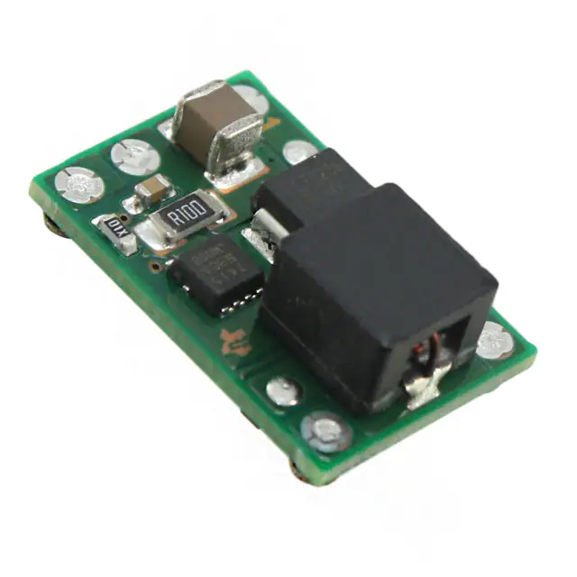
PTN78000A
www.ti.com
SLTS246B – APRIL 2005 – REVISED JANUARY 2006
1.5-A, WIDE-INPUT ADJUSTABLE BUCK-BOOST SWITCHING REGULATOR
FEATURES
•
•
•
•
•
•
•
•
APPLICATIONS
1.5-A Output Current
Wide-Input Voltage
(7 V to 29 V)
Wide-Output Voltage Adjust
(–15 V to –3 V)
High Efficiency (Up to 84%)
Output Current Limit
Overtemperature Shutdown
Operating Temperature: –40°C to 85°C
Surface-Mount Package Available
•
General-Purpose, Industrial Controls,
HVAC Systems, Test and Measurement,
Medical Instrumentation, AC/DC Adaptors,
Vehicles, Marine, and Avionics
DESCRIPTION
The PTN78000A is a series of high-efficiency, buck-boost integrated switching regulators (ISR), that represent
the third generation in the evolution of the PT78NR100 series of products. In new designs, it should be
considered in place of the PT78NR100 series of single in-line pin (SIP) products. The PTN78000A is smaller and
lighter than its predecessor, and has either similar or improved electrical performance characteristics. The
caseless, double-sided package also exhibits improved thermal characteristics, and is compatible with TI's
roadmap for RoHS and lead-free compliance.
Operating from a wide-input voltage range, the PTN78000A provides high-efficiency, positive-to-negative voltage
conversion for loads of up to 1.5 A. The output voltage is set using a single external resistor, and may be set to
any value within the range, –15 V to –3 V.
The PTN78000A has undervoltage lockout, and is suited to a wide variety of general-purpose applications that
operate off 12-V, 24-V, or tightly regulated 28-V dc power.
STANDARD APPLICATION
VI
1
2
PTN78000A
(Top View)
3
C1*
100 mF
Electrolytic
(Required)
GND
5
C2*
2 x 4.7 mF
Ceramic
(Required)
+
4
C3*
100 mF
Electrolytic
(Required)
RSET#
1 %, 0.05 W
(Required)
VO
GND
*See the Application Information for capacitor recommendation.
#RSET is required to adjust the output voltage lower than -3 V. See the Application Information for values.
Please be aware that an important notice concerning availability, standard warranty, and use in critical applications of Texas
Instruments semiconductor products and disclaimers thereto appears at the end of this data sheet.
PRODUCTION DATA information is current as of publication date.
Products conform to specifications per the terms of the Texas
Instruments standard warranty. Production processing does not
necessarily include testing of all parameters.
Copyright © 2005–2006, Texas Instruments Incorporated
�PTN78000A
www.ti.com
SLTS246B – APRIL 2005 – REVISED JANUARY 2006
These devices have limited built-in ESD protection. The leads should be shorted together or the device
placed in conductive foam during storage or handling to prevent electrostatic damage to the MOS gates.
ORDERING INFORMATION
PTN78000A (Basic Model)
Description
Pb – free and RoHS Compatible
Package
Designator
PTN78000AAH
Horizontal T/H
Yes
EUS
PTN78000AAS (1) (2)
Horizontal SMD
No
EUT
Horizontal SMD
Yes
EUT
Output Voltage
Part Number
–15 V to –3 V
(1) (3)
PTN78000AAZ
(1)
(2)
(3)
Add a T suffix for tape and reel option on SMD packages.
Standard option specifies Sn/Pb solder ball material.
Lead (Pb) - free option specifies Sn/Ag solder ball material.
ABSOLUTE MAXIMUM RATINGS
(1)
over operating free-air temperature range unless otherwise noted
all voltages with respect to GND (pin 1),
PTN78000A UNIT
TA
Over VI range
Wave solder temperature
Surface temperature of module body
or pins (5 seconds)
Solder reflow temperature
Surface temperature of module body
or pins
–40 to 85
Horizontal SMD (suffix
AH)
260
Horizontal SMD (suffix
AS)
235
Horizontal SMD (suffix
AZ)
260
Storage temperature
Tstg
(1)
Operating free-air temperature
°C
–40 to 125
Stresses beyond those listed under absolute maximum ratings may cause permanent damage to the device. These are stress ratings
only, and functional operation of the device at these or any other conditions beyond those indicated under recommended operating
conditions is not implied. Exposure to absolute-maximum-rated conditions for extended periods may affect device reliability.
RECOMMENDED OPERATING CONDITIONS
VI
Input voltage
TA
Operating free-air temperature
PO
Output power
MIN
MAX
UNIT
7
32 – |VO|
V
–40
85
°C
9
W
PACKAGE SPECIFICATIONS
PTN78000A (Suffix AH, AS, and AZ)
Weight
2 grams
Flammability
Meets UL 94 V-O
Mechanical shock
Per Mil-STD-883D, Method 2002.3, 1 ms, ½ sine,
mounted
Mechanical vibration
Mil-STD-883D, Method 2007.2, 20-2000 Hz
(1)
2
Qualification limit.
500 G
(1)
Horizontal T/H (suffix AH)
20 G
(1)
Horizontal SMD (suffix AS & AZ)
15 G
(1)
�PTN78000A
www.ti.com
SLTS246B – APRIL 2005 – REVISED JANUARY 2006
ELECTRICAL CHARACTERISTICS
operating at 25°C free-air temperature, VI = 12 V, VO = –5 V, IO = IO (max), C1 = 100 μF, C2 = 2x 4.7 μF, C3 = 100 μF (unless
otherwise noted)
PARAMETER
IO
Output current
VI
Input voltage range
VO
VO Adj
TEST CONDITIONS
TA = 85°C, natural convection airflow
Over IO range
IO (LIM)
TYP
0.6
VO = –12 V
0.1
0.75
(1)
VO = –5 V
0.1
1.5
(1)
VO = –3.3 V
0.1
1.5
(1)
VO = –15 V
7
17
(2)
VO = –12 V
7
20
(2)
VO = –5 V
7
27
(2)
VO = –3.3 V
7
28.7
(2)
±2%
(3)
TA = 25°C
Temperature variation
–40°C to 85°C
±0.5%
Line regulation
Over VI range
±10
Load regulation
Over IO range
±10
Total output voltage
variation
Includes set point, line, load
–40 < TA < 85°C
7 V ≤ VI ≤ (32 – |VO|) V
20-MHz bandwidth
Current limit threshold
ΔVO = –50 mV
–15
83%
VI = 12 V, RSET = 2 kΩ, VO = –12 V
84%
VI = 12 V, RSET = 28.7 kΩ, VO = –5 V
82%
VI = 12 V, RSET = 221 kΩ, VO = –3.3 V
77%
A
V
mV
(3)
–3
VI = 12 V, RSET = 100 Ω, VO = –15 V
UNIT
(1)
mV
±3%
Output voltage adjust
range
Output voltage ripple
MAX
0.1
Set-point voltage tolerance
Efficiency
η
MIN
VO = –15 V
V
V(PP)
2% VO
3.2
A
1 A/μs load step from 50% to 100% IOmax
Transient response
FS
Switching frequency
Over VI and IO ranges
UVLO
Undervoltage lockout
VI increasing
CI
External input capacitance
External output
capacitance
CO
MTBF
(1)
(2)
(3)
(4)
(5)
(6)
Calculated reliability
Recovery time
200
VO over/undershoot
1
440
660
5.5
Ceramic
9.4
(4)
Nonceramic
100
(4)
Ceramic
Nonceramic
100
(5)
Equivalent series resistance (nonceramic)
14
(6)
Per Telcordia SR-332, 50% stress,
TA = 40°C, ground benign
550
μs
%VO
8.9
kHz
V
μF
μF
200
μF
1,000
μF
mΩ
106 Hrs
The maximum output current is 1.5 A or the maximum output power is 9 W, whichever is less.
The maximum input voltage is limited and defined to be (32 – |VO|) volts.
The set-point voltage tolerance is affected by the tolerance and stability of RSET. The stated limit is unconditionally met if RSET has a
tolerance of 1% with 100 ppm/°C or better temperature stability.
A 100-μF electrolytic capacitor and two 4.7-μF ceramic capacitors are required across the input (VI and GND) for proper operation.
Locate the ceramic capacitance close to the module.
100 μF of output capacitance is required for proper operation. See the application information for further guidance.
This is the typical ESR for all the electrolytic (nonceramic) capacitance. Use 17 mΩ as the minimum when using maximum ESR values
to calculate.
3
�PTN78000A
www.ti.com
SLTS246B – APRIL 2005 – REVISED JANUARY 2006
PIN ASSIGNMENT
1
2
5
PTN78000A
(Top View)
4
3
TERMINAL FUNCTIONS
TERMINAL
NAME
NO.
I/O
1
O
VI
2
I
N/C
3
VO Adjust
4
I
GND
5
I/O
VO
4
DESCRIPTION
The negative output voltage power node with respect to the GND node. It is also the reference for the
VO Adjust control inputs.
The positive input voltage power node to the module, which is referenced to common GND.
This pin is active and must be isolated from any electrical connection.
A 1% resistor must be connected between pin 1 and pin 4 to set the output voltage of the module lower
than –3 V. If left open-circuit, the output voltage defaults to –3 V. The temperature stability of the resistor
should be 100 ppm/°C (or better). The set-point range is –15 V to –3 V. The standard resistor value for
a number of common output voltages is provided in the application information.
The common ground connection for the VI and VO power connections.
�PTN78000A
www.ti.com
SLTS246B – APRIL 2005 – REVISED JANUARY 2006
TYPICAL CHARACTERISTICS (7-V INPUT) (1) (2)
EFFICIENCY
vs
OUTPUT CURRENT
OUTPUT VOLTAGE RIPPLE
vs
OUTPUT CURRENT
75
VO = -12 V
70
65
VO = -15 V
60
VO = -5 V
VO = -3 V
55
50
45
0
0.3
0.6
0.9
1.2
VO = -12 V
120
VO = -15 V
100
80
60
40
VO = -5 V
20
VO = -3 V
0
0
1.5
1
VO = -5 V
0.5
VO = -3 V
0
1.2
0
1.5
0.3
0.6
0.9
1.2
1.5
Figure 2.
Figure 3.
TEMPERATURE DERATING
vs
OUTPUT CURRENT
TEMPERATURE DERATING
vs
OUTPUT CURRENT
TEMPERATURE DERATING
vs
OUTPUT CURRENT
90
90
Ambient Temperature - oC
Ambient Temperature - oC
1.5
Figure 1.
80
200 LFM
70
60
100 LFM
Nat conv
50
40
VO = -5 V
30
80
200 LFM
70
100 LFM
60
Nat conv
50
40
VO = -12 V
30
0
0.5
1
IO - Output Current - A
Figure 4.
(2)
0.9
VO = -15 V
IO - Output Current - A
90
(1)
0.6
VO = -12 V
2
IO - Output Current - A
IO - Output Current - A
20
0.3
1.5
Ambient Temperature - oC
Efficiency - %
80
2.5
140
PD - Power Dissipation - W
VO - Output Voltage Ripple - mVPP
90
85
POWER DISSIPATION
vs
OUTPUT CURRENT
80
200 LFM
70
100 LFM
60
Nat conv
50
40
VO = -15 V
30
20
20
0
0.25
0.5
IO - Output Current - A
Figure 5.
0.75
0
0.1
0.2
0.3
0.4
0.5
0.6
IO - Output Current - A
Figure 6.
The electrical characteristic data has been developed from actual products tested at 25°C. This data is considered typical for the
converter. Applies to Figure 1, Figure 2, and Figure 3.
The temperature derating curves represent the conditions at which internal components are at or below the manufacturer's maximum
operating temperatures. Derating limits apply to modules soldered directly to a 100 mm x 100 mm, double-sided PCB with 2 oz. copper.
For surface mount packages, multiple vias (plated through holes) are required to add thermal paths to the power pins. Please refer to
the mechanical specification for more information. Applies toFigure 4 ,Figure 5 , and Figure 6.
5
�PTN78000A
www.ti.com
SLTS246B – APRIL 2005 – REVISED JANUARY 2006
TYPICAL CHARACTERISTICS (12-V INPUT) (1) (2)
OUTPUT VOLTAGE RIPPLE
vs
OUTPUT CURRENT
75
70
VO = -12 V
65
VO = -15 V
60
VO = -5 V
55
VO = -3 V
50
45
0
0.5
1
1.5
100
2
VO = -15 V
90
80
70
VO = -12 V
60
50
40
VO = -5 V
30
20
VO = -3 V
10
0
0
IO - Output Current - A
VO = -5 V
0.6
0.4
VO = -3 V
0.2
0
0
0.5
1
1.5
IO - Output Current - A
TEMPERATURE DERATING
vs
OUTPUT CURRENT
TEMPERATURE DERATING
vs
OUTPUT CURRENT
TEMPERATURE DERATING
vs
OUTPUT CURRENT
Ambient Temperature - oC
Ambient Temperature - oC
1
0.8
Figure 9.
200 LFM
70
100 LFM
60
Nat conv
50
40
VO = -5 V and -3 V
0.5
90
80
200 LFM
70
100 LFM
60
Nat conv
50
40
VO = -12 V
30
20
1
IO - Output Current - A
Figure 10.
6
1.2
Figure 8.
80
0
1.4
1.5
90
30
(2)
1
VO = -12 V
Figure 7.
90
(1)
0.5
VO = -15 V
1.8
1.6
IO - Output Current - A
1.5
Ambient Temperature - oC
Efficiency - %
80
POWER DISSIPATION
vs
OUTPUT CURRENT
PD - Power Dissipation - W
90
85
VO - Output Voltage Ripple - mVPP
EFFICIENCY
vs
OUTPUT CURRENT
80
200 LFM
70
100 LFM
60
Nat conv
50
40
VO = -15 V
30
20
20
0
0.25
0.5
IO - Output Current - A
Figure 11.
0.75
0
0.1
0.2
0.3
0.4
0.5
0.6
IO - Output Current - A
Figure 12.
The electrical characteristic data has been developed from actual products tested at 25°C. This data is considered typical for the
converter. Applies to Figure 7, Figure 8, and Figure 9.
The temperature derating curves represent the conditions at which internal components are at or below the manufacturer's maximum
operating temperatures. Derating limits apply to modules soldered directly to a 100-mm x 100-mm, double-sided PCB with 2 oz. copper.
For surface mount packages, multiple vias (plated through holes) are required to add thermal paths to the power pins. Please refer to
the mechanical specification for more information. Applies to Figure 10, Figure 11, and Figure 12.
�PTN78000A
www.ti.com
SLTS246B – APRIL 2005 – REVISED JANUARY 2006
TYPICAL CHARACTERISTICS (24-V INPUT) (1) (2)
EFFICIENCY
vs
OUTPUT CURRENT
OUTPUT VOLTAGE RIPPLE
vs
OUTPUT CURRENT
80
VO = -5 V
Efficiency - %
75
70
65
VO = -3 V
60
55
50
45
0
0.3
0.6
0.9
1.2
70
2
1.8
60
VO = -5 V
50
PD - Power Dissipation - W
VO - Output Voltage Ripple - mVPP
85
POWER DISSIPATION
vs
OUTPUT CURRENT
40
30
20
VO = -3 V
10
0
VO = -5 V
1.2
1
0.8
VO = -3 V
0.6
0.4
0.2
0
0
1.5
1.6
1.4
0.3
0.9
0.6
1.2
1.5
Figure 13.
0
0.3
0.6
0.9
1.2
1.5
IO - Output Current - A
IO - Output Current - A
IO - Output Current - A
Figure 14.
Figure 15.
TEMPERATURE DERATING
vs
OUTPUT CURRENT
Ambient Temperature - oC
90
80
70
200 LFM
100 LFM
60
Nat conv
50
40
VO = -5V and -3 V
30
20
0
0.5
1
IO - Output Current - A
1.5
Figure 16.
(1)
(2)
The electrical characteristic data has been developed from actual products tested at 25°C. This data is considered typical for the
converter. Applies to Figure 13, Figure 14, and Figure 15.
The temperature derating curves represent the conditions at which internal components are at or below the manufacturer's maximum
operating temperatures. Derating limits apply to modules soldered directly to a 100-mm x 100-mm, double-sided PCB with 2 oz. copper.
For surface mount packages, multiple vias (plated through holes) are required to add thermal paths to the power pins. Please refer to
the mechanical specification for more information. Applies to Figure 16.
7
�PTN78000A
www.ti.com
SLTS246B – APRIL 2005 – REVISED JANUARY 2006
APPLICATION INFORMATION
Adjusting the Output Voltage of the PTN78000A Wide-Output Adjust Power Modules
General
A resistor must be connected directly between the VO Adjust control (pin 4) and the output voltage (pin 7) to set
the output voltage lower than –3 V. The adjustment range is from –15 V to –3 V. If pin 4 is left open, the output
voltage defaults to the highest value, –3 V.
Table 1 gives the standard resistor value for a number of common voltages, and with the actual output voltage
that the value produces. For other output voltages, the resistor value can either be calculated using the following
formula, or simply selected from the range of values given in Table 2. Figure 17 shows the placement of the
required resistor.
RSET = 54.9 kW ´
1.25 V
|VO| - 3 V
- 5.62 kW
Input Voltage Considerations
The PTN78000A is a buck-boost switching regulator. In order that the output remains in regulation, the input
voltage must not exceed the output by a maximum differential voltage.
For satisfactory performance, the maximum operating input voltage is (32 - |VO|) volts.
As an example, Table 1 gives the operating input voltage range for the common output bus voltages. In addition,
the Electrical Characteristics define the available output voltage adjust range for various input voltages.
Table 1. Standard Values of Rset for Common Output
Voltages
VO
(Required)
RSET
(Standard Value)
VO
(Actual)
Operating
VI Range
–15 V
100 Ω
–14.997 V
9 V to 17 V
–12 V
2 kΩ
–12.006 V
9 V to 20 V
–5 V
28.7 kΩ
–5.000 V
9 V to 27 V
–3.3 V
221 kΩ
–3.303 V
9 V to 28.7 V
PTN78000A
VI
2
VI
GND
Adj
VO
4
1
+
C1
C2
GND
5
RSET
0.05 W
1%
+
C3
VO
GND
(1)
A 0.05-W rated resistor may be used. The tolerance should be 1%, with a temperature stability of 100 ppm/°C (or
better). Place the resistor as close to the regulator as possible. Connect the resistor directly between pins 4 and 1
using dedicated PCB traces.
(2)
Never connect capacitors from VO Adjust to either GND or VO. Any capacitance added to the VO Adjust pin affects the
stability of the regulator.
Figure 17. VO Adjust Resistor Placement
8
�PTN78000A
www.ti.com
SLTS246B – APRIL 2005 – REVISED JANUARY 2006
Table 2. Output Voltage Set-Point Resistor Values
VO Required
RSET
VO Required
RSET
VO Required
RSET
–15.0 V
99 Ω
–11.9 V
2.09 kΩ
–8.8 V
6.21 kΩ
–14.9 V
147 Ω
–11.8 V
2.18 kΩ
–8.6 V
6.63 kΩ
–14.8 V
196 Ω
–11.7 V
2.27 kΩ
–8.4 V
7.09 kΩ
–14.7 V
245 Ω
–11.6 V
2.36 kΩ
–8.2 V
7.58 kΩ
–14.6 V
296 Ω
–11.5 V
2.45 kΩ
–8.0 V
8.11 kΩ
–14.5 V
347 Ω
–11.4 V
2.55 kΩ
–7.8 V
8.68 kΩ
–14.4 V
400 Ω
–11.3 V
2.65 kΩ
–7.6 V
9.30 kΩ
–14.3 V
453 Ω
–11.2 V
2.75 kΩ
–7.4 V
9.98 kΩ
–14.2 V
507 Ω
–11.1 V
2.82 kΩ
–7.2 V
10.7 kΩ
–14.1 V
562 Ω
–11.0 V
2.96 kΩ
–7.0 V
11.5 kΩ
–14.0 V
619 Ω
–10.9 V
3.07 kΩ
–6.8 V
12.4 kΩ
–13.9 V
676 Ω
–10.8 V
3.18 kΩ
–6.6 V
13.4 kΩ
–13.8 V
734 Ω
–10.7 V
3.29 kΩ
–6.4 V
14.6 kΩ
–13.7 V
794 Ω
–10.6 V
3.41 kΩ
–6.2 V
15.8 kΩ
–13.6 V
854 Ω
–10.5 V
3.53 kΩ
–6.0 V
17.3 kΩ
–13.5 V
916 Ω
–10.4 V
3.65 kΩ
–5.8 V
18.9 kΩ
–13.4 V
979 Ω
–10.3 V
3.78 kΩ
–5.6 V
20.7 kΩ
–13.3 V
1.04 kΩ
–10.2 V
3.91 kΩ
–5.4 V
22.9 kΩ
–13.2 V
1.11 kΩ
–10.1 V
4.04 kΩ
–5.2 V
25.6 kΩ
–13.1 V
1.18 kΩ
–10.0 V
4.18 kΩ
–5.0 V
28.7 kΩ
–13.0 V
1.24 kΩ
–9.9 V
4.33 kΩ
–4.8 V
32.5 kΩ
–12.9 V
1.31 kΩ
–9.8 V
4.47 kΩ
–4.6 V
37.2 kΩ
–12.8 V
1.38 kΩ
–9.7 V
4.62 kΩ
–4.4 V
43.4 kΩ
–12.7 V
1.46 kΩ
–9.6 V
4.78 kΩ
–4.2 V
51.6 kΩ
–12.6 V
1.52 kΩ
–9.5 V
4.94 kΩ
–4.0 V
63.0 kΩ
–12.5 V
1.60 kΩ
–9.4 V
5.10 kΩ
–3.8 V
80.1 kΩ
–12.4 V
1.68 kΩ
–9.3 V
5.27 kΩ
–3.6 V
109 kΩ
–12.3 V
1.76 kΩ
–9.2 V
5.45 kΩ
–3.4 V
166 kΩ
–12.2 V
1.84 kΩ
–9.1 V
5.63 kΩ
–3.2 V
338 kΩ
–12.1 V
1.92 kΩ
–9.0 V
5.82 kΩ
–3.0 V
OPEN
–12.0 V
2.01 kΩ
–8.9 V
6.01 kΩ
9
�PTN78000A
SLTS246B – APRIL 2005 – REVISED JANUARY 2006
www.ti.com
CAPACITOR RECOMMENDATIONS FOR THE PTN78000 WIDE-OUTPUT
ADJUST POWER MODULES
Input Capacitor
The minimum requirements for the input bus is 100 μF of nonceramic capacitance and 9.4 μF (2 x 4.7 μF) of
ceramic capacitance, in either an X5R or X7R temperature characteristic, and 100 μF of electrolytic capacitance.
Ceramic capacitors should be located within 0.5 inch (1,27 cm) of the regulator's input pins. Electrolytic
capacitors should be used at the input in addition to the required ceramic capacitance. The minimum ripple
current rating for any nonceramic capacitance must be at least 250 mA rms. The ripple current rating of
electrolytic capacitors is a major consideration when they are used at the input. This ripple current requirement
can be reduced by placing more ceramic capacitors at the input, in addition to the minimum required 9.4 μF.
Tantalum capacitors are not recommended for use at the input bus, as none were found to meet the minimum
voltage rating of 2 × (maximum dc voltage + ac ripple). The 2× rating is standard practice for regular tantalum
capacitors to ensure reliability. Polymer-tantalum capacitors are more reliable and are available with a maximum
rating of typically 20 V. These can be used with input voltages up to 16 V.
Output Capacitor
The minimum capacitance required to ensure stability is a 100 μF. Either ceramic or electrolytic-type capacitors
can be used. The minimum ripple current rating for the nonceramic capacitance must be at least 200 mA rms.
The stability of the module and voltage tolerances is compromised if the capacitor is not placed near the output
bus pins. A high-quality, computer-grade electrolytic capacitor should be adequate. A ceramic capacitor can be
also be located within 0.5 inch (1,27 cm) of the output pin.
For applications with load transients (sudden changes in load current), the regulator response improves with
additional capacitance. Additional electrolytic capacitors should be located close to the load circuit. These
capacitors provide decoupling over the frequency range, 2 kHz to 150 kHz. Aluminum electrolytic capacitors are
suitable for ambient temperatures above 0°C. For operation below 0°C, tantalum or Os-Con-type capacitors are
recommended. When using one or more nonceramic capacitors, the calculated equivalent ESR should be no
lower than 14 mΩ (17 mΩ using the manufacturer's maximum ESR for a single capacitor). A list of recommended
capacitors and vendors are identified in Table 3.
Ceramic Capacitors
Above 150 kHz, the performance of aluminum electrolytic capacitors becomes less effective. To further reduce
the reflected input ripple current, or the output transient response, multilayer ceramic capacitors must be added.
Ceramic capacitors have low ESR, and their resonant frequency is higher than the bandwidth of the regulator.
When placed at the output, their combined ESR is not critical as long as the total value of ceramic capacitance
does not exceed 200 μF.
Tantalum Capacitors
Tantalum-type capacitors may be used at the output, and are recommended for applications where the ambient
operating temperature can be less than 0°C. The AVX TPS, Sprague 593D/594/595, and Kemet
T495/T510/T520 capacitors series are suggested over many other tantalum types due to their rated surge, power
dissipation, and ripple current capability. As a caution, many general-purpose tantalum capacitors have
considerably higher ESR, reduced power dissipation, and lower ripple current capability. These capacitors are
also less reliable as they have lower power dissipation and surge current ratings. Tantalum capacitors that do not
have a stated ESR or surge current rating are not recommended for power applications. When specifying
Os-Con and polymer-tantalum capacitors for the output, the minimum ESR limit is encountered well before the
maximum capacitance value is reached.
Capacitor Table
The capacitor table, Table 3, identifies the characteristics of capacitors from various vendors with acceptable
ESR and ripple current (rms) ratings. The recommended number of capacitors required at both the input and
output buses is identified for each capacitor type. This is not an extensive capacitor list. Capacitors from other
vendors are available with comparable specifications. Those listed are for guidance. The rms rating and ESR (at
100 kHz) are critical parameters necessary to ensure both optimum regulator performance and long capacitor
life.
10
�PTN78000A
www.ti.com
SLTS246B – APRIL 2005 – REVISED JANUARY 2006
Designing for Load Transients
The transient response of the dc/dc converter has been characterized using a load transient with a di/dt of
1 A/μs. The typical voltage deviation for this load transient is given in the data sheet specification table using the
required value of output capacitance. As the di/dt of a transient is increased, the response of a converter's
regulation circuit ultimately depends on its output capacitor decoupling network. This is an inherent limitation of
any dc/dc converter once the speed of the transient exceeds its bandwidth capability. If the target application
specifies a higher di/dt or lower voltage deviation, the requirement can only be met with additional output
capacitor decoupling. In these cases, special attention must be paid to the type, value, and ESR of the
capacitors selected.
If the transient performance requirements exceed those specified in the data sheet, the selection of output
capacitors becomes more important. Review the minimum ESR in the characteristic data sheet for details on the
capacitance maximum.
Table 3. Recommended Input/Output Capacitors
CAPACITOR CHARACTERISTICS
QUANTITY
WORKING
VOLTAGE
(V)
VALUE
(μF)
EQUIVALENT
SERIES
RESISTANCE
(ESR) (Ω)
85°C
MAXIMUM
RIPPLE
CURRENT
(Irms) (mA)
FC( Radial)
35
100
0.117
550
8 × 11,5
FC (SMD)
35
100
0.015
670
10 × 10,2
United Chemi-Con PXA (SMD)
16
180
0.016
4360
PS
25
100
0.020
LXZ
50
100
MVY(SMD)
50
Nichicon UWG (SMD)
F550 (Tantalum)
CAPACITOR VENDOR/
COMPONENT
SERIES
PHYSICAL
SIZE
(mm)
INPUT OUTPUT
BUS
BUS
VENDOR
NUMBER
1
EEUFC1H181
≥1
(1)
1
EEVFC1V101P
8 × 12
≥1
(1)
≤1
4300
8 × 10,5
≥1
(1)
≤1
0.220
485
8 × 12,5
≥1
1
LXZ50VB101M8X12LL
100
0.300
500
10 × 10
≥1
1
MVY50VC101M10X10TP
(|VO| ≤ 5 V)
50
100
0.300
500
10 × 10
1
UWG1H101MNR1GS
10
100
0.055
2000
7.7 × 4,3
HD
50
120
0.072
979
10 × 12,5
Sanyo Os-Con SVP (SMD)
20
100
0.024
2500
8 × 12
≥1
(1)
≤1
SP
16
100
0.032
2890
10 × 5
≥1
(1)
≤1
16SP100M (VI, |VO| ≤ 14 V)
7,3 L × 4,3
W × 4,1 H
≥1
≥1
N/R
F551A107MN (|VO| ≤ 5 V)
UHD1H101MPR
20SVP100M (VI, |VO| ≤ 16 V)
N/R
(3)
≤2
N/R
(3)
≤2
TPSE107M020R0200
(|VO| ≤ 10 V)
≤2
GRM32ER61C476M
(|Vo| ~ VI≤ 13.5 V)
(1)
≤2
GRM422X5R476M6.3
(|VO| ≤ 5.5 V)
≥4
(4)
1
C3225X7R1E225KT/MT
(|VO| ≤ 20 V)
3225
≥4
(4)
1
GRM32RR71E225K
(|VO| ≤ 20 V)
>1000
3225
≥4
(4)
1
C1210C225K3RAC
(|VO| ≤ 20 V)
0.002
>1000
3225
≥4
(4)
1
12103C225KAT2A
(|VO| ≤ 20 V)
4.7
0.002
>1000
3225
≥2
1
GRM32ER71H475KA88L
2.2
0.002
>1000
≥4
1
C3225X7R1H225KT
2.2
0.004
>1000
≥4
1
RPER71H2R2KK6F03
100
0.085
1543
20
100
0.200
> 817
Murata X5R Ceramic
16
47
0.002
>1000
3225
1
Murata X5R Ceramic
6.3
47
0.002
>1000
3225
N/R
TDK X7R Ceramic
25
2.2
0.002
>1000
SMD
Murata X7R Ceramic
25
2.2
0.002
>1000
Kemet X7R Ceramic
25
2.2
0.002
AVX X7R Ceramic
25
2.2
Murata X7R Ceramic
50
TDK X7R Ceramic
50
Murata Radial Through-hole
50
(3)
(4)
1
≥1
20
(2)
≤ 3 (2)
10FS100M (VI, |VO| < 22 V)
TPSV107M020R0085
(|VO| ≤ 10 V)
AVX Tantalum TPS (SMD)
(1)
(1)
PXA16VC180MF60 (VI, |VO| <
14 V)
(1)
The voltage rating of the input capacitor must be selected for the desired operating input voltage range of the regulator. To operate the
regulator at a higher input voltage, select a capacitor with the next higher voltage rating.
The maximum voltage rating of the capacitor must be selected for the desired set-point voltage (VO ). To operate at a higher output
voltage, select a capacitor with a higher voltage rating.
Not recommended (N/R). The voltage rating does not meet the minimum operating limits in most applications.
The maximum rating of the ceramic capacitor limits the regulator's operating input voltage to 20 V. Select a alternative ceramic
component to operate at a higher input voltage.
11
�PTN78000A
www.ti.com
SLTS246B – APRIL 2005 – REVISED JANUARY 2006
Power-Up Characteristics
When configured per the standard application, the PTN78000A power module produces a regulated output
voltage following the application of a valid input source voltage. During power up, internal soft-start circuitry slows
the rate that the output voltage rises, thereby limiting the amount of in-rush current that can be drawn from the
input source. The soft-start circuitry introduces a short time delay (typically 5 ms – 10 ms) into the power-up
characteristic. This is from the point that a valid input source is recognized. Figure 18 shows the power-up
waveforms for a PTN78000A, operating from a 12-V input and with the output voltage adjusted to –5 V. The
waveforms were measured with a 1.5-A resistive load.
VI (5 V/div)
VO (2 V/div)
II (1 A/div)
t - Time = 5 ms/div
Figure 18. Power-Up Waveforms
Undervoltage Lockout
The undervoltage lockout (UVLO) circuit prevents the module from attempting to power up until the input voltage
is above the UVLO threshold. This prevents the module from drawing excessive current from the input source at
power up. Below the UVLO threshold, the module is held off.
Current Limit Protection
The PTN78000 modules protect against load faults with a continuous current limit characteristic. Under a load
fault condition, the output current cannot exceed the current limit value. Attempting to draw current that exceeds
the current limit value causes the module to progressively reduce its output voltage. Current is continuously
supplied to the fault until it is removed. On removal of the fault, the output voltage promptly recovers. When
limiting output current, the regulator experiences higher power dissipation, which increases its temperature. If the
temperature increase is excessive, the module's overtemperature protection begins to periodically turn the output
voltage completely off.
Overtemperature Protection
A thermal shutdown mechanism protects the module's internal circuitry against excessively high temperatures. A
rise in temperature may be the result of a drop in airflow, a high ambient temperature, or a sustained current-limit
condition. If the junction temperature of the internal control IC rises excessively, the module turns itself off,
reducing the output voltage to zero. The module instantly restarts when the sensed temperature decreases by a
few degrees.
Note: Overtemperature protection is a last-resort mechanism to prevent damage to the module. It should not be
relied on as permanent protection against thermal stress. Always operate the module within its temperature
derated limits, for the worst-case operating conditions of output current, ambient temperature, and airflow.
Operating the module above these limits, albeit below the thermal shutdown temperature, reduces the long-term
reliability of the module.
12
�PTN78000A
www.ti.com
SLTS246B – APRIL 2005 – REVISED JANUARY 2006
Optional Input/Output Filters
Power modules include internal input and output ceramic capacitors in all their designs. However, some
applications require much lower levels of either input reflected or output ripple/noise. This application describes
various filters and design techniques found to be successful in reducing both input and output ripple/noise.
Input/Output Capacitors
The easiest way to reduce output ripple and noise is to add one or more 1-μF ceramic capacitors, such as C5
shown in Figure 19. Ceramic capacitors should be placed close to the output power terminals. A single 4.7-μF
capacitor reduces the output ripple/noise by 10% to 30% for modules with a rated output current of less than 3 A.
(Note: C4 is recommended to improve the regulators transient response and does not reduce output ripple and
noise.)
Switching regulators draw current from the input line in pulses at their operating frequency. The amount of
reflected (input) ripple/noise generated is directly proportional to the equivalent source impedance of the power
source including the impedance of any input lines. The addition of C1, minimum 4.7-μF ceramic capacitor, near
the input power pins, reduces reflected conducted ripple/noise by 20% to 30%.
VI
2
PTN78000A
VO
VI
GND
5
C1
4.7 mF
Ceramic
C2
100 mF
Electrolytic
(Required)
C3
2 x 4.7 mF
Ceramic
(Required)
(See Note A)
VO
1
Adj
4
RSET
C4
100 mF
(Required)
(See Note B)
GND
C5
4.7 mF
Ceramic
GND
A.
See specifications for required value and type.
B.
See Application Information for suggested value and type.
Figure 19. Adding High-Frequency Bypass Capacitors to the Input and Output
π Filters
If a further reduction in ripple/noise level is required for an application, higher order filters must be used. A π (pi)
filter, employing a ferrite bead (Fair-Rite Pt. No. 2673000701 or equivalent) in series with the input or output
terminals of the regulator reduces the ripple/noise by at least 20 db (see Figure 20 and Figure 21). In order for
the inductor to be effective in reduction of ripple and noise ceramic capacitors are required. (See the Capacitor
Recommendations for the PTN78000A for additional information on vendors and component suggestions.)
These inductors plus ceramic capacitors form an excellent filter because of the rejection at the switching
frequency (650 kHz - 1 MHz). The placement of this filter is critical. It must be located as close as possible to the
input or output pins to be effective. The ferrite bead is small (12,5 mm × 3 mm), easy to use, low cost, and has
low dc resistance. Fair-Rite also manufactures a surface-mount bead (part number 2773021447), through hole
(part number 2673000701) rated to 5 A. Alternatively, 1-μH to 5-μH inductors can be used in place of the ferrite
inductor bead.
13
�PTN78000A
www.ti.com
SLTS246B – APRIL 2005 – REVISED JANUARY 2006
L1
1 - 5 mH
VI
2
VI
PTN78000A
GND
C2
100 mF
Electrolytic
(Required)
1
4
C3
2 x 4.7 mF
Ceramic
(Required)
(See Note A)
C4
100 mF
(Required)
(See Note B)
RSET
GND
C5
4.7 mF
Ceramic
C6
(See Note C)
GND
A.
See specifications for required value and type.
B.
See Application Information for suggested value and type.
C.
Recommended for applications with load transients.
Figure 20. Adding π Filters (IO≤ 3 A)
45
40
Attenuation − dB
35
1 MHz
30
25
600 kHz
20
15
10
0
0.5
1
1.5
2
Load Current − A
2.5
3
Figure 21. π-Filter Attenuation vs. Load Current
14
VO
Adj
5
C1
4.7 mF
Ceramic
VO
L2
1 - 5 mH
�PACKAGE OPTION ADDENDUM
www.ti.com
8-Mar-2022
PACKAGING INFORMATION
Orderable Device
Status
(1)
Package Type Package Pins Package
Drawing
Qty
Eco Plan
(2)
Lead finish/
Ball material
MSL Peak Temp
Op Temp (°C)
(3)
Device Marking
(4/5)
(6)
PTN78000AAH
ACTIVE
ThroughHole Module
EUS
5
56
RoHS (In
Work) & Green
(In Work)
SN
N / A for Pkg Type
-40 to 85
PTN78000AAS
ACTIVE
Surface
Mount Module
EUT
5
49
Non-RoHS
& Green
(In Work)
SNPB
Level-1-235C-UNLIM/
Level-3-260C-168HRS
-40 to 85
PTN78000AAST
ACTIVE
Surface
Mount Module
EUT
5
250
Non-RoHS
& Green
(In Work)
SNPB
Level-1-235C-UNLIM/
Level-3-260C-168HRS
-40 to 85
PTN78000AAZ
ACTIVE
Surface
Mount Module
EUT
5
49
RoHS (In
Work) & Green
SNAGCU
Level-3-260C-168 HR
-40 to 85
PTN78000AAZT
ACTIVE
Surface
Mount Module
EUT
5
250
RoHS (In
Work) & Green
SNAGCU
Level-3-260C-168 HR
-40 to 85
(1)
The marketing status values are defined as follows:
ACTIVE: Product device recommended for new designs.
LIFEBUY: TI has announced that the device will be discontinued, and a lifetime-buy period is in effect.
NRND: Not recommended for new designs. Device is in production to support existing customers, but TI does not recommend using this part in a new design.
PREVIEW: Device has been announced but is not in production. Samples may or may not be available.
OBSOLETE: TI has discontinued the production of the device.
(2)
RoHS: TI defines "RoHS" to mean semiconductor products that are compliant with the current EU RoHS requirements for all 10 RoHS substances, including the requirement that RoHS substance
do not exceed 0.1% by weight in homogeneous materials. Where designed to be soldered at high temperatures, "RoHS" products are suitable for use in specified lead-free processes. TI may
reference these types of products as "Pb-Free".
RoHS Exempt: TI defines "RoHS Exempt" to mean products that contain lead but are compliant with EU RoHS pursuant to a specific EU RoHS exemption.
Green: TI defines "Green" to mean the content of Chlorine (Cl) and Bromine (Br) based flame retardants meet JS709B low halogen requirements of


 工商网监
湘ICP备2023018690号
工商网监
湘ICP备2023018690号
