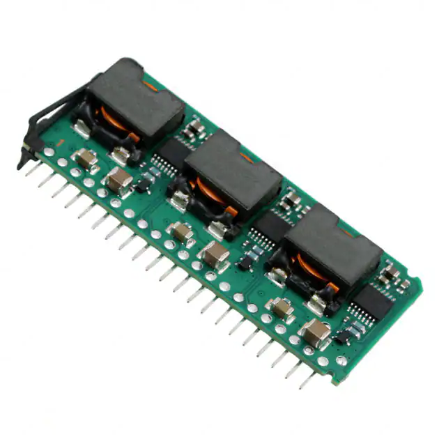
PTV08040W
www.ti.com
SLTS257B – SEPTEMBER 2005 – REVISED JANUARY 2008
50-A, 8-V to 14-V INPUT, NON-ISOLATED, WIDE-OUTPUT
ADJUST, VERTICAL POWER MODULE
FEATURES
APPLICATIONS
•
•
•
•
•
•
•
•
1
2
•
•
•
•
•
•
•
50-A Output Current
8-V to 14-V Input Voltage
Wide-Output Voltage Adjust (0.8 V to 3.6 V)
Efficiencies up to 95%
On/Off Inhibit
Differential Output Sense
Output Overcurrent Protection
(Nonlatching, Auto-Reset)
Overtemperature Protection
Auto-Track™ Sequencing
Start Up Into Output Prebias
Operating Temperature: –40°C to 85°C
Multi-Phase, Switch-Mode Topology
Programmable Undervoltage Lockout (UVLO)
Safety Agency Approvals: (Pending)
UL/IEC/CSA-22.2 60950-1
Advanced Computing and Server Applications
DESCRIPTION
The PTV08040W is a high-performance 50-A rated, non-isolated, power module, that uses the latest multi-phase
switched-mode topology. This provides a small, ready-to-use module, that can power the most densely populated
multiprocessor systems. The PTV08040W is produced in a 21-pin, single in-line pin (SIP) package. The SIP
footprint minimizes board space, and offers an alternate package option for space conscious applications. The
modules use double-sided surface mount construction to provide a low profile and compact footprint.
Operating from an input voltage range of 8 V to 14 V, the PTV08040W requires a single resistor to set the output
voltage to any value over the range, 0.8 V to 3.6 V. The wide input voltage range makes the PTV08040W
particularly suitable for advanced computing and server applications that utilize a loosely regulated intermediate
distribution bus of 8 V to 14 V.
The PTV08040W incorporates Auto-Track™ sequencing. The Auto-Track feature of the PTH and PTV family
allows the outputs of multiple modules to track a common voltage during power up and power down transitions.
This simplifies power up and power down supply-voltage sequencing in a power supply system.
The module incorporates a comprehensive list of features. They include on/off inhibit, a differential remote output
voltage sense which ensures tight load regulation, and an output overcurrent and overtemperature shutdown to
protect against load faults. The programmable undervoltage lockout allows the turn-on and turn-off voltage
thresholds to be customized.
1
2
Please be aware that an important notice concerning availability, standard warranty, and use in critical applications of
Texas Instruments semiconductor products and disclaimers thereto appears at the end of this data sheet.
Auto-Track, TMS320 are trademarks of Texas Instruments.
PRODUCTION DATA information is current as of publication date.
Products conform to specifications per the terms of the Texas
Instruments standard warranty. Production processing does not
necessarily include testing of all parameters.
Copyright © 2005–2008, Texas Instruments Incorporated
�PTV08040W
www.ti.com
SLTS257B – SEPTEMBER 2005 – REVISED JANUARY 2008
These devices have limited built-in ESD protection. The leads should be shorted together or the device placed in conductive foam
during storage or handling to prevent electrostatic damage to the MOS gates.
STANDARD APPLICATION
Track
9
15
N/C
Track
6,7
VI
13,14
20,21
VI
PTV08040W
16 Inhibit/
UVLO Prog
GND
12 18 19
VO
-Sense
GND
4 5 11
+ Sense
+Sense 1
3
VO
10
17
2
VOAdj
8
CI
L
O
A
D
CO
560 mF
(Required)
150 mF
Ceramic
(Required)
RSET
1%
0.05 W
– Sense
GND
A.
GND
RSET = Required to set the output voltage higher than the minimum value (see the electrical characteristic for values.)
ORDERING INFORMATION
For the most current package and ordering information, see the Package Option Addendum at the end of this datasheet, or see
the TI website at www.ti.com.
ABSOLUTE MAXIMUM RATINGS
over operating free-air temperature range (unless otherwise noted)
UNIT
Track pin voltage
Track control (pin 15)
TA
Operating temperature
range
Over VI range
Twave
Wave solder
temperature
Surface temperature of module pins (5 seconds)
Tstg
Storage temperature
–40°C to 85°C
260°C
–55°C to 125°C
Mechanical shock
Per Mil-STD-883D, Method 2002.3, 1 msec, Sine, mounted
500 G
Mechanical vibration
Mil-STD-883D, Method 2007.2, 20–2000 Hz
15 G
Weight
Flammability
2
–0.3 V to VI + 0.3 V
16.6 grams
Meets UL94V-O
Submit Documentation Feedback
Copyright © 2005–2008, Texas Instruments Incorporated
Product Folder Link(s): PTV08040W
�PTV08040W
www.ti.com
SLTS257B – SEPTEMBER 2005 – REVISED JANUARY 2008
ELECTRICAL CHARACTERISTICS
TA = 25°C, VI = 12 V, VO = 3.3 V, CI = 560 µF, CO = 150 F, and IO = IOmax (unless otherwise stated)
PARAMETER
TEST CONDITIONS
MIN
TYP
MAX
25°C, Natural Convection
0
50 (1)
60°C, 200 LFM airflow
0
48 (1)
UNIT
IO
Output current
8 V ≤ VI ≤ 14 V
VI
Input voltage range
Over IO range
VOtol
Set-point voltage tolerance
ΔRegtemp
Temperature variation
–40°C < TA < 85°C
±0.5
%VO
ΔRegline
Line regulation
Over VI range
±3
mV
ΔRegload
Load regulation
Over IO range
±3
ΔRegtot
Total output variation
Includes set-point, line, load, –40°C ≤ TA ≤ 85°C
ΔRegadj
Output adjust range
η
Efficiency
IOtrip
trr
14
±2 (2)
95
RSET = 6.98 kΩ, VO = 2.5 V
93
RSET = 13.0 kΩ, VO = 2 V
92
RSET = 16.9 kΩ, VO = 1.8 V
91
RSET = 27.4 kΩ, VO = 1.5 V
90
RSET = 53.6 kΩ, VO = 1.2 V
88
RSET = 113.0 kΩ, VO = 1 V
86
RSET = open circuit, VO = 0.8 V
82
All voltages
15
IO = 35 A
20-MHz bandwidth
Overcurrent threshold
Reset, followed by auto-recovery
75
1 A/µs load step,
50 to 100% IOmax, CO = 150 µF
IILtrack
Track input current (pin 15)
Pin to GND
dVtrack/dt
Track slew rate capability
CO ≤ CO(max)
UVLO
Undervoltage lockout threshold
Pin 16 open
Inhibit control (pin 16)
Referenced to GND
3.6
RSET = 2.49 kΩ, VO = 3.3 V
100
Recovery time
50
VO over/undershoot
140
7.5 (4)
VI Decreasing
6
115
mV
(3)
mA
1
V/ms
7.8
Input high voltage
2.5
Open (5)
VIL
Input low voltage
–0.2
0.5
IILinhibit
Input low current
Pin to GND
0.5
IIinh
Input standby current
Pin 16 to GND
35
fs
Switching frequency
Over VI and IO ranges
CI
External input capacitance
CO
External output capacitance
MTBF
Reliability
(1)
(2)
(3)
(4)
(5)
(6)
(7)
(8)
(9)
V
V
mA
mA
1200
560 (6)
Capacitance value
A
µs
6.5 (4)
1050
V
mVPP
VIH
900
%VO
%
–0.13
VI Increasing
V
%VO
mV
±3 (2)
0.8
VO ripple (peak-to-peak)
Transient response
ΔVtr
8
A
kHz
µF
Nonceramic
0
14,000 (7)
Ceramic
150 (8)
750
µF
Equivalent series resistance (nonceramic)
3 (9)
mΩ
Per Bellcore TR-332 50% stress, TA = 40°C, ground benigh
2.7
106 Hrs
See SOA curves or consult factory for appropriate derating.
The set-point voltage tolerance is affected by the tolerance of RSET. The stated limit is unconditionally met if RSET has a tolerance of 1%
with 100 ppm/°C or better temperature stability.
This control pin has an internal pull-up to 5 V. A small, low-leakage (850 mA
10 × 10,2
1
1
EEVFK1C681P
1000
0.060 Ω
1100 mA
12,5 × 13,5
1
1
EEVFK1V102Q
25 V
470
0.090 Ω
670 mA
10 × 10
2
1
MVZ25VC471MJ10TP
16 V
470
0.090 Ω
760 mA
10 × 12,5
2
1
LXZ16VB471M10X12LL
16 V
680
0.068 Ω
1050 mA
10 × 16
1
1
LXZ16VB681M10X16LL
PS, Poly-Aluminum(Radial)
16 V
330
0.014 Ω
5060 mA
10 × 12,5
2
≤3
16PS330MJ12
PXA, Poly-Aluminum (SMD)
16 V
330
0.014 Ω
5050 mA
10 × 12,2
2
≤3
PXA16VC331MJ12TP
Nichicon, Aluminum
HD (Radial)
25 V
680
0.038 Ω
1430 mA
10 × 16
1
1
UHD1C681MHR
PM (Radial)
25 V
560
0.060 Ω
1060 mA
12,5 × 15
1
1
UPM1E561MHH6
35 V
560
0.048 Ω
1360 mA
16 × 15
1
1
UPM1V561MHH6
Panasonic, Poly-Aluminum
6.3 V
180
0.005 Ω
4000 mA
7,3 x 4,3 × 4,2
N/R (2)
≤4
EEFWA1C331P
Sanyo
TPE, Poscap (SMD)
10 V
330
0.025 Ω
3000 mA
7,3 × 5,7
N/R (2)
≤5
10TPE330M
SVP, OS-CON (SMD)
16 V
330
0.016 Ω
>4700 mA
10 × 12,6
2
≤3
16SVP330M
SEPC, OS-CON (Radial)
16 V
470
0.010Ω
>6000 mA
11 × 13
2
≤2
16SEPC470M
AVX, Tantalum, Series III
TPS (SMD)
10 V
470
0.045 Ω
>1723 mA
7,3 × 5,7 × 4,1
N/R (2)
≤7
TPSE477M010R0045
10 V
330
0.045 Ω
1723 mA
7,3 × 5,7 × 4,1
N/R (2)
≤7
TPSE337M010R0045
Kemet, Poly-Tantalum
T520 (SMD)
10 V
330
0.040 Ω
1800 mA
4,3 × 7,3 × 4
N/R (2)
≤7
T520X337M010AS
T530 (SMD)
10 V
330
0.015 Ω
>3800 mA
4,3 × 7,3 × 4
N/R (2)
≤3
T530X337M010AS
6.3 V
470
0.012 Ω
4200 mA
4,3 × 7,3 × 4
N/R (2)
≤2
T530X477M006AS
7,2 × 5,7 × 4,1
N/R (2)
Panasonic
FC (Radial)
FK (SMD)
Vendor Part No.
Vishay-Sprague
595D, Tantalum (SMD)
10 V
2
595D477X0010R2T
94SA, Os-con (Radial)
16 V
1000
0.015 Ω
9740 mA
16 × 25
1
≤3
94SA108X0016HBP
Kemet, Ceramic X5R (SMD)
16 V
6.3 V
10
47
0.002 Ω
0.002 Ω
–
3225
1
N/R (2)
≤10
≤10
C1210C106M4PAC
C1210C476K9PAC
Murata, Ceramic X5R (SMD)
6.3 V
6.3 V
16 V
16 V
16 V
100
47
47
22
10
–
–
3225
N/R (2)
N/R (2)
1
1
1
≤5
≤ 10
≤ 10
≤ 10
≤ 10
GRM32ER60J107M
GRM32ER60J476M
GRM32ER61C476K
GRM32ER61C226K
GRM32DR61C106K
TDK, Ceramic X5R (SMD)
6.3 V
6.3 V
16 V
16 V
100
47
22
10
–
–
3225
N/R (2)
N/R (2)
1
1
≤5
≤ 10
≤ 10
≤ 10
C3225X5R0J107MT
C3225X5R0J476MT
C3225X5R1C226MT
C3225X5R1C106MT
(1)
(2)
470
0.100 Ω
1440 mA
Capacitor Supplier Verification
1.Please verify availability of capacitors identified in this table. Capacitor suppliers may recommend alternative part numbers because of
limited availability or obsolete products. In some instances, the capacitor product life cycle may be in decline and have short-term
consideration for obsolescence.
RoHS, Lead-free and Material Details
2.Please consult capacitor suppliers regarding material composition, RoHS status, lead-free status, and manufacturing process
requirements. Component designators or part number deviations can occur when material composition or soldering requirements are
updated.
N/R – Not recommended. The voltage rating does not meet the minimum operating limits.
Submit Documentation Feedback
Copyright © 2005–2008, Texas Instruments Incorporated
Product Folder Link(s): PTV08040W
9
�PTV08040W
www.ti.com
SLTS257B – SEPTEMBER 2005 – REVISED JANUARY 2008
ADJUSTING THE OUTPUT VOLTAGE OF THE PTV08040W WIDE-OUTPUT ADJUST POWER
MODULE
The VO Adjust control (pin 8) sets the output voltage of the PTV08040W product. The adjustment range is from
0.8 V to 3.6 V. The adjustment method requires the addition of a single external resistor, RSET, that must be
connected directly between the VO Adjust and GND pins. Table 2 gives the preferred value of the external
resistor for a number of standard voltages, along with the actual output voltage that this resistance value
provides.
For other output voltages, the value of the required resistor can either be calculated using Equation 1, or simply
selected from the range of values given in Table 3. Figure 9 shows the placement of the required resistor.
RSET = 30.1 x
0.8
( VO - 0.8)
- 7.135 kW
(1)
Table 2. Standard Values of RSET for Common Output
Voltages
PTV08040W
VO (Required)
RSET
VO (Actual)
3.3 V
2.49 kΩ
3.303 V
2.5 V
6.98 kΩ
2.5 V
2.0 V
13.0 kΩ
1.997 V
1.8 V
16.9 kΩ
1.796 V
1.5 V
27.4 kΩ
1.498 V
1.2 V
53.6 kΩ
1.202 V
1.0 V
113 kΩ
1V
0.8 V
Open
0.8 V
+Sense
+Sense
1
3
PTV08040W
VO
-Sense
GND
GND
12 18 19 4 5 11
VO
10
17
2
VOAdj
8
CO1
RSET
1%
0.05 W
CO2
-Sense
GND
Figure 9. VO Adjust Resistor Placement
•
•
10
A 0.05-W rated resistor may be used. The tolerance should be 1%, and the temperature stability, 100 ppm/°C
(or better). Place the resistor as close to the regulator as possible. Connect the resistor directly between pin 8
and nearest GND pin (pin 11) using dedicated PCB traces.
Never connect capacitors from VO Adjust to either GND or VO. Any capacitance added to the VO Adjust pin
affects the stability of the regulator.
Submit Documentation Feedback
Copyright © 2005–2008, Texas Instruments Incorporated
Product Folder Link(s): PTV08040W
�PTV08040W
www.ti.com
SLTS257B – SEPTEMBER 2005 – REVISED JANUARY 2008
Table 3. Output Voltage Set-Point Resistor Values
VO
RSET
VO
RSET
VO
RSET
0.8
Open
1.375
34.8 kΩ
2.4
7.87 kΩ
0.825
953 kΩ
1.4
33.2 kΩ
2.45
7.50 kΩ
0.85
475 kΩ
1.425
31.6 kΩ
2.5
6.98 kΩ
0.875
316 kΩ
1.45
30.1 kΩ
2.55
6.65 kΩ
0.9
232 kΩ
1.475
28.7 kΩ
2.6
6.19 kΩ
0.925
187 kΩ
1.5
27.4 kΩ
2.65
5.90 kΩ
0.95
154 kΩ
1.55
24.9 kΩ
2.7
5.49 kΩ
0.975
130 kΩ
1.6
22.6 kΩ
2.75
5.23 kΩ
1
113 kΩ
1.65
21.0 kΩ
2.8
4.87 kΩ
1.025
100 kΩ
1.7
19.6 kΩ
2.85
4.64 kΩ
1.05
88.7 kΩ
1.75
18.2 kΩ
2.9
4.32 kΩ
1.075
80.6 kΩ
1.8
16.9 kΩ
2.95
4.02 kΩ
1.1
73.2 kΩ
1.85
15.8 kΩ
3
3.83 kΩ
1.125
66.5 kΩ
1.9
14.7 kΩ
3.05
3.57 kΩ
1.15
61.9 kΩ
1.95
13.7 kΩ
3.1
3.32 kΩ
1.175
57.6 kΩ
2
13.0 kΩ
3.15
3.09 kΩ
1.2
53.6 kΩ
2.05
12.1 kΩ
3.2
2.87 kΩ
1.225
49.9 kΩ
2.1
11.3 kΩ
3.25
2.67 kΩ
1.25
46.4 kΩ
2.15
10.7 kΩ
3.3
2.49 kΩ
1.275
43.2 kΩ
2.2
10.0 kΩ
3.35
2.32 kΩ
1.3
41.2 kΩ
2.25
9.53 kΩ
3.4
2.10 kΩ
1.325
38.3 kΩ
2.3
8.87 kΩ
3.5
1.78 kΩ
1.35
36.5 kΩ
2.35
8.45 kΩ
3.6
1.47 kΩ
Submit Documentation Feedback
Copyright © 2005–2008, Texas Instruments Incorporated
Product Folder Link(s): PTV08040W
11
�PTV08040W
www.ti.com
SLTS257B – SEPTEMBER 2005 – REVISED JANUARY 2008
ADJUSTING THE UNDERVOLTAGE LOCKOUT (UVLO) OF THE PTV08040W POWER MODULES
The PTV08040W power modules incorporate an input undervoltage lockout (UVLO). The UVLO feature prevents
the operation of the module until there is sufficient input voltage to produce a valid output voltage. This enables
the module to provide a clean, monotonic powerup for the load circuit, and also limits the magnitude of current
drawn from the regulator’s input source during the power-up sequence.
The UVLO characteristic is defined by the ON threshold (VTHD) and hysterisis (VHYS) voltages. Below the ON
threshold, the Inhibit control is overridden, and the module does not produce an output. The hysterisis voltage is
the difference between the ON and OFF threshold voltages. It ensures a clean power-up, even when the input
voltage is rising slowly. The hysterisis prevents start-up oscillations, which can occur if the input voltage droops
slightly when the module begins drawing current from the input source.
UVLO Adjustment
The UVLO feature of the PTV08040W module allows for limited adjustment of both the on threshold and
hysterisis voltages. The adjustment is made via the UVLO Prog control pin. When the UVLO Prog pin is left open
circuit, the ON threshold and hysterisis voltages are internally set to their default values. The ON threshold has a
nominal voltage of 7.5 V, and the hysterisis 1 V. This ensures that the module produces a regulated output when
the minimum input voltage is applied (see specifications). The combination correlates to an OFF threshold of
approximately 6.5 V. The adjustments are limited. The ON threshold can only be adjusted higher, and the
hysterisis voltage can only be reduced in magnitude.
The ON threshold might need to be raised if the module is powered from a tightly regulated 12-V bus. This
prevents it from operating if the input bus fails to completely rise to its specified regulation voltage. The hysterisis
should not be changed unless absolutely necessary. The hysterisis ensures that the module exhibits a clean
startup. Therefore, adjustment of the hysterisis should only be considered if there is a system requirement to
specifically set the off threshold voltage (in addition to the on threshold). Depending on the load regulation of the
input source, the hysterisis should not be adjusted below 0.5 V without careful consideration.
Adjustment Method
The resistors, RTHD and RHYS (see Figure 10), provide the adjustment of the on-threshold and hysterisis voltages.
RTHD connects between the UVLO Prog control pin and GND, and RHYS is connected between the UVLO Prog
and VI. RTHD alone is used to adjust the on-threshold voltage higher. However, to adjust the hystersis to a lower
value requires both the RHYS and RTHD resistors to be placed in the circuit.
The recommended adjustment method requires that any change to the hysterisis be determined first. If the
hysterisis is changed, then a value for RTHD must also be calculated. This is irrespective of whether a change is
required to the value of VTHD. If there is no change to VHYS, then a resistor should not be placed in the RHYS
location. RHYS should then be assigned an infinite value for calculating the value of RTHD.
6, 7
VI
13, 14
20, 21
RHYS
VI
PTV08040W
16 Inhibit/
UVLO Prog
GND
4
CI
5
11
RTHD
GND
Figure 10. UVLO Program Resistor Placement
12
Submit Documentation Feedback
Copyright © 2005–2008, Texas Instruments Incorporated
Product Folder Link(s): PTV08040W
�PTV08040W
www.ti.com
SLTS257B – SEPTEMBER 2005 – REVISED JANUARY 2008
Hysterisis Adjust
The hysterisis voltage, VHYS, is the difference between the ON and OFF threshold values. The default value is 1
V and it can only be adjusted to a lower value.
Caution should be used when changing the hysterisis voltage to a lower value, as it could permit start-up
oscillations.
Any change in the hysterisis voltage requires both RHYS and RTHD resistors be in place. Adding RHYS alone does
not have the desired effect. The value for RHYS must first be calculated using Equation 2, and then be used to
determine a value for RTHD, using Equation 3.
R HYS =
2 6 .1 ´ V H Y S
kΩ
0 .3 6 5 ´ (1 - V H Y S )
(2)
Threshold Adjust
Equation 3 determines the value of RTHD required to adjust VTHD to a new value. The default value is 7.5 V, and it
may only be adjusted to a higher value. If the hysterisis value has been adjusted, then a value for RTHD must also
be calculated. (This is irrespective of whether VTHD is being adjusted.) If there has been no adjustment for the
hystersis voltage, the term 1/RHYS in Equation 3, may be assigned the value, 0.
R THD =
39.2
kΩ
39.2[(1/R HYS + 0.014)(VTHD /2.5 - 1) - 0.0027] - 1
(3)
Calculated Values
Table 4 shows a matrix of standard resistor values for RHYS and RTHD, for different options of the on-threshold
(VTHD) and hysterisis (VHYS) voltages. For most applications, only the on-threshold voltage should need to be
adjusted. In this case select only a value for RTHD from far right-hand column.
The hysterisis should only be adjusted if there is a specific requirement to independently adjust the off-threshold,
separately from the on-threshold voltage. In this case, a value for both RHYS and RTHD must be selected from
Table 4. This is irrespective of whether the on-threshold voltage is being adjusted.
Table 4. Calculated Values of RHYS and RTHD, for Various Values of VHYS and
VTHD
VTHD
VHYS
0.5 V
RHYS
0.6 V
0.7 V
0.8 V
0.9 V
1V
(default)
71.5 kΩ
107 kΩ
165 kΩ
287 kΩ
649 kΩ
N/A
8V
30.1 kΩ
43.2 kΩ
63.4 kΩ
97.6 kΩ
169 kΩ
402 kΩ
8.5 V
25.5 kΩ
36.5 kΩ
51.1 kΩ
73.2 kΩ
110 kΩ
187 kΩ
9V
23.2 kΩ
30.9 kΩ
42.2 kΩ
57.6 kΩ
82.5 kΩ
124 kΩ
9.5 V
20 kΩ
27.4 kΩ
36.5 kΩ
48.7 kΩ
64.9 kΩ
90.9 kΩ
18.2 kΩ
24.3 kΩ
31.6 kΩ
41.2 kΩ
54.9 kΩ
73.2 kΩ
10.5 V
10 V
RTHD
16.2 kΩ
21.5 kΩ
28 kΩ
36.5 kΩ
46.4 kΩ
60.4 kΩ
11 V
15 kΩ
19.6 kΩ
25.5 kΩ
32.4 kΩ
41.2 kΩ
52.3 kΩ
11.5 V
14 kΩ
18.2 kΩ
23.2 kΩ
28 kΩ
36.5 kΩ
45.3 kΩ
12 V
12.7 kΩ
16.5 kΩ
21 kΩ
26.1 kΩ
32.4 kΩ
40.2 kΩ
Submit Documentation Feedback
Copyright © 2005–2008, Texas Instruments Incorporated
Product Folder Link(s): PTV08040W
13
�PTV08040W
www.ti.com
SLTS257B – SEPTEMBER 2005 – REVISED JANUARY 2008
FEATURES OF THE PTH/PTV FAMILY OF NONISOLATED WIDE OUTPUT ADJUST POWER
MODULES
Soft-Start Power Up
The Auto-Track feature allows the power-up of multiple PTH/PTV modules to be directly controlled from the
Track pin. However in a stand-alone configuration, or when the Auto-Track feature is not being used, the Track
pin should be directly connected to the input voltage, VI (see Figure 11).
15
Track
6, 7
VI
13, 14
20, 21
VI
PTV08040W
GND
CI
4
5
11
GND
Figure 11. Track Pin Connection
When the Track pin is connected to the input voltage the Auto-Track function is permanently disengaged. This
allows the module to power up entirely under the control of its internal soft-start circuitry. When power up is
under soft-start control, the output voltage rises to the set-point at a quicker and more linear rate.
From the moment a valid input voltage is applied, the soft-start control introduces a short time delay (typically
8 ms–15 ms) before allowing the output voltage to rise.
VI (5 V/div)
VO (1 V/div)
II (2 A/div)
t - Time = 4 ms/div
Figure 12. Power-Up Waveform
14
Submit Documentation Feedback
Copyright © 2005–2008, Texas Instruments Incorporated
Product Folder Link(s): PTV08040W
�PTV08040W
www.ti.com
SLTS257B – SEPTEMBER 2005 – REVISED JANUARY 2008
The output then progressively rises to the module’s setpoint voltage. Figure 12 shows the soft-start power-up
characteristic of the PTV08040W operating from a 12-V input bus and configured for a 3.3-V output. The
waveforms were measured with a 20-A constant current load and the Auto-Track feature disabled. The initial rise
in input current when the input voltage first starts to rise is the charge current drawn by the input capacitors.
Power-up is complete within 25 ms.
Overcurrent Protection
For protection against load faults, all modules incorporate output overcurrent protection. Applying a load that
exceeds the regulator’s overcurrent threshold causes the regulated output to shut down. Following shutdown, a
module periodically attempt to recover by initiating a soft-start power-up. This is described as a hiccup mode of
operation, whereby the module continues in a cycle of successive shutdown and power up until the load fault is
removed. During this period, the average current flowing into the fault is significantly reduced. Once the fault is
removed, the module automatically recovers and returns to normal operation.
Overtemperature Protection (OTP)
A thermal shutdown mechanism protects the module’s internal circuitry against excessively high temperatures. A
rise in the internal temperature may be the result of a drop in airflow, or a high ambient temperature. If the
internal temperature exceeds the OTP threshold, the module’s Inhibit control is internally pulled low. This turns
the output off. The output voltage drops as the external output capacitors are discharged by the load circuit. The
recovery is automatic, and begins with a soft-start power up. It occurs when the sensed temperature decreases
by about 10°C below the trip point.
The overtemperature protection is a last resort mechanism to prevent thermal stress to the regulator.
Operation at or close to the thermal shutdown temperature is not recommended and reduces the long-term
reliability of the module. Always operate the regulator within the specified safe operating area (SOA) limits for
the worst-case conditions of ambient temperature and airflow.
Remote Sense
Products with this feature incorporate one or two remote sense pins. Remote sensing improves the load
regulation performance of the module by allowing it to compensate for any IR voltage drop between its output
and the load. An IR drop is caused by the high output current flowing through the small amount of pin and trace
resistance.
To use this feature simply connect the Sense pins to the corresponding output voltage node, close to the load
circuit. If a sense pin is left open-circuit, an internal low-value resistor (15-Ω or less) connected between the pin
and the output node, ensures the output remains in regulation.
With the sense pin connected, the difference between the voltage measured directly between the VO and GND
pins, and that measured at the Sense pins, is the amount of IR drop being compensated by the regulator. This
should be limited to a maximum of 0.3 V.
The remote sense feature is not designed to compensate for the forward drop of nonlinear or frequency
dependent components that may be placed in series with the converter output. Examples include OR-ing
diodes, filter inductors, ferrite beads, and fuses. When these components are enclosed by the remote sense
connection they are effectively placed inside the regulation control loop, which can adversely affect the
stability of the regulator.
Submit Documentation Feedback
Copyright © 2005–2008, Texas Instruments Incorporated
Product Folder Link(s): PTV08040W
15
�PTV08040W
www.ti.com
SLTS257B – SEPTEMBER 2005 – REVISED JANUARY 2008
Output On/Off Inhibit
For applications requiring output voltage on/off control, the PTV08040W incorporates an output Inhibit control pin.
The inhibit feature can be used wherever there is a requirement for the output voltage from the regulator to be
turned off.
The power modules function normally when the Inhibit pin is left open-circuit, providing a regulated output
whenever a valid source voltage is connected to VI with respect to GND.
Figure 13 shows the typical application of the inhibit function. Note the discrete transistor (Q1). The Inhibit input
has its own internal pull-up to a potential of 5 V. The input is not compatible with TTL logic devices. An
open-collector (or open-drain) discrete transistor is recommended for control.
6, 7
VI
13, 14
20, 21
VI
CI
PTV08040W
16 Inhibit/
UVLO
GND
4
1 = Inhibit
5
11
Q1
BSS138
GND
Figure 13. On/Off Inhibit Control Circuit
Turning Q1 on applies a low voltage to the Inhibit control pin and disables the output of the module. If Q1 is then
turned off, the module executes a soft-start power-up sequence. A regulated output voltage is produced within 25
ms. Figure 14 shows the typical rise in both the output voltage and input current, following the turn-off of Q1. The
turn off of Q1 corresponds to the rise in the waveform, Q1 VDS. The waveforms were measured with a 20-A
constant current load.
VINH (2 V/div)
VO (1 V/div)
II (2 A/div)
t - Time = 2 ms/div
Figure 14. Power-Up Response from Inhibit Control
16
Submit Documentation Feedback
Copyright © 2005–2008, Texas Instruments Incorporated
Product Folder Link(s): PTV08040W
�PTV08040W
www.ti.com
SLTS257B – SEPTEMBER 2005 – REVISED JANUARY 2008
Auto-Track™ Function
The Auto-Track function is unique to the PTH/PTV family, and is available with all POLA products. Auto-Track
was designed to simplify the amount of circuitry required to make the output voltage from each module power up
and power down in sequence. The sequencing of two or more supply voltages during power up is a common
requirement for complex mixed-signal applications that use dual-voltage VLSI ICs such as the TMS320™ DSP
family, microprocessors, and ASICs.
How Auto-Track™ Works
Auto-Track works by forcing the module output voltage to follow a voltage presented at the Track control pin (1).
This control range is limited to between 0 V and the module set-point voltage. Once the track-pin voltage is
raised above the set-point voltage, the module output remains at its set-point (2). As an example, if the Track pin
of a 2.5-V regulator is at 1 V, the regulated output is 1 V. If the voltage at the Track pin rises to 3 V, the regulated
output does not go higher than 2.5 V.
When under Auto-Track control, the regulated output from the module follows the voltage at its Track pin on a
volt-for-volt basis. By connecting the Track pin of a number of these modules together, the output voltages follow
a common signal during power up and power down. The control signal can be an externally generated master
ramp waveform, or the output voltage from another power supply circuit (3). For convenience, the Track input
incorporates an internal RC-charge circuit. This operates off the module input voltage to produce a suitable rising
waveform at power up.
Typical Application
The basic implementation of Auto-Track allows for simultaneous voltage sequencing of a number of Auto-Track
compliant modules. Connecting the Track inputs of two or more modules forces their track input to follow the
same collective RC-ramp waveform, and allows their power-up sequence to be coordinated from a common
Track control signal. This can be an open-collector (or open-drain) device, such as a power-up reset voltage
supervisor IC. See U3 in Figure 15.
To coordinate a power-up sequence, the Track control must first be pulled to ground potential. This should be
done at or before input power is applied to the modules. The ground signal should be maintained for at least
20 ms after input power has been applied. This brief period gives the modules time to complete their internal
soft-start initialization (4), enabling them to produce an output voltage. A low-cost supply voltage supervisor IC,
that includes a built-in time delay, is an ideal component for automatically controlling the Track inputs at power
up.
Figure 15 shows how the TL7712A supply voltage supervisor IC (U3) can be used to coordinate the sequenced
power up of PTV08040W modules. The output of the TL7712A supervisor becomes active above an input
voltage of 3.6 V, enabling it to assert a ground signal to the common track control well before the input voltage
has reached the module's undervoltage lockout threshold. The ground signal is maintained until approximately 28
ms after the input voltage has risen above U3's voltage threshold, which is 10.95 V. The 28-ms time period is
controlled by the capacitor C3. The value of 2.2 µF provides sufficient time delay for the modules to complete
their internal soft-start initialization. The output voltage of each module remains at zero until the track control
voltage is allowed to rise. When U3 removes the ground signal, the track control voltage automatically rises. This
causes the output voltage of each module to rise simultaneously with the other modules, until each reaches its
respective set-point voltage.
Figure 16 shows the output voltage waveforms after input voltage is applied to the circuit. The waveforms, VO1
and VO2, represent the output voltages from the two power modules, U1 (3.3 V) and U2 (1.8 V), respectively.
VTRK, VO1, and VO2 are shown rising together to produce the desired simultaneous power-up characteristic.
The same circuit also provides a power-down sequence. When the input voltage falls below U3's voltage
threshold, the ground signal is re-applied to the common track control. This pulls the track inputs to zero volts,
forcing the output of each module to follow, as shown in Figure 17. Power down is normally complete before the
input voltage has fallen below the modules' undervoltage lockout. This is an important constraint. Once the
modules recognize that an input voltage is no longer present, their outputs can no longer follow the voltage
applied at their track input. During a power-down sequence, the fall in the output voltage from the modules is
limited by the Auto-Track slew rate capability.
Submit Documentation Feedback
Copyright © 2005–2008, Texas Instruments Incorporated
Product Folder Link(s): PTV08040W
17
�PTV08040W
www.ti.com
SLTS257B – SEPTEMBER 2005 – REVISED JANUARY 2008
Notes on Use of Auto-Track™
1. The Track pin voltage must be allowed to rise above the module set-point voltage before the module
regulates at its adjusted set-point voltage.
2. The Auto-Track function tracks almost any voltage ramp during power up, and is compatible with ramp
speeds of up to 1 V/ms.
3. The absolute maximum voltage that may be applied to the Track pin is the input voltage VI.
4. The module cannot follow a voltage at its track control input until it has completed its soft-start initialization.
This takes about 20 ms from the time that a valid voltage has been applied to its input. During this period, it
is recommended that the Track pin be held at ground potential.
5. The Auto-Track function is disabled by connecting the Track pin to the input voltage (VI). When Auto-Track is
disabled, the output voltage rises at a quicker and more linear rate after input power has been applied.
U1
Track
N/C
+Sense
VI = 12 V
VI
VO
PTV08040W
Inhibit/
UVLO Prog
VO1 = 3.3 V
-Sense
VOAdj
GND
+
CO1
RSET1
CI1
2.49 kW
U3
TL7712A 8
7
2
1
3
VCC
SENSE
RESET
5
RTRK
RESIN
50 W
REF
RESET
6
U2
CT
CREF
CT
0.1 mF
2.2 mF
4
Track
N/C
GND
+Sense
RRST
10 kW
VI
PTV08040W
VO
VO2 = 1.8 V
Inhibit/
UVLO Prog
-Sense
GND
+
CI2
VOAdj
RSET2
CO2
16.9 kW
Figure 15. Sequenced Power Up and Power Down Using Auto-Track
18
Submit Documentation Feedback
Copyright © 2005–2008, Texas Instruments Incorporated
Product Folder Link(s): PTV08040W
�PTV08040W
www.ti.com
SLTS257B – SEPTEMBER 2005 – REVISED JANUARY 2008
VTRK (1 V/div)
VTRK (1 V/div)
VO1 (1 V/div)
VO1 (1 V/div)
VO2 (1 V/div)
VO2 (1 V/div)
t - Time = 20 ms/div
t - Time = 400 ms/div
Figure 16. Simultaneous Power Up With Auto-Track
Control
Figure 17. Simultaneous Power Down With Auto-Track
Control
Prebias Startup Capability
A prebias startup condition occurs as a result of an external voltage being present at the output of a power
module prior to its output becoming active. This often occurs in complex digital systems when current from
another power source is backfed through a dual-supply logic component, such as an FPGA or ASIC. Another
path might be via clamp diodes, sometimes used as part of a dual-supply power-up sequencing arrangement. A
prebias can cause problems with power modules that incorporate synchronous rectifiers. This is because under
most operating conditions, such modules can sink as well as source output current. PTH modules all incorporate
synchronous rectifiers. Those that incorporate the prebias feature do not sink current during startup, or whenever
the Inhibit pin is held low. Start up includes an initial delay (approximately 8–15 ms), followed by the rise of the
output voltage under the control of the module’s internal soft-start mechanism; see Figure 18.
Conditions for PreBias Holdoff
For the module to allow an output prebias voltage to exist (and not sink current), certain conditions must be
maintained. The module holds off a prebias voltage when the Inhibit pin is held low, and whenever the output is
allowed to rise under soft-start control. Power up under soft-start control occurs upon the removal of the ground
signal to the Inhibit pin (with input voltage applied), or when input power is applied with Auto-Track disabled (see
Figure 18). To further ensure that the regulator doesn’t sink output current, (even with a ground signal applied to
its Inhibit), the input voltage must always be greater than the applied prebias source. This condition must exist
throughout the power-up sequence.
The soft-start period is complete when the output begins rising above the prebias voltage. Once it is complete
the module functions as normal, and sinks current if a voltage higher than the nominal regulation value is applied
to its output.
Note: If a prebias condition is not present, the soft-start period is complete when the output voltage has risen
to either the set-point voltage, or the voltage applied at the module’s Track control pin, whichever is lowest.
Demonstration Circuit
Figure 19 shows the startup waveforms for the demonstration circuit shown in Figure 20. The initial rise in VO2 is
the prebias voltage, which is passed from the VCCIO to the VCORE voltage rail through the ASIC. Note that the
output current from the PTH12010L module (IO2) is negligible until its output voltage rises above the applied
pre-bias.
Submit Documentation Feedback
Copyright © 2005–2008, Texas Instruments Incorporated
Product Folder Link(s): PTV08040W
19
�PTV08040W
www.ti.com
SLTS257B – SEPTEMBER 2005 – REVISED JANUARY 2008
UVLO
Threshold
VI (5 V/Div)
VO1 (1 V/Div)
VO (1 V/Div)
VO2 (1 V/Div)
IO2 (5 A/Div)
Startup Period
HORIZTAL SCALE: 10 ms/Div
HORIZTAL SCALE: 5 ms/Div
Figure 18. PTH08040W Startup
Figure 19. Prebias Startup Waveforms
Note
1. The prebias start-up feature is not compatible with Auto-Track. If the rise in the output is limited by the
voltage applied to the Track control pin, the output sinks current during the period that the track control
voltage is below that of the back-feeding source. For this reason, it is recommended that Auto-Track be
disabled when not being used. This is accomplished by connecting the Track pin to the input voltage, VI. This
raises the Track pin voltage well above the set-point voltage prior to the module’s start up, thereby defeating
the Auto-Track feature.
10 9
5
8
Up Dn Tra ck
VI = 12 V
2
VI
GND
1
7
+ C1
330 mF
10 9
Inhibit
3
TL7702B 8
VCC
7
SENSE
2
RESET
REF
R4
100 kW
C5
0.1 mF
C2
330 mF
5
Sense
PTH12010L
GND
1
7
+
VO
6
VO2 = 1.8 V
+
Vadj
4
IO2
R2
130 W
5
RESET
+
6
CT
GND
4
C6
0.68 mF
C3
330 mF
VC CI O
VC ORE
RESIN
1
3
VI
VO1 = 3.3 V
6
Adjust
4
R1
2 kW
8
Tra ck
2
VO
PTH12020W
Inhibit
3
R3
11 kW
Sense
+
C4
330 mF
ASIC
R5
10 kW
Figure 20. Application Circuit Demonstrating Prebias Startup
20
Submit Documentation Feedback
Copyright © 2005–2008, Texas Instruments Incorporated
Product Folder Link(s): PTV08040W
�PACKAGE OPTION ADDENDUM
www.ti.com
5-Aug-2020
PACKAGING INFORMATION
Orderable Device
Status
(1)
Package Type Package Pins Package
Drawing
Qty
Eco Plan
(2)
Lead finish/
Ball material
MSL Peak Temp
Op Temp (°C)
(3)
Device Marking
(4/5)
(6)
PTV08040WAD
ACTIVE
SIP MODULE
EAN
21
21
RoHS Exempt
& Green
SN
N / A for Pkg Type
-40 to 85
(1)
The marketing status values are defined as follows:
ACTIVE: Product device recommended for new designs.
LIFEBUY: TI has announced that the device will be discontinued, and a lifetime-buy period is in effect.
NRND: Not recommended for new designs. Device is in production to support existing customers, but TI does not recommend using this part in a new design.
PREVIEW: Device has been announced but is not in production. Samples may or may not be available.
OBSOLETE: TI has discontinued the production of the device.
(2)
RoHS: TI defines "RoHS" to mean semiconductor products that are compliant with the current EU RoHS requirements for all 10 RoHS substances, including the requirement that RoHS substance
do not exceed 0.1% by weight in homogeneous materials. Where designed to be soldered at high temperatures, "RoHS" products are suitable for use in specified lead-free processes. TI may
reference these types of products as "Pb-Free".
RoHS Exempt: TI defines "RoHS Exempt" to mean products that contain lead but are compliant with EU RoHS pursuant to a specific EU RoHS exemption.
Green: TI defines "Green" to mean the content of Chlorine (Cl) and Bromine (Br) based flame retardants meet JS709B low halogen requirements of


 工商网监
湘ICP备2023018690号
工商网监
湘ICP备2023018690号
