Product
Folder
Sample &
Buy
Technical
Documents
Support &
Community
Tools &
Software
Reference
Design
RF430CL330H
SLAS916C – NOVEMBER 2012 – REVISED NOVEMBER 2014
RF430CL330H Dynamic NFC Interface Transponder
1 Device Overview
1.1
Features
1
• NFC Tag Type 4
• ISO14443B-Compliant 13.56-MHz RF Interface
Supports up to 848 kbps
• SPI or I2C Interface to Write and Read NDEF
Messages to Internal SRAM
1.2
•
•
Applications
Bluetooth® Pairing
Wi-Fi® Configuration
1.3
• 3KB of SRAM for NDEF Messages
• Automatic Checking of NDEF Structure
• Interrupt Register and Output Pin to Indicate NDEF
Read or Write Completion
•
•
Diagnostic Interface
Sensor Interface
Description
The Texas Instruments Dynamic NFC Interface Transponder RF430CL330H is an NFC Tag Type 4 device
that combines a wireless NFC interface and a wired SPI or I2C interface to connect the device to a host.
The NDEF message in the SRAM can be written and read from the integrated SPI or I2C serial
communication interface and can also be accessed and updated wirelessly through the integrated
ISO14443B-compliant RF interface that supports up to 848 kbps.
This operation allows NFC connection handover for an alternative carrier like Bluetooth, Bluetooth Low
Energy (BLE), and Wi-Fi as an easy and intuitive pairing process or authentication process with only a tap.
As a general NFC interface, the RF430CL330H enables end equipments to communicate with the fastgrowing infrastructure of NFC-enabled smart phones, tablets, and notebooks.
Table 1-1. Device Information (1)
PACKAGE
BODY SIZE (2)
RF430CL330HPW
TSSOP (14)
5 mm x 4.4 mm
RF430CL330HRGT
VQFN (16)
3 mm x 3 mm
PART NUMBER
(1)
(2)
1.4
For the most current part, package, and ordering information for all available devices, see the Package
Option Addendum in Section 7, or see the TI web site at www.ti.com.
The sizes shown here are approximations. For the package dimensions with tolerances, see the
Mechanical Data in Section 7.
Typical Application Diagram
Figure 1-1 shows a typical application diagram for the RF430CL330H device.
Microcontroller
I2C
or
SPI
RF430
NFC
Tag
NFC
Reader
INTO
Figure 1-1. Typical Application
1
An IMPORTANT NOTICE at the end of this data sheet addresses availability, warranty, changes, use in safety-critical applications,
intellectual property matters and other important disclaimers. PRODUCTION DATA.
�RF430CL330H
SLAS916C – NOVEMBER 2012 – REVISED NOVEMBER 2014
www.ti.com
Table of Contents
1
2
3
4
Device Overview ......................................... 1
4.15
RF143B, Power Supply ............................. 11
1.1
Features .............................................. 1
1.2
Applications ........................................... 1
5.1
Functional Block Diagram ........................... 12
1.3
Description ............................................ 1
5.2
Serial Communication Interface ..................... 12
1.4
Typical Application Diagram .......................... 1
5.3
SPI or I2C Mode Selection .......................... 12
Revision History ......................................... 2
Terminal Configuration and Functions.............. 3
Specifications ............................................ 6
5.4
Communication Protocol ............................ 13
5.5
I2C Protocol
5.6
SPI Protocol ......................................... 17
..........................
5
Detailed Description ................................... 12
.........................................
............................................
14
4.1
Absolute Maximum Ratings
6
5.7
Registers
4.2
Handling Ratings ..................................... 6
5.8
NFC Type-4 Tag Functionality ...................... 29
4.3
4.4
Recommended Operating Conditions ................ 6
Recommended Operating Conditions, Resonant
Circuit ................................................. 6
5.9
NDEF Memory
5.10
Typical Usage Scenario ............................. 36
...................................... 7
Digital Inputs .......................................... 7
Digital Outputs ........................................ 7
Thermal Characteristics .............................. 8
Serial Communication Protocol Timings ............. 9
I2C Interface .......................................... 9
SPI Interface ........................................ 10
RF143B, Recommended Operating Conditions .... 11
RF143B, ISO14443B ASK Demodulator ............ 11
RF143B, ISO14443B-Compliant Load Modulator... 11
5.11
References .......................................... 36
4.5
Supply Currents
4.6
4.7
4.8
4.9
4.10
4.11
4.12
4.13
4.14
6
7
......................................
23
33
Device and Documentation Support ............... 37
6.1
Device Support ...................................... 37
6.2
Documentation Support ............................. 38
6.3
Community Resources .............................. 38
6.4
Trademarks.......................................... 39
6.5
Electrostatic Discharge Caution ..................... 39
6.6
Glossary ............................................. 39
Mechanical Packaging and Orderable
Information .............................................. 39
7.1
Packaging Information
..............................
39
2 Revision History
NOTE: Page numbers for previous revisions may differ from page numbers in the current version.
Changes from Revision B (June 2014) to Revision C
•
•
•
•
2
Page
Added RGT package to Device Information table ................................................................................
Added RGT package pinout .........................................................................................................
Added RGT package to Table 3-1 ..................................................................................................
Added Section 4.8 ....................................................................................................................
Revision History
1
3
4
8
Copyright © 2012–2014, Texas Instruments Incorporated
Submit Documentation Feedback
Product Folder Links: RF430CL330H
�RF430CL330H
www.ti.com
SLAS916C – NOVEMBER 2012 – REVISED NOVEMBER 2014
3 Terminal Configuration and Functions
Figure 3-1 shows the pin assignments for the PW package.
VCC
1
14
VSS
ANT1
2
13
VCORE
ANT2
3
12
SI/SDA
RST
4
11
SO/SCL
E0
5
10
SCK
E1
6
9
SCMS/CS
E2
7
8
INTO
Figure 3-1. 14-Pin PW Package (Top View)
NC
VSS
NC
ANT1
VCC
Figure 3-2 shows the pin assignments for the RGT package.
16 15 14 13
1
12
4
5
6
7
8
INTO
E0
SCMS/CS
3
E1
2
RST
E2
ANT2
Exposed 11
Thermal
10
Pad
9
VCORE
SI/SDA
SO/SCL
SCK
Figure 3-2. 16-Pin RGT Package (Top View)
Terminal Configuration and Functions
Copyright © 2012–2014, Texas Instruments Incorporated
Submit Documentation Feedback
Product Folder Links: RF430CL330H
3
�RF430CL330H
SLAS916C – NOVEMBER 2012 – REVISED NOVEMBER 2014
www.ti.com
Table 3-1. Terminal Functions
TERMINAL
NAME
NO.
I/O
DESCRIPTION
PW
RGT
VCC
1
15
PWR
ANT1
2
1
RF
Antenna input 1
ANT2
3
2
RF
Antenna input 2
RST
4
3
I
3.3-V power supply
Reset input (active low)
I2C address select 0
E0 (TMS)
5
4
I
SPI mode select 0
(JTAG test mode select)
I2C address select 1
E1 (TDO)
6
5
I (O)
SPI mode select 1
(JTAG test data output)
E2 (TDI)
7
6
I
I2C address select 2
(JTAG test data in)
INTO (TCK)
8
7
O
Interrupt output
(JTAG test clock)
SCMS/
9
8
I
CS
Serial Communication Mode Select (during device initialization)
Chip select (in SPI mode)
SCK
10
9
I
SO/SCL
11
10
I/O
SPI clock input (SPI mode)
SPI slave out (SPI mode)
I2C clock (I2C mode)
SI/SDA
12
11
I/O
SPI slave in (SPI mode)
I2C data (I2C mode)
VCORE
13
12
PWR
Regulated core supply voltage
VSS
14
13
PWR
Ground supply
NC
-
14, 16
4
Leave open, No connection
Terminal Configuration and Functions
Copyright © 2012–2014, Texas Instruments Incorporated
Submit Documentation Feedback
Product Folder Links: RF430CL330H
�RF430CL330H
www.ti.com
SLAS916C – NOVEMBER 2012 – REVISED NOVEMBER 2014
VCC
C1
C2
VCC
Antenna
CTune
ANT1
ANT2
External Reset (optional)
RST
E0
I2C Address Select
I2C Address Select
E1
I2C Address Select
E2
14
1
2
13
3
12
4
11
5
10
6
9
7
8
VSS
CCore
VCORE
SI/SDA
SDA
SO/SCL
SCL
SCK
n/a for I2C
SCMS/CS
select I2C
INTO
Interrupt Output
NOTE: For recommended capacitance values, see Recommended Operating Conditions.
Figure 3-3. Example Application Diagram (I2C Operation) (PW Package Shown)
VCC
C1
C2
VCC
Antenna
CTune
ANT1
ANT2
External Reset (optional)
RST
SPI Mode Select
E0
SPI Mode Select
E1
n/a for SPI
E2
1
14
2
13
3
12
4
11
5
10
6
7
9
8
VSS
CCore
VCORE
SI/SDA
SI
SO/SCL
SO
SCK
SCMS/CS
INTO
SCK
CS
Interrupt Output
NOTE: For recommended capacitance values, see Recommended Operating Conditions.
Figure 3-4. Example Application Diagram (SPI Operation) (PW Package Shown)
Terminal Configuration and Functions
Copyright © 2012–2014, Texas Instruments Incorporated
Submit Documentation Feedback
Product Folder Links: RF430CL330H
5
�RF430CL330H
SLAS916C – NOVEMBER 2012 – REVISED NOVEMBER 2014
www.ti.com
4 Specifications
Absolute Maximum Ratings (1)
4.1
(2)
MIN
MAX
Voltage applied at VCC referenced to VSS (VAMR)
-0.3
4.1
V
Voltage applied at VANT referenced to VSS (VAMR)
-0.3
4.1
V
Voltage applied to any pin (references to VSS)
-0.3 VCC + 0.3
Diode current at any device pin
(1)
(2)
V
mA
Stresses beyond those listed under Absolute Maximum Ratings may cause permanent damage to the device. These are stress ratings
only, and functional operation of the device at these or any other conditions beyond those indicated under Recommended Operating
Conditions is not implied. Exposure to absolute-maximum-rated conditions for extended periods may affect device reliability.
All voltages are referenced to VSS.
4.2
Handling Ratings
Storage temperature range (1)
Tstg
(1)
±2
UNIT
MIN
MAX
UNIT
-40
125
°C
For soldering during board manufacturing, it is required to follow the current JEDEC J-STD-020 specification with peak reflow
temperatures not higher than classified on the device label on the shipping boxes or reels.
4.3
Recommended Operating Conditions
Typical values are specified at VCC = 3.3 V and TA = 25°C (unless otherwise noted)
VCC
MIN
NOM
MAX
Supply voltage during program execution no RF field present
3.0
3.3
3.6
V
Supply voltage during program execution with RF field present
2.0
3.3
3.6
V
85
°C
VSS
Supply voltage (GND reference)
TA
Operating free-air temperature
C1
Decoupling capacitor on VCC
(1)
0.1
C2
Decoupling capacitor on VCC
(1)
1
CVCORE
Capacitor on VCORE
(1)
UNIT
0
-40
(1)
V
µF
µF
0.1
0.47
1
MIN
NOM
MAX
µF
Low equivalent series resistance (ESR) capacitor
4.4
Recommended Operating Conditions, Resonant Circuit
fc
Carrier frequency
13.56
VANT_peak Antenna input voltage
MHz
3.6
V
15.5
kΩ
Z
Impedance of LC circuit
LRES
Coil inductance (1)
2.66
µH
CRES
Total resonance capacitance (1) CRES = CIN+CTune
51.8
pF
CRES –
CIN (2)
pF
CTune
External resonance capacitance
QT
Tank quality factor
(1)
(2)
6
6.5
UNIT
30
The coil inductance of the antenna LRES together with the external capacitance CTune plus the device internal capacitance CIN is a
resonant circuit. The resonant frequency of this LC circuit must be close to the carrier frequency fc:
fRES = 1 / [2π(LRESCRES)1/2] = 1 / [2π(LRES(CIN + CTune))1/2] ≈ fc
For CIN refer to Section 4.12.
Specifications
Copyright © 2012–2014, Texas Instruments Incorporated
Submit Documentation Feedback
Product Folder Links: RF430CL330H
�RF430CL330H
www.ti.com
4.5
SLAS916C – NOVEMBER 2012 – REVISED NOVEMBER 2014
Supply Currents
over recommended ranges of supply voltage and operating free-air temperature (unless otherwise noted)
PARAMETER
TEST CONDITIONS
VCC
SPI, fSCK,MAX, SO = Open,
Writing into NDEF memory
ICC(SPI)
MIN
TYP
MAX
UNIT
3.3 V
250
µA
2
ICC(I2C)
I C, 400 kHz, Writing into NDEF
memory
3.3 V
250
µA
ICC(RF enabled)
RF enabled, no RF field present
3.3 V
40
µA
ICC(Inactive)
Standby enable = 0, RF disabled,
no serial communication
3.3 V
15
µA
ICC(Standby)
Standby enable = 1, RF disabled,
no serial communication
3.3 V
10
ΔICC(StrongRF)
Additional current consumption
with strong RF field present
ICC(RF,lowVCC)
Current drawn from VCC < 3.0 V
with RF field present (passive
operation)
4.6
45
µA
3.0 V to 3.6 V
160
µA
2.0 V to 3.0 V
0
µA
Digital Inputs
over recommended ranges of supply voltage and operating free-air temperature (unless otherwise noted)
PARAMETER
TEST CONDITIONS
VCC
MIN
TYP
MAX
UNIT
0.3×
VCC
V
VIL
Low-level input voltage
VIH
High-level input voltage
0.7×
VCC
V
VHYS
Input hysteresis
0.1×
VCC
V
IL
High-impedance leakage current
50
nA
RPU(RST)
Integrated RST pullup resistor
20
35
50
kΩ
RPU(CS)
Integrated SCMS/CS pullup resistor (only active during
initialization)
20
35
50
kΩ
TYP
MAX
4.7
3.3 V
-50
Digital Outputs
over recommended ranges of supply voltage and operating free-air temperature (unless otherwise noted)
PARAMETER
VOL
VOH
Output low voltage
Output high voltage
TEST CONDITIONS
IOL = 3 mA
IOH = -3 mA
VCC
MIN
3V
0.4
3.3 V
0.4
3.6 V
0.4
3V
2.6
3.3 V
2.9
3.6 V
3.2
Submit Documentation Feedback
Product Folder Links: RF430CL330H
V
V
Specifications
Copyright © 2012–2014, Texas Instruments Incorporated
UNIT
7
�RF430CL330H
SLAS916C – NOVEMBER 2012 – REVISED NOVEMBER 2014
4.8
www.ti.com
Thermal Characteristics
over operating free-air temperature range (unless otherwise noted)
PARAMETER
(1)
VALUE
UNIT
116.0
°C/W
45.1
°C/W
57.6
°C/W
57.0
°C/W
θJA
Junction-to-ambient thermal resistance, still air
θJC(TOP)
Junction-to-case (top) thermal resistance (2)
θJB
Junction-to-board thermal resistance (3)
ΨJB
Junction-to-board thermal characterization parameter
ΨJT
Junction-to-top thermal characterization parameter
4.6
°C/W
θJA
Junction-to-ambient thermal resistance, still air (1)
48.8
°C/W
θJC(TOP)
Junction-to-case (top) thermal resistance (2)
60.8
°C/W
21.9
°C/W
21.9
°C/W
1.5
°C/W
7.1
°C/W
TSSOP-14 (PW)
(3)
θJB
Junction-to-board thermal resistance
ΨJB
Junction-to-board thermal characterization parameter
ΨJT
Junction-to-top thermal characterization parameter
θJC(BOT)
(1)
(2)
(3)
(4)
8
Junction-to-case (bottom) thermal resistance
VQFN-16 (RGT)
(4)
The junction-to-ambient thermal resistance under natural convection is obtained in a simulation on a JEDEC-standard, High-K board, as
specified in JESD51-7, in an environment described in JESD51-2a.
The junction-to-case (top) thermal resistance is obtained by simulating a cold plate test on the package top. No specific JEDEC
standard test exists, but a close description can be found in the ANSI SEMI standard G30-88.
The junction-to-board thermal resistance is obtained by simulating in an environment with a ring cold plate fixture to control the PCB
temperature, as described in JESD51-8.
The junction-to-case (bottom) thermal resistance is obtained by simulating a cold plate test on the exposed (power) pad. No specific
JEDEC standard test exists, but a close description can be found in the ANSI SEMI standard G30-88.
Specifications
Copyright © 2012–2014, Texas Instruments Incorporated
Submit Documentation Feedback
Product Folder Links: RF430CL330H
�RF430CL330H
www.ti.com
4.9
SLAS916C – NOVEMBER 2012 – REVISED NOVEMBER 2014
Serial Communication Protocol Timings
over recommended ranges of supply voltage and operating free-air temperature (unless otherwise noted)
PARAMETER
MIN
2
(1)
tSPIvsI2C
Time after power-up or reset until SCMS/CS is sampled for SPI or I C decision
tReady
Time after power-up or reset until device is ready to communicate using SPI or I2C (2)
(1)
(2)
TYP
1
MAX
UNIT
10
ms
20
ms
The SCMS/CS pin is sampled after tSPIvsI2C(MIN) at the earliest and after tSPIvsI2C(MAX) at the latest.
The device is ready to communicate after tReady(MAX) at the latest.
4.10 I2C Interface
over recommended ranges of supply voltage and operating free-air temperature (unless otherwise noted) (see Figure 4-1)
TEST
CONDITIONS
PARAMETER
SCL clock frequency (with Master supporting clock
stretching according to I2C standard, or when the device is
not being addressed)
fSCL
SCL clock frequency (device being addressed by Master
not supporting clock stretching)
VCC
MIN
TYP
MAX
UNIT
3.3 V
0
400
kHz
write
3.3 V
0
120
kHz
read
3.3 V
0
100
kHz
fSCL ≤ 100 kHz
4
tHD,STA
Hold time (repeated) START
tSU,STA
Setup time for a repeated START
tHD,DAT
Data hold time
3.3 V
0
tSU,DAT
Data setup time
3.3 V
250
ns
tSU,STO
Setup time for STOP
3.3 V
4
µs
tSP
Pulse duration of spikes suppressed by input filter
3.3 V
6.25
fSCL > 100 kHz
fSCL ≤ 100 kHz
fSCL > 100 kHz
tHD,STA
tSU,STA
3.3 V
µs
0.6
4.7
3.3 V
µs
0.6
ns
75
ns
tHD,STA
SDA
1/fSCL
tSP
SCL
tSU,DAT
tSU,STO
tHD,DAT
Figure 4-1. I2C Mode Timing
Specifications
Copyright © 2012–2014, Texas Instruments Incorporated
Submit Documentation Feedback
Product Folder Links: RF430CL330H
9
�RF430CL330H
SLAS916C – NOVEMBER 2012 – REVISED NOVEMBER 2014
www.ti.com
4.11 SPI Interface
over recommended ranges of supply voltage and operating free-air temperature (unless otherwise noted)
PARAMETER
TEST CONDITIONS
VCC
write
3.3 V
read
3.3 V
MIN
TYP
MAX
UNIT
0
100
kHz
0
110
kHz
fSCK
SCK clock frequency
tHIGH,CS
CS high time
3.3 V
50
µs
tSU,CS
CS setup time
3.3 V
25
µs
tHD,CS
CS hold time
3.3 V
100
ns
tHIGH
SCK high time
3.3 V
100
ns
tLOW
SCK low time
3.3 V
100
ns
tSU,SI
Data In (SI) setup time
3.3 V
50
ns
tHD,SI
Data In (SI) hold time
3.3 V
50
tVALID,SO
Output (SO) valid
3.3 V
0
tHOLD,SO
Output (SO) hold time
3.3 V
0
tHD,CS
tSU,CS
ns
50
ns
ns
tCS,HIGH
CS
1/fSCK
Mode 0
SCK
Mode 3
tLOW
tSU,SI
tHIGH
tHD,SI
SI
tVALID,SO
SO
Figure 4-2. SPI Mode Timing
10
Specifications
Copyright © 2012–2014, Texas Instruments Incorporated
Submit Documentation Feedback
Product Folder Links: RF430CL330H
�RF430CL330H
www.ti.com
SLAS916C – NOVEMBER 2012 – REVISED NOVEMBER 2014
4.12 RF143B, Recommended Operating Conditions
over recommended ranges of supply voltage and operating free-air temperature (unless otherwise noted)
PARAMETER
TEST CONDITIONS
VDDH
Antenna rectified voltage
Peak voltage limited by antenna
limiter
IDDH
Antenna load current
RMS, without limiter current
CIN
Input capacitance
ANT1 to ANT2, 2 V RMS
MIN
TYP
MAX
UNIT
3.0
3.3
3.6
V
100
µA
31.5
35
38.5
pF
TYP
MAX
UNIT
106
848
kbps
30
%
4.13 RF143B, ISO14443B ASK Demodulator
over recommended ranges of supply voltage and operating free-air temperature (unless otherwise noted)
PARAMETER
MIN
DR10
Input signal data rate 10% downlink modulation, 7% to 30% ASK, ISO1443B
m10
Modulation depth 10%, tested as defined in ISO10373
7
4.14 RF143B, ISO14443B-Compliant Load Modulator
over recommended ranges of supply voltage and operating free-air temperature (unless otherwise noted)
PARAMETER
MIN
fPICC
Uplink subcarrier modulation frequency
VA_MOD
Modulated antenna voltage, VA_unmod = 2.3 V
VSUB14
Uplink modulation subcarrier level, ISO14443B: H = 1.5 to 7.5 A/m
TYP
0.2
MAX
UNIT
1
MHz
0.5
V
22/H0.5
mV
4.15 RF143B, Power Supply
over recommended ranges of supply voltage and operating free-air temperature (unless otherwise noted)
PARAMETER
VLIM
Limiter clamping voltage
ILIM,MAX
Maximum limiter current
TEST CONDITIONS
MIN
ILIM ≤ 70 mA RMS, f = 13.56 MHz
3.0
TYP
MAX
Vpk
70
mA
Specifications
Copyright © 2012–2014, Texas Instruments Incorporated
Submit Documentation Feedback
Product Folder Links: RF430CL330H
UNIT
3.6
11
�RF430CL330H
SLAS916C – NOVEMBER 2012 – REVISED NOVEMBER 2014
www.ti.com
5 Detailed Description
5.1
Functional Block Diagram
Figure 5-1 shows the functional block diagram.
RST
VCC
NDEF
Memory
(SRAM)
VSS
VCORE
SCL/SO
I C or SPI
SCK
Interface
ANT1
Processing
Unit
(MSP430based)
2
SDA/SI
ISO14443B
RF
Interface
ANT2
SCMS/CS
E0
E1
E2
INTO
Figure 5-1. Functional Block Diagram
5.2
Serial Communication Interface
A "dual-mode" serial communication interface supports either SPI or I2C communication. The serial
interface allows writing and reading the internal NDEF memory as well as configuring the device
operation.
5.3
SPI or I2C Mode Selection
The selection between I2C or SPI mode takes place during the power-up and initialization phase of the
device based on the input level at pin SCMS/CS (see Table 5-1).
Table 5-1. SPI or I2C Mode Selection
Input Level at SCMS/CS During
Initialization
Selected Serial Interface
0
I2C
1
SPI
During initialization, an integrated pullup resistor pulls SCMS/CS high, which makes SPI the default
interface. To enable I2C, this pin must be tied low externally. The pullup resistor is disabled after
initialization to avoid any current through the resistor during normal operation. In SPI mode, the pin reverts
to its CS functionality after initialization.
12
Detailed Description
Copyright © 2012–2014, Texas Instruments Incorporated
Submit Documentation Feedback
Product Folder Links: RF430CL330H
�RF430CL330H
www.ti.com
5.4
SLAS916C – NOVEMBER 2012 – REVISED NOVEMBER 2014
Communication Protocol
The tag is programmed and controlled by writing data into and reading data from the address map shown
in Table 5-2 via the serial interface (SPI or I2C).
Table 5-2. User Address Map
Range
Registers
Reserved
NDEF
Address
Size
0xFFFE
2B
Control Register
0xFFFC
2B
Status Register
0xFFFA
2B
Interrupt Enable
0xFFF8
2B
Interrupt Flags
0xFFF6
2B
CRC Result (16-bit CCITT)
0xFFF4
2B
CRC Length
0xFFF2
2B
CRC Start Address
0xFFF0
2B
Communication Watchdog Control Register
0xFFEE
2B
Version
0xFFEC
2B
Reserved
0xFFEA
2B
Reserved
0xFFE8
2B
Reserved
0xFFE6
2B
Reserved
0xFFE4
2B
Reserved
0xFFE2
2B
Reserved
0xFFE0
2B
Reserved
0x4000 to 0xFFDF
Description
Reserved
0x0C00 to 0x3FFF
13KB
Reserved (for example, future extension of NDEF Memory size)
0x0000 to 0x0BFF
3KB
NDEF Memory
NOTE
Crossing Range Boundaries
Crossing range boundaries causes writes to be ignored and reads to return undefined data.
Detailed Description
Copyright © 2012–2014, Texas Instruments Incorporated
Submit Documentation Feedback
Product Folder Links: RF430CL330H
13
�RF430CL330H
SLAS916C – NOVEMBER 2012 – REVISED NOVEMBER 2014
5.5
www.ti.com
I2C Protocol
A command is always initiated by the master by addressing the device using the specified I2C device
address. The device address is a 7-bit I2C address. The upper 4 bits are hard-coded, and the lower 3 bits
are programmable by the input pins E0 through E2.
Table 5-3. I2C Device Address
Bit 6
0
MSB
Bit 5
1
Bit 4
0
Bit 3
1
Bit 2
E2
Bit 1
E1
Bit 0
E0
LSB
Device Address
WRITE
START
To write data, the device is addressed using the specified I2C device address with R/W = 0, followed by
the upper 8 bits of the first address to be written and the lower 8 bits of that address. Next (without a
repeated start), the data to be written starting at the specified address is received. With each data byte
received, the address is automatically incremented by 1. The write access is terminated by the STOP
condition on the I2C bus.
Address Bits 15-8
Address Bits 7-0
LSB
ACK
LSB
ACK
MSB
MSB
LSB
R/W
ACK
MSB
SDA
Data @ Addr + 0
Data @ Addr + 1
Data @ Addr + n
STOP
Driven by:
Master
Slave (NFC Tag)
LSB
ACK
MSB
LSB
ACK
LSB
ACK
MSB
MSB
SDA
Driven by:
Master
Slave (NFC Tag)
Figure 5-2. I2C Write Access
To read data, the device is addressed using the specified I2C device address with R/W = 0, followed by
the upper 8 bits of the first address to be read and then the lower 8 bits of that address. Next, a repeated
start condition is expected with the I2C device address and R/W = 1. The device then transmit data
starting at the specified address until a non-acknowledgment and a STOP condition is received.
14
Detailed Description
Copyright © 2012–2014, Texas Instruments Incorporated
Submit Documentation Feedback
Product Folder Links: RF430CL330H
�RF430CL330H
Address Bits 7-0
Device Address
READ
Address Bits 15-8
START
Device Address
WRITE
SLAS916C – NOVEMBER 2012 – REVISED NOVEMBER 2014
START
www.ti.com
LSB
R/W
ACK
MSB
LSB
ACK
LSB
ACK
MSB
LSB
R/W
ACK
MSB
MSB
SDA
Data @ Addr + 0
Data @ Addr + 1
Data @ Addr + n
STOP
Driven by:
Master
Slave (NFC Tag)
Driven by:
Master
Slave (NFC Tag)
LSB
NO ACK
MSB
LSB
ACK
LSB
ACK
MSB
MSB
SDA
Figure 5-3. I2C Read Access
The following figures show examples of I2C accesses to the Control register at address 0xFFFE.
Figure 5-4. I2C Access Example: Write of the Control Register at Address 0xFFFE With 0x00, 0x02 (RF
Enable = 1)
Figure 5-5. I2C Access Example: Read of the Control Register at Address 0xFFFE, Responds With 0x00,
0x02 (RF Enable = 1)
Detailed Description
Copyright © 2012–2014, Texas Instruments Incorporated
Submit Documentation Feedback
Product Folder Links: RF430CL330H
15
�RF430CL330H
SLAS916C – NOVEMBER 2012 – REVISED NOVEMBER 2014
5.5.1
www.ti.com
BIP-8 Communication Mode With I2C
The BIP-8 communication mode is enabled by setting the BIP-8 bit in the General Control register. All
communication after setting this bit uses the following conventions with exactly 2 address bytes (16-bit
address) and 2 data bytes (16-bit data).
Table 5-4. Write Access
Master
Slave
Address Bits
15 to 8
Address Bits
7 to 0
Data at Addr + 0
Data at Addr + 1
BIP-8
n/a
n/a
n/a
n/a
n/a
The Bit-Interleaved Parity (BIP-8) is calculated using 16-bit address and 16-bit data. If the received BIP-8
does not match with received data no write will be performed. (The BIP-8 calculation does not include the
I2C device address).
Table 5-5. Read Access
Master
Slave
Address Bits
15 to 8
Address Bits
7 to 0
n/a
n/a
n/a
n/a
n/a
Data at Addr + 0
Data at Addr + 1
BIP-8
For read access, the Bit-Interleaved Parity (BIP-8) is calculated using the received 16-bit address and the
2 transmitted data bytes, and it is transmitted back to the master. The BIP-8 does not include the device
address.
16
Detailed Description
Copyright © 2012–2014, Texas Instruments Incorporated
Submit Documentation Feedback
Product Folder Links: RF430CL330H
�RF430CL330H
www.ti.com
5.6
SLAS916C – NOVEMBER 2012 – REVISED NOVEMBER 2014
SPI Protocol
The SPI communication mode (SCK idle state and clock phase) is selected by tying E0 and E1 to VSS or
VCC according to Table 5-6.
Table 5-6. SPI Mode Selection
E1
E0
0
0
SPI Mode
SPI Mode 0 with CPOL = 0 and CPHA = 0
SCK idle state: 0
SI capture starts on the first edge: SI data is captured on the rising edge, and SO data is propagated on the falling edge.
SPI Mode 1 with CPOL = 0 and CPHA = 1
0
1
1
0
SCK idle state: 0
SI capture starts on the second edge: SI data is captured on the falling edge, and SO data is propagated on the rising
edge.
SPI Mode 2 with CPOL = 1 and CPHA = 0
SCK idle state: 1
SI capture starts on the first edge: SI data is captured on the falling edge, and SO data is propagated on the rising edge.
SPI Mode 3 with CPOL = 1 and CPHA = 1
1
1
SCK idle state: 1
SI capture starts on the second edge: SI data is captured on the rising edge, and SO data is propagated on the falling
edge.
An SPI communication is always initiated by the master by pulling the CS pin low.
To write data into the device, this is followed by the master sending a write command (0x02) followed by
the upper 8 bits of the first address to be written and then the lower 8 bits of that address. Next, the data
to be written starting at the specified address is received. With each data byte received, the address is
automatically incremented by 1. The write access is terminated by pulling the CS pin high.
Detailed Description
Copyright © 2012–2014, Texas Instruments Incorporated
Submit Documentation Feedback
Product Folder Links: RF430CL330H
17
�RF430CL330H
SLAS916C – NOVEMBER 2012 – REVISED NOVEMBER 2014
www.ti.com
CS
SCK (Mode 0)
SCK (Mode 1)
SCK (Mode 2)
SCK (Mode 3)
Command: Write
Address Bits 15-8
Address Bits 7-0
LSB
LSB
MSB
LSB
MSB
MSB
SI
SO Hi-Z
CS
SCK (Mode 0)
SCK (Mode 1)
SCK (Mode 2)
SCK (Mode 3)
Data @ Addr + n
Data @ Addr + 1
Data @ Addr + 0
LSB
MSB
LSB
LSB
MSB
MSB
SI
Hi-Z
SO
Figure 5-6. SPI Write Access
To read data from the device, pulling the CS pin low is followed by the master sending a read command
(0x03 or 0x0B) followed by the upper 8 bits of the first address to be read, the lower 8 bits of that address,
and a dummy byte. The device responds with the data that is read starting at the specified address until
the CS pin is pulled high.
18
Detailed Description
Copyright © 2012–2014, Texas Instruments Incorporated
Submit Documentation Feedback
Product Folder Links: RF430CL330H
�RF430CL330H
www.ti.com
SLAS916C – NOVEMBER 2012 – REVISED NOVEMBER 2014
CS
SCK (Mode 0)
SCK (Mode 1)
SCK (Mode 2)
SCK (Mode 3)
Command: Read
(Fast Read)
Address Bits 15-8
Dummy
Address Bits 7-0
LSB
LSB
MSB
LSB
MSB
LSB
MSB
MSB
SI
SO Hi-Z
CS
SCK (Mode 0)
SCK (Mode 1)
SCK (Mode 2)
SCK (Mode 3)
SI
Data @ Addr + n
Data @ Addr + 1
Data @ Addr + 0
SO
LSB
MSB
LSB
LSB
MSB
MSB
Hi-Z
Figure 5-7. SPI Read Access (Command: 0x03 or 0x0B)
Commands other than write (0x02) and read (0x03 or 0x0B) are ignored. There is no difference in using
the read command 0x03 or 0x0B.
Figure 5-8 and Figure 5-9 show examples of SPI accesses to the Control register at address 0xFFFE.
Detailed Description
Copyright © 2012–2014, Texas Instruments Incorporated
Submit Documentation Feedback
Product Folder Links: RF430CL330H
19
�RF430CL330H
SLAS916C – NOVEMBER 2012 – REVISED NOVEMBER 2014
www.ti.com
Figure 5-8. SPI Access Example: Write of the Control Register at Address 0xFFFE With 0x00, 0x02
(RF Enable = 1)
20
Detailed Description
Copyright © 2012–2014, Texas Instruments Incorporated
Submit Documentation Feedback
Product Folder Links: RF430CL330H
�RF430CL330H
www.ti.com
SLAS916C – NOVEMBER 2012 – REVISED NOVEMBER 2014
Figure 5-9. SPI Access Example: Read of the Control Register at Address 0xFFFE, Responds With 0x00,
0x02 (RF Enable = 1)
Detailed Description
Copyright © 2012–2014, Texas Instruments Incorporated
Submit Documentation Feedback
Product Folder Links: RF430CL330H
21
�RF430CL330H
SLAS916C – NOVEMBER 2012 – REVISED NOVEMBER 2014
5.6.1
www.ti.com
BIP-8 Communication Mode With SPI
The BIP-8 communication mode is enabled by setting the BIP-8 bit in the General Control register. All
communication after setting this bit uses the following conventions with exactly 2 address bytes (16-bit
address) and 2 data bytes (16-bit data).
Table 5-7. Write Access
SI
Command: Write
Address Bits
15 to 8
Address Bits
7 to 0
Data at Addr + 0
Data at Addr + 1
BIP-8
SO
n/a
n/a
n/a
n/a
n/a
n/a
The Bit-Interleaved Parity (BIP-8) is calculated using 16-bit address and 16-bit data. If the received BIP-8
does not match with received data no write will be performed. (The BIP-8 calculation does not include the
write-command byte.)
Table 5-8. Read Access
SI
Command: Read
Address Bits
15 to 8
Address Bits
7 to 0
Dummy Byte
SO
n/a
n/a
n/a
n/a
n/a
n/a
Data at Addr + 0 Data at Addr + 1
n/a
BIP-8
For read access the Bit-Interleaved Parity (BIP-8) is calculated using the received 16-bit address, the
received dummy byte and the 2 transmitted data bytes and transmitted back to the master. It does not
include the read-command byte.
22
Detailed Description
Copyright © 2012–2014, Texas Instruments Incorporated
Submit Documentation Feedback
Product Folder Links: RF430CL330H
�RF430CL330H
www.ti.com
5.7
SLAS916C – NOVEMBER 2012 – REVISED NOVEMBER 2014
Registers
NOTE
Endianness
All 16-bit registers are little-endian: the least significant byte with bits 7-0 is at the lowest
address (and this address is always even). The most significant byte with bits 15-8 is at the
highest address (always odd).
5.7.1
General Control Register
Table 5-9. General Control Register
Addr:
0xFFFF
Addr:
15
0xFFFE
Reserved
14
13
12
11
10
9
8
Reserved
7
6
Standby
Enable
5
4
3
2
1
0
BIP-8
INTO Drive
INTO High
Enable INT
Enable RF
SW-Reset
Table 5-10. General Control Register Description
Bit
Field
Type
Reset
0
SW-Reset
W
0
Description
0b = Always reads 0.
1b = Resets the device to default settings and clears memory. The serial
communication is restored after tReady, and the register settings and NDEF memory
must be restored afterward.
1
Enable RF
R/W
0
Global enable of RF interface. The RF interface should be disabled when writing to the
NDEF memory. Enabling the RF interface triggers a basic check of the NDEF structure.
If this check fails, the RF interface remains disabled and the NDEF Error interrupt flag
is set.
When the RF interface is enabled, writes using the serial interface (except to disable
the RF interface) are discouraged to avoid any interference with RF communication.
0b = RF interface disabled
1b = RF interface enabled
2
Enable INT
R/W
0
Global Interrupt Output Enable
0b = Interrupt output disabled. The INTO pin is Hi-Z.
1b = Interrupt output enabled. The INTO pin signals any enabled interrupt according to
the INTO High and INTO Drive bits.
3
INTO High
R/W
0
Interrupt Output pin INTO Configuration
0b = Interrupts are signaled with an active low
1b = Interrupts are signaled with an active high
4
INTO Drive
R/W
0
Interrupt Output pin INTO Configuration
0b = Pin is Hi-Z if there is no pending interrupt. Application provides an external pullup
resistor if bit 3 (INTO Active High) = 0. Application provides an external pulldown
resistor if bit 3 (INTO Active High) = 1.
1b = Pin is actively driven high or low if there is no pending interrupt. It is driven high if
bit 3 (INTO Active High) = 0. It is driven low if bit 3 (INTO Active High) = 1.
Detailed Description
Copyright © 2012–2014, Texas Instruments Incorporated
Submit Documentation Feedback
Product Folder Links: RF430CL330H
23
�RF430CL330H
SLAS916C – NOVEMBER 2012 – REVISED NOVEMBER 2014
www.ti.com
Table 5-10. General Control Register Description (continued)
Bit
Field
Type
Reset
5
BIP-8
R/W
0
Description
Enables BIP-8 communication mode (bit interleaved parity).
If BIP-8 is enabled, a separate running tally is kept of the parity (that is, the number of
ones that occur) for every bit position in the bytes included in the BIP-8 calculation. The
corresponding bit position of the BIP-8 byte is set to 1 if the parity is currently odd and
is set to 0 if the parity is even – resulting in an overall even parity for each bit position
including the BIP-8 byte.
All communication when this bit is set must follow the conventions defined in the BIP-8
communication mode sections for I2C and SPI.
0b = BIP-8 communication mode disabled
1b = BIP-8 communication mode enabled
6
Standby Enable
R/W
0
Enables a low-power standby mode. The standby mode is entered if the RF interface is
disabled, the communication watchdog is disabled, and no serial communication is
ongoing.
0b = Standby mode disabled
1b = Standby mode enabled
7
Reserved
R/W
0
8-15
Reserved
R
0
5.7.2
Status Register
Table 5-11. Status Register
Addr:
0xFFFD
Addr:
0xFFFC
15
14
13
12
11
10
9
8
3
2
RF Busy
1
CRC Active
0
NDEF Ready
Reserved
7
6
5
Reserved
4
Table 5-12. Status Register Description
Bit
Field
Type
Reset
0
Ready
R
0
1
CRC Active
R
0
Description
0b = Device not ready to receive updates to the NDEF memory from the serial
interface.
1b = Device ready. NDEF memory can be written by the serial interface.
0b = No CRC calculation ongoing
1b = CRC calculation ongoing
2
RF Busy
R
0
3-15
Reserved
R
0
0b = No RF communication ongoing
1b = RF communication ongoing
24
Detailed Description
Copyright © 2012–2014, Texas Instruments Incorporated
Submit Documentation Feedback
Product Folder Links: RF430CL330H
�RF430CL330H
www.ti.com
5.7.3
SLAS916C – NOVEMBER 2012 – REVISED NOVEMBER 2014
Interrupt Registers
The interrupt enable register (see Table 5-13 and Table 5-14) determines which interrupt events are
signaled on the external output pin INTO. Setting any bit high in this register allows the corresponding
event to trigger the interrupt signal. See Table 5-17 for a description of each interrupt.
All enabled interrupt signals are ORed together, and the result is signaled on the output pin INTO.
Table 5-13. Interrupt Enable Register
Addr:
0xFFFB
Addr:
15
14
13
12
7
6
5
4
0xFFFA
Generic Error
Reserved
NDEF Error
BIP-8 Error
Detected
11
10
9
8
3
CRC
Calculation
Completed
2
1
0
End of Write
End of Read
Reserved
Reserved
Table 5-14. Interrupt Enable Register Description
Bit
Field
Type
Reset
0-15
Interrupt Enables
R/W
0
Description
Enable for the corresponding IRQ. All enabled interrupt signals are ORed together, and
the result is signaled on the output pin INTO.
0b = IRQ disabled
1b = IRQ enabled
The interrupt flag register (see Table 5-15 and Table 5-16) is used to report the status of any interrupts
that are pending. Setting any bit high in this register acknowledges and clears the interrupt associated with
the respective bit. See Table 5-17 for a description of each interrupt.
Table 5-15. Interrupt Flag Register
Addr:
0xFFF9
Addr:
15
14
13
12
7
6
5
4
0xFFF8
Generic Error
Reserved
NDEF Error
BIP-8 Error
Detected
11
10
9
8
3
CRC
Calculation
Completed
2
1
0
End of Write
End of Read
Reserved
Reserved
Table 5-16. Interrupt Flag Register Description
Bit
Field
Type
Reset
0-15
Interrupt Flags
R/W
0
Description
Flag pending IRQ.
Read Access: 0b = No pending IRQ. 1b = Pending IRQ.
Write Access: 0b = No change. 1b = Clear pending IRQ flag.
Detailed Description
Copyright © 2012–2014, Texas Instruments Incorporated
Submit Documentation Feedback
Product Folder Links: RF430CL330H
25
�RF430CL330H
SLAS916C – NOVEMBER 2012 – REVISED NOVEMBER 2014
www.ti.com
Table 5-17. Interrupts
26
Bit
Field
0
Reserved
1
End of Read
2
End of Write
3
CRC Calculation Completed
4
BIP-8 Error Detected
5
NDEF Error
6
Reserved
7
Generic Error
8-15
Reserved
Description
This IRQ occurs when the RF field is turned off by the reader after the reader has performed a read
of the NDEF message.
This IRQ occurs when the RF field is turned off by the reader after the reader has performed a write
into the NDEF message.
This IRQ occurs when a CRC calculation that is triggered by writing into the CRC registers is
completed and the result can be read from the CRC result register (see Section 5.7.4).
This IRQ occurs when a BIP-8 error is detected (only if the BIP-8 communication mode is enabled).
This IRQ occurs if an error is detected in the NDEF structure after an attempt to enable the RF
interface.
This IRQ occurs for any error that makes the device unreliable or non-operational.
Detailed Description
Copyright © 2012–2014, Texas Instruments Incorporated
Submit Documentation Feedback
Product Folder Links: RF430CL330H
�RF430CL330H
www.ti.com
5.7.4
SLAS916C – NOVEMBER 2012 – REVISED NOVEMBER 2014
CRC Registers
Writing the CRC address and the CRC length registers initiates a 16-bit CRC calculation of the specified
address range. The length is always assumed to be even (16-bit aligned). Writing the length register starts
the CRC calculation.
During the CRC calculation, the CRC active bit is set (=1). When the calculation is complete, the "CRC
completion" interrupt flag is set and the result of the CRC calculation can be read from the CRC result
register. It is recommended to perform a CRC calculation only when the RF interface is disabled (RF
Enable = 0).
Table 5-18. CRC Result Register
Addr:
0xFFF7
Addr:
0xFFF6
15
14
13
7
6
5
12
11
CRC CCITT Result (high byte)
4
3
CRC CCITT Result (low byte)
10
9
8
2
1
0
10
9
8
2
1
0
Table 5-19. CRC Result Register Description
Bit
Field
Type
Reset
0-15
CRC-CCITT Result
R
0
Description
CRC-CCITT Result
Table 5-20. CRC Length Register
Addr:
0xFFF5
Addr:
0xFFF4
15
14
13
7
6
5
12
11
CRC Length (high byte)
4
3
CRC Length (low byte)
Table 5-21. CRC Length Register Description
Bit
Field
Type
Reset
Description
0-15
CRC Length
RW
0
CRC Length - always assumed to be even (Bit 0 = 0). Writing into high byte starts CRC
calculation.
Table 5-22. CRC Start Address Register
Addr:
0xFFF3
Addr:
0xFFF2
15
14
13
7
6
5
12
11
CRC Start Address (high byte)
4
3
CRC Start Address (low byte)
10
9
8
2
1
0
Table 5-23. CRC Start Address Register Description
Bit
Field
Type
Reset
0-15
CRC Start Address
RW
0
Description
CRC Start Address. Defines start address within NDEF memory. This address is
always assumed to be even (bit 0 = 0).
The CRC is calculated based on the CCITT polynomial initialized with 0xFFFF.
CCITT polynomial: x16 + x12 + x5 + 1
Detailed Description
Copyright © 2012–2014, Texas Instruments Incorporated
Submit Documentation Feedback
Product Folder Links: RF430CL330H
27
�RF430CL330H
SLAS916C – NOVEMBER 2012 – REVISED NOVEMBER 2014
5.7.5
www.ti.com
Communication Watchdog Register
When the communication watchdog is enabled, it expects a write or read access within a specified period;
otherwise, the watchdog resets the device. If the BIP-8 communication mode is enabled, the transfer must
be valid to be accepted as a watchdog reset.
Table 5-24. Communication Watchdog Register
Addr:
0xFFF1
Addr:
0xFFF0
15
14
13
12
11
10
9
8
3
2
Timeout Period Selection
1
0
Enable
10
9
8
2
1
0
Reserved
7
6
5
4
Reserved
Table 5-25. Communication Watchdog Register Description
Bit
Field
Type
Reset
0
Enable
R/W
0
Description
0b = Communication Watchdog disabled
1b = Communication Watchdog enabled
1
Timeout Period Selection
R/W
0
000b = 2 s ± 30% (1)
001b = 32 s ± 30% (1)
010b = 8.5 min ± 30% (1)
011b to 111b = Reserved
4-15
(1)
Reserved
R
0
This value is based on use of the integrated low-frequency oscillator with a frequency of 256 kHz ± 30%.
5.7.6
Version Registers
Provides version information about the implemented ROM code.
Table 5-26. Version Register
Addr:
0xFFEF
Addr:
0xFFEE
15
14
13
7
6
5
12
11
Software Version
4
3
Software Identification
Table 5-27. Version Register Description
Bit
Field
Type
0-7
Software Identification
R
8-15
Software Version
R
28
Reset
Description
0x01: RF430CL330H Firmware
Software version
Detailed Description
Copyright © 2012–2014, Texas Instruments Incorporated
Submit Documentation Feedback
Product Folder Links: RF430CL330H
�RF430CL330H
www.ti.com
5.8
SLAS916C – NOVEMBER 2012 – REVISED NOVEMBER 2014
NFC Type-4 Tag Functionality
This device is an ISO14443B-compliant transponder that operates according to the NFC Forum Tag Type4 specification and supports the NFC Forum NDEF (NFC Data Exchange Format) requirements. Through
the RF interface, the user can read and update the contents in the NDEF memory. The contents in the
NDEF memory (stored in SRAM) are stored as long as power is maintained.
NOTE
This device does not have nonvolatile memory; therefore, the information stored in the NDEF
memory is lost when power is removed.
This device does not support the peer-to-peer or reader/writer modes in the ISO18092/NFC Forum
specification. All RF communication between an NFC forum device and this device is in the passive tag
mode. The device responds by load modulation and is not considered an intentional radiator.
This device is intended to be used in applications where the primary reader/writer is for example an NFCenabled cell phone. The device enables data transfer to and from an NFC phone by RF to the host
application that is enabled with the dual interface device. In this case, the host application can be
considered the destination device, and the cell phone or other type of mobile device is treated as the endpoint device.
This device supports ISO14443-3, ISO14443-4, and NFC Forum commands as described in the following
sections. A high-level overview of the ISO14443B and NFC commands and responses are shown in
Figure 5-10.
106-kbps, 212-kbps, 424-kbps, and 848-kbps data rates are supported.
The device always answers ATTRIB commands from the PCD that request higher data rates. Note, this is
not NFC-compliant, because for NFC-B the maximum data rate specified is 106 kbps. It is assumed that
an NFC-compliant PCD would not request higher data rates thus no interoperability issues are expected.
Even though all data rates up to 848 kbps are supported, the device by default reports only the capability
to support 106 kbps to the PCD. To change this behavior, use the sequence described in Section 5.8.3.
The ISO14443B command and response structure is detailed in ISO14443-3, ISO14443-4, and NFC
Forum-TS-Digital Protocol. The applicable ISO7816-4 commands are detailed in NFC Forum-TS-Type-4Tag_2.0.
Detailed Description
Copyright © 2012–2014, Texas Instruments Incorporated
Submit Documentation Feedback
Product Folder Links: RF430CL330H
29
�RF430CL330H
SLAS916C – NOVEMBER 2012 – REVISED NOVEMBER 2014
START
(HF field presented to Tag)
www.ti.com
PCD
PICC (RF430 NFC Tag)
REQB
ATQB
ATTRIB
ANSWER TO ATTRIB
ISO14443-3 Type B
Card Detection Procedure
PCD
PICC (RF430 NFC Tag)
B2
A2
NFC Tag Type 4 Operations
(ISO-DEP) NDEF Detection Procedure
C2
02
WUPB
ATQB
ATTRIB
ANSWER TO ATTRIB
B2
A2
NDEF Tag Application Select, C-APDU (T4TOS)
A4, 04
NDEF Tag Capability Container Select, C-APDU (T4TOS)
A4, 0C,
0xE103
Capability Container Read
Read Binary Command, C-APDU (T4TOS)
B0, Le = 0F
NDEF Select Command, C-APDU (T4TOS)
A4, 0C,
0xE101
NDEF Read Procedure
Read Binary Command, C-APDU (T4TOS)
B0, Le = 02
NDEF Select Command, C-APDU (T4TOS)
A4, 0C,
0xE101
NDEF Read Procedure
Read Binary Command, C-APDU (T4TOS)
B0, Le = 2D
SW1, SW2
SW1, SW2
Response, SW1, SW2
SW1, SW2
SW1, SW2
SW1, SW2
NDEF Message, SW1, SW2
B0, 2D, 02
Response, SW1, SW2
C2
Deselect
02
NDEF Messaging completed
Figure 5-10. Command and Response Exchange Flow
30
Detailed Description
Copyright © 2012–2014, Texas Instruments Incorporated
Submit Documentation Feedback
Product Folder Links: RF430CL330H
�RF430CL330H
www.ti.com
5.8.1
SLAS916C – NOVEMBER 2012 – REVISED NOVEMBER 2014
ISO14443-3 Commands
These commands use the character, frame format, and timing that are described in ISO14443-3, clause
7.1. The following commands are used to manage communication:
REQB and WUPB
The REQB and WUPB Commands sent by the PCD are used to probe the field for PICCs of Type B.
In addition, WUPB is used to wake up PICCs that are in the HALT state. The number of slots N is
included in the command as a parameter to optimize the anticollision algorithm for a given application.
Slot-MARKER
After a REQB or WUPB Command, the PCD may send up to (N-1) Slot-MARKER Commands to define
the start of each timeslot. Slot-MARKER Commands can be sent after the end of an ATQB message
received by the PCD to mark the start of the next slot or earlier if no ATQB is received (no need to wait
until the end of a slot, if this slot is known to be empty).
ATTRIB
The ATTRIB Command sent by the PCD includes information required to select a single PICC. A PICC
receiving an ATTRIB Command with its identifier becomes selected and assigned to a dedicated
channel. After being selected, this PICC only responds to commands defined in ISO/IEC 14443-4 that
include its unique CID.
HLTB
The HLTB Command is used to set a PICC in HALT state and stop responding to a REQB.
After answering to this command, the PICC ignores any commands except the WUPB.
5.8.2
NFC Tag Type 4 Commands
Select
Selection of applications or files
ReadBinary
Read data from file
UpdateBinary
Update (erase and write) data to file
Detailed Description
Copyright © 2012–2014, Texas Instruments Incorporated
Submit Documentation Feedback
Product Folder Links: RF430CL330H
31
�RF430CL330H
SLAS916C – NOVEMBER 2012 – REVISED NOVEMBER 2014
5.8.3
www.ti.com
Data Rate Settings
106-kbps, 212-kbps, 424-kbps, and 848-kbps data rates are supported by the device.
The device always answers ATTRIB commands from the PCD that request higher data rates. Note, this is
not NFC-compliant, because for NFC-B the maximum data rate specified is 106 kbps. It is assumed that
an NFC-compliant PCD would not request higher data rates thus no interoperability issues are expected.
Even though all data rates up to 848 kbps are supported, the device by default reports only the capability
to support 106 kbps to the PCD.
To change this behavior, follow these steps using the selected serial interface (I2C or SPI):
1. Read the version register.
2. Use the version register content to select one of the following sequences:
– If "Software Identification" = 01h and "Software Version" = 01h, follow the sequence in Table 5-28.
– If "Software Identification" = 01h and "Software Version" = 02h , follow the sequence in Table 5-29.
3. If you do not want to support all data rates up to 847 kbps, then change the Data Rate Capability byte
(Data 0 of Step 3. Write Access) according to Table 5-30.
4. Perform the steps in the following tables.
Table 5-28. Data Rate Setting Sequence (Version = 0101h)
(1)
Access Type
Addr Bits
15 to 8
Addr Bits
7 to 0
Data 0
Data 1
1. Write Access
2. Write Access
0xFF
0xE0
0x4E
0x00
0xFF
0xFE
0x80
0x00
3. Write Access
0x2A
0xA4
0xC4 (1)
0x00
4. Write Access
0x28
0x14
0x00
0x00
5. Write Access
0xFF
0xE0
0x00
0x00
Data Rate Capability according to Table 5-30. 0xC4: all data rates up to 847 kbps are supported.
Table 5-29. Data Rate Setting Sequence (Version = 0201h)
(1)
Access Type
Addr Bits
15 to 8
Addr Bits
7 to 0
Data 0
Data 1
1. Write Access
2. Write Access
0xFF
0xE0
0x4E
0x00
0xFF
0xFE
0x80
0x00
0xC4
(1)
3. Write Access
0x2A
0x7C
4. Write Access
0x28
0x14
0x00
0x00
0x00
5. Write Access
0xFF
0xE0
0x00
0x00
Data Rate Capability according to Table 5-30. 0xC4: all data rates up to 847 kbps are supported.
Table 5-30. Data Rate Capability
Data Rata Capability Byte
32
Description
b7
b6
b5
b4
b3
b2
b1
b0
0
0
0
0
0
0
0
0
PICC supports only 106-kbps in both directions (default).
1
x
x
x
0
x
x
x
Same data rate from PCD to PICC and from PICC to PCD compulsory
x
x
x
1
0
x
x
x
PICC to PCD, data rate supported is 212 kbps
x
x
1
x
0
x
x
x
PICC to PCD, data rate supported is 424 kbps
x
1
x
x
0
x
x
x
PICC to PCD, data rate supported is 847 kbps
x
x
x
x
0
x
x
1
PCD to PICC, data rate supported is 212 kbps
x
x
x
x
0
x
1
x
PCD to PICC, data rate supported is 424 kbps
x
x
x
x
0
1
x
x
PCD to PICC, data rate supported is 847 kbps
Detailed Description
Copyright © 2012–2014, Texas Instruments Incorporated
Submit Documentation Feedback
Product Folder Links: RF430CL330H
�RF430CL330H
www.ti.com
5.9
SLAS916C – NOVEMBER 2012 – REVISED NOVEMBER 2014
NDEF Memory
This device implements 3KB of SRAM memory that must be written with the NDEF Application data.
Table 5-31 shows the mandatory structure. The data can be accessed through the RF interface only after
the NDEF memory is correctly initialized through the serial interface (I2C or SPI).
While writing into the NDEF memory, the RF interface must be disabled by clearing the Enable RF bit in
the General Control register. After the NDEF memory is properly initialized, the RF interface can be
enabled be setting the Enable RF bit in the General Control register to 1. When the RF interface is
enabled, the basic NDEF structure is checked for correctness. If an error in the structure is detected, the
NDEF Error IRQ is triggered, and the RF interface remains disabled (the Enable RF bit in the General
Control register is cleared to 0).
If the NDEF application data must be modified through the serial interface after the RF interface is
enabled, it is recommended to read the RF Busy bit in the Status register. If the RF interface is busy,
defer disabling the RF interface until the RF transaction is completed (indicated by RF Busy bit = 0).
Figure 5-11 shows the recommended flow how to control the access to the NDEF memory.
The address range for the NDEF memory is 0x0000 to 0x0BFF.
Table 5-31. NDEF Application Data (Mandatory)
2B - CCLen
1B - Mapping version
2B - MLe = 000F9h
2B - MLc = 000F6h
NDEF Application
Selectable by Name
D2_7600_0085_0101h
Capability Container
1B - Tag = 04h
Selectable by File ID
= E103h
1B - Len = 06h
2B - File Identifier
NDEF File Ctrl TLV
=
6B - Val
2B - Max file size
The NDEF file
control TLV is
mandatory
1B - Read access
1B - Write access
NDEF File
2B - Len
xB - Binary NDEF file content
Selectable by File ID
yB - Unused if Len < Max file size in File Ctrl TLV
= xxyyh
Mandatory NDEF
file
Detailed Description
Copyright © 2012–2014, Texas Instruments Incorporated
Submit Documentation Feedback
Product Folder Links: RF430CL330H
33
�RF430CL330H
SLAS916C – NOVEMBER 2012 – REVISED NOVEMBER 2014
www.ti.com
Table 5-32. NDEF Application Data (Includes Proprietary Sections)
2B - CCLen
1B - Mapping version
2B - MLe = 000F9h
2B - MLc = 000F6h
1B - Tag = 04h
1B - Len = 06h
2B - File Identifier
NDEF File Ctrl TLV
2B - Max file size
6B - Val
The NDEF file
control TLV is
mandatory
1B - Read access
1B - Write access
1B - Tag = 05h
Capability Container
Selectable by File ID
= E103h
Proprietary File Ctrl
TLV (1)
1B - Len = 06h
2B - File Identifier
2B - Max file size
6B - Val
1B - Read access
1B - Write access
NDEF Application
Selectable by Name
D2_7600_0085_0101h
⋮
=
1B - Tag = 05h
Zero or more
proprietary file
control TLVs
1B - Len = 06h
2B - File Identifier
Proprietary File Ctrl
TLV (N)
6B - Val
2B - Max file size
1B - Read access
1B - Write access
NDEF File
2B - Len
xB - Binary NDEF file content
Selectable by File ID
yB - Unused if Len < Max file size in File Ctrl TLV
= xxyyh
Proprietary File (1)
Mandatory NDEF
file
2B - Len
xB - Binary proprietary file content
Selectable by File ID
yB - Unused if Len < Max file size in File Ctrl TLV
= xxyyh
Optional
proprietary file
⋮
Proprietary File (N)
2B - Len
xB - Binary proprietary file content
Selectable by File ID
yB - Unused if Len < Max file size in File Ctrl TLV
= xxyyh
34
Detailed Description
Optional
proprietary file
Copyright © 2012–2014, Texas Instruments Incorporated
Submit Documentation Feedback
Product Folder Links: RF430CL330H
�RF430CL330H
www.ti.com
SLAS916C – NOVEMBER 2012 – REVISED NOVEMBER 2014
Initialize NDEF Memory
(via serial interface)
Enable RF = 1
RF Interface active
(no modifications via serial interface)
Modifications via serial interface
required?
No
Yes
Wait for approximately 1 to 2 ms
or
End-of-Read/Write Interrupts
RF Busy=0?
No
Yes
Enable RF = 0
Modify NDEF Memory
(via serial interface)
Figure 5-11. Recommended NDEF Memory Flow
Detailed Description
Copyright © 2012–2014, Texas Instruments Incorporated
Submit Documentation Feedback
Product Folder Links: RF430CL330H
35
�RF430CL330H
SLAS916C – NOVEMBER 2012 – REVISED NOVEMBER 2014
5.9.1
www.ti.com
NDEF Error Check
With the RF interface is enabled, the basic NDEF structure is automatically checked for correctness. If any
of the following conditions are true, the error check fails, an NDEF error IRQ is triggered, and the RF
interface remains disabled.
• CCLEN less than 0x000F or greater than 0xFFFE.
• MLe value is less than 0xF. Note, for best performance the MLe value should be programmed to
0x00F9.
• MLc is equal to zero. Note, for best performance the MLc value should be programmed to 0x00F6.
• TLV tag does not equal 0x4.
• TLV length does not equal 0x6.
• File ID equals 0, or 0xE102, or 0xE103, or 0x3F00, or 0x3FFF, or 0xFFFF.
• Max NDEF size is less than 0x5 or greater than 0xFFFE.
• Read access is greater than 0 and less than 0x80.
• Write Access is greater than 0 and less than 0x80.
Also the proprietary TLVs are checked. The check fails if any of the following conditions are true.
• TLV tag does not equal 0x05.
• TLV length does not equal 0x6.
• File ID equals 0, or 0xE102, or 0xE103, or 0x3F00, or 0x3FFF, or 0xFFFF.
• Max NDEF size is less than 0x5 or greater than 0xFFFE.
• Read access is greater than 0 and less than 0x80.
• Write Access is greater than 0 and less than 0x80.
5.10 Typical Usage Scenario
A typical usage scenario is as follows:
1. Write capability container and messages into the NDEF memory (starting from address 0) using the
serial interface.
2. Enable interrupts (especially End of Read and End of Write).
3. Configure the interrupt pin INTO as needed and enable the RF interface.
4. Wait for interrupt signaled by INTO.
5. Disable RF interface (but keep INTO settings unchanged).
6. Read interrupt flag register to determine interrupt sources.
7. Clear interrupt flags. INTO returns to inactive state.
8. Read and modify NDEF memory as needed.
9. Enable RF interface again (keeping INTO settings unchanged) and continue with .
5.11 References
ISO/IEC 14443-2: 2001, Part 2: Radio frequency interface power and signal interface
ISO/IEC 14443-3: 2001, Part 3: Initialization and anticollision
ISO/IEC 14443-4: 2001, Part 4: Transmission protocols
ISO/IEC 18092, NFC Communication Interface and Protocol-1 (NFCIP-1)
ISO/IEC 21481, NFC Communication Interface Protocol-2 (NFCIP-2)
NDEF NFC Forum Spec, NFC Data Exchange Format Specification
36
Detailed Description
Copyright © 2012–2014, Texas Instruments Incorporated
Submit Documentation Feedback
Product Folder Links: RF430CL330H
�RF430CL330H
www.ti.com
SLAS916C – NOVEMBER 2012 – REVISED NOVEMBER 2014
6 Device and Documentation Support
6.1
Device Support
6.1.1
Development Support
6.1.1.1
Getting Started and Next Steps
For more information on the RF430 family of devices and the tools and software that are available to help
with your development, visit the Tools & Software for NFC / RFID page.
The Dynamic Near Field Communication (NFC) Type 4B Tag design (TIDM-DYNAMICNFCTAG) outlines
the required components, layout considerations, and provides firmware examples to implement NFC into
applications such as Bluetooth/Wi-Fi pairing, equipment configuration and diagnostics, or as a general
purpose NFC data interface. The documentation, hardware, and example code provided allows the
designer to quickly implement NFC functionality with an MSP430™ MCU or other MCU of choice.
6.1.2
Device and Development Tool Nomenclature
To designate the stages in the product development cycle, TI assigns prefixes to the part numbers of all
RF430 MCU devices and support tools. Each commercial family member has one of three prefixes: RF, P,
or X (for example, RF430CL330H). Texas Instruments recommends two of three possible prefix
designators for its support tools: RF and X. These prefixes represent evolutionary stages of product
development from engineering prototypes (with X for devices and tools) through fully qualified production
devices and tools (with RF for devices tools).
Device development evolutionary flow:
X – Experimental device that is not necessarily representative of the final device's electrical specifications
P – Final silicon die that conforms to the device's electrical specifications but has not completed quality
and reliability verification
RF – Fully qualified production device
Support tool development evolutionary flow:
X – Development-support product that has not yet completed Texas Instruments internal qualification
testing.
RF – Fully-qualified development-support product
X and P devices and X development-support tools are shipped against the following disclaimer:
"Developmental product is intended for internal evaluation purposes."
RF devices and RF development-support tools have been characterized fully, and the quality and reliability
of the device have been demonstrated fully. TI's standard warranty applies.
Predictions show that prototype devices (X and P) have a greater failure rate than the standard production
devices. Texas Instruments recommends that these devices not be used in any production system
because their expected end-use failure rate still is undefined. Only qualified production devices are to be
used.
TI device nomenclature also includes a suffix with the device family name. This suffix indicates the
package type (for example, RGE) and temperature range (for example, T). Figure 6-1 provides a legend
for reading the complete device name for any family member.
Device and Documentation Support
Copyright © 2012–2014, Texas Instruments Incorporated
Submit Documentation Feedback
Product Folder Links: RF430CL330H
37
�RF430CL330H
SLAS916C – NOVEMBER 2012 – REVISED NOVEMBER 2014
RF 430
CL
www.ti.com
330 H A I RGE R XX
Processor Family
Optional: Additional Features
430 MCU Platform
Optional: Tape and Reel
Packaging
Device Type
Device Designator
Wireless Technology
Processor Family
430 MCU Platform
Optional: Temperature Range
Optional: Revision
RF = Embedded RF Radio
X = Experimental Silicon
P = Prototype Device
TI’s Low Power Microcontroller Platform
Device Type
C = Fixed Function
L = Low Power
Device Designator
Various Levels of Integration Within a Series
Wireless Technology
H = High Frequency
Optional: Revision
A = Device Revision
Optional: Temperature Range S = 0°C to 50°C
C = 0°C to 70°C
I = -40°C to 85°C
T = -40°C to 105°C
Packaging
www.ti.com/packaging
Optional: Tape and Reel
T = Small Reel (7 inch)
R = Large Reel (11 inch)
No Markings = Tube or Tray
Optional: Additional Features -EP = Enhanced Product (-40°C to 105°C)
-HT = Extreme Temperature Parts (-55°C to 150°C)
Figure 6-1. Device Nomenclature
6.2
Documentation Support
The following documents describe the RF430CL330H device. Copies of these documents are available on
the Internet at www.ti.com.
6.3
SLAZ540
RF430CL330H Device Erratasheet. Describes the known exceptions to the functional
specifications for the RF430CL330H device.
SLOA187
Automating Bluetooth(R) Pairing With Near-Field Communications (NFC). This
collaborative document is a follow up to a previously released specification by the NFC
Forum titled NFC Forum Connection Handover Specification, which began to define the
structure and sequence of interactions that enable two NFC-enabled devices to establish a
connection using other wireless communication technologies. This application report explains
how to implement the NFC Forum/Bluetooth SIG specification in an embedded application
using the RF430CL330H dynamic NFC transponder.
Community Resources
The following links connect to TI community resources. Linked contents are provided "AS IS" by the
respective contributors. They do not constitute TI specifications and do not necessarily reflect TI's views;
see TI's Terms of Use.
TI E2E™ Community
TI's Engineer-to-Engineer (E2E) Community. Created to foster collaboration among engineers. At
e2e.ti.com, you can ask questions, share knowledge, explore ideas and help solve problems with fellow
engineers.
38
Device and Documentation Support
Copyright © 2012–2014, Texas Instruments Incorporated
Submit Documentation Feedback
Product Folder Links: RF430CL330H
�RF430CL330H
www.ti.com
6.4
SLAS916C – NOVEMBER 2012 – REVISED NOVEMBER 2014
Trademarks
MSP430, E2E are trademarks of Texas Instruments.
Bluetooth is a registered trademark of Bluetooth SIG, Inc.
Wi-Fi is a registered trademark of Wi-Fi Alliance.
All other trademarks are the property of their respective owners.
6.5
Electrostatic Discharge Caution
This integrated circuit can be damaged by ESD. Texas Instruments recommends that all integrated circuits be handled with
appropriate precautions. Failure to observe proper handling and installation procedures can cause damage.
ESD damage can range from subtle performance degradation to complete device failure. Precision integrated circuits may be more
susceptible to damage because very small parametric changes could cause the device not to meet its published specifications.
6.6
Glossary
SLYZ022 — TI Glossary.
This glossary lists and explains terms, acronyms, and definitions.
7 Mechanical Packaging and Orderable Information
7.1
Packaging Information
The following pages include mechanical packaging and orderable information. This information is the most
current data available for the designated devices. This data is subject to change without notice and
revision of this document. For browser-based versions of this data sheet, refer to the left-hand navigation.
Copyright © 2012–2014, Texas Instruments Incorporated
Mechanical Packaging and Orderable Information
Submit Documentation Feedback
Product Folder Links: RF430CL330H
39
�PACKAGE OPTION ADDENDUM
www.ti.com
14-Jun-2022
PACKAGING INFORMATION
Orderable Device
Status
(1)
Package Type Package Pins Package
Drawing
Qty
Eco Plan
(2)
Lead finish/
Ball material
MSL Peak Temp
Op Temp (°C)
Device Marking
(3)
Samples
(4/5)
(6)
RF430CL330HCPWR
ACTIVE
TSSOP
PW
14
2000
RoHS & Green
NIPDAU
Level-2-260C-1 YEAR
-40 to 85
CL330H
Samples
RF430CL330HIRGTR
ACTIVE
VQFN
RGT
16
3000
RoHS & Green
NIPDAU
Level-2-260C-1 YEAR
-40 to 85
CL330H
Samples
(1)
The marketing status values are defined as follows:
ACTIVE: Product device recommended for new designs.
LIFEBUY: TI has announced that the device will be discontinued, and a lifetime-buy period is in effect.
NRND: Not recommended for new designs. Device is in production to support existing customers, but TI does not recommend using this part in a new design.
PREVIEW: Device has been announced but is not in production. Samples may or may not be available.
OBSOLETE: TI has discontinued the production of the device.
(2)
RoHS: TI defines "RoHS" to mean semiconductor products that are compliant with the current EU RoHS requirements for all 10 RoHS substances, including the requirement that RoHS substance
do not exceed 0.1% by weight in homogeneous materials. Where designed to be soldered at high temperatures, "RoHS" products are suitable for use in specified lead-free processes. TI may
reference these types of products as "Pb-Free".
RoHS Exempt: TI defines "RoHS Exempt" to mean products that contain lead but are compliant with EU RoHS pursuant to a specific EU RoHS exemption.
Green: TI defines "Green" to mean the content of Chlorine (Cl) and Bromine (Br) based flame retardants meet JS709B low halogen requirements of
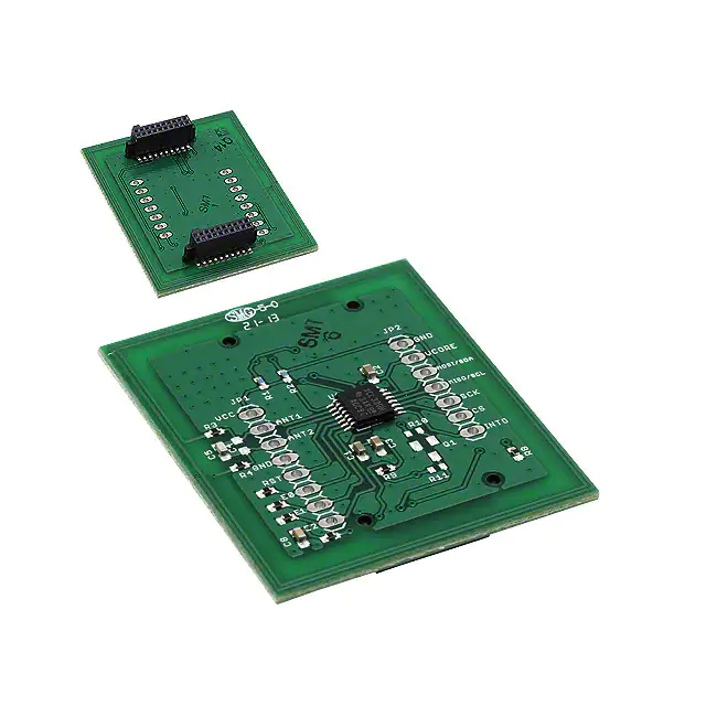


 工商网监
湘ICP备2023018690号
工商网监
湘ICP备2023018690号
