HDX RFID Reader System
Microreader RI-STU-MRD2
Reference Guide
Literature Number: SCBU049
August 2012
�Contents
1
2
3
Introduction ........................................................................................................................ 7
References ......................................................................................................................... 8
Definitions .......................................................................................................................... 8
4
Product Description
3.1
Abbreviations ............................................................................................................. 8
7
8
9
............................................................................................................ 9
4.1
Hardware SMD Module ............................................................................................... 10
4.2
Hardware DIL Module ................................................................................................. 12
4.3
Power Supply ........................................................................................................... 15
4.4
Synchronization ........................................................................................................ 15
4.5
Serial Port and USB Communication ............................................................................... 15
4.6
Handshake .............................................................................................................. 16
4.7
Trigger Mode ........................................................................................................... 16
4.8
Continuous Mode ...................................................................................................... 16
4.9
Demonstration Circuit ................................................................................................. 17
Antenna Construction ........................................................................................................ 18
5.1
Q-Factor ................................................................................................................. 18
5.2
Adapting the Inductance Range ..................................................................................... 19
Communication Between Host and Reader ........................................................................... 19
6.1
Legacy Microreader Protocol (LMP) ................................................................................. 20
6.2
Bit Sequence Protocol BSP .......................................................................................... 33
6.3
Easy Code Mode (ECM) .............................................................................................. 36
6.4
Setup Mode ............................................................................................................. 67
Operating Conditions ......................................................................................................... 99
Transponder Downlink Timings ........................................................................................... 99
External Power Reader Module (RFM) ................................................................................ 100
2
Table of Contents
5
6
SCBU049 – August 2012
Submit Documentation Feedback
Copyright © 2012, Texas Instruments Incorporated
�www.ti.com
List of Figures
1
RI-STU-MRD2 Module ..................................................................................................... 7
2
Overview ..................................................................................................................... 9
3
Top View With Pin Numbers of the Microreader 2 SMD Module
4
SMD Module Pin Configuration .......................................................................................... 11
5
Top, Front, and Side View Measurements of DIL Module ........................................................... 12
6
Microreader 2 Demonstration Circuit With USB Interface............................................................ 17
7
BCC Field Example ....................................................................................................... 20
8
LMP Command Byte Field 1 Example .................................................................................. 21
9
LMP Command Byte Field 2 Example .................................................................................. 21
10
BCC Field Example ....................................................................................................... 22
11
Read Only Command Format............................................................................................ 24
12
Read-Only Response Data Format ..................................................................................... 24
13
Programming Data Format of the 64-bit Read/Write Transponder ................................................. 25
14
General Read Data Formats of MPT Transponders .................................................................. 26
15
Programming Data Format of the MPT Transponders ............................................................... 27
16
Lock Page Data Format of MPT Transponder ......................................................................... 28
17
Response Data Format of MPT Transponder ......................................................................... 29
18
Data Format of the Selective Read Page .............................................................................. 30
19
Data Format of the Selective Program Page Function ............................................................... 31
20
Data Format of the Selective Lock Page Function .................................................................... 32
21
STAT Signal Mode ........................................................................................................ 92
...................................................
SCBU049 – August 2012
Submit Documentation Feedback
List of Figures
Copyright © 2012, Texas Instruments Incorporated
10
3
�www.ti.com
List of Tables
1
Mechanical Data of SMD Module ....................................................................................... 10
2
SMD Module Pin Functions .............................................................................................. 10
3
Mechanical Data of DIL Module ......................................................................................... 12
4
Pin Functions DIL Module ................................................................................................ 13
5
Antenna Parameters ...................................................................................................... 18
6
Transmit Stage Parameters .............................................................................................. 18
7
LMP Command Format (Full) ............................................................................................ 20
8
LMP Command Byte Field 1 Bit Format ................................................................................ 20
9
LMP Command Byte Field 2 Bit Format ................................................................................ 21
10
LMP Data Field Bit Format ............................................................................................... 22
11
LMP Command Response Format (Full) ............................................................................... 22
12
LMP Status Byte Bit Format
13
14
15
16
17
18
19
20
21
22
23
24
25
26
27
28
29
30
31
32
33
34
35
36
37
38
39
40
41
42
43
44
45
46
47
4
.............................................................................................
LMP Response Data Bit Format .........................................................................................
LMP Charge Only Read for Read-Only Transponder ................................................................
LMP Program Command Format for R/W Transponder..............................................................
General Read Page Command Format for MPT Transponder ......................................................
LMP Program Page Command Format for MPT Transponder ......................................................
LMP Command Format for Lock Page of MPT Transponder........................................................
LMP General Read Data Format of MPT 16/17 .......................................................................
LMP Program Page data Format of SAMPT Transponder ..........................................................
LMP Lock Page data Format of SAMPT Transponder ...............................................................
BSP Command Format (Full) ............................................................................................
Command Byte CMD1 ....................................................................................................
Command Byte CMD2 ....................................................................................................
CMD2 Downlink Timing Coding .........................................................................................
Command Byte CMD3 ....................................................................................................
Special TX Mode ..........................................................................................................
BSP Command Response Format ......................................................................................
Raw Data Bit Sequence ..................................................................................................
ECM Command Format ..................................................................................................
ECM Device Codes .......................................................................................................
ECM Command Codes Overview .......................................................................................
ECM Command Response Format .....................................................................................
Status Byte Definition for Host to Reader Protocol Status ...........................................................
Status Byte Definition for Reader to Transponder Protocol Status .................................................
Coding of Status Byte 2 ..................................................................................................
Device Commands Read Only Transponder ..........................................................................
ECM Charge only Read Command Format ............................................................................
Device Commands Read Write Transponder R/W ....................................................................
ECM Charge Only Read Command Format ...........................................................................
ECM Program Command Format for R/W .............................................................................
ECM Command Format Program(CRC Calc) Command Format for R/W .........................................
Device Commands Multipage Transponder MPT 16/17 .............................................................
ECM Charge Only Read Command Format for MPT .................................................................
ECM Read Page Command Format for MPT..........................................................................
ECM Program Page Command Format for MPT ......................................................................
ECM Program Page (CRC Calc) Command Format for MPT .......................................................
List of Tables
23
23
24
25
26
27
28
30
31
32
33
34
34
34
34
35
35
35
36
37
37
38
38
39
40
41
41
42
42
43
43
44
44
45
45
46
SCBU049 – August 2012
Submit Documentation Feedback
Copyright © 2012, Texas Instruments Incorporated
�www.ti.com
48
ECM Lock Page Command Format for MPT .......................................................................... 46
49
Device Commands for HDX+ Transponder ............................................................................ 47
50
ECM Charge Only Read Command Format for HDX+ ............................................................... 47
51
ECM Read UID Command Format for HDX+ .......................................................................... 48
52
ECM General Read Command Format for HDX+ ..................................................................... 48
53
ECM Selective Read Command Format for HDX+ ................................................................... 49
54
ECM Read Multi Block Command Format for HDX+ ................................................................. 49
55
ECM Selective Read Multi Block Command Format for HDX+
56
ECM Program Command Format for HDX+ ........................................................................... 50
57
ECM Selective Program Command Format for HDX+
58
ECM Program Multi Block Command Format for HDX+ ............................................................. 51
59
ECM Selective Program Multi Block Command Format for HDX+.................................................. 52
60
ECM Lock Block Command Format for HDX+
52
61
ECM Program Selective Lock Block Command Format for HDX+
53
62
63
64
65
66
67
68
69
70
71
72
73
74
75
76
77
78
79
80
81
82
83
84
85
86
87
88
89
90
91
92
93
94
95
96
.....................................................
...............................................................
........................................................................
.................................................
ECM Read Config Command Format for HDX+ ......................................................................
ECM Write Config Command Format for HDX+ .......................................................................
ECM Write AID Command Format for HDX+ ..........................................................................
ECM Program C-Trim Switches Command Format for HDX+.......................................................
ECM Stay Quiet Command Format for HDX+ .........................................................................
ECM Write TI R/W Command Format for HDX+ ......................................................................
Device Commands PaLFI ................................................................................................
ECM General Read Command Format for PaLFI .....................................................................
Byte Order of Response Data ...........................................................................................
ECM Selective Read Command Format for PaLFI ...................................................................
ECM Program Command Format for PaLFI ...........................................................................
ECM Program Command Format for PaLFI ...........................................................................
ECM Selective Program Command Format for PaLFI ...............................................................
ECM Selective Program Command Format for PaLFI ...............................................................
ECM Lock Command Format for PaLFI ................................................................................
ECM Selective Lock Command Format for PaLFI ....................................................................
ECM Protect Command Format for PaLFI .............................................................................
ECM Selective Protect Command Format for PaLFI .................................................................
ECM MSP Access Command Format for PaLFI ......................................................................
ECM Battery Check Command Format for PaLFI.....................................................................
ECM Battery Charge Command Format for PaLFI ...................................................................
Relation Between PaLFI Read Address and MRD2 Status Bytes ..................................................
Device Command Raw Data Response ................................................................................
ECM Raw Data Response Command Format ........................................................................
Raw Data Bit Sequence ..................................................................................................
Setup Mode Command Byte 2...........................................................................................
Setup Command Format .................................................................................................
Setup Command Response Format ....................................................................................
Setup Get Firmware Version Command Format ......................................................................
Setup Get Protocol Version Command Format .......................................................................
Setup Get Hardware Type Command Format .........................................................................
Setup Get Serial Number Command Format ..........................................................................
Setup Get PWM Timing Command Format ............................................................................
Setup Set PWM Timing Command Format ............................................................................
Setup Get PWM Timing Command Format ............................................................................
SCBU049 – August 2012
Submit Documentation Feedback
List of Tables
Copyright © 2012, Texas Instruments Incorporated
50
51
53
54
54
55
55
56
57
57
57
58
58
59
59
60
60
61
61
62
62
63
63
64
66
66
67
67
68
69
69
70
71
71
72
73
74
5
�www.ti.com
97
Setup Set PWM Timing Command Format ............................................................................ 75
98
Get PPM Timing Command Format
99
Set PPM Timing Command Format ..................................................................................... 77
100
Setup Get BLC Timing Command Format ............................................................................. 78
101
Setup Set BLC Timing Command Format
102
Setup Get BLC (Automotive) Timing Command Format ............................................................. 80
103
Set BLC (Automotive) Timing Command Format ..................................................................... 81
104
Setup Set Duration Power Burst 1 Command Format................................................................ 82
105
Setup Get Duration Power Burst 1 Command Format ............................................................... 82
106
Setup Set Duration Power Burst 2 Command Format................................................................ 83
107
Setup Get Duration Power Burst 2 Command Format ............................................................... 83
108
Set Downlink CRC Command Format .................................................................................. 84
109
Setup Set Uplink CRC Command Format
84
110
Set or Check R/W Data CRC Command Format
85
111
112
113
114
115
116
117
118
119
120
121
122
123
124
125
126
127
128
129
130
131
132
133
134
135
6
....................................................................................
.............................................................................
.............................................................................
.....................................................................
Setup Check MPT CRC Command Format ............................................................................
Setup Start 1-Slot Inventory Process Command Format ............................................................
Set Serial Port Com Speed Command Format ........................................................................
Speed Byte Data Format .................................................................................................
Setup Get Last Measured Low Bit Freq Command Format .........................................................
Setup Execute C-Trim Command Format ..............................................................................
Device Code Values ......................................................................................................
Status Byte .................................................................................................................
Carrier On or Off Command Format ....................................................................................
OKT Signal Timing Command Format ..................................................................................
Setup STAT Signal Mode Command Format ..........................................................................
Setup Get Status of SIG_IN_0 Command Format ....................................................................
Setup Get Status of SIG_IN_1 Command Format ....................................................................
Setup Set Status of SIG_OUT_0 Command Format .................................................................
Setup Set Status of SIG_OUT_1 Command Format .................................................................
Setup Set Demodulation Threshold Mode Command Format .......................................................
Setup Set External Power Reader Command Format ................................................................
Setup save Setting to Flash Command Format .......................................................................
Status Bit ...................................................................................................................
Setup Restore Settings to Factory Default Command Format ......................................................
Status Bit ...................................................................................................................
Operating Conditions......................................................................................................
Transponder Downlink Timings ..........................................................................................
Default Power Burst Values ..............................................................................................
Microreader RFM Connections .........................................................................................
List of Tables
76
79
86
87
88
88
89
90
90
90
91
91
92
93
93
94
94
95
96
97
97
98
98
99
99
99
100
SCBU049 – August 2012
Submit Documentation Feedback
Copyright © 2012, Texas Instruments Incorporated
�Reference Guide
SCBU049 – August 2012
Microreader RI-STU-MRD2
WARNING
The terminals across the antenna connectors ANT1 and ANT2
operate at potentially hazardous voltages. Effective safety
application procedures and knowledge are required to minimize
risk of electrical shock hazard when using this EVM. The user
should be technically qualified to operate this EVM, including
having full knowledge of risks associated in working with
electrically live and hazardous voltages commonly found in
development platforms. Careful review of General Texas Instruments
High Voltage Evaluation Module (TI HV EVM) User Safety Guidelines at
the end of this document is required prior to using this EVM.
1
Introduction
The Microreader RI-STU-MRD2 is a reader module with advanced features that is backward compatible
with the RI-STU-MRD1 module. It features new protocols and commands to communicate with TI lowfrequency (LF) half-duplex (HDX), and advanced transponders for programming and tuning after the
production phase. In addition to the DIL module size, which is compatible with the RI-STU-MRD1, the
reader is also available in a smaller SMD module RI-SMD-MRD2. Both modules can be used as direct
drop-in replacements for the RI-STU-MRD1.
This document describes the hardware and communication protocols of the RI-STU-MRD2 module.
Figure 1. RI-STU-MRD2 Module
SCBU049 – August 2012
Submit Documentation Feedback
Microreader RI-STU-MRD2
Copyright © 2012, Texas Instruments Incorporated
7
�References
2
www.ti.com
References
1.
2.
3.
4.
5.
2000 Reader System: Microreader RI-STU-MRD1 Reference Guide (SCBU027)
Reference Guide for 32-mm Glass Transponder (Read Only, Read/Write) (SCBU019)
Multipage, Selective Addressable and Selective Addressable (Secured) Transponders (SCBU020)
TMS37157 PaLFI data sheet (SWRS083)
ISO/IEC 18000-2:2004, Information technology – Radio frequency identification for item Management –
Part 2: Parameters for air interface communications below 135 kHz
6. ISO 14223-1:2003, Radio frequency identification of animals – Advanced transponders – Part 1: Air
interface
7. ISO 14223-2:2010, Radio frequency identification of animals – Advanced transponders – Part 2: Code
and command structure
3
Definitions
3.1
Abbreviations
AID: Animal Identification Code
PaLFI: Passive Low Frequency Interface
BCC: Block Check Character
PCB: Printed Circuit Board
BLC: Bit Length Coding
PPM: Pulse Position Modulation
BSP: Bit Sequence Protocol
PWM: Pulse Width Modulation
CDC: Communication Device Class
DIL: Dual in Line
RFU: Reserved for Future Use
ECM: Easy Code Mode
RO: Read Only (Transponder)
EOF: End of Frame
R/W: Read/Write (Transponder)
FBCC: Frame Block Check Character
FSK: Frequency Shift Keying
RX: Receive
SM: Setup Mode
HDX: Half Duplex
SMD: Surface Mounted Device
HDX+: Half Duplex Plus
SOF: Start of Frame
LMP: Legacy Microreader Protocol
MCU: Micro Controller Unit
TX: Transmit
WLSC: Wireless Synchronization
MPT: Multipage Transponder
SCI: Serial Communication Interface
MRD1: Microreader 1 (RI-STU-MRD1)
8
RFM: Radio Frequency Power Module
SMPS: Switched-Mode Power Supply
Microreader RI-STU-MRD2
SCBU049 – August 2012
Submit Documentation Feedback
Copyright © 2012, Texas Instruments Incorporated
�Product Description
www.ti.com
4
Product Description
The Microreader module is available as a dual in line (DIL) module or a surface-mount device (SMD)
module that can be plugged into or soldered onto an application-specific adapter board. The Microreader
supports serial and USB data communications between a PC and TI transponders. The Microreader
supports TTL data communications through its serial communications interface (SCI), which allows
communication to a standard interface when using an additional communications driver (for example,
RS232 or RS422). In addition, a USB interface is available and requires only a few external components.
For easy access to the USB port from the PC side, the reader is managed as a COM port.
The Microreader can be controlled remotely either by providing certain inputs with the corresponding
voltage level or by sending commands to the SCI or USB. The Microreader can be driven either with or
without synchronization. Synchronization can be either wireless or wired to enable reliable operation in
multi-reader environments. Two outputs show the reader status and inform the user about a successful
command execution. The Microreader supports all available TI LF HDX transponders.
The supply voltage can vary between 2.7 V and 5.5 V. A voltage regulator and level shifters are
implemented to maintain the specified supply range.
A microcontroller generates the transmit signal, demodulates the receive signal, and manages the two
host interfaces.
2.7 V to 5.5 V
USB
Antenna
47 µH
Serial Port
Microreader 2
Module
Control
Status
Figure 2. Overview
SCBU049 – August 2012
Submit Documentation Feedback
Microreader RI-STU-MRD2
Copyright © 2012, Texas Instruments Incorporated
9
�Product Description
4.1
www.ti.com
Hardware SMD Module
The following sections describe the SMD module hardware and pin functions.
4.1.1
SMD Module Product Dimensions
Figure 3 shows the SMD module with single-sided component placement, and Table 1 shows the product
dimensions. The size and shape of the pads are designed to make assembly and soldering of the module
in an automated production process as easy as possible.
22.95 mm (max)
27
26
25
24
23
22
21
20
19
18
28
17
29
16
30
15
2.54 mm grid
31
14
32
13
33
12
34
11
1
2
3
4
5
6
7
8
9
10
28.05 mm (max)
Figure 3. Top View With Pin Numbers of the Microreader 2 SMD Module
Table 1. Mechanical Data of SMD Module
Parameter
Min
Typ
Max
Unit
Length
27.8
27.9
28.05
mm
Width
22.7
22.8
22.95
mm
Height
3.0
3.5
mm
Weight
4.1.2
2.0
g
SMD Module Pin Functions
Table 2. SMD Module Pin Functions
(1)
10
Pin
Pin Name
Function (1)
1
SYNC
O
Output for wired synchronization (yellow LED)
2
RDEN-
I
Input for wired synchronization and single read trigger
3
RESET-
I
Reset of the Microreader
4
RXD
I
Receive data signal input of serial interface
5
TXD
O
Transmit data signal output of serial interface
6
GND
P
Do not connect
7
GND
8
3_3V_OUT
9
Reserved
Description
10
Reserved
O
11
SIG_OUT_0
O
Programmable signal output 0
12
SIG_OUT_1
O
Programmable signal output 1 or TXCT- in RFM mode
B = Bidirectional, I = Input, O = Output, P = Power
Microreader RI-STU-MRD2
SCBU049 – August 2012
Submit Documentation Feedback
Copyright © 2012, Texas Instruments Incorporated
�Product Description
www.ti.com
Table 2. SMD Module Pin Functions (continued)
4.1.3
13
GND
14
SIG_IN_0
I
Programmable signal input 0 or RXDT in RFM mode
15
SIG_IN_1
I
Programmable signal input 1 or RXCK in RFM mode
16
Reserved
17
Reserved
18
ANT1
19
ANTCAP
20
ANT2
Antenna terminal 2
21
GNDP
Ground for output stage
22
VSP
P
Supply voltage output stage
23
VSL
P
Supply voltage for logic
24
CRDM
I
Input for continuous read mode
25
WLS
I
Input to turn wireless synchronization on
26
OKT
O
Read of valid transponder ID (green LED)
27
STAT
O
Status of RF transmitter control (red LED) (see Section 6.4.3.31)
28
USB_VBUS
P
+5 V from USB port
29
USB_D-
B
USB data
30
USB_D+
B
USB data
31
GND
32
USB_PUR
O
USB pullup resistor
33
Reserved
34
Reserved
Antenna terminal 1
Antenna capacitor terminal
SMD Module Pin Configuration
STAT
OKT
WLS
CRDM
VSL
VSP
GNDP
ANT2
ANTCAP
ANT1
Figure 4 shows the pin configuration of the SMD module.
27
26
25
24
23
22
21
20
19
18
30
15
SIG_IN_1
GND
31
14
SIG_IN_0
USB_PUR
32
13
GND
RST
33
12
SIG_OUT_1
reserved
34
11
SIG_OUT_0
SYNC
1
2
3
4
5
6
7
8
9
10
LF_RX
USB_D+
reserved
reserved
3_3V_OUT
16
GND
29
GND
USB_D-
TXD
reserved
RXD
17
RESET-
28
RDEN-
VBUS
Figure 4. SMD Module Pin Configuration
SCBU049 – August 2012
Submit Documentation Feedback
Microreader RI-STU-MRD2
Copyright © 2012, Texas Instruments Incorporated
11
�Product Description
4.2
www.ti.com
Hardware DIL Module
The following sections describe the DIL module hardware and pin functions.
4.2.1
Product Dimensions
Figure 5 and Table 3 show the layout and dimensions of the DIL module.
38.7mm
16
1
15
6mm
12mm
25.4mm
29.6mm
30
14 Pitches 2.54mm
Note: Pin size: 0.64 x 0.64 mm
Note: Contact plating: Gold
Note: Recommended pin hole size diameter: 1 mm
Figure 5. Top, Front, and Side View Measurements of DIL Module
Table 3. Mechanical Data of DIL Module
Parameter
Min
Typ
Max
Unit
Length
37.9
38.3
38.7
mm
Width
28.8
29.3
29.6
mm
Height including pins
11.5
12
12.5
mm
Weight
12
5.0
Microreader RI-STU-MRD2
g
SCBU049 – August 2012
Submit Documentation Feedback
Copyright © 2012, Texas Instruments Incorporated
�Product Description
www.ti.com
4.2.2
DIL Module Pin Functions
Table 4. Pin Functions DIL Module
(1)
4.2.3
Pin
Pin Name
Function (1)
1
SYNC
O
Output for wired synchronization (yellow LED)
2
RDEN-
I
Input for wired synchronization and single read trigger
3
Reserved
4
RESET-
5
6
Description
Do not connect
I
Reset of the Microreader
RXD
I
Receive data signal input of serial interface
TXD
O
Transmit data signal output of serial interface
7
USB_D-
B
USB data
8
USB_D+
B
USB data
P
Do not connect
9
3_3V_OUT
10
Reserved
11
SIG_OUT_0
O
Programmable signal output 0
12
SIG_OUT_1
O
Programmable signal output 1 or TXCT- in RFM mode
13
SIG_IN_0
I
Programmable signal input 0 or RXDT in RFM mode
14
SIG_IN_1
I
Programmable signal input 1 or RXCK in RFM mode
Do not connect
15
GND
16
ANT1
17
ANTCAP
Antenna capacitor terminal
18
Reserved
Do not connect
19
ANT2
20
Reserved
21
GNDP
Antenna terminal 1
Antenna terminal 2
Do not connect
Ground for output stage
22
VSP
P
Supply voltage output stage
23
USB_PUR
O
USB pullup resistor
24
VSL
P
Supply voltage logic
25
GND
26
CRDM
I
Ground for logic
Input for continuous read mode
27
WLS
I
Input to turn wireless synchronization on
28
USB_VBUS
P
+5 V from USB port
29
OKT
O
Read of valid transponder ID (green LED)
30
STAT
O
Status of RF transmitter control (red LED)
B = Bidirectional, I = Input, O = Output, P = Power
DIL Module Pin Functional Description
SYNC (1)
Output for wired synchronization. This output is at GND level until the Microreader starts its read cycle,
at which time it goes to VSL until the read, program, or lock cycle is finished.
RDEN- (2)
Input for wired synchronization. Pull this pin to VSL to prevent the Microreader output stage from
transmitting. Pull this pin to GND to enable transmitting. The Microreader samples this input at the start
of its own read, program, or lock cycle; therefore, if the input goes to VSL after a cycle is started, the
cycle is not interrupted. RDEN- is a high-impedance input and must be tied to GND via a suitable
resistor (27 kΩ) when not in use.
To trigger a single read when the Microreader is idle, pull the RDEN- pin logic high for 100 µs. The
single read starts on the falling edge of the 100-µs pulse.
SCBU049 – August 2012
Submit Documentation Feedback
Microreader RI-STU-MRD2
Copyright © 2012, Texas Instruments Incorporated
13
�Product Description
www.ti.com
RESET- (4)
Pull this pin to GND to hold the Microreader in reset. If the reset pin is not used, it can be left
disconnected (it is internally pulled up). Minimum pulse duration to perform a reset is 1 ms. After a
reset, the processor requires between 28 ms and 132 ms (typically 72 ms) before it can receive new
instructions via the serial communications interface.
RXD (5)
Input configured to receive serial data at 9600 Baud (default, configurable up to 115k Baud), 1 start bit,
8 data bits, no parity, and 1 stop bit.
TXD (6)
Output configured to transmit serial data at 9600 Baud (default, configurable up to 115k Baud), 1 start
bit, 8 data bits, no parity, and 1 stop bit.
USB_D-, USB_D+ (7, 8)
USB data transmit and receive
USB_VBUS (28)
USB power voltage
GND (15, 25)
Pins 15 and 25 are ground for the logic part.
ANT1 (16)
Antenna pin for the connection of a 47-µH low-Q antenna.
ANTCAP (17)
To use an antenna of lower inductance, connect a suitable capacitor between ANT1 and ANTCAP.
This additional capacitor (ceramic, 100 VDC) is in parallel with the 30-nF resonance capacitor on the
Microreader.
ANT2 (19)
Antenna pin (GND) for the connection of a 47-µH low-Q antenna.
GNDP (21)
Ground for the output stage.
VSP (22)
Positive supply voltage (2.7 V to 5.5 V, same as VSL) for the output stage.
VSL (24)
Positive supply voltage (2.7 V to 5.5 V, same as VSP) for the logic part.
CRDM (26)
Apply a logic high signal to run the Microreader in a continuous charge-only read mode. When the
CRDM pin is logic low, the Microreader is in an idle state waiting for commands via the serial interface
or for a trigger signal (RDEN-) to start a single read out cycle. CRDM is a high-impedance input and
must be tied to either VSL or GND via a suitable resistor (27 kΩ).
WLSC (27)
Enables or disables wireless synchronization. To enable the wireless synchronization, pin 27 must be
pulled to VSL. When wireless synchronization is enabled, the Microreader tries to synchronize its
transmit signals with any other readers in range. To disable wireless synchronization, pull pin 27 to
GND. Pin 27 is a high-impedance input and must be tied to either VSL or GND via a suitable resistor
(27 kΩ). Wireless synchronization can also be turned on or off by a command on the serial interface.
This command has priority over the WLSC input.
OKT (29)
This output is set to logic high for approximately 60 ms if a valid transponder was read. It can be
connected externally to an LED to indicate the result of the read cycle (see Section 6.4.3.30).
14
Microreader RI-STU-MRD2
SCBU049 – August 2012
Submit Documentation Feedback
Copyright © 2012, Texas Instruments Incorporated
�Product Description
www.ti.com
STAT (30)
Pin 30 is set to logic low when the RF transmitter is activated. Supplying an external LED with this
signal makes the status of the Microreader visible (see Section 6.4.3.31).
4.3
Power Supply
There are two separate (2.7 V to 5.5 V) supplies to the Microreader, one for the output stage (VSP) and
the other for the logic (VSL). Both supplies, VSP and VSL, must have the same voltage. On power up,
VSL should rise faster than 0.1 V/ms to ensure reliable operation.
To avoid problems with noise conducted by the supply lines if a single supply is used, use separate
connections from a common decoupling capacitor to the Microreader.
NOTE: The RF module must not be supplied by most switched mode power supplies (SMPS). This
is because most SMPS operate at frequencies near 50 kHz. The harmonics of the generated
field can interfere with the receiver. Therefore, use linear regulated power supplies. An
SMPS with a fundamental operating frequency of 200 kHz or higher can be used.
4.4
Synchronization
There are two possible methods of wired synchronization:
• Connect a pulse waveform to all RDEN- input pins of the Microreaders to be synchronized. Hold the
pulse at VSL and drop it to GND for 100 µs every 200 ms.
• Connect all SYNC outputs to an OR gate and then connect the output of the OR gate as an input to
the RDEN- of each Microreader to be synchronized.
Wireless synchronization of the Microreader is very effective at synchronizing to adjacent readers;
however, problems can occur if the antennas are positioned so that a transponder is within range of two
readers at the same time. In this situation, one reader could synchronize with the transponder instead of
with the other reader.
When the WLSC input is active, the Microreader is in wireless synchronization mode. Wireless
synchronization can also be turned on or off by a corresponding command via the serial interface. During
execution of this command, it has priority over the WLSC input. After the command execution, the status
of the WLSC input is considered again.
NOTE: It is not recommended to have both wired and wireless synchronization on, because the
synchronization could be unreliable. It is recommended to use bus drivers for wired
synchronization with other Microreaders and to prevent ESD damage. Wired or wireless
synchronization prolongs the cycle time by 20 ms (typical).
4.5
Serial Port and USB Communication
Communication between host and reader is done by either the serial port or the USB port. Both ports can
accept commands. No setup or switch between these ports is necessary. Each response is sent to the
port from which the command was received. If the CRDM pin is active, the response is sent to the serial
port, but when a USB connection is established the response is sent to the USB port.
The factory default for both interfaces is 9600 Baud, 1 start bit, 8 data bits, no parity, and 1 stop bit; they
can be connected directly to a communications driver to allow a half duplex communication with a PC via
its serial communications interface (for example: RS232 or RS422)or USB Interface.
See Section 6 for details on the communication protocols.
SCBU049 – August 2012
Submit Documentation Feedback
Microreader RI-STU-MRD2
Copyright © 2012, Texas Instruments Incorporated
15
�Product Description
4.6
www.ti.com
Handshake
The Microreader accepts handshake commands Xon and Xoff. When it receives an Xoff (0x13) the
Microreader stops its current operation and stops transmitting data via the serial port. It stays in idle mode
until Xon (0x11) is received when it continues with the previous mode or command. During this idle period,
the Microreader accepts commands via the serial port, however, it waits for its execution until Xon is
received. In this idle period, the Microreader can store only one command.
NOTE: While receiving a command protocol from the serial port, Xon or Xoff is interpreted as normal
data without affecting the serial communication.
4.7
Trigger Mode
When the Microreader is in idle mode, it is possible to trigger a single charge-only read with a power burst
duration of 50 ms by taking the RDEN- pin to logic high for 100 µs. The single read starts on the falling
edge of the 100-µs pulse.
If a transponder command is sent to the Microreader via the SCI while RDEN- is in a logic high state
(waiting position), a falling edge on RDEN- triggers execution of the command. In waiting position the
Microreader can only store one command. This means that if two commands were to be sent to the
Microreader while it is in the waiting position, the second command overwrites the first one.
4.8
Continuous Mode
When the CRDM input is active, the Microreader enters a continuous charge-only read mode using power
burst duration of 50 ms. The serial data input takes priority over the CRDM input such that if a serial
command is received, it is executed regardless of the state of the CRDM input. After the execution of the
serial data command, the Microreader continues with the previous read mode.
In the default continuous read mode, only those valid RO, R/W, or MPT IDs that differ from the previously
read ID, or valid IDs read after a NO READ, are transferred via the SCI (Normal Mode). The Microreader
can be set to transfer all valid IDs that are read (Line Mode) by means of a corresponding serial data
command.
Without synchronization the Microreader has a reading frequency of approximately ten readouts per
second using power burst duration of 50 ms.
16
Microreader RI-STU-MRD2
SCBU049 – August 2012
Submit Documentation Feedback
Copyright © 2012, Texas Instruments Incorporated
�Product Description
www.ti.com
4.9
Demonstration Circuit
Figure 6 shows a demonstration circuit. Pin numbers are shown for the DIL module.
Figure 6. Microreader 2 Demonstration Circuit With USB Interface
SCBU049 – August 2012
Submit Documentation Feedback
Microreader RI-STU-MRD2
Copyright © 2012, Texas Instruments Incorporated
17
�Antenna Construction
5
www.ti.com
Antenna Construction
The Microreader has been designed for use with a 47-µH antenna with a Q of 10 to 20 to generate the
exciter frequency of 134.2 kHz. Because of the low Q, the system does not need to be tuned.
Table 5 shows the typical parameters for a circular air coil antenna.
Table 5. Antenna Parameters
Inner diameter of transmit antenna
A
75
mm
Outer diameter of transmit antenna
B
78
mm
Radius of transmit antenna
rtx
0.03825
m
Inductance
Ltx
47
µH
Turns
Ntx
15
Diameter of wire
dw
0.2
Antenna quality factor (134.2 kHz)
Qant
16
Antenna resistance (134.2 kHz)
Rant
2.5
mm
Ω
Table 6 shows the Microreader 2 transmitter stage parameters.
Table 6. Transmit Stage Parameters
Supply voltage
Bridge drain-source resistance
5.1
Usup
2.7 - 5.5
V
RonPx, RonNx
0.25, 0.1
Ω
Damping resistor
Rdmp
2
kΩ
Resonance capacitor
Cres
30
nF
Q-Factor
If the antenna's Q factor exceeds 20:
• The output capacitors are overloaded and long-term damage could result.
• The antenna may still be resonating when the response from the transponder is received. Without
built-in damping, the data may not be correctly received.
• The antenna may be detuned if there is any metal in the area.
The following formula provides a method of calculating the approximate Q factor of the antenna:
Q=
2πfL
R
(1)
Where,
f = 134200 Hz (Frequency = 134.2 kHz)
L = Inductance (H)
R = Series resistance (Ω)
Equation 2 shows an example for:
Inductance (L) = 47 µH
Resistance (R) = 2.2 Ω
Q=
=
2 × π × 134200 × 0.000047
2.2
39.636
2.2
(2)
= 18
18
Microreader RI-STU-MRD2
SCBU049 – August 2012
Submit Documentation Feedback
Copyright © 2012, Texas Instruments Incorporated
�Communication Between Host and Reader
www.ti.com
5.2
Adapting the Inductance Range
If the antenna is outside of the required inductance range of 46 to 48 µH, adapt it to work with the
Microreader by adding an external capacitor to it, either in series or in parallel. This external capacitor can
change the inductance range by 5 µH.
Equation 3 shows the formula to calculate the total resonance capacity.
Ctot =
1
2
4π L Ant f 2
(3)
If the antenna inductance is less than 46.1 µH, add an extra capacitor (externally) to the antenna between
pin ANT1 and pin ANTCAP. Equation 4 shows the formula for the value of this capacitor.
Cext = Ctot – 30 nF
(4)
If the antenna inductance is more than 47.9 µH, add an extra capacitor in series with the antenna between
pin ANT2 and the antenna. Equation 5 shows the formula for the value of this capacitor.
1
1
1
=
–
Cext
Ctot
30 nF
6
(5)
Communication Between Host and Reader
Communication between host and reader is done either by the serial port or the USB port. Both ports can
accept commands. No setup or switch between these ports is necessary. Response is sent to the port
from which the command was received.
The USB port is configured as CDC (Communication Device Class). If connected to a PC, no special
driver is required, but an INF file is required, which can be downloaded from the Microreader product
folder on the TI web page. If the port is installed by the host, it is accessible as COM port.
Data transfer is done in a binary format. No ASCII characters interpretation is done. Therefore, the use of
the ASCII carriage return (CR) or line feed (LF) for the command termination is not possible. The reader
assumes a command as terminated if the number of bytes specified after the 0x01 start byte is received,
or if no new byte is received for 10 ms.
The Microreader can process different communication protocols:
It can interpret the protocol defined for the previous Microreader RI-STU-MRD1 with no restrictions. This
protocol is referred to as Legacy Microreader Protocol (LMP).
Based on this protocol, expansions are defined to support new functionality. These expansions are:
• Bit Sequence Protocol (BSP) allows specification of a transponder downlink at bit level.
• Easy Code Mode (ECM) Protocol allows specification of a transponder downlink with a minimum of
parameters based on the specification of the device that is in use and the associated command.
• Setup Mode Protocol (SM) is used to set up reader parameters or to manage functionality such as the
inventory process.
NOTE: It is recommended that all users take advantage of the Easy Code Mode (ECM) Protocol
when possible. The use of the Legacy Microreader Protocol (LMP) should be restricted to
users who migrate from the RI-STU-MRD1 module and have software already available. For
special purposes, when the user wants do define a transponder protocol at bit level, the Bit
Sequence Protocol (BSP) can be used.
SCBU049 – August 2012
Submit Documentation Feedback
Microreader RI-STU-MRD2
Copyright © 2012, Texas Instruments Incorporated
19
�Communication Between Host and Reader
6.1
www.ti.com
Legacy Microreader Protocol (LMP)
6.1.1
LMP Command Format
Table 7 shows the LMP command format.
Table 7. LMP Command Format (Full)
•
•
•
•
•
•
Start Byte
Length
CMD1
CMD2
(optional)
Data Field
(1...)
Data Field
(N)
BCC
Byte 0
Byte 1
Byte 2
Byte 3
Byte 4 (3)...
Byte ...n+3 (2)
Byte n+4 (3)
0x01
0xyy
0xyy
0xyy
0xyy
0xyy....
calculated
The Start Byte has a fixed value of 0x01 and marks the beginning of the command.
The Length byte indicates the length in bytes of the following command and data fields.
CMD1 command code description is in Section 6.1.1.1.
CMD2 is the optional command code; description is in Section 6.1.1.1.
The presence of the Data Field is optional; whether or not it is included and the number of bytes
depend on the command codes. This is described in Section 6.1.1.2.
The BCC Field is a one-byte value of the Longitudinal Redundancy Check calculation (XORed bytes)
for the preceding message. The calculation is performed on the whole command excluding the Start
Byte.
Example: 02 08 32
02
0000 0010
08
0000 1000
XOR 0000 1010
32
0011 0010
XOR 0011 1000 = 38h
Figure 7. BCC Field Example
NOTE: The total number of bytes sent within a protocol frame (including Start Mark and BCC) is
limited to 41 bytes.
6.1.1.1
LMP Command Codes
The Command Fields define the mode in which the Microreader operates and determines the operation
that is to be carried out in the transponder. The value of the Command Codes determine whether or not
information specified in the Data Fields is sent to the transponder.
Table 8. LMP Command Byte Field 1 Bit Format
Command
Field (1) Bit
Use
Setting
Comment
00 (MSB, LSB) Perform single command (for example: single read, program, lock)
01
Read in continuous Normal Mode
10
Read in continuous Line Mode
11
Send Microreader S/W version
FBCC Calculation
1/0
If set, Microreader calculates FBCC of the MPT protocol
3
Power Burst I
1/0
If set, needs to be determined in Data Field (see Section 6.1.1.2)
4
Power Pause Duration
1/0
If set, needs to be determined in Data Field
5
Power Burst II
1/0
If set, needs to be determined in Data Field
6
Data
1/0
If set, needs to be determined in Data Field
7
Cmd Expansion Field
1/0
If set, Command Field (2) follows
0, 1
2
20
Mode, Command
Microreader RI-STU-MRD2
SCBU049 – August 2012
Submit Documentation Feedback
Copyright © 2012, Texas Instruments Incorporated
�Communication Between Host and Reader
www.ti.com
If bit 5 (Power Burst II; for example, for programming and locking) is set, the Microreader automatically
operates in single read mode. Thus the application can validate the programming or lock response before
a further cycle is started.
If bit 2 (FBCC calculation) and bit 6 (Data) are set, the Microreader automatically calculates a two byte
BCC over the data to be sent to the transponder and adds it to the protocol. When bits 2 and 6 are set,
the PC must not send the 2 byte FBCC to the Microreader.
Bit 4 (Power Pause Duration) is for future use and must not be set when addressing standard
transponders.
Example: E8h = 1110 1000b
1110 1000
Perform single command
No FBCC calculation
Power burst I value set in Data Field
Default Set to 0
Power burst II value set in Data Field
Data values follows in Data Field
Command Field (2) follows
Figure 8. LMP Command Byte Field 1 Example
Table 9. LMP Command Byte Field 2 Bit Format
Bit
Use
Setting
0
Special Write Timing
1 or 0
If set, needs to be determined in Data Field
Comment
1
Wireless Synchronization
1 or 0
If set, wireless synchronization is used
2
DBCC calculation
1 or 0
If set, Microreader calculates DBCC of the R/W and MPT write data
3-7
Reserved
Example: 06h = 0000 0110b
0000 0110
No special write timing
Wireless synchronization used
Microreader calculates DBCC
Bits 3-7 reserved
Figure 9. LMP Command Byte Field 2 Example
If Command Field (2) is not present, standard write timings are used and wireless synchronization is
turned on or off according to the status of input line WLSC.
NOTE: The settings specified in Command Field (1) and (2) are only valid during the execution of
the current command.
SCBU049 – August 2012
Submit Documentation Feedback
Microreader RI-STU-MRD2
Copyright © 2012, Texas Instruments Incorporated
21
�Communication Between Host and Reader
6.1.1.2
www.ti.com
LMP Data Field
The presence of the data field depends on the setting of the Command Field.
If a command bit that requires the data field is set to 1 (for example, Command bit 3 "Power Burst I"), then
Data Field 1 is present defining the Power Burst length. If the relevant bit in the Command Field is set to 0
the consequent Data Field is omitted, this results in the following data field being moved forward
(decremented) by one.
Table 10. LMP Data Field Bit Format
(1)
Data Field
Use
Range (dec)
Comment
1
Power Burst I
1 to 255 (ms)
If bit 3 of Command Field(1) is set
2
Power Pause Duration
1 to 255 (ms)
If bit 4 of Command Field(1) is set
3
Power Burst II
1 to 255 (ms)
If bit 5 of Command Field(1) is set
4/5
Toff Low (LSByte/MSByte)
28 to 2044 (ms)
If bit 0 of Command Field(2) is set
6/7
Ton Low (LSByte/MSByte)
28 to 2044 (ms)
If bit 0 of Command Field(2) is set
8/9
Toff High (LSByte/MSByte)
28 to 2044 (ms)
If bit 0 of Command Field(2) is set
10/11
Ton High (LSByte/MSByte)
28 to 2044 (ms)
If bit 0 of Command Field(2) is set
12
# of Data Fields that follow
13...
Data Fields
See
(1)
If bit 6 of Command Field(1) is set
LSByte first
The number of Data Fields must not cause an infringement of the total number of bytes allowed within a protocol frame.
Transponder command protocols are described in detail in Section 6.1.3.
6.1.2
LMP Command Response Format
Table 11. LMP Command Response Format (Full)
•
•
•
•
•
Start Byte
Length
Status
Data
BCC
Byte 0
Byte 1
Byte 2
Byte 4...n
Byte n + 1
0x01
0xyy
0xyy
0xyy...
calculated
The Start Byte has a fixed value of 0x01 and marks the beginning of the command.
The Length byte indicates the length in bytes of the following command and data fields.
Status description is in Section 6.1.2.1.
The Response Data Format is described in Section 6.1.2.2.
The BCC Field is a one-byte value of the Longitudinal Redundancy Check calculation (XORed bytes)
for the preceding message. The calculation is performed on the whole command excluding the Start
Byte.
Example: 02 08 32
02
0000 0010
08
0000 1000
XOR 0000 1010
32
0011 0010
XOR 0011 1000 = 38h
Figure 10. BCC Field Example
22
Microreader RI-STU-MRD2
SCBU049 – August 2012
Submit Documentation Feedback
Copyright © 2012, Texas Instruments Incorporated
�Communication Between Host and Reader
www.ti.com
6.1.2.1
Status Byte Format
The Status byte provides feedback from the preceding read or program operation (see Table 12).
Table 12. LMP Status Byte Bit Format
Status Bits
Setting
Transponder type: RO
01
Transponder type: R/W
10
Transponder type: MPT/SAMPT
11
Other
0, 1
6.1.2.2
Comment
00 (MSB, LSB)
2
1 or 0
If set, Start byte detected
3
1 or 0
If set, DBCC OK
4
1 or 0
If set, FBCC OK
5
1 or 0
If set, Microreader S/W version follows
6–7
Reserved
Response Data Format
Table 13. LMP Response Data Bit Format
Type
Bytes in Data Field
RO
8
Identification Data (LSByte first), see Section 6.1.3
Comment
R/W
8
Identification Data (LSByte first)), see Section 6.1.4
MPT, SAMP
9
Identification Data (LSByte first), plus Read Address, see Section 6.1.5 and
Section 6.1.6
Other
14
Complete transponder protocol without pre-bits provided that a valid RO or R/W start
byte was detected
No read
0
No Data Fields, not even transponder start byte was detected, status 0x03
Software version
1
For example: 0x15 indicates software version 1.5
SCBU049 – August 2012
Submit Documentation Feedback
Microreader RI-STU-MRD2
Copyright © 2012, Texas Instruments Incorporated
23
�Communication Between Host and Reader
6.1.3
www.ti.com
Device Commands Read-Only Transponder RO
6.1.3.1
Charge Only Read
Rea- only transponders support a command called Charge Only Read. The response data contain a 16-bit
checksum and a 64-bit ID.
OFF
RF Transmitter
Power Burst
Read
50 ms
20 ms
ON
Figure 11. Read Only Command Format
Table 14. LMP Charge Only Read for Read-Only Transponder
Charge Only Read
Command
Length
(Bytes)
Byte Number
Start Byte
1
0
01
hex
Length
1
1
02
hex
CMD (Power Burst 1 + Single Command)
1
2
08
hex
Data Field(Power Burst1 with 50 ms Duration)
1
3
32
hex
BCC
1
4
38
hex
Length
(Bytes)
Byte Number
Start Byte
1
0
01
hex
Length
1
1
09
hex
Status (Valid RO, Start byte detected, DBCC OK)
1
2
0C
hex
ID
8
3-10
xxxxxxxx
xxxxxxxx
hex
BCC
1
11
calculated
hex
Parameter
Data (MSB...LSB)
Response
Parameter
Start
Prebits
16
8
Read Data
Identification Data
64
Discharge
Stop
End Bits
Data BCC
16
Data (MSB...LSB)
8
112 bits
16
16 bits
Figure 12. Read-Only Response Data Format
24
Microreader RI-STU-MRD2
SCBU049 – August 2012
Submit Documentation Feedback
Copyright © 2012, Texas Instruments Incorporated
�Communication Between Host and Reader
www.ti.com
6.1.4
Device Commands Read/Write Transponder
6.1.4.1
Charge Only Read
Command and Respond formats are the same as for the Charge Only Read (see Section 6.1.3.1).
6.1.4.2
Program/Configuration
Table 15. LMP Program Command Format for R/W Transponder
Command
Length
(Bytes)
Byte Number
Start Byte
1
0
01
hex
Length
1
1
11
hex
CMD 1 (no FBCC calculation, send Power Burst I and II with Data
Command Field (2) follows)
1
2
E8
hex
CMD2 (wireless synchronization, calculate DBCC of the R/W and MPT write
data)
1
3
06
hex
Data Field 1 (Power Burst I with 50 ms duration (charge-up))
1
4
32
hex
Data Field 2 (Power Burst II with 15 ms duration (Program burst))
1
5
0F
hex
Data Field 3 (12 Data Fields follow)
1
6
0C
hex
Data Field 4 (Keyword)
1
7
BB
hex
Data Field 5 (Password)
1
8
EB
hex
hex
Parameter
Data (MSB...LSB)
ID (LSB...MSB)
8
9-16
xxxxxxxx
xxxxxxxx
Data Field 14 (Write Frame)
1
17
xx
hex
Data Field 15 (Write Frame)
1
18
xx
hex
BCC
1
19
calculated
hex
Length
(Bytes)
Byte Number
Start Byte
1
0
01
hex
Length
1
1
09
hex
Status (Valid R/W, Start byte detected, DBCC OK)
1
2
0D
hex
ID
8
3-10
xxxxxxxx
xxxxxxxx
hex
BCC
1
11
calculated
hex
Response
Parameter
Data (MSB...LSB)
128 bit
112 bits
8
8
Write
Keyword
Write
Password
OFF
RF Transmitter
ON
Power
Burst
50 ms
16 ms
16 ms
80
16
Write
Data
Write
Frame
PBII
160 ms
32 ms
15 ms
LSB
Read
20 ms
MSB
309 ms
Figure 13. Programming Data Format of the 64-bit Read/Write Transponder
SCBU049 – August 2012
Submit Documentation Feedback
Microreader RI-STU-MRD2
Copyright © 2012, Texas Instruments Incorporated
25
�Communication Between Host and Reader
6.1.5
www.ti.com
Device Commands Multipage Transponder MPT 16/17
6.1.5.1
General Read Page
Table 16. General Read Page Command Format for MPT Transponder
Command
Length
(Bytes)
Byte Number
Start Byte
1
0
01
hex
Length
1
1
04
hex
CMD 1 (Perform Single command, send Power Burst I with data)
1
2
48
hex
Data Field 1 (Power Burst I with 50 ms duration (charge-up))
1
3
32
hex
Data Field 2 (One Data Field follows)
1
4
01
hex
Data Field 3 (Write Address specifying General Read Page 2)
1
5
08
hex
BCC
1
6
77
hex
Length
(Bytes)
Byte Number
Start Byte
1
0
01
hex
Length
1
1
0A
hex
Status
1
2
xx
hex
xxxxxxxx
xxxxxxxx
hex
Parameter
Data (MSB...LSB)
Response
Parameter
Data (MSB...LSB)
Data
10
3-10
Read Address (specifying successful Read of page 2)
1
11
09
hex
BCC
1
12
calculated
hex
8 bit
OFF
RF Transmitter
ON
Power Burst I
50 ms
128 bit
Write
Address
Read
16 ms
20 ms
86 ms
Figure 14. General Read Data Formats of MPT Transponders
26
Microreader RI-STU-MRD2
SCBU049 – August 2012
Submit Documentation Feedback
Copyright © 2012, Texas Instruments Incorporated
�Communication Between Host and Reader
www.ti.com
6.1.5.2
Program Page
Table 17. LMP Program Page Command Format for MPT Transponder
Command
Length
(Bytes)
Byte Number
Start Byte
1
0
01
hex
Length
1
1
0F
hex
CMD 1 (Perform Single command, calculate FBCC, send Power Burst I and
II with Data)
1
2
6C
hex
Data Field 1 (Power Burst I with 50 ms duration (charge-up))
1
3
32
hex
Data Field 2 (Power Burst II with 15 ms duration (Program burst))
1
4
0F
hex
Data Field 3 (1 Data Fields follow)
1
5
0B
hex
Data Field 4 (Write Address specifying Program Page 2)
1
6
0B
hex
hex
Parameter
Data (MSB...LSB)
Write Data (LSB...MSB)
8
7-14
xxxxxxxx
xxxxxxxx
DBCC (LSByte)
1
15
calculated
hex
DBCC (MSByte)
1
16
calculated
hex
BCC
1
17
calculated
hex
Length
(Bytes)
Byte Number
Start Byte
1
0
01
hex
Length
1
1
0A
hex
Status (Valid MPT, Start byte detected, DBCC OK, FBCC OK)
1
2
1E
hex
xxxxxxxx
xxxxxxxx
hex
Response
Parameter
Data (MSB...LSB)
Data
10
3-10
Read Address (specifying successful program of page 2)
1
11
09
hex
BCC
1
12
calculated
hex
104 bit
128 bit
8
80
16
Power Burst
Write
Address
Write Data
Write Frame BCC
50 ms
16 ms
160 ms
32 ms
OFF
RF Transmitter
PB II
Read Or
Discharge
ON
LSB
15 ms
20 ms
MSB
293 ms
Figure 15. Programming Data Format of the MPT Transponders
SCBU049 – August 2012
Submit Documentation Feedback
Microreader RI-STU-MRD2
Copyright © 2012, Texas Instruments Incorporated
27
�Communication Between Host and Reader
6.1.5.3
www.ti.com
Lock Page
Table 18. LMP Command Format for Lock Page of MPT Transponder
Command
Length
(Bytes)
Byte Number
Start Byte
1
0
01
hex
Length
1
1
05
hex
CMD 1 (Perform Single command, calculate FBCC, send Power Burst I and
II with Data)
1
2
6C
hex
Data Field 1 (Power Burst I with 50 ms duration (charge-up))
1
3
32
hex
Data Field 2 (Power Burst II with 15 ms duration (Program burst))
1
4
07
hex
Data Field 3 (1 Data Fields follow)
1
5
01
hex
Data Field 4 (Write Address specifying Program Page 2)
1
6
0A
hex
BCC
1
7
5F
hex
Length
(Bytes)
Byte Number
Start Byte
1
0
01
hex
Length
1
1
0A
hex
Status (Valid MPT, Start byte detected, DBCC OK, FBCC OK)
1
2
1E
hex
xxxxxxxx
xxxxxxxx
hex
Parameter
Data (MSB...LSB)
Response
Parameter
Data (MSB...LSB)
Data
10
3-10
Read Address (Specifying successful Lock of page 2)
1
11
0A
hex
BCC
1
12
calculated
hex
128 bit
24 bit
8
OFF
RF Transmitter
ON
Power Burst I
Write
Address
50 ms
16 ms
16
Write Frame BCC
32 ms
LSB
Read or
Discharge
PB II
15 ms
20 ms
MSB
133 ms
Figure 16. Lock Page Data Format of MPT Transponder
The Read Address consists of a 2-bit status field and a 6-bit page field. The status field provides
information about the function the multipage transponder has executed and the page field shows which
page was affected.
28
Microreader RI-STU-MRD2
SCBU049 – August 2012
Submit Documentation Feedback
Copyright © 2012, Texas Instruments Incorporated
�Communication Between Host and Reader
www.ti.com
Start
Read Data
PreBits
16
Read
Address
Identification Data
8
DBCC
64
128 bit
LSB
FBCC
16
8
Discharge
16
MSB
Read Address
MSB
LSB
PPPPPPCC
Page
Command
Page 1
000001
00
Read unlocked page
Page 2
000010
01
Programming done
10
Read locked page
Page 16
010000
11
Reserved (see Note A)
Page 17
010001
000000
00
Read unlocked page, locking not correctly executed
000000
01
Programming done, but possibly not reliable
000000
10
Read locked page, but locking possibly not reliable
Note A: If the status indicates 'Reserved', the read data cannot be interpreted as identification data.
Figure 17. Response Data Format of MPT Transponder
SCBU049 – August 2012
Submit Documentation Feedback
Microreader RI-STU-MRD2
Copyright © 2012, Texas Instruments Incorporated
29
�Communication Between Host and Reader
6.1.6
www.ti.com
Device Commands Selective Address Multipage Transponder (SAMPT)
6.1.6.1
Selective Read Page
Table 19. LMP General Read Data Format of MPT 16/17
Command
Length
(Bytes)
Byte Number
Start Byte
1
0
01
hex
Length
1
1
07
hex
CMD 1 (Perform Single command, calculate FBCC, send Power Burst I with
Data)
1
2
4C
hex
Data Field 1 (Power Burst I with 50 ms duration (charge-up))
1
3
32
hex
Data Field 2 (4 Data Fields follow)
1
4
04
hex
Data Field 3 (Write Address specifying selective Read Page 2)
1
5
0B
hex
Data Field 4 (Selective Address LSB)
1
6
56
hex
Data Field 5 (Selective Address)
1
7
34
hex
Data Field 6 (Selective Address MSB)
1
8
12
hex
BCC
1
9
06
hex
Parameter
Data (MSB...LSB)
Response format is the same as for the General Read of MPT 1 6/17 (see Section 6.1.5.1).
8
32-56 bit
8-32
128 bit
16
OFF
RF Transmitter
Power Burst I
Write
Address
Selective
Address
50 ms
16 ms
16-64 ms
ON
Read or
Discharge
Write Frame BCC
32 ms
LSB
20 ms
MSB
134-182 ms
Figure 18. Data Format of the Selective Read Page
30
Microreader RI-STU-MRD2
SCBU049 – August 2012
Submit Documentation Feedback
Copyright © 2012, Texas Instruments Incorporated
�Communication Between Host and Reader
www.ti.com
6.1.6.2
Selective Program Page
Table 20. LMP Program Page data Format of SAMPT Transponder
Command
Length
(Bytes)
Byte Number
Start Byte
1
0
01
hex
Length
1
1
12
hex
CMD 1 (Perform Single command, calculate FBCC, send Power Burst I and
II with Data)
1
2
6C
hex
Data Field 1 (Power Burst I with 50 ms duration (charge-up))
1
3
32
hex
Data Field 2 (Power Burst II with 15 ms duration (Program burst))
1
4
0F
hex
Data Field 3 (14 Data Fields Follow)
1
5
0E
hex
Data Field 4 (Write Address specifying Program Page 2)
1
6
09
hex
Data Field 5 (Selective Address LSB)
1
7
56
hex
Data Field 5 (Selective Address)
1
8
34
hex
Data Field 6 (Selective Address MSB)
1
9
12
hex
xxxxxxxx
xxxxxxxx
hex
Parameter
Data (MSB...LSB)
Programming Data (LSB...MSB)
8
10-17
Data Field 16 (DBCC LSByte)
1
18
9F
hex
Data Field 17 (DBCC MSByte)
1
19
BD
hex
BCC
1
20
34
hex
Response format is the same as for the Program Page of MPT 1 6/17 (see Section 6.1.5.2).
8
OFF
RF Transmitter
ON
8– 32
112-136 bit
80
Power
Burst I
Write
Address
Selective
Address
Write
Data
50 ms
16 ms
16-64 ms
160 ms
128 bit
16
Selective Frame
BCC
PB II
Read or
Discharge
32 ms
15 ms
20 ms
309-357 ms
Figure 19. Data Format of the Selective Program Page Function
SCBU049 – August 2012
Submit Documentation Feedback
Microreader RI-STU-MRD2
Copyright © 2012, Texas Instruments Incorporated
31
�Communication Between Host and Reader
6.1.6.3
www.ti.com
Selective Lock Page
Table 21. LMP Lock Page data Format of SAMPT Transponder
Command
Length
(Bytes)
Byte Number
Start Byte
1
0
01
hex
Length
1
1
08
hex
CMD 1 (Perform single command, calculate FBCC, send Power Burst I and
II with Data)
1
2
6C
hex
Data Field 1 (Power Burst I with 50 ms duration (charge-up))
1
3
32
hex
Data Field 2 (Power Burst II with 15 ms duration (Program. burst))
1
4
0F
hex
Data Field 3 (4 Data fields follow)
1
5
04
hex
Data Field 4 (Write address specifying Lock Page 2)
1
6
0A
hex
Data Field 5 (Selective Address LSB)
1
7
56
hex
Data Field 5 (Selective Address)
1
8
34
hex
Data Field 6 (Selective Address MSB)
1
9
12
hex
BCC
1
20
27
hex
Parameter
Data (MSB...LSB)
Response format is the same as for the Lock Page of MPT 1 6/17 (see Section 6.1.5.3).
32-56 bit
OFF
RF Transmitter
ON
Power
Burst I
Write
Address
Selective
Address
50 ms
16 ms
16-64 ms
128 bit
Write Frame BCC
PB II
32 ms
15 ms
Read or
Discharge
20 ms
149-197 ms
Figure 20. Data Format of the Selective Lock Page Function
32
Microreader RI-STU-MRD2
SCBU049 – August 2012
Submit Documentation Feedback
Copyright © 2012, Texas Instruments Incorporated
�Communication Between Host and Reader
www.ti.com
6.2
Bit Sequence Protocol BSP
The Bit Sequence Protocol is similar to the Legacy Microreader Protocol LMP but has some
enhancements. It can be used for transponders that are not implemented in the Easy Code Mode ECM or
if special features are required. Using this protocol requires deep knowledge about the used transponder
because the downlink to the transponder must be defined bitwise.
The response to a BSP command is the raw data received from the transponder including the Start Byte
but without the Pre-Bits.
6.2.1
BSP Command Format
Table 22 shows the BSP command format.
Table 22. BSP Command Format (Full)
•
•
•
•
•
•
•
•
•
Start Byte
Length
CMD1
CMD2
Byte 0
Byte 1
Byte 2
0x01
0xnn
1nnn nnnn bin
CMD3
Power Burst 1
Byte 3
Byte 4
Byte 5-6
1nnn nnnn bin
0nnn nnnn bin
0xnnnn
Power Burst 2
Number of TX Bits
Data
Number of RX Bytes
BCC
Byte 7-8
Byte 9
Byte 10...n
Byte n + 1
Byte n + 2
0xnnnn
0xnn
0xnn.....
0xnn
calculated
Start Byte is always 0x01.
The Length byte indicates the length in bytes of the following command and data fields.
CMD1 to CMD3 are command bytes that are used to configure the behavior of the downlink, such as
Power Bursts or Timing. Bit 8 of CMD1 and CMD2 must be 1, and Bit 8 of CMD3 must be 0.
Power Burst 1 is an optional 16-bit value that defines the length of the Power Burst 1 in milliseconds
(65 seconds maximum)
Power Burst 2 is an optional 16-bit value that defines the length of the Power Burst 2 in milliseconds
(65 seconds maximum)
Number of TX Bits defines the length of the downlink to the transponder in bits. This value must be
equal to or less then the number of data bits available in the Data section. If no Data is specified, this
field is omitted.
Data contains the data that is sent as downlink to the transponder. LSByte comes first. LSBit of LSByte
is transmitted first.
Number of RX Bytes is the number of bytes that are expected from the transponder during the uplink.
Count starts at the first bit of the Start Byte.
BCC is a 1-byte value of the Longitudinal Redundancy Check calculation (XORed bytes) for the
preceding message. The calculation is performed on the whole command excluding the Start Byte.
The fields Power Burst 1, Power Burst 2, Number of TX Bits, and Data are optional, depending on the
value of CMD1.
SCBU049 – August 2012
Submit Documentation Feedback
Microreader RI-STU-MRD2
Copyright © 2012, Texas Instruments Incorporated
33
�Communication Between Host and Reader
6.2.1.1
www.ti.com
Command Bytes CMD1, CMD2, CMD3
Command bytes are used to configure the downlink protocol to the transponder; for example, it can be
specified if a power burst is needed, if data should be sent to the transponder, the duration of a power
burst, or the downlink timing that should be used. Finally, special handling of the transmit mode, for
instance if the carrier stays on after the data is transmitted, can be set.
Table 23. Command Byte CMD1
CMD1
•
•
•
Bit 7
Bit 6
Bit 5
Bit 4
Bit 3
Bit 2
Bit 1
Bit 0
1
Data
Power Burst 2
0
Power Burst 1
0
0
0
Bit 3: Power Burst 1 must be set if the command has a value for the duration of the Power Burst 1
specified (Charge Burst).
Bit 5: Power Burst 2 must be set if the command has a value for the duration of the Power Burst 2
specified (Program Burst).
Bit 6: Data indicates that the command contains a Data field and also the Number of TX Bits field.
Table 24. Command Byte CMD2
CMD2
Bit 7
Bit 6
Bit 5
1
•
•
Bit 4
Bit 3
Bit 2
Bit 1
Bit 0
0
Wireless
Synchronization
0
Downlink Timing
Bit 1: Enables the Wireless Synchronization.
Bit 3-6: Downlink Timing specifies the timing used for the downlink to the transponder (see Table 25).
Table 25. CMD2 Downlink Timing Coding
Bit 6
Bit 5
Bit 4
Bit 3
PWM (R/W and MPT)
Downlink Timing
0
0
0
0
PWM (Auto)
0
0
0
1
PPM
0
0
1
0
BLC (HDX+)
0
0
1
1
BLC (Auto) with SOF, EOF
0
1
0
0
BLC (Auto) with SOF without EOF
0
1
0
1
RFU
.
.
.
.
Table 26. Command Byte CMD3
CMD3
•
•
34
Bit 7
Bit 6
Bit 5
0
RFU
RFU
Bit 4
Bit 3
RFU
Bit 2
Send Ton first
Bit 1
Bit 0
Special TX Mode
Bit 0 and 1: Special TX Mode are used to set special behavior of the TX signal (carrier). See table 28
Bit 2: Send Ton first reverses, if set, the timing specification of the downlink. One single bit of the
downlink is composed of a time where the carrier is off (Toff) and a time where the carrier is on (Ton).
Normally the carrier off (Toff) comes first. This can be changed to Ton first by setting this bit.
Microreader RI-STU-MRD2
SCBU049 – August 2012
Submit Documentation Feedback
Copyright © 2012, Texas Instruments Incorporated
�Communication Between Host and Reader
www.ti.com
Table 27. Special TX Mode
Mode
6.2.2
Bit 1
Bit 0
Normal
0
0
Keep TX on after downlink
0
1
Set TX on again after uplink is received
1
0
RFU
1
1
BSP Command Response Format
The response to a BSP command contains, besides the standard protocol information, two Status Bytes
and the raw data received from the transponder.
Table 28. BSP Command Response Format
•
•
•
Start Byte
Length
Status 1
Status 2
Raw Data
BCC
Byte 0
Byte 1
0x01
0xnn
Byte 2
Byte 3
Byte 4...n
Byte n + 1
0xnn
0xnn...
0xnn...
calculated
The Start Byte has a fixed value of 0x01 and marks the beginning of the response.
The Length byte indicates the length in bytes of the following status and data fields.
Status 1 and Status 2 are used to show the status of the host to reader communication and the reader
to transponder communication
The length of the Raw Data depends on the Number of RX Bytes specified in the command. If a
transponder uplink was detected the first data byte (byte number 4) contains in bit 0 the first bit of the
Start Byte received from the transponder.
The BCC Field is a one byte value of the Longitudinal Redundancy Check calculation (XORed bytes)
for the preceding message. The calculation is performed on the whole response excluding the Start
Byte.
•
•
The Raw Data contains the bit sequence receive from the transponder. Byte number 4 of the response,
which is the first byte of the raw data, contains in bit 0 the first data bit received from the transponder. This
is the first bit of the Start Byte.
The following table shows the bit sequence in the Raw Data.
Table 29. Raw Data Bit Sequence
Byte Number 4
7
(1)
6
5
4
3
2
Byte Number 5
1
0
(1)
15
14
13
12
11
10
Byte Number 6
9
8
16
Bit 0 of Byte Number 4 is the first bit received.
SCBU049 – August 2012
Submit Documentation Feedback
Microreader RI-STU-MRD2
Copyright © 2012, Texas Instruments Incorporated
35
�Communication Between Host and Reader
6.3
www.ti.com
Easy Code Mode (ECM)
This protocol was implemented so that user does not need deep knowledge of the device used. It should
free the user from knowing the timings, meanings of all of the bits, the sequence in which they must be
sent, or how they are received from the transponder.
Only a minimum of information is necessary to construct an ECM reader command. This includes the
device that is used in form of a device code, the command that should be sent to the device and, if any,
the parameters that belongs to the command.
The reader's response will contain status information and also data, if data was requested with the
command.
The raw structure of an ECM command is:
Device Code
Command
Parameters and Data
The raw structure of an ECM response is:
Status Information
6.3.1
Data
ECM Command Format
To fit into the Microreader's protocol structure, an ECM reader command needs additional byte fields.
Table 30 shows an ECM reader command in detail.
Table 30. ECM Command Format
•
•
•
•
•
•
•
36
Start Byte
Length
CMD1
CMD2 Device
Code
Device
Command
Parameter, Data
(optional)
BCC
Byte 0
Byte 1
Byte 2
Byte 3
Byte 4
Byte 5...n
Byte 5 or
Byte n + 1
0x01
0xnn
0x80
0xnn
0xnn
0xnn....
calculated
The Start Byte has a fixed value of 0x01 and marks the beginning of the command.
The Length byte indicates the length in bytes of the following command and data fields.
CMD1 has a value of 0x80 (single command)
CMD2 is the device code (see Section 6.3.1.1)
Device Command (see Section 6.3.1.2)
The Parameter and Data Field is optional; whether or not it is present, as well as the number of bytes,
depends on the device command.
The BCC Field is a one byte value of the Longitudinal Redundancy Check calculation (XORed bytes)
for the preceding message. The calculation is performed on the whole command excluding the Start
Byte.
Microreader RI-STU-MRD2
SCBU049 – August 2012
Submit Documentation Feedback
Copyright © 2012, Texas Instruments Incorporated
�Communication Between Host and Reader
www.ti.com
6.3.1.1
ECM Device Codes
Table 31 shows the implemented devices and their corresponding Device Codes.
Table 31. ECM Device Codes
Device
Device Type
Device Code (6 Bits)
Read Only Transponder
TMS3719
0x00
Read Write Transponder
TMS37124
0x01
Multipage MPT 16/17
TMS3789 / TMS37159
0x02
HDX+
TMS37190
0x03
⋮
RFU
PaLFI
TMS37157
0x07
RFU
⋮
Raw Data of Last Command
0x2F
The last Device Code is added for debug purpose. With this code (0x2F) the reader does not initiate a
downlink to the transponder but instead respond with the raw data received from the transponder at the
last cycle.
6.3.1.2
ECM Command Codes
Command Codes are divided into four groups:
• Read
• Program
• Lock and Protect
• Special
Table 32 shows the valid Command Codes for each device type.
Table 32. ECM Command Codes Overview
Group
Read
Program
Valid for Device
Command
Command
Code
RO
R/W
MPT
HDX+
Charge only Read
0x00
X
X
X
X
General Read
0x01
X
X
Selective Read
0x02
X
Read Multi Block
0x03
X
Selective Read Multi Block
0x04
X
Read UID
0x05
X
Read Configuration
0x06
X
..........
.....
PaLFI
X
RFU
0x10
Program
0x11
X
X
Selective Program
0x12
X
X
Program Multi Blocks
0x13
X
Selective Prog. Multi Blocks
0x14
Program (CRC by Reader)
0x15
Write Configuration
0x16
X
Write AID (CRC by Reader)
0x17
X
Write TI R/W Transponder
0x18
X
Write C-Trim Value
0x19
X
..........
.....
X
X
X
X
SCBU049 – August 2012
Submit Documentation Feedback
X
Microreader RI-STU-MRD2
Copyright © 2012, Texas Instruments Incorporated
37
�Communication Between Host and Reader
www.ti.com
Table 32. ECM Command Codes Overview (continued)
Lock And
Protect
0x20
.....
X
X
X
Selective Lock
0x22
Protect
0x23
X
X
X
Selective Protect
0x24
X
..........
.....
RFU
0x30
RFU
0x31
RFU
0x32
Battery Check
0x33
X
Battery Charge
0x34
X
MSP Access
0x35
X
Successive Approximation
C-Trim
0x36
X
Stay Quiet
0x37
X
Special
6.3.2
Lock
..........
ECM Command Response Format
Table 33. ECM Command Response Format
•
•
•
•
•
6.3.2.1
Start Byte
Length
Status 1
Status 2
Data
BCC
Byte 0
Byte 1
0x01
0xnn
Byte 2
Byte 3
Byte 4...n
Byte n + 1
0xnn
0xnn.....
0xnn.....
calculated
The Start Byte has a fixed value of 0x01 and marks the beginning of the response.
The Length byte indicates the length in bytes of the following status and data fields.
Status 1 and Status 2 are used to show the status of the host to reader communication and the reader
to transponder communication
The presence of the Data Field is optional and depends, as well as the number of bytes, on the ECM
command.
The BCC Field is a one byte value of the Longitudinal Redundancy Check calculation (XORed bytes)
for the preceding message. The calculation is performed on the whole response excluding the Start
Byte.
Status Byte Format
The Status Bytes, Status 1 and Status 2, are used to show the status of the host to reader communication
and the reader to transponder communication.
Bit 0 of Status 1 is used to distinguish between host to reader and reader to transponder. If Bit 0 of Status
1 has a value of 1 host to reader protocol status is shown. In this case Status 2 has a value of 0x00.
Table 34. Status Byte Definition for Host to Reader Protocol Status
Status Byte 1
Bit 7
Bit 6
Bit 5
Bit 4
Bit 3
Parameter
Error
Bit 2
Bit 1
Bit 0
Unknown
Device Code
Unknown
Command
Code
1
0
0
0
0
Bit 7
Bit 6
Bit 5
Bit 4
Bit 3
Bit 2
Bit 1
Bit 0
0
0
0
0
0
0
0
0
Status Byte 2
38
Microreader RI-STU-MRD2
SCBU049 – August 2012
Submit Documentation Feedback
Copyright © 2012, Texas Instruments Incorporated
�Communication Between Host and Reader
www.ti.com
•
•
•
Bit 1 "Unknown Command Code" of Status 1 is set to 1 if a Command code is sent to the reader that is
not defined.
Bit 2 "Unknown Device Code" of Status 1 is set to 1 if a Device code is sent to the reader that is not
defined.
Bit 3 "Parameter Error" of Status 1 is set to 1 if the length of the Parameter and Data field does not
match with the Device and Command combination or if one of the Parameters is out of the allowed
bounds.
If any of these errors occurred, no downlink is sent to the transponder.
The response has the Length Byte set to 0x02, because no Data is returned.
If Bit 0 of Status 1 has a value of 0 reader to transponder protocol status is shown.
If no Error occurred or no status information is available, Status Bytes 1 and Status Byte 2 have a value of
0x00, which means the last command was executed successfully.
If the Status Byte 1 has a value of 0x00 and Status Byte 2 has a value that is not equal 0x00, then Status
Byte 2 shows not an error condition but only additional status information. For example, this could happen
when reading a page from a MPT transponder and get the status that the read page is a locked page,
which is not an error condition.
Table 35. Status Byte Definition for Reader to Transponder Protocol Status
Status Byte 1
Bit 7
Bit 6
Bit 5
Bit 4
Bit 3
Bit 2
Bit 1
Bit 0
Error shown in
Status Byte 2
0
No Start Byte
detected
Frame BCC
Error
Data BCC
(CRC) Error
Tag to Reader
Protocol Error
Wrong Start
Byte detected
0
Bit 7
Bit 6
Bit 5
Bit 4
Bit 2
Bit 1
Bit 0
Status Byte 2
Raw Data
follows
•
•
•
•
•
•
•
Bit 3
Command Groups
Error Codes
Bit 1 of Status Byte 1 "Wrong Start Byte detected" is set to 1 if a Start Byte is received by the reader
that does not match the Device Code used in the reader command.
Bit 2 of Status Byte 1 "Tag to Reader Communication Error" is set to 1 if no or a wrong Stop Byte is
received by the reader. This can happen if the received data is incomplete. The bit is also set if wrong
trailing bits are received.
Bit 3 of Status Byte 1 "Data BCC (CRC) Error" is set to 1 if the BCC (CRC) received from the
transponder does not match with the transponder ID.
Bit 4 of Status Byte 1 "Frame BCC Error" is set to 1 if the frame sent by the transponder has a BCC
error. Frame BCC are not available at all transponders. MPT and HDX+ can have a frame BCC
Bit 5 of Status Byte 1 "No Start Byte Detected" is set to 1 if no valid Start Byte is detected.
Bit 6 of Status Byte 1 is always 0
Bit 7 of Status Byte 1 indicates that Status Bytes 2 shows an error condition.
In error cases (Status Byte 1 not equal 0x00) no transponder data is responded.
The ECM command with device code 0x2F can be used to get the received raw data.
The following Table shows the error coding in Status Byte 2.
Bit 7 of Status Byte 1 indicates if Status Byte 2 shows an error or if only additional status information is
available (i.e. read of locked page).
The status information in Status Byte 2 is organized into two sections. The first section, bits 0 to 3 show
the actual error code. Bits 4 to 6 indicate the command groups as Reader, Program, Lock and Special
commands.
SCBU049 – August 2012
Submit Documentation Feedback
Microreader RI-STU-MRD2
Copyright © 2012, Texas Instruments Incorporated
39
�Communication Between Host and Reader
www.ti.com
Table 36. Coding of Status Byte 2
Error
Description
Status 1
Bit
Number
Error Codes
Status Byte 2 Bit Number
7
7
6
5
4
3
2
1
0
No error
0
0
0
0
0
0
0
0
0
Read locked page
0
0
0
0
0
0
0
0
1
Page not available
1
0
0
0
0
0
0
1
0
RFU
0
0
0
0
Page is locked
1
0
0
0
1
0
0
0
1
Page not available
1
0
0
0
1
0
0
1
0
Programming not successful (or
unreliable)
1
0
0
0
1
0
0
1
1
Programming not successful
(field strength too low)
1
0
0
0
1
0
1
0
0
RFU
0
0
0
1
Page is locked
1
0
0
1
0
0
0
0
1
Page not available
1
0
0
1
0
0
0
1
0
Locking not successful (or
unreliable)
1
0
0
1
0
0
0
1
1
Locking not successful (field
strength too low)
1
0
0
1
0
0
1
0
0
RFU
0
0
1
0
SPI programming failed
1
0
0
1
1
0
0
0
1
MSP access execution failed
1
0
0
1
1
0
0
1
0
0
0
1
1
RFU
40
Command Groups
Program
Lock and
Protect
Special
Raw data received from
transponder to follow
0
1
X
X
X
X
X
X
X
Unknown
1
0
X
X
X
1
1
1
1
Microreader RI-STU-MRD2
Read
SCBU049 – August 2012
Submit Documentation Feedback
Copyright © 2012, Texas Instruments Incorporated
�Communication Between Host and Reader
www.ti.com
6.3.3
Device Commands Read Only Transponder
Table 37. Device Commands Read Only Transponder
Device
6.3.3.1
TMS3719 Based
Device Code
0x00
Downlink Timing
none
Charge Only Read
Read Only Transponders support a command called "Charge Only Read". The response data contain a
16-bit checksum and a 64-bit ID.
Table 38. ECM Charge only Read Command Format
Charge Only Read (Device Command 0x00)
Command
Length
(Bytes)
Byte Number
Start Byte
1
0
01
hex
Length
1
1
03
hex
CMD 1
1
2
80
hex
Device Code (CMD2)
1
3
00
hex
Device Command
1
4
00
hex
1
5
83
hex
Parameter
BCC
Data (MSB...LSB)
Response
Length
(Bytes)
Byte Number
Start Byte
1
0
01
hex
Length
1
1
0C
hex
Status 1
1
2
xx
hex
Status 2
1
3
xx
hex
CRC
2
4,5
xxxx
hex
hex
hex
Parameter
Data (MSB...LSB)
ID
8
6-13
xxxxxxxx
xxxxxxxx
BCC
1
14
calculated
SCBU049 – August 2012
Submit Documentation Feedback
Microreader RI-STU-MRD2
Copyright © 2012, Texas Instruments Incorporated
41
�Communication Between Host and Reader
6.3.4
www.ti.com
Device Commands Read Write Transponder R/W
Table 39. Device Commands Read Write Transponder
R/W
Device
TMS37124
Device Code
0x01
Downlink Timing
PWM (R/W and MPT)
Three different commands are supported for the R/W transponders which all have the same response
format.
6.3.4.1
Charge Only Read
Table 40. ECM Charge Only Read Command Format
Charge Only Read (Device Command 0x00)
Command
Length
(Bytes)
Byte Number
Start Byte
1
0
01
hex
Length
1
1
03
hex
CMD 1
1
2
80
hex
Device Code (CMD2)
1
3
01
hex
Device Command
1
4
00
hex
BCC
1
5
82
hex
Parameter
Data (MSB...LSB)
Response
Length
(Bytes)
Byte Number
Start Byte
1
0
01
hex
Length
1
1
0C
hex
Status 1
1
2
xx
hex
Status 2
1
3
xx
hex
CRC
2
4,5
xxxx
hex
ID
8
6-13
xxxxxxxx
xxxxxxxx
hex
BCC
1
14
calculated
hex
Parameter
42
Microreader RI-STU-MRD2
Data (MSB...LSB)
SCBU049 – August 2012
Submit Documentation Feedback
Copyright © 2012, Texas Instruments Incorporated
�Communication Between Host and Reader
www.ti.com
6.3.4.2
Program/Configuration
For the configuration, an additional Keyword and Password is needed (see description of TMS37124
device).
Table 41. ECM Program Command Format for R/W
Program Read/Write (Device Command 0x11)
Command
Length
(Bytes)
Byte Number
Start Byte
1
0
01
hex
Length
1
1
0F
hex
CMD 1
1
2
80
hex
Device Code (CMD2)
1
3
01
hex
Device Command
1
4
11
hex
Keyword
1
5
xx
hex
Password
1
6
xx
hex
CRC
2
7,8
xxxx
hex
hex
hex
Parameter
Data (MSB...LSB)
ID
8
9-16
xxxxxxxx
xxxxxxxx
BCC
1
17
calculated
Response format is the same as for the Charge Only Read (see Section 6.3.4.1).
6.3.4.3
Program/Configuration With CRC Calculated by Reader
For the configuration an additional Keyword and Password is needed (see description of TMS37124
device). The CRC for the ID is calculated by the reader.
Table 42. ECM Command Format Program(CRC Calc) Command Format for R/W
Program Read/Write with CRC calculation (Device Command 0x15)
Command
Length
(Bytes)
Byte Number
Start Byte
1
0
01
hex
Length
1
1
0D
hex
CMD 1
1
2
80
hex
Device Code (CMD2)
1
3
01
hex
Device Command
1
4
15
hex
Keyword
1
5
xx
hex
Password
1
6
xx
hex
hex
hex
Parameter
Data (MSB...LSB)
ID
8
7-14
xxxxxxxx
xxxxxxxx
BCC
1
15
calculated
Response format is the same as for the Charge Only Read (see Section 6.3.4.1).
SCBU049 – August 2012
Submit Documentation Feedback
Microreader RI-STU-MRD2
Copyright © 2012, Texas Instruments Incorporated
43
�Communication Between Host and Reader
6.3.5
www.ti.com
Device Commands Multipage Transponder MPT 16/17
Table 43. Device Commands Multipage Transponder
MPT 16/17
Device
TMS3789, TMS37159
Device Code
0x02
Downlink Timing
PWM (R/W and MPT)
Five different commands are supported for the MPT transponders,. All commands have the same
response format. The response to the "Charge Only Read" is different for the MPT16 and MPT17
transponders. The MPT16 transponder responds with the content of page 1 in the RO transponder format
which has a Start Byte and a Stop Byte of 0x7E. The MPT17 transponder responds with the content of
page 1 but in the MPT format with the "Read Address" instead of a fixed Stop Byte.
6.3.5.1
Charge Only Read
Table 44. ECM Charge Only Read Command Format for MPT
Charge Only Read (Device Command 0x00)
Command
Length
(Bytes)
Byte Number
Start Byte
1
0
01
hex
Length
1
1
03
hex
CMD 1
1
2
80
hex
Device Code (CMD2)
1
3
02
hex
Device Command
1
4
00
hex
BCC
1
5
81
hex
Parameter
Data (MSB...LSB)
Response
Length
(Bytes)
Byte Number
Start Byte
1
0
01
hex
Length
1
1
0D
hex
Status 1
1
2
xx
hex
Status 2
1
3
xx
hex
Data
10
4-13
xxxxxxxx
xxxxxxxx
hex
Read Address
1
14
xx
hex
BCC
1
15
calculated
hex
Parameter
44
Microreader RI-STU-MRD2
Data (MSB...LSB)
SCBU049 – August 2012
Submit Documentation Feedback
Copyright © 2012, Texas Instruments Incorporated
�Communication Between Host and Reader
www.ti.com
6.3.5.2
General Read Page
This command reads one page with 80 bits of data from a MPT transponder.
Table 45. ECM Read Page Command Format for MPT
General Read Page (Device Command 0x01)
Command
Length
(Bytes)
Byte Number
Start Byte
1
0
01
hex
Length
1
1
04
hex
CMD 1
1
2
80
hex
Device Code (CMD2)
1
3
02
hex
Device Command
1
4
01
hex
Page Number
1
5
xx
hex
BCC
1
6
calculated
hex
Parameter
Data (MSB...LSB)
Response format is the same as for the Charge Only Read (see Section 6.3.4.1).
6.3.5.3
Program Page
This command programs a page of a MPT transponder with 80 bits of data.
Table 46. ECM Program Page Command Format for MPT
Program Page (Device Command 0x11)
Command
Length
(Bytes)
Byte Number
Start Byte
1
0
01
hex
Length
1
1
0E
hex
CMD 1
1
2
80
hex
Device Code (CMD2)
1
3
02
hex
Device Command
1
4
11
hex
Page Number
1
5
xx
hex
hex
hex
Parameter
Data (MSB...LSB)
Write Data
10
6-15
xxxxxxxx
xxxxxxxx
BCC
1
16
calculated
Response format is the same as for the Charge Only Read (see Section 6.3.4.1).
SCBU049 – August 2012
Submit Documentation Feedback
Microreader RI-STU-MRD2
Copyright © 2012, Texas Instruments Incorporated
45
�Communication Between Host and Reader
6.3.5.4
www.ti.com
Program Page 64 Bits, CRC Calculated by Reader
This command programs one page of a MPT transponder with 80 bits of data. With the command 64 bits
are specified and the reader adds 16 bits of CRC to the data.
Table 47. ECM Program Page (CRC Calc) Command Format for MPT
Program Page, CRC by Reader (Device Command 0x15)
Command
Length
(Bytes)
Byte Number
Start Byte
1
0
01
hex
Length
1
1
0C
hex
CMD 1
1
2
80
hex
Device Code (CMD2)
1
3
02
hex
Device Command
1
4
15
hex
Page Number
1
5
xx
hex
Write Data
8
6-13
xxxxxxxx
xxxxxxxx
hex
BCC
1
15
calculated
hex
Parameter
Data (MSB...LSB)
Response format is the same as for the Charge Only Read (see Section 6.3.4.1).
6.3.5.5
Lock Page
This command locks one page of a MPT transponder.
Table 48. ECM Lock Page Command Format for MPT
Lock Page (Device Command 0x20)
Command
Length
(Bytes)
Byte Number
Start Byte
1
0
01
hex
Length
1
1
04
hex
CMD 1
1
2
80
hex
Device Code (CMD2)
1
3
02
hex
Device Command
1
4
20
hex
Page Number
1
5
xx
hex
BCC
1
6
calculated
hex
Parameter
Data (MSB...LSB)
Response format is the same as for the Charge Only Read (see Section 6.3.4.1).
46
Microreader RI-STU-MRD2
SCBU049 – August 2012
Submit Documentation Feedback
Copyright © 2012, Texas Instruments Incorporated
�Communication Between Host and Reader
www.ti.com
6.3.6
Device Commands for HDX+ Transponder
Table 49. Device Commands for HDX+ Transponder
Device
TMS37190 (HDX+)
Device Code
0x03
Downlink Timing
BLC (HDX+)
17 different commands are defined for the HDX+ transponders. Because HDX+ transponders are
configurable, some commands work only with a specific transponder configuration.
6.3.6.1
Charge Only Read
The response to the "Charge Only Read" is the same as for a RO transponder.
Table 50. ECM Charge Only Read Command Format for HDX+
Charge Only Read (Device Command 0x00)
Command
Length
(Bytes)
Byte Number
Start Byte
1
0
01
hex
Length
1
1
03
hex
CMD 1
1
2
80
hex
Device Code (CMD2)
1
3
03
hex
Device Command
1
4
00
hex
BCC
1
5
80
hex
Parameter
Data (MSB...LSB)
Response
Length
(Bytes)
Byte Number
Start Byte
1
0
01
hex
Length
1
1
0C
hex
Status 1
1
2
xx
hex
Status 2
1
3
xx
hex
CRC
2
4-5
xxxx
hex
ID
8
6-13
xxxxxxxx
xxxxxxxx
hex
BCC
1
14
calculated
hex
Parameter
SCBU049 – August 2012
Submit Documentation Feedback
Data (MSB...LSB)
Microreader RI-STU-MRD2
Copyright © 2012, Texas Instruments Incorporated
47
�Communication Between Host and Reader
6.3.6.2
www.ti.com
Read UID
The command reads the 48 bit UID of the transponder.
Table 51. ECM Read UID Command Format for HDX+
Read UID (Device Command 0x05)
Command
Length
(Bytes)
Byte Number
Start Byte
1
0
01
hex
Length
1
1
03
hex
CMD 1
1
2
80
hex
Device Code (CMD2)
1
3
03
hex
Device Command
1
4
05
hex
BCC
1
5
85
hex
Parameter
Data (MSB...LSB)
Response
Length
(Bytes)
Byte Number
Start Byte
1
0
01
hex
Length
1
1
08
hex
Status 1
1
2
xx
hex
Status 2
1
3
xx
hex
UID
6
4-9
xxxx xxxxxxxx
hex
BCC
1
10
calculated
hex
Parameter
6.3.6.3
Data (MSB...LSB)
General Read (Memory Read Single Block)
This command reads a 32-bit block from the transponder memory.
Table 52. ECM General Read Command Format for HDX+
General Read (Single Block) (Device Command 0x01)
Command
Length
(Bytes)
Byte Number
Start Byte
1
0
01
hex
Length
1
1
04
hex
CMD 1
1
2
80
hex
Device Code (CMD2)
1
3
03
hex
Device Command
1
4
01
hex
Block Number (0x00-0x0F)
1
5
xx
hex
BCC
1
6
calculated
hex
Parameter
Data (MSB...LSB)
Response
Length
(Bytes)
Byte Number
Start Byte
1
0
01
hex
Length
1
1
08
hex
Status 1
1
2
xx
hex
Status 2
1
3
xx
hex
Memory Data
4
4-7
xxxxxxxx
hex
BCC
1
8
calculated
hex
Parameter
48
Microreader RI-STU-MRD2
Data (MSB...LSB)
SCBU049 – August 2012
Submit Documentation Feedback
Copyright © 2012, Texas Instruments Incorporated
�Communication Between Host and Reader
www.ti.com
6.3.6.4
Selective Read (Memory Read Single Block Addressed)
This command reads a 32-bit block from the transponders memory if the specified UID matches the
transponders UID.
Table 53. ECM Selective Read Command Format for HDX+
Selective Read (Single Block Addressed) (Device Command 0x02)
Command
Length
(Bytes)
Byte Number
Start Byte
1
0
01
hex
Length
1
1
0A
hex
CMD 1
1
2
80
hex
Device Code (CMD2)
1
3
03
hex
Device Command
1
4
02
hex
UID
6
5-10
xxxx xxxxxxxx
hex
Block Number (0x00-0x0F)
1
11
xx
hex
BCC
1
12
calculated
hex
Parameter
Data (MSB...LSB)
Response format is the same as for the General Read (Memory Read Single Block) command (see
Section 6.3.6.3).
6.3.6.5
Read Multi Block (Memory Read Two Blocks)
This command reads two 32-bit blocks from the transponders memory.
Table 54. ECM Read Multi Block Command Format for HDX+
Read Multi Block (Device Command 0x03)
Command
Length
(Bytes)
Byte Number
Start Byte
1
0
01
hex
Length
1
1
04
hex
CMD 1
1
2
80
hex
Device Code (CMD2)
1
3
03
hex
Device Command
1
4
03
hex
Start Block Number (0x00-0x0E)
1
5
xx
hex
BCC
1
6
calculated
hex
Parameter
Data (MSB...LSB)
Response
Length
(Bytes)
Byte Number
Start Byte
1
0
01
hex
Length
1
1
08
hex
Status 1
1
2
xx
hex
Status 2
1
3
xx
hex
Memory Data First Block
4
4-7
xxxxxxxx
hex
Memory Data Second Block
4
8-11
xxxxxxxx
hex
BCC
1
12
calculated
hex
Parameter
SCBU049 – August 2012
Submit Documentation Feedback
Data (MSB...LSB)
Microreader RI-STU-MRD2
Copyright © 2012, Texas Instruments Incorporated
49
�Communication Between Host and Reader
6.3.6.6
www.ti.com
Selective Read Multi Block
This command reads two 32-bit block from the transponders memory if the specified UID matches the
transponders UID.
Table 55. ECM Selective Read Multi Block Command Format for HDX+
Selective Read Multi Block (Device Command 0x04)
Command
Length
(Bytes)
Byte Number
Start Byte
1
0
01
hex
Length
1
1
0A
hex
CMD 1
1
2
80
hex
Device Code (CMD2)
1
3
03
hex
Device Command
1
4
04
hex
UID
6
5-10
xxxx xxxxxxxx
hex
Start Block Number (0x00-0x0E)
1
11
xx
hex
BCC
1
12
calculated
hex
Parameter
Data (MSB...LSB)
Response format is the same as for the Read Multi Block command (see Section 6.3.6.5).
6.3.6.7
Program (Memory Write Single Block)
This command writes a 32-bit block to the transponders memory.
Table 56. ECM Program Command Format for HDX+
Program (Device Command 0x11)
Command
Length
(Bytes)
Byte Number
Start Byte
1
0
01
hex
Length
1
1
08
hex
CMD 1
1
2
80
hex
Device Code (CMD2)
1
3
03
hex
Device Command
1
4
11
hex
Block Number (0x00-0x0F)
1
5
xx
hex
Write Data
4
6-9
xxxxxxxx
hex
BCC
1
10
calculated
hex
Parameter
Data (MSB...LSB)
Response
Length
(Bytes)
Byte Number
Start Byte
1
0
01
hex
Length
1
1
02
hex
Status 1
1
2
xx
hex
Status 2
1
3
xx
hex
BCC
1
4
calculated
hex
Parameter
50
Microreader RI-STU-MRD2
Data (MSB...LSB)
SCBU049 – August 2012
Submit Documentation Feedback
Copyright © 2012, Texas Instruments Incorporated
�Communication Between Host and Reader
www.ti.com
6.3.6.8
Selective Program (Memory Write Single Block Addressed)
This command writes a 32-bit block to the transponders memory if the specified UID matches the
transponders UID.
Table 57. ECM Selective Program Command Format for HDX+
Selective Program (Device Command 0x12)
Command
Length
(Bytes)
Byte Number
Start Byte
1
0
01
hex
Length
1
1
0E
hex
CMD 1
1
2
80
hex
Device Code (CMD2)
1
3
03
hex
Device Command
1
4
12
hex
UID
6
5-10
xxxx xxxxxxxx
hex
Block Number (0x00-0x0F)
1
11
xx
hex
Write Data
4
12-15
xxxxxxxx
hex
BCC
1
16
calculated
hex
Parameter
Data (MSB...LSB)
Response format is the same as for the Program command (see Section 6.3.6.7).
6.3.6.9
Program Multi Blocks (Memory Write two Blocks)
This command writes two 32-bit blocks to the transponders memory.
Table 58. ECM Program Multi Block Command Format for HDX+
Program Multi Blocks (Device Command 0x13)
Command
Length
(Bytes)
Byte Number
Start Byte
1
0
01
hex
Length
1
1
0C
hex
CMD 1
1
2
80
hex
Device Code (CMD2)
1
3
03
hex
Device Command
1
4
13
hex
First Block Number (0x00-0x0E)
1
5
xx
hex
Write Data First Block
4
6-9
xx
hex
Write Data Second Block
4
10-13
xxxxxxxx
hex
BCC
1
14
calculated
hex
Parameter
Data (MSB...LSB)
Response format is the same as for the Program command (see Section 6.3.6.7).
SCBU049 – August 2012
Submit Documentation Feedback
Microreader RI-STU-MRD2
Copyright © 2012, Texas Instruments Incorporated
51
�Communication Between Host and Reader
6.3.6.10
www.ti.com
Selective Program Multi Blocks (Memory Write two Blocks Addressed)
This command writes two 32-bit blocks to the transponders memory if the specified UID matches the
transponders UID.
Table 59. ECM Selective Program Multi Block Command Format for HDX+
Selective Program Multi Blocks (Device Command 0x14)
Command
Length
(Bytes)
Byte Number
Start Byte
1
0
01
hex
Length
1
1
12
hex
CMD 1
1
2
80
hex
Device Code (CMD2)
1
3
03
hex
Device Command
1
4
14
hex
UID
6
5-10
xxxx xxxxxxxx
hex
First Block Number (0x00-0x0E)
1
11
xx
hex
Write Data First Block
4
12-15
xxxxxxxx
hex
Write Data Second Block
4
16-19
xxxxxxxx
hex
BCC
1
20
calculated
hex
Parameter
Data (MSB...LSB)
Response format is the same as for the Program command (see Section 6.3.6.7).
6.3.6.11
Lock Block
This command locks a 32-bit block of the transponders memory.
Table 60. ECM Lock Block Command Format for HDX+
Lock Block (Device Command 0x20)
Command
Length
(Bytes)
Byte Number
Start Byte
1
0
01
hex
Length
1
1
04
hex
CMD 1
1
2
80
hex
Device Code (CMD2)
1
3
03
hex
Device Command
1
4
20
hex
Block Number (0x00-0x0F)
1
5
xx
hex
BCC
1
6
calculated
hex
Parameter
Data (MSB...LSB)
Response format is the same as for the Program command (see Section 6.3.6.7).
52
Microreader RI-STU-MRD2
SCBU049 – August 2012
Submit Documentation Feedback
Copyright © 2012, Texas Instruments Incorporated
�Communication Between Host and Reader
www.ti.com
6.3.6.12
Selective Lock Block
This command locks a 32-bit block of the transponders memory if the specified UID matches the
transponders UID.
Table 61. ECM Program Selective Lock Block Command Format for HDX+
Selective Lock Block (Device Command 0x22)
Command
Length
(Bytes)
Byte Number
Start Byte
1
0
01
hex
Length
1
1
0A
hex
CMD 1
1
2
80
hex
Device Code (CMD2)
1
3
03
hex
Device Command
1
4
22
hex
UID
6
5-10
xxxx xxxxxxxx
hex
Block Number (0x00-0x0F)
1
11
xx
hex
BCC
1
12
calculated
hex
Parameter
Data (MSB...LSB)
Response format is the same as for the Program command (see Section 6.3.6.7).
6.3.6.13
Read Configuration
This command reads the configuration bytes "Config Byte 1" and "Config Byte 2" from the transponders
memory.
Table 62. ECM Read Config Command Format for HDX+
Read Configuration (Device Command 0x06)
Command
Length
(Bytes)
Byte Number
Start Byte
1
0
01
hex
Length
1
1
03
hex
CMD 1
1
2
80
hex
Device Code (CMD2)
1
3
03
hex
Device Command
1
4
06
hex
1
5
86
hex
Parameter
BCC
Data (MSB...LSB)
Response
Length
(Bytes)
Byte Number
Start Byte
1
0
01
hex
Length
1
1
02
hex
Status 1
1
2
xx
hex
Status 2
1
3
xx
hex
Config Byte 1
1
4
xx
hex
Config Byte 2
1
5
xx
hex
BCC
1
6
calculated
hex
Parameter
SCBU049 – August 2012
Submit Documentation Feedback
Data (MSB...LSB)
Microreader RI-STU-MRD2
Copyright © 2012, Texas Instruments Incorporated
53
�Communication Between Host and Reader
6.3.6.14
www.ti.com
Write Configuration
This command writes the configuration bytes "Config Byte 1" and "Config Byte 2" to the transponders
memory.
Table 63. ECM Write Config Command Format for HDX+
Write Configuration (Device Command 0x16)
Command
Length
(Bytes)
Byte Number
Start Byte
1
0
01
hex
Length
1
1
05
hex
CMD 1
1
2
80
hex
Device Code (CMD2)
1
3
03
hex
Device Command
1
4
16
hex
Config Byte 1
1
5
xx
hex
Config Byte 2
1
6
xx
hex
BCC
1
7
calculated
hex
Parameter
Data (MSB...LSB)
Response format is the same as for the Read Configuration command (see Section 6.3.6.13).
6.3.6.15
Write AID
This command writes the AID to the transponder. The CRC that belongs to this AID is calculated by the
reader and also written to the transponder.
Table 64. ECM Write AID Command Format for HDX+
Write AID (Device Command 0x17)
Command
Length
(Bytes)
Byte Number
Start Byte
1
0
01
hex
Length
1
1
0B
hex
CMD 1
1
2
80
hex
Device Code (CMD2)
1
3
03
hex
Device Command
1
4
17
hex
AID
8
5-12
xxxxxxxx
xxxxxxxx
hex
1
13
calculated
hex
Parameter
BCC
Data (MSB...LSB)
Response
Length
(Bytes)
Byte Number
Start Byte
1
0
01
hex
Length
1
1
0C
hex
Status 1
1
2
xx
hex
Status 2
1
3
xx
hex
CRC
2
4,5
xxxx
hex
hex
hex
Parameter
54
Data (MSB...LSB)
AID
8
6-13
xxxxxxxx
xxxxxxxx
BCC
1
14
calculated
Microreader RI-STU-MRD2
SCBU049 – August 2012
Submit Documentation Feedback
Copyright © 2012, Texas Instruments Incorporated
�Communication Between Host and Reader
www.ti.com
6.3.6.16
Program C-Trim Switches
This command programs a 6-bit value to the transponder C-Trim switches for the trimming of the
resonance frequency.
Table 65. ECM Program C-Trim Switches Command Format for HDX+
Program C-Trim Switches (Device Command 0x19)
Command
Length
(Bytes)
Byte Number
Start Byte
1
0
01
hex
Length
1
1
04
hex
CMD 1
1
2
80
hex
Device Code (CMD2)
1
3
03
hex
Device Command
1
4
19
hex
Trim Value (0x00-0x3F)
1
5
xx
hex
1
6
calculated
hex
Parameter
BCC
Data (MSB...LSB)
Response
Length
(Bytes)
Byte Number
Start Byte
1
0
01
hex
Length
1
1
03
hex
Status 1
1
2
xx
hex
Status 2
1
3
xx
hex
Trim Value
1
5
xx
hex
BCC
1
6
calculated
hex
Parameter
6.3.6.17
Data (MSB...LSB)
Stay Quiet
This command sets the transponder to the "Quiet" state if the sent UID matches the transponder UID. Do
to the fact that there is no response from the transponder to this command the status will always show ok.
Table 66. ECM Stay Quiet Command Format for HDX+
Stay Quiet (Device Command 0x37)
Command
Length
(Bytes)
Byte Number
Start Byte
1
0
01
hex
Length
1
1
09
hex
CMD 1
1
2
80
hex
Device Code (CMD2)
1
3
03
hex
Device Command
1
4
37
hex
UID
6
5-10
xxxx xxxxxxxx
hex
BCC
1
11
calculated
hex
Parameter
Data (MSB...LSB)
Response
Length
(Bytes)
Byte Number
Start Byte
1
0
01
hex
Length
1
1
2
hex
Status 1
1
2
xx
hex
Status 2
1
3
xx
hex
BCC
1
4
calculated
hex
Parameter
SCBU049 – August 2012
Submit Documentation Feedback
Data (MSB...LSB)
Microreader RI-STU-MRD2
Copyright © 2012, Texas Instruments Incorporated
55
�Communication Between Host and Reader
6.3.6.18
www.ti.com
Write TI R/W Transponder
This command programs a HDX+ transponder that is configured to be TI R/W transponder with 80 bits of
data.
Table 67. ECM Write TI R/W Command Format for HDX+
Program TI R/W Transponder (Device Command 0x18)
Command
Length
(Bytes)
Byte Number
Start Byte
1
0
01
hex
Length
1
1
0D
hex
CMD 1
1
2
80
hex
Device Code (CMD2)
1
3
03
hex
Device Command
1
4
18
hex
10
5-14
xxxxxxxx
xxxxxxxx
hex
1
15
calculated
hex
Parameter
Write Data
BCC
Data (MSB...LSB)
Response
Length
(Bytes)
Byte Number
Start Byte
1
0
01
hex
Length
1
1
0C
hex
Status 1
1
2
xx
hex
Status 2
1
3
xx
hex
hex
hex
Parameter
56
Data (MSB...LSB)
Data
10
4-13
xxxxxxxx
xxxxxxxx
BCC
1
14
calculated
Microreader RI-STU-MRD2
SCBU049 – August 2012
Submit Documentation Feedback
Copyright © 2012, Texas Instruments Incorporated
�Communication Between Host and Reader
www.ti.com
6.3.7
Device Commands PaLFI
Table 68. Device Commands PaLFI
Device
6.3.7.1
TMS37157
Device Code
0x07
Downlink Timing
PPM
General Read
This command reads a page with 6 bytes of data from the PaLFI memory. Valid page numbers are 1 to 3,
8 to 15, and 40 to 55.
Table 69. ECM General Read Command Format for PaLFI
General Read (Device Command 0x01)
Command
Length
(Bytes)
Byte Number
Start Byte
1
0
01
hex
Length
1
1
04
hex
CMD 1
1
2
80
hex
Device Code (CMD2)
1
3
07
hex
Device Command
1
4
01
hex
Page Number (1-3, 8-15, 40-55)
1
5
xx
hex
BCC
1
6
calculated
hex
Parameter
Data (MSB...LSB)
Response
Length
(Bytes)
Byte Number
Start Byte
1
0
01
hex
Length
1
1
08
hex
Status 1
1
2
xx
hex
Status 2
1
3
xx
hex
Data (see byte order in Table 70)
6
4-9
xxxx xxxxxxxx
hex
BCC
1
10
calculated
hex
Parameter
Data (MSB...LSB)
Table 70 describes the byte order of the response data.
Table 70. Byte Order of Response Data
Response Data Byte Order
Byte
Page
(1)
5
4
3
2
1
0
1-3 (1)
Serial Number
Serial Number
Serial Number
Manufacturer
Data Page 2
Selective
Address
8-15
Data 4
Data 3
Data 2
Data 1
Data 0
Data Page 2
40-55
Data 4
Data 3
Data 2
Data 1
Data 0
Data Page 2
8-15
Data 4
Data 3
Data 2
Data 1
Data 0
Data Page 2
40-55
Data 4
Data 3
Data 2
Data 1
Data 0
Data Page 2
A read to pages 1 to 3 responds with the same data for all three pages.
SCBU049 – August 2012
Submit Documentation Feedback
Microreader RI-STU-MRD2
Copyright © 2012, Texas Instruments Incorporated
57
�Communication Between Host and Reader
6.3.7.2
www.ti.com
Selective Read
This command reads a page with 6 bytes of data from the PaLFI memory when the specified Selective
Address matches the Selective Address of the transponder (data in page 1). Selective addressing is
enabled when page 1 contains a value other than 0xFF.Valid page numbers are 1 to 3.
Table 71. ECM Selective Read Command Format for PaLFI
Selective Read (Device Command 0x02)
Command
Length
(Bytes)
Byte Number
Start Byte
1
0
01
hex
Length
1
1
05
hex
CMD 1
1
2
80
hex
Device Code (CMD2)
1
3
07
hex
Device Command
1
4
02
hex
Selective Address
1
5
xx
hex
Page Number (1-3)
1
6
xx
hex
BCC
1
7
calculated
hex
Parameter
Data (MSB...LSB)
Response format is the same as for the General Read command (see Section 6.3.7.1).
6.3.7.3
Program (Pages 1-2)
This command writes a page with 1 byte of data to the PaLFI memory.Valid page numbers are 1 and
2.Page 1 contains the Selective Address. Any value other than 0xFF enables selective addressing. Page
2 contains 1 byte of user data.
Table 72. ECM Program Command Format for PaLFI
Program (Device Command 0x11)
Command
Length
(Bytes)
Byte Number
Start Byte
1
0
01
hex
Length
1
1
09
hex
CMD 1
1
2
80
hex
Device Code (CMD2)
1
3
07
hex
Device Command
1
4
11
hex
Page Number (1, 2)
1
5
xx
hex
Data
1
6
xx
hex
BCC
1
7
calculated
hex
Parameter
Data (MSB...LSB)
Response format is the same as for the General Read command (see Section 6.3.7.1).
58
Microreader RI-STU-MRD2
SCBU049 – August 2012
Submit Documentation Feedback
Copyright © 2012, Texas Instruments Incorporated
�Communication Between Host and Reader
www.ti.com
6.3.7.4
Program (Pages 8-15, 40-55)
This command writes a page with 5 bytes of data to the PaLFI memory.Valid page numbers are 8 to 15
and 40 to 55.
Table 73. ECM Program Command Format for PaLFI
Program (Device Command 0x11)
Command
Length
(Bytes)
Byte Number
Start Byte
1
0
01
hex
Length
1
1
09
hex
CMD 1
1
2
80
hex
Device Code (CMD2)
1
3
07
hex
Device Command
1
4
11
hex
Page Number (8-15, 40-55)
1
5
xx
hex
Data
5
6-10
xxxxxxxxxx
hex
BCC
1
11
calculated
hex
Parameter
Data (MSB...LSB)
Response format is the same as for the General Read command (see Section 6.3.7.1).
6.3.7.5
Selective Program (Pages 1-2)
This command writes a page with 1 byte of data to the PaLFI memory when the specified Selective
Address matches the Selective Address of the transponder (data in page 1).Selective addressing is
enabled when page 1 contains a value other than 0xFF.Valid page numbers are 1 and 2. ( Ê Page 3 is
factory locked)
Table 74. ECM Selective Program Command Format for PaLFI
Selective Program (Device Command 0x12)
Command
Length
(Bytes)
Byte Number
Start Byte
1
0
01
hex
Length
1
1
0A
hex
CMD 1
1
2
80
hex
Device Code (CMD2)
1
3
07
hex
Device Command
1
4
12
hex
Selective Address
1
5
xx
hex
Page Number (1, 2)
1
6
xx
hex
Data
1
7
xx
hex
BCC
1
8
calculated
hex
Parameter
Data (MSB...LSB)
Response format is the same as for the General Read command (see Section 6.3.7.1).
SCBU049 – August 2012
Submit Documentation Feedback
Microreader RI-STU-MRD2
Copyright © 2012, Texas Instruments Incorporated
59
�Communication Between Host and Reader
6.3.7.6
www.ti.com
Selective Program (Pages 8-15, 40-55)
This command writes a page with 5 bytes of data to the PaLFI memory when the specified Selective
Address matches the Selective Address of the transponder (data in page 1).
Selective addressing is enabled when page 1 contains a value other than 0xFF.
Valid page numbers are 8 to 15 and 40 to 55 (page 3 is factory locked).
Table 75. ECM Selective Program Command Format for PaLFI
Selective Program (Device Command 0x12)
Command
Length
(Bytes)
Byte Number
Start Byte
1
0
01
hex
Length
1
1
0A
hex
CMD 1
1
2
80
hex
Device Code (CMD2)
1
3
07
hex
Device Command
1
4
12
hex
Selective Address
1
5
xx
hex
Page Number (8-15, 40-55)
1
6
xx
hex
Data
5
7-11
xxxxxxxxxx
hex
BCC
1
12
calculated
hex
Parameter
Data (MSB...LSB)
Response format is the same as for the General Read command (see Section 6.3.7.1).
6.3.7.7
Lock
This command locks a page of the PaLFI memory. Valid page numbers are 1 to 2, 8 to 15 and 40 to 55
(Page 3 is factory locked).
NOTE: Locked pages cannot be programmed.
Locked pages cannot be unlocked.
Table 76. ECM Lock Command Format for PaLFI
Lock (Device Command 0x20)
Command
Length
(Bytes)
Byte Number
Start Byte
1
0
01
hex
Length
1
1
04
hex
CMD 1
1
2
80
hex
Device Code (CMD2)
1
3
07
hex
Device Command
1
4
20
hex
Page Number (1,2, 8-15, 40-55)
1
5
xx
hex
BCC
1
6
calculated
hex
Parameter
Data (MSB...LSB)
Response format is the same as for the General Read command (see Section 6.3.7.1).
60
Microreader RI-STU-MRD2
SCBU049 – August 2012
Submit Documentation Feedback
Copyright © 2012, Texas Instruments Incorporated
�Communication Between Host and Reader
www.ti.com
6.3.7.8
Selective Lock
This command locks a page of the PaLFI memory if the specified Selective Address matches the
Selective Address of the transponder (data in page 1). Selective addressing is enabled when page 1
contains a value other than 0xFF. Valid page numbers are 1, 2, 8 to 15 and 40 to 55.
NOTE: Locked pages cannot be programmed.
Locked pages cannot be unlocked.
Table 77. ECM Selective Lock Command Format for PaLFI
Selective Lock (Device Command 0x22)
Command
Length
(Bytes)
Byte Number
Start Byte
1
0
01
hex
Length
1
1
05
hex
CMD 1
1
2
80
hex
Device Code (CMD2)
1
3
07
hex
Device Command
1
4
22
hex
Selective Address
1
5
xx
hex
Page Number
1
6
xx
hex
BCC
1
7
calculated
hex
Parameter
Data (MSB...LSB)
Response format is the same as for the General Read command (see Section 6.3.7.1).
6.3.7.9
Protect
This command protects a page of the PaLFI memory.
Protected pages can only be reprogrammed via SPI. The protection is irreversible!
Valid page numbers are 8 to 15 and 40 to 55.
Table 78. ECM Protect Command Format for PaLFI
Protect (Device Command 0x23)
Command
Length
(Bytes)
Byte Number
Start Byte
1
0
01
hex
Length
1
1
04
hex
CMD 1
1
2
80
hex
Device Code (CMD2)
1
3
07
hex
Device Command
1
4
23
hex
Page Number (8-15, 40-55)
1
5
xx
hex
BCC
1
6
calculated
hex
Parameter
Data (MSB...LSB)
Response format is the same as for the General Read command (see Section 6.3.7.1).
SCBU049 – August 2012
Submit Documentation Feedback
Microreader RI-STU-MRD2
Copyright © 2012, Texas Instruments Incorporated
61
�Communication Between Host and Reader
6.3.7.10
www.ti.com
Selective Protect
This command protects a page of the PaLFI memory if the specified Selective Address matches the
Selective Address of the transponder (data in page 1).
Selective addressing is enabled when page 1 contains a value other than 0xFF.
Protected pages can only be reprogrammed via SPI. The protection is irreversible!
Valid page numbers are 8 to 15 and 40 to 55.
Table 79. ECM Selective Protect Command Format for PaLFI
Selective Protect (Device Command 0x24)
Command
Length
(Bytes)
Byte Number
Start Byte
1
0
01
hex
Length
1
1
05
hex
CMD 1
1
2
80
hex
Device Code (CMD2)
1
3
07
hex
Device Command
1
4
24
hex
Selective Address
1
5
xx
hex
Page Number (8-15, 40-55)
1
6
xx
hex
BCC
1
7
calculated
hex
Parameter
Data (MSB...LSB)
Response format is the same as for the General Read command (see Section 6.3.7.1).
6.3.7.11
MSP Access
This command starts a SPI cycle and sends 6 bytes of data to the device connected to the SPI interface.
When the "MSP Access Time" is elapsed the data received at the SPI interface is sent back to the reader.
Set the "MSP Access Time" to 0x0000 if no response is expected.
Table 80. ECM MSP Access Command Format for PaLFI
MSP Access (Device Command 0x35)
Command
Length
(Bytes)
Byte Number
Start Byte
1
0
01
hex
Length
1
1
0B
hex
CMD 1
1
2
80
hex
Device Code (CMD2)
1
3
07
hex
Device Command
1
4
35
hex
Data
6
5-10
xxxx xxxxxxxx
hex
MSP Access Time (ms)
2
11-12
xxxx
hex
BCC
1
13
calculated
hex
Parameter
Data (MSB...LSB)
Response format is the same as for the General Read command (see Section 6.3.7.1).
62
Microreader RI-STU-MRD2
SCBU049 – August 2012
Submit Documentation Feedback
Copyright © 2012, Texas Instruments Incorporated
�Communication Between Host and Reader
www.ti.com
6.3.7.12
Battery Check
This command gives information about the charge condition of the battery.
Table 81. ECM Battery Check Command Format for PaLFI
Battery Check (Device Command 0x33)
Command
Length
(Bytes)
Byte Number
Start Byte
1
0
01
hex
Length
1
1
03
hex
CMD 1
1
2
80
hex
Device Code (CMD2)
1
3
07
hex
Device Command
1
4
33
hex
BCC
1
5
B7
hex
Parameter
Data (MSB...LSB)
Response
Length
(Bytes)
Byte Number
Start Byte
1
0
01
hex
Length
1
1
03
hex
Status 1
1
2
xx
hex
Status 2
1
3
xx
hex
Data
1
4
xx
hex
BCC
1
5
calculated
hex
Parameter
6.3.7.13
Data (MSB...LSB)
Battery Charge
This command starts a charge of the battery.
The transponder does not respond to this command. Any following command that initiates a downlink to
the device stops the charge cycle.
Table 82. ECM Battery Charge Command Format for PaLFI
Battery Charge (Device Command 0x34)
Command
Length
(Bytes)
Byte Number
Start Byte
1
0
01
hex
Length
1
1
03
hex
CMD 1
1
2
80
hex
Device Code (CMD2)
1
3
07
hex
Device Command
1
4
34
hex
BCC
1
5
B0
hex
Parameter
Data (MSB...LSB)
Response
Length
(Bytes)
Byte Number
Start Byte
1
0
01
hex
Length
1
1
02
hex
Status 1
1
2
xx
hex
Status 2
1
3
xx
hex
BCC
1
4
calculated
hex
Parameter
SCBU049 – August 2012
Submit Documentation Feedback
Data (MSB...LSB)
Microreader RI-STU-MRD2
Copyright © 2012, Texas Instruments Incorporated
63
�Communication Between Host and Reader
6.3.7.14
www.ti.com
Relation Between PaLFI Read Address and MRD2 ECM Status Bytes
The TMS37157 device has a Read Address defined in the response protocol. This is a one byte value that
holds in bit 7 to 2 the page address of the page that was address by the command. If no error occurs, this
is the address that was specified in the Write Address part of the command that was sent to the
transponder. The bits 1 and 0 are used to give status information about the last executed command.
Table 83 shows the relationship between this status information and the Status Byte 1 and 2 that is return
by the reader when using the ECM protocol.
Table 83. Relation Between PaLFI Read Address and MRD2 Status Bytes
Page
Number
Read Address
Command
Bit [7:2]
>0
Read and Selective
Read
0
>0
1-3
Program and
Selective Program
0
>0
Lock and Selective
Lock
0
64
Error
Status 1
Bit [1:0]
Bit 7
Status
Byte 2
Comment
00
0
0x00
Read unlocked page
01
1
0x0F
Unknown
10
0
0x01
Read locked page
11
1
0x0F
Unknown
00
1
0x0F
Unknown
01
1
0x0F
Unknown
10
1
0x0F
Unknown
11
1
0x0F
Unknown
00
1
0x14
Programming not executed; field strength too low
01
0
0x00
Done
10
1
0x11
Page is locked
11
1
0x1F
Unknown
00
1
0x1F
Unknown
01
1
0x13
Programming possibly not reliable
10
1
0x1F
Unknown
11
1
0x1F
Unknown
00
1
0x24
Lock not executed; field strength too low
01
1
0x2F
Unknown
10
0
0x21
Done
11
1
0x2F
Unknown
00
1
0x23
Locking possibly not reliable
01
1
0x2F
Unknown
10
1
0x23
Locking possibly not reliable
11
1
0x2F
Unknown
Microreader RI-STU-MRD2
SCBU049 – August 2012
Submit Documentation Feedback
Copyright © 2012, Texas Instruments Incorporated
�Communication Between Host and Reader
www.ti.com
Table 83. Relation Between PaLFI Read Address and MRD2 Status Bytes (continued)
Page
Number
Read Address
Command
Bit [7:2]
>0
Read
0
>0
Program and
Selective Program
0
8-15 and
40-55
>0
Lock And Selective
Lock
0
>0
Protect and
Selective Protect
0
>0
19
Battery Check
0
Error
Status 1
Bit [1:0]
Bit 7
Status
Byte 2
Comment
00
0
0x00
Read unlocked page
01
1
0x0F
Unknown
10
0
0x01
Page is locked
11
1
0x0F
Unknown
00
1
0x0F
Unknown
01
1
0x0F
Unknown
10
1
0x0F
Unknown
11
1
0x0F
Unknown
00
1
0x14
Programming not executed; field strength too low
01
0
0x00
Done
10
1
0x11
Page is locked
11
1
0x1F
Unknown
00
1
0x1F
Unknown
01
1
0x13
Programming possibly not reliable
10
1
0x1F
Unknown
11
1
0x1F
Unknown
00
1
0x24
Lock not executed; field strength too low
01
1
0x2F
Unknown
10
0
0x21
Done
11
1
0x2F
Unknown
00
1
0x23
Locking possibly not reliable
01
1
0x2F
Unknown
10
1
0x23
Locking possibly not reliable
11
1
0x2F
Unknown
00
1
0x24
Protection not set; field strength too low (unlocked
page)
01
1
0x2F
Unknown
10
1
0x24
Protection not set; field strength too low (locked page)
11
0
0x00
Done
00
1
0x2F
Unknown
01
1
0x2F
Unknown
10
1
0x2F
Unknown
11
1
0x23
Protection set but possibly not reliable
00
0
0x00
Read unlocked page
01
1
0x3F
Unknown
10
1
0x3F
Unknown
11
1
0x3F
Unknown
00
1
0x3F
Unknown
01
1
0x3F
Unknown
10
1
0x3F
Unknown
11
1
0x3F
Unknown
SCBU049 – August 2012
Submit Documentation Feedback
Microreader RI-STU-MRD2
Copyright © 2012, Texas Instruments Incorporated
65
�Communication Between Host and Reader
www.ti.com
Table 83. Relation Between PaLFI Read Address and MRD2 Status Bytes (continued)
Read Address
Page
Number
Command
Bit [7:2]
>0
31
MSP Access
0
6.3.7.15
Error
Status 1
Bit [1:0]
Bit 7
Status
Byte 2
Comment
00
1
0x31
SPI Programming failed
01
0
0x3x
MSP Access execution ok
10
1
0x3F
Unknown
11
1
0x3F
Unknown
00
1
0x32
MSP Access execution failed
01
1
0x32
MSP Access execution failed
10
1
0x3F
Unknown
11
1
0x3F
Unknown
Device Command Raw Data Response
Table 84. Device Command Raw Data Response
Device
All
Device Code
0x2F
Downlink Timing
Not applicable
For debug purpose a special device code is defined. If this device code is used, the reader responds with
the raw data that was received from the transponder during the last command. The length of the response
depends on the number of bits received.
Table 85. ECM Raw Data Response Command Format
Raw Data Response
Command
Length
(Bytes)
Byte Number
Start Byte
1
0
01
hex
Length
1
1
03
hex
CMD 1
1
2
80
hex
Device Code (CMD2)
1
3
2F
hex
Don't care
1
4
00
hex
BCC
1
5
AC
hex
Parameter
Data (MSB...LSB)
Response
Length
(Bytes)
Byte Number
Start Byte
1
0
01
hex
Length
1
1
xx
hex
Status 1
1
2
xx
hex
Status 2
1
3
xx
hex
Raw Data
n
4-n
xx ... xx
hex
BCC
1
n+1
calculated
hex
Parameter
Data (MSB...LSB)
The Raw Data contains the bit sequence receive from the transponder. Byte number 4 of the response,
which is the first byte of the raw data, contains in bit 0 the first data bit receive from the transponder. This
the first bit of the Start Byte. The following table shows the bit sequence in the Raw Data.
66
Microreader RI-STU-MRD2
SCBU049 – August 2012
Submit Documentation Feedback
Copyright © 2012, Texas Instruments Incorporated
�Communication Between Host and Reader
www.ti.com
Table 86. Raw Data Bit Sequence
Byte Number 4
7
(1)
6.4
6
5
4
3
2
Byte Number 5
1
0
(1)
15
14
13
12
11
10
Byte Number 6
9
8
16
Bit 0 in Byte Number 4 is the first bit received.
Setup Mode
The current Microreader protocol specification has no setup mode defined.
The RI-STU-MRD2 protocols are extended with a setup mode to maintain the following functionality:
• Get firmware / protocol version and hardware type
• Get serial number
• Get and set timing parameter
• Carrier on or off for field-strength measurements
• Get last measured low bit frequency
• Set up serial port baud rate
• Save to flash setting and restore to factory defaults
• Automated determination of the C-Trim value
• Initiation of the inventory process
• Protocol specific settings
The new defined setup mode commands are specified within the Command Field 2.
NOTE: All values that are altered are temporary and are lost after a reset or power down of the
reader. Use the "Save Settings" command to store the settings in the reader's flash memory.
Table 87. Setup Mode Command Byte 2
CMD2
(2)
Influence on Protocol (1)
LMP
BSP
ECM
0x00
Get firmware version
0x01
Get protocol version
0x02
Get hardware type
0x03
Get serial number
0x04
Get PWM timing
•
•
0x05
Set PWM timing
•
•
0x06
Get PWM (R/W and MPT) timing
•
•
0x07
Set PWM (R/W and MPT) timing
•
•
0x08
Get PPM timing
•
•
0x09
Set PPM timing
•
•
0x0A
Get BLC (HDX+) timing
•
•
0x0B
Set BLC (HDX+) timing
•
•
0x0C
Get BLC (Auto) timing
•
•
0x0D
Set BLC (Auto) timing
•
•
• (2)
• (2)
•
• (2)
• (2)
...
(1)
Description
RFU (new timing specs)
0x10
Set Duration Power Burst I (Charge)
0x11
Get Duration Power Burst I (Charge)
0x12
Set Duration Power Burst II (Program)
0x13
Get Duration Power Burst II (Program)
•
•
•
LMP = Legacy Microreader Protocol, BSP = Bit Sequence Protocol, ECM = Easy Code Mode
If Power Burst in Protocol defined as 0.
SCBU049 – August 2012
Submit Documentation Feedback
Microreader RI-STU-MRD2
Copyright © 2012, Texas Instruments Incorporated
67
�Communication Between Host and Reader
www.ti.com
Table 87. Setup Mode Command Byte 2 (continued)
....
Set downlink CRC in HDX+ protocol (on or off)
•
0x21
Set uplink CRC in HDX+ protocol (on or off)
•
0x23
Set check R/W Data CRC (on or off)
•
0x24
Set check MPT Data CRC (on or off)
•
....
0x30
....
6.4.1
RFU
0x20
RFU
Start Inventory (1-slot)
RFU
0x40
Set serial port communication speed (baud rate)
•
•
•
0x41
Get low bit frequency of last uplink
0x43
Execute C-trimming
0x44
Carrier (on or off)
0x45
OKT pin timing
•
0x46
STAT pin mode
•
•
•
0x47
Get status of SIG_IN_0
0x48
Get status of SIG_IN_1
•
0x49
Set output SIG_OUT_0
0x4A
Set output SIG_OUT_1
0x4B
RFU
0x4C
Set demodulation threshold mode
•
•
•
0x4D
Power Reader (RFM) connected (on or off)
•
•
•
0x50
Save settings to flash
0x51
Restore settings to defaults (needs additional
keyword)
Setup Command Format
Table 88. Setup Command Format
Start Byte
•
•
•
•
•
•
•
68
Length
CMD1
CMD2
Data (optional)
BCC
Byte 0
Byte 1
Byte 2
Byte 3
Byte 4...n
Byte 4 or
Byte n + 1
0x01
0xnn
0x83
0xnn
0xnn.....
calculated
Start Byte has a fixed value of 0x01 and marks the beginning of the command.
Length indicates the length in bytes of the following command and data fields.
CMD1 has a fixed value of 0x83 for setup mode commands.
CMD2 represents the command.
The presence of the Data Field is optional; whether or not it is included and its number of bytes
depends on the command specified as CMD2.
BCC Field is a one-byte value of the Longitudinal Redundancy Check calculation (XORed bytes) for
the preceding message. The calculation is performed on the whole command excluding the Start Byte.
An unknown Setup Command returns 0x01 0x00 0x00.
Microreader RI-STU-MRD2
SCBU049 – August 2012
Submit Documentation Feedback
Copyright © 2012, Texas Instruments Incorporated
�Communication Between Host and Reader
www.ti.com
6.4.2
Setup Command Response Format
Table 89. Setup Command Response Format
•
•
•
•
6.4.3
Start Byte
Length
Data
BCC
Byte 0
Byte 1
Byte 2...n
Byte n + 1
0x01
0xnn
0xnn...
calculated
Start Byte has a fixed value of 0x01 and marks the beginning of the response.
Length indicates the length in bytes of the following data fields.
The length of the Data Field depends on the command that was sent.
BCC is a one-byte value of the Longitudinal Redundancy Check calculation (XORed bytes) for the
preceding message. The calculation is performed on the whole response excluding the Start Byte.
Setup Commands
The following section is a detailed description of all available setup mode commands.
6.4.3.1
Get Firmware Version (Command 0x00)
Response is the version of the firmware in a two-byte format. Each byte can be 0 to 99 (decimal).
The minor version byte is always interpreted as two digits.
Examples:
Major byte = 0x01 and Minor Byte = 0x02 indicates version 1.02.
Major byte = 0x01 and Minor Byte = 0x14 indicates version 1.20.
Table 90. Setup Get Firmware Version Command Format
Get Firmware Version (0x00)
Command
Length
(Bytes)
Byte Number
Start Byte
1
0
01
hex
Length
1
1
02
hex
CMD 1
1
2
83
hex
CMD 2
1
3
00
hex
BCC
1
4
81
hex
Parameter
Data (MSB...LSB)
Response
Length
(Bytes)
Byte Number
Start Byte
1
0
01
hex
Length
1
1
02
hex
Firmware Version Major
1
2
xx
hex
Firmware Version Minor
1
3
xx
hex
BCC
1
4
calculated
Parameter
SCBU049 – August 2012
Submit Documentation Feedback
Data (MSB...LSB)
Microreader RI-STU-MRD2
Copyright © 2012, Texas Instruments Incorporated
69
�Communication Between Host and Reader
6.4.3.2
www.ti.com
Get Protocol Version (Command 0x01)
The protocol version is incremented if changes relevant to the protocol are made in the firmware; for
example, if a new device is implemented.
Response is the version of the protocol in a two-byte format. Each byte can range from 0 to 99 (decimal).
The minor version byte is always interpreted as two digits.
Examples:
Major byte = 0x01 and Minor Byte = 0x02 indicates version 1.02.
Major byte = 0x01 and Minor Byte = 0x14 indicates version 1.20.
Table 91. Setup Get Protocol Version Command Format
Get Protocol Version (0x01)
Command
Length
(Bytes)
Byte Number
Start Byte
1
0
01
hex
Length
1
1
02
hex
CMD 1
1
2
83
hex
CMD 2
1
3
01
hex
BCC
1
4
80
hex
Parameter
Data (MSB...LSB)
Response
Length
(Bytes)
Byte Number
Start Byte
1
0
01
hex
Length
1
1
02
hex
Protocol Version Major
1
2
xx
hex
Protocol Version Minor
1
3
xx
hex
BCC
1
4
calculated
Parameter
70
Microreader RI-STU-MRD2
Data (MSB...LSB)
SCBU049 – August 2012
Submit Documentation Feedback
Copyright © 2012, Texas Instruments Incorporated
�Communication Between Host and Reader
www.ti.com
6.4.3.3
Get Hardware Type (Command 0x02)
If hardware changes made that are relevant for the user, for instance added new features, the hardware
type information is changed. Response is the hardware type of the reader in a two byte format. Both bytes
can range from 0 to 99 (decimal). The minor hardware type byte is always interpreted as two numbers.
Examples:
Major byte = 0x01 and Minor Byte = 0x02 indicates type 1.02.
Major byte = 0x01 and Minor Byte = 0x14 indicates type 1.20.
Table 92. Setup Get Hardware Type Command Format
Get Hardware Type (0x02)
Command
Length
(Bytes)
Byte Number
Start Byte
1
0
01
hex
Length
1
1
02
hex
CMD 1
1
2
83
hex
CMD 2
1
3
02
hex
1
4
83
hex
Parameter
BCC
Data (MSB...LSB)
Response
Length
(Bytes)
Byte Number
Start Byte
1
0
01
hex
Length
1
1
02
hex
Hardware Type Major
1
2
xx
hex
Hardware Type Minor
1
3
xx
hex
BCC
1
4
calculated
Parameter
6.4.3.4
Data (MSB...LSB)
Get Serial Number (Command 0x03)
This command can be used for a unique identification of a reader module.
Table 93. Setup Get Serial Number Command Format
Get Serial Number (0x03)
Command
Length
(Bytes)
Byte Number
Start Byte
1
0
01
hex
Length
1
1
02
hex
CMD 1
1
2
83
hex
CMD 2
1
3
03
hex
BCC
1
4
82
hex
Parameter
Data (MSB...LSB)
Response
Length
(Bytes)
Byte Number
Start Byte
1
0
01
hex
Length
1
1
08
hex
MSP430 Wafer Lot and Position
8
2-9
xxxxxxxx
xxxxxxxx
hex
BCC
1
10
calculated
Parameter
SCBU049 – August 2012
Submit Documentation Feedback
Data (MSB...LSB)
Microreader RI-STU-MRD2
Copyright © 2012, Texas Instruments Incorporated
71
�Communication Between Host and Reader
6.4.3.5
www.ti.com
Get PWM Timing (Command 0x04)
The currently active parameters for the PWM downlink timing are reported with this command. Each of the
four timing parameters is reported as two bytes which represents the timing in microseconds.
Table 94. Setup Get PWM Timing Command Format
Get PWM Timing (0x04)
Command
Length
(Bytes)
Byte Number
Start Byte
1
0
01
hex
Length
1
1
02
hex
CMD 1
1
2
83
hex
CMD 2
1
3
04
hex
BCC
1
4
85
hex
Parameter
Data (MSB...LSB)
Response
Length
(Bytes)
Byte Number
Start Byte
1
0
01
hex
Length
1
1
08
hex
toffLow (µs)
2
2-3
xxxx
hex
tonLow (µs)
2
4-5
xxxx
hex
toffHigh (µs)
2
6-7
xxxx
hex
tonHigh (µs)
2
8-9
xxxx
hex
BCC
1
10
calculated
Parameter
72
Microreader RI-STU-MRD2
Data (MSB...LSB)
SCBU049 – August 2012
Submit Documentation Feedback
Copyright © 2012, Texas Instruments Incorporated
�Communication Between Host and Reader
www.ti.com
6.4.3.6
Set PWM Timing (Command 0x05)
This command can be used to change the PWM downlink timing parameters. Each of the four timing
values must be specified as two bytes and represents the timing in microseconds. If any timing value is
set to zero, the complete PWM timing is set to factory default values.
Table 95. Setup Set PWM Timing Command Format
Set PWM Timing (0x05)
Command
Length
(Bytes)
Byte Number
Start Byte
1
0
01
hex
Length
1
1
0A
hex
CMD 1
1
2
83
hex
CMD 2
1
3
05
hex
Parameter
Factory
Default
Data (MSB...LSB)
toffLow (µs)
170 µs
2
4,5
xxxx
hex
tonLow (µs)
330 µs
2
6,7
xxxx
hex
toffHigh (µs)
480 µs
2
8,9
xxxx
hex
tonHigh (µs)
520 µs
2
10,11
xxxx
hex
1
12
calculated
BCC
Response
Length
(Bytes)
Byte Number
Start Byte
1
0
01
hex
Length
1
1
08
hex
toffLow (µs)
2
2,3
xxxx
hex
tonLow (µs)
2
4,5
xxxx
hex
toffHigh (µs)
2
6,7
xxxx
hex
tonHigh (µs)
2
8,9
xxxx
hex
BCC
1
10
calculated
Parameter
SCBU049 – August 2012
Submit Documentation Feedback
Data (MSB...LSB)
Microreader RI-STU-MRD2
Copyright © 2012, Texas Instruments Incorporated
73
�Communication Between Host and Reader
6.4.3.7
www.ti.com
Get PWM (R/W and MPT) Timing (Command 0x06)
The currently active parameters for the PWM downlink timing, which is used for R/W and MPT
transponders, are reported with this command. Each of the four timing parameters is reported as two
bytes that represent the timing in microseconds.
Table 96. Setup Get PWM Timing Command Format
Get PWM (R/W and MPT) Timing (0x06)
Command
Length
(Bytes)
Byte Number
Start Byte
1
0
01
hex
Length
1
1
02
hex
CMD 1
1
2
83
hex
CMD 2
1
3
06
hex
1
4
87
hex
Parameter
BCC
Data (MSB...LSB)
Response
Length
(Bytes)
Byte Number
Start Byte
1
0
01
hex
Length
1
1
08
hex
toffLow (µs)
2
2-3
xxxx
hex
tonLow (µs)
2
4-5
xxxx
hex
toffHigh (µs)
2
6-7
xxxx
hex
tonHigh (µs)
2
8-9
xxxx
hex
BCC
1
10
calculated
Parameter
74
Microreader RI-STU-MRD2
Data (MSB...LSB)
SCBU049 – August 2012
Submit Documentation Feedback
Copyright © 2012, Texas Instruments Incorporated
�Communication Between Host and Reader
www.ti.com
6.4.3.8
Set PWM (R/W and MPT) Timing (Command 0x07)
This command can be used to change the PWM downlink timing parameters, which are used for R/W and
MPT transponders. Each of the four timing parameters is reported as two bytes that represent the timing
in microseconds. If any timing value is set to zero the complete PWM (R/W and MPT) timing is set to
factory default values.
Table 97. Setup Set PWM Timing Command Format
Set PWM (R/W and MPT) Timing (0x07)
Command
Length
(Bytes)
Byte Number
Start Byte
1
0
01
hex
Length
1
1
0A
hex
CMD 1
1
2
83
hex
CMD 2
1
3
07
hex
Parameter
Factory
Default
Data (MSB...LSB)
toffLow (µs)
300 µs
2
4-5
xxxx
hex
tonLow (µs)
1700 µs
2
6-7
xxxx
hex
toffHigh (µs)
1000 µs
2
8-9
xxxx
hex
tonHigh (µs)
1000 µs
2
10-11
xxxx
hex
1
12
calculated
BCC
Response
Length
(Bytes)
Byte Number
Start Byte
1
0
01
hex
Length
1
1
08
hex
toffLow (µs)
2
2-3
xxxx
hex
tonLow (µs)
2
4-5
xxxx
hex
toffHigh (µs)
2
6-7
xxxx
hex
tonHigh (µs)
2
8-9
xxxx
hex
BCC
1
10
calculated
Parameter
SCBU049 – August 2012
Submit Documentation Feedback
Data (MSB...LSB)
Microreader RI-STU-MRD2
Copyright © 2012, Texas Instruments Incorporated
75
�Communication Between Host and Reader
6.4.3.9
www.ti.com
Get PPM Timing (Command 0x08)
The currently active parameters for the PPM downlink timing are reported with this command. Each of the
four timing values is specified as two bytes that represent the timing in microseconds.
Table 98. Get PPM Timing Command Format
Get PPM Timing (0x08)
Command
Length
(Bytes)
Byte Number
Start Byte
1
0
01
hex
Length
1
1
02
hex
CMD 1
1
2
83
hex
CMD 2
1
3
08
hex
BCC
1
4
89
hex
Parameter
Data (MSB...LSB)
Response
Length
(Bytes)
Byte Number
Start Byte
1
0
01
hex
Length
1
1
08
hex
toffLow (µs)
2
2-3
xxxx
hex
tonLow (µs)
2
4-5
xxxx
hex
toffHigh (µs)
2
6-7
xxxx
hex
tonHigh (µs)
2
8-9
xxxx
hex
BCC
1
10
calculated
Parameter
76
Microreader RI-STU-MRD2
Data (MSB...LSB)
SCBU049 – August 2012
Submit Documentation Feedback
Copyright © 2012, Texas Instruments Incorporated
�Communication Between Host and Reader
www.ti.com
6.4.3.10
Set PPM Timing (Command 0x09)
This command can be used to change the PPM downlink timing parameters. Each of the four timing
values must be specified as two bytes that represent the timing in microseconds. If any timing value is set
to zero, the complete PPM timing is set to factory default values.
Table 99. Set PPM Timing Command Format
Set PPM Timing (0x09)
Command
Length
(Bytes)
Byte Number
Start Byte
1
0
01
hex
Length
1
1
0A
hex
CMD 1
1
2
83
hex
CMD 2
1
3
09
hex
Parameter
Factory
Default
Data (MSB...LSB)
toffLow (µs)
170µs
2
4-5
xxxx
hex
tonLow (µs)
230µs
2
6-7
xxxx
hex
toffHigh (µs)
170µs
2
8-9
xxxx
hex
tonHigh (µs)
350µs
2
10-11
xxxx
hex
1
12
calculated
BCC
Response
Length
(Bytes)
Byte Number
Start Byte
1
0
01
hex
Length
1
1
08
hex
toffLow (µs)
2
2-3
xxxx
hex
tonLow (µs)
2
4-5
xxxx
hex
toffHigh (µs)
2
6-7
xxxx
hex
tonHigh (µs)
2
8-9
xxxx
hex
BCC
1
10
calculated
Parameter
SCBU049 – August 2012
Submit Documentation Feedback
Data (MSB...LSB)
Microreader RI-STU-MRD2
Copyright © 2012, Texas Instruments Incorporated
77
�Communication Between Host and Reader
6.4.3.11
www.ti.com
Get BLC (HDX+) Timing (Command 0x0A)
The currently active parameters for the BLC downlink timing are reported with this command. Each of the
eight timing parameters is reported as two bytes that represent the timing in microseconds.
Table 100. Setup Get BLC Timing Command Format
Get BLC (HDX+) Timing (0x0A)
Command
Length
(Bytes)
Byte Number
Start Byte
1
0
01
hex
Length
1
1
02
hex
CMD 1
1
2
83
hex
CMD 2
1
3
0A
hex
BCC
1
4
8B
hex
Parameter
Data (MSB...LSB)
Response
Length
(Bytes)
Byte Number
Start Byte
1
0
01
hex
Length
1
1
10
hex
SOFoff (µs)
2
2-3
xxxx
hex
SOFon (µs)
2
4-5
xxxx
hex
toffLow (µs)
2
6-7
xxxx
hex
tonLow (µs)
2
8-9
xxxx
hex
toffHigh (µs)
2
10-11
xxxx
hex
tonHigh (µs)
2
12-13
xxxx
hex
EOFoff (µs)
2
14-15
xxxx
hex
EOFon (µs)
2
16-17
xxxx
hex
BCC
1
18
calculated
Parameter
78
Microreader RI-STU-MRD2
Data (MSB...LSB)
SCBU049 – August 2012
Submit Documentation Feedback
Copyright © 2012, Texas Instruments Incorporated
�Communication Between Host and Reader
www.ti.com
6.4.3.12
Set BLC (HDX+) Timing (Command 0x0B)
This command can be used to change the BLC (HDX+) downlink timing parameters.
Each of the eight timing values must be specified as two bytes that represent the timing in microseconds.
If any timing value is set to zero the complete BLC (HDX+) timing is set to factory default values.
Table 101. Setup Set BLC Timing Command Format
Set BLC (HDX+) Timing (0x0B)
Command
Length
(Bytes)
Byte Number
Start Byte
1
0
01
hex
Length
1
1
12
hex
CMD 1
1
2
83
hex
CMD 2
1
3
0B
hex
Parameter
Factory
Default
Data (MSB...LSB)
SOFoff (µs)
298 µs
2
4-5
xxxx
hex
SOFon (µs)
499 µs
2
6-7
xxxx
hex
toffLow (µs)
149 µs
2
8-9
xxxx
hex
tonLow (µs)
171 µs
2
10-11
xxxx
hex
toffHigh (µs)
149 µs
2
12-13
xxxx
hex
tonHigh (µs)
238 µs
2
14-15
xxxx
hex
EOFoff (µs)
149 µs
2
16-17
xxxx
hex
EOFon (µs)
373 µs
2
18-19
xxxx
hex
1
20
calculated
BCC
Response
Length
(Bytes)
Byte Number
Start Byte
1
0
Length
1
SOFoff (µs)
2
SOFon (µs)
2
toffLow (µs)
2
tonLow (µs)
toffHigh (µs)
Parameter
Data (MSB...LSB)
01
hex
1
10
hex
2-3
xxxx
hex
4-5
xxxx
hex
6-7
xxxx
hex
2
8-9
xxxx
hex
2
10-11
xxxx
hex
tonHigh (µs)
2
12-13
xxxx
hex
EOFoff (µs)
2
14-15
xxxx
hex
EOFon (µs)
2
16-17
xxxx
hex
BCC
1
18
calculated
SCBU049 – August 2012
Submit Documentation Feedback
Microreader RI-STU-MRD2
Copyright © 2012, Texas Instruments Incorporated
79
�Communication Between Host and Reader
6.4.3.13
www.ti.com
Get BLC (Automotive) Timing (Command 0x0C)
The currently active parameters for the BLC (Automotive) downlink timing are reported with this command.
Each of the 8 timing parameters is reported as 2 bytes which represents the timing in microseconds.
Table 102. Setup Get BLC (Automotive) Timing Command Format
Get BLC (Automotive) Timing (0x0C)
Command
Length
(Bytes)
Byte Number
Start Byte
1
0
01
hex
Length
1
1
02
hex
CMD 1
1
2
83
hex
CMD 2
1
3
0C
hex
BCC
1
4
8D
hex
Parameter
Data (MSB...LSB)
Response
Length
(Bytes)
Byte Number
Start Byte
1
0
01
hex
Length
1
1
10
hex
SOFoff (µs)
2
2-3
xxxx
hex
SOFon (µs)
2
4-5
xxxx
hex
toffLow (µs)
2
6-7
xxxx
hex
tonLow (µs)
2
8-9
xxxx
hex
toffHigh (µs)
2
10-11
xxxx
hex
tonHigh (µs)
2
12-13
xxxx
hex
EOFoff (µs)
2
14-15
xxxx
hex
EOFon (µs)
2
16-17
xxxx
hex
BCC
1
18
calculated
Parameter
80
Microreader RI-STU-MRD2
Data (MSB...LSB)
SCBU049 – August 2012
Submit Documentation Feedback
Copyright © 2012, Texas Instruments Incorporated
�Communication Between Host and Reader
www.ti.com
6.4.3.14
Set BLC (Automotive) Timing (Command 0x0D)
This command can be used to change the BLC (Automotive) downlink timing parameters.
Each of the eight timing values must be specified as two bytes and represents the timing in microseconds.
If any timing value is set to zero the complete BLC (Automotive) timing is set to factory default values.
Table 103. Set BLC (Automotive) Timing Command Format
Set BLC (Auto) Timing (0x0D)
Command
Length
(Bytes)
Byte Number
Start Byte
1
0
01
hex
Length
1
1
12
hex
CMD 1
1
2
83
hex
CMD 2
1
3
0D
hex
Parameter
Factory
Default
Data (MSB...LSB)
SOFoff (µs)
170 µs
2
4-5
xxxx
hex
SOFon (µs)
460 µs
2
6-7
xxxx
hex
toffLow (µs)
170 µs
2
8-9
xxxx
hex
tonLow (µs)
230 µs
2
10-11
xxxx
hex
toffHigh (µs)
170 µs
2
12-13
xxxx
hex
tonHigh (µs)
350 µs
2
14-15
xxxx
hex
EOFoff (µs)
170 µs
2
16-17
xxxx
hex
EOFon (µs)
580 µs
2
18-19
xxxx
hex
1
20
calculated
BCC
Response
Length
(Bytes)
Byte Number
Start Byte
1
0
01
hex
Length
1
1
10
hex
SOFoff (µs)
2
2-3
xxxx
hex
SOFon (µs)
2
4-5
xxxx
hex
toffLow (µs)
2
6-7
xxxx
hex
tonLow (µs)
2
8-9
xxxx
hex
toffHigh (µs)
2
10-11
xxxx
hex
tonHigh (µs)
2
12-13
xxxx
hex
EOFoff (µs)
2
14-15
xxxx
hex
EOFon (µs)
2
16-17
xxxx
hex
BCC
1
18
calculated
Parameter
SCBU049 – August 2012
Submit Documentation Feedback
Data (MSB...LSB)
Microreader RI-STU-MRD2
Copyright © 2012, Texas Instruments Incorporated
81
�Communication Between Host and Reader
6.4.3.15
www.ti.com
Set Duration of Power Burst 1 (Command 0x10)
This command can be used to change the duration of the Power Burst 1.
If the duration is set to zero, the duration is set to the factory default value.
Table 104. Setup Set Duration Power Burst 1 Command Format
Set Duration Power Burst 1 (0x10)
Command
Length
(Bytes)
Byte Number
Start Byte
1
0
01
hex
Length
1
1
04
hex
CMD 1
1
2
83
hex
CMD 2
1
3
10
hex
2
4-5
xxxx
hex
1
6
calculated
Parameter
Duration (ms)
Factory
Default
50 ms
BCC
Data (MSB...LSB)
Response (n+1 times)
Length
(Bytes)
Byte Number
Start Byte
1
0
01
hex
Length
1
1
02
hex
Duration
2
2,3
xxxx
hex
BCC
1
4
calculated
Parameter
6.4.3.16
Data (MSB...LSB)
Get Duration of Power Burst 1 (Command 0x11)
The currently active parameter for the Power Burst 1 duration is reported with this command.
Table 105. Setup Get Duration Power Burst 1 Command Format
Get Duration Power Burst 1 (0x11)
Command
Length
(Bytes)
Byte Number
Start Byte
1
0
01
hex
Length
1
1
02
hex
CMD 1
1
2
83
hex
CMD 2
1
3
11
hex
BCC
1
4
90
hex
Parameter
Data (MSB...LSB)
Response (n+1 times)
Length
(Bytes)
Byte Number
Start Byte
1
0
Length
1
Duration
2
BCC
1
4
calculated
Parameter
82
Data (MSB...LSB)
01
hex
1
02
hex
2-3
xxxx
hex
Microreader RI-STU-MRD2
SCBU049 – August 2012
Submit Documentation Feedback
Copyright © 2012, Texas Instruments Incorporated
�Communication Between Host and Reader
www.ti.com
6.4.3.17
Set Duration of Power Burst 2 (Command 0x12)
This command can be used to change the duration of the Power Burst 2.
If the duration is set to zero, the duration is set to the factory default value.
Table 106. Setup Set Duration Power Burst 2 Command Format
Set Duration Power Burst 2 (0x12)
Command
Length
(Bytes)
Byte Number
Start Byte
1
0
01
hex
Length
1
1
04
hex
CMD 1
1
2
83
hex
CMD 2
1
3
12
hex
2
4-5
xxxx
hex
1
6
calculated
Parameter
Duration (ms)
Factory
Default
17 ms
BCC
Data (MSB...LSB)
Response (n+1 times)
Length
(Bytes)
Byte Number
Start Byte
1
0
01
hex
Length
1
1
02
hex
Duration
2
2,3
xxxx
hex
BCC
1
4
calculated
Parameter
6.4.3.18
Data (MSB...LSB)
Get Duration of Power Burst 2 (Command 0x13)
The currently active parameter for the Power Burst 2 duration is reported with this command.
Table 107. Setup Get Duration Power Burst 2 Command Format
Get Duration Power Burst 2 (0x13)
Command
Length
(Bytes)
Byte Number
Start Byte
1
0
01
hex
Length
1
1
02
hex
CMD 1
1
2
83
hex
CMD 2
1
3
13
hex
BCC
1
4
93
hex
Parameter
Data (MSB...LSB)
Response (n+1 times)
Length
(Bytes)
Byte Number
Start Byte
1
0
Length
1
Duration
2
BCC
1
4
calculated
Parameter
Data (MSB...LSB)
01
hex
1
02
hex
2-3
xxxx
hex
SCBU049 – August 2012
Submit Documentation Feedback
Microreader RI-STU-MRD2
Copyright © 2012, Texas Instruments Incorporated
83
�Communication Between Host and Reader
6.4.3.19
www.ti.com
Set Downlink CRC in HDX+ Protocol (Command 0x20)
HDX+ transponders can use a CRC in the downlink protocol. This command can be used to turn this
function on or off.
Set the parameter to 0x00 to turn off this function, or set to 0x01 to turn on this function. Any other value
does not change the setting but instead the current setting is returned.
Table 108. Set Downlink CRC Command Format
Set-Downlink CRC in HDX+ protocol on or off (0x20)
Command
Factory
Default
Length
(Bytes)
Byte Number
Start Byte
1
0
01
hex
Length
1
1
03
hex
CMD 1
1
2
83
hex
CMD 2
1
3
20
hex
1
4
0 = off
1 = on
hex
1
5
calculated
Parameter
Data
on
BCC
Data (MSB...LSB)
Response
Length
(Bytes)
Byte Number
Start Byte
1
0
01
hex
Length
1
1
01
hex
Data (returns current setting)
1
2
xx
hex
BCC
1
3
calculated
Parameter
6.4.3.20
Data (MSB...LSB)
Set-Uplink CRC in HDX+ Protocol (Command 0x21)
HDX+ transponders can use a CRC in the uplink protocol. This command can be used to turn this function
on or off.
Set the parameter to 0x00 to turn off this function, or set to 0x01 to turn on this function. Any other value
does not change the setting but instead the current setting is returned.
Table 109. Setup Set Uplink CRC Command Format
Uplink CRC in HDX+ Protocol On or Off (0x21)
Command
Length
(Bytes)
Byte Number
Start Byte
1
0
01
hex
Length
1
1
03
hex
CMD 1
1
2
83
hex
CMD 2
1
3
21
hex
1
4
0 = off
1 = on
hex
1
5
calculated
Parameter
Data
Factory
Default
off
BCC
Data (MSB...LSB)
Response
Length
(Bytes)
Byte Number
Start Byte
1
0
01
hex
Length
1
1
01
hex
Data (returns current setting)
1
2
xx
hex
BCC
1
3
calculated
Parameter
84
Microreader RI-STU-MRD2
Data (MSB...LSB)
SCBU049 – August 2012
Submit Documentation Feedback
Copyright © 2012, Texas Instruments Incorporated
�Communication Between Host and Reader
www.ti.com
6.4.3.21
Set or Check R/W Data CRC (Command 0x23)
R/W transponders provide 80-bit data. This data can be handled as 80-bit data or as 64-bit data and 16-bit
CRC. When using the ECM protocol, this CRC is checked and the result is reported in the status byte.
This check can be turned on or off with this command.
Set the parameter to 0x00 to turn off this function, or set to 0x01 to turn on this function. Any other value
does not change the setting but instead the current setting is returned.
Table 110. Set or Check R/W Data CRC Command Format
Check R/W Data CRC On or Off (0x23)
Command
Length
(Bytes)
Byte Number
Start Byte
1
0
01
hex
Length
1
1
03
hex
CMD 1
1
2
83
hex
CMD 2
1
3
23
hex
1
4
0 = off
1 = on
hex
1
5
calculated
Parameter
Data
Factory
Default
on
BCC
Data (MSB...LSB)
Response
Length
(Bytes)
Byte Number
Start Byte
1
0
01
hex
Length
1
1
01
hex
Data (returns current setting)
1
2
xx
hex
BCC
1
3
calculated
Parameter
SCBU049 – August 2012
Submit Documentation Feedback
Data (MSB...LSB)
Microreader RI-STU-MRD2
Copyright © 2012, Texas Instruments Incorporated
85
�Communication Between Host and Reader
6.4.3.22
www.ti.com
Set or Check MPT Data CRC (Command 0x24)
MPT transponders have 80-bit data in each memory page. This data can be handled as 80-bit data or as
64-bit data and 16-bit CRC. When using the ECM protocol, this CRC is checked and the result is reported
in the status byte. This check can be turned on or off with this command.
Set the parameter to 0x00 to turn this function off, or set to 0x01 to turn it on. Any other value does not
change the setting but instead the current setting is returned.
Table 111. Setup Check MPT CRC Command Format
Check MPT Data CRC On or Off (0x24)
Command
Length
(Bytes)
Byte Number
Start Byte
1
0
01
hex
Length
1
1
03
hex
CMD 1
1
2
83
hex
CMD 2
1
3
24
hex
1
4
0 = off
1 = on
hex
1
5
calculated
Parameter
Data
Factory
Default
off
BCC
Data (MSB...LSB)
Response
Length
(Bytes)
Byte Number
Start Byte
1
0
01
hex
Length
1
1
01
hex
Data (returns current setting)
1
2
xx
hex
BCC
1
3
calculated
Parameter
86
Microreader RI-STU-MRD2
Data (MSB...LSB)
SCBU049 – August 2012
Submit Documentation Feedback
Copyright © 2012, Texas Instruments Incorporated
�Communication Between Host and Reader
www.ti.com
6.4.3.23
Start 1-Slot Inventory Process (Command 0x30)
Execution of this command start the 1-slot inventory process for HDX+ advanced Transponders. Reader
responds with every found UID. A timeout in seconds must be specified for this process.
Status Byte is 01 for the first valid UID that is returned and is incremented for each new responded UID.
Status Byte is 00 if inventory has finished (UID in response is invalid).
Status Byte is FF if timeout has occurred (UID in response is invalid).
Table 112. Setup Start 1-Slot Inventory Process Command Format
Start 1-Slot Inventory Process (0x30)
Command
Length
(Bytes)
Byte Number
Start Byte
1
0
01
hex
Length
1
1
03
hex
CMD 1
1
2
83
hex
CMD 2
1
3
30
hex
Timeout (s)
1
4
xx
hex
BCC
1
5
calculated
Parameter
Data (MSB...LSB)
Response (n+1 times)
Length
(Bytes)
Byte Number
Start Byte
1
0
01
hex
Length
1
1
07
hex
Status Byte
1
2
xx
hex
UID
6
3-8
xxxx xxxxxxxx
hex
BCC
1
9
calculated
Parameter
SCBU049 – August 2012
Submit Documentation Feedback
Data (MSB...LSB)
Microreader RI-STU-MRD2
Copyright © 2012, Texas Instruments Incorporated
87
�Communication Between Host and Reader
6.4.3.24
www.ti.com
Set Serial Port Communication Speed (Command 0x40)
The communication speed of the serial port can be set with this command.
All other communication parameters are set fix to 1 stop bit, 8 data bits, no parity, and no handshake
(XON and XOFF software handshake is used with a Microreader-specific functionality). Response to
command is done with the same baud rate as the command was sent.
Valid values range from 1 to 6. Any other value sets the baud rate to 9600 baud.
A value of 0xFF does not change the setting; instead, the current setting is returned.
Table 113. Set Serial Port Com Speed Command Format
Set Serial Port Communication Speed (0x40)
Command
Length
(Bytes)
Byte Number
Start Byte
1
0
01
hex
Length
1
1
03
hex
CMD 1
1
2
83
hex
CMD 2
1
3
40
hex
Baud rate setup value (see Table 114)
1
4
xx
hex
BCC
1
5
calculated
Length
(Bytes)
Byte Number
Start Byte
1
0
01
hex
Length
1
1
01
hex
Baud rate setup value (see Table 114)
1
2
xx
hex
BCC
1
3
calculated
Parameter
Data (MSB...LSB)
Response
Parameter
Data (MSB...LSB)
Table 114. Speed Byte Data Format
88
Value
Baud Rate
0 or 1
9600
2
14400
3
19200
4
38400
5
57600
6
115200
>6 to 0xFE
9600
0xFF
Keeps current setting
Remark
Factory default
Factory default
Returns current setting
Microreader RI-STU-MRD2
SCBU049 – August 2012
Submit Documentation Feedback
Copyright © 2012, Texas Instruments Incorporated
�Communication Between Host and Reader
www.ti.com
6.4.3.25
Get Last Measured Low-Bit Frequency (Command 0x41)
Returns the low-bit frequency of the last transponder response in Hertz. For example, a return value of
01 03 02 0C 38 xx equals 134.2 kHz.
Table 115. Setup Get Last Measured Low Bit Freq Command Format
Read Last Measured Low-Bit Frequency (0x41)
Command
Length
(Bytes)
Byte Number
Start Byte
1
0
01
hex
Length
1
1
02
hex
CMD 1
1
2
83
hex
CMD 2
1
3
41
hex
BCC
1
4
C0
hex
Parameter
Data (MSB...LSB)
Response
Length
(Bytes)
Byte Number
Start Byte
1
0
01
hex
Length
1
1
03
hex
Low Bit Frequency (Hz)
3
2-4
xxxxxx
hex
BCC
1
5
calculated
Parameter
SCBU049 – August 2012
Submit Documentation Feedback
Data (MSB...LSB)
Microreader RI-STU-MRD2
Copyright © 2012, Texas Instruments Incorporated
89
�Communication Between Host and Reader
6.4.3.26
www.ti.com
Execute C-Trimming (Command 0x43)
This command starts a C-trimming sequence to adjust the transponder resonance frequency to a given
target frequency. Because this procedure is device-dependent, the additional specification of the device is
necessary. The target frequency must be specified in Hertz. For example, a target frequency of 02 0C 38
equals 134.2 kHz.
This command does not work when using an external RFM module (power reader).
Table 116. Setup Execute C-Trim Command Format
Execute C-Trimming (0x43)
Command
Length
(Bytes)
Byte Number
Start Byte
1
0
01
hex
Length
1
1
06
hex
CMD 1
1
2
83
hex
CMD 2
1
3
43
hex
Device Code (see Table 117)
1
4
xx
hex
Target Frequency
3
5-7
xxxxxxxx
hex
BCC
1
8
calculated
Parameter
Data (MSB...LSB)
Response
Length
(Bytes)
Byte Number
Start Byte
1
0
01
hex
Length
1
1
05
hex
Status Byte
1
2
xx
hex
Programmed C-Trim Value
1
3
xx
hex
Measured Low-Bit Frequency
3
4-6
xxxxxx
hex
BCC
1
7
calculated
Parameter
Data (MSB...LSB)
Table 117. Device Code Values
Device
Device Code
TMS37190 (HDX+)
0x03
Table 118 shows the description of the status byte. A successful trimming procedure returns a status byte
value of 0x00.
Table 118. Status Byte
Common
Device Specific
Bit
Description
0
Unknown device code
1
Target frequency out of range
2
No or wrong transponder
3
Trim value reached limit
Device 0x03 (HDX+)
Device 0xxx (RFU)
4
Wrong transponder life cycle
5
No or wrong response to C-trim command
6
7
90
Microreader RI-STU-MRD2
SCBU049 – August 2012
Submit Documentation Feedback
Copyright © 2012, Texas Instruments Incorporated
�Communication Between Host and Reader
www.ti.com
6.4.3.27
Carrier On or Off (Command 0x44)
For field strength measurements this command can be used to turn on the 134.2-kHz carrier signal. A
data value of zero turns off the carrier; any other value turns on the carrier. After a timeout of 65 seconds,
the carrier is turned off.
Following commands, that generate a transponder downlink, will turn the carrier off.
Table 119. Carrier On or Off Command Format
Carrier On or Off (0x44)
Command
Length
(Bytes)
Byte Number
Start Byte
1
0
01
hex
Length
1
1
03
hex
CMD 1
1
2
83
hex
CMD 2
1
3
44
hex
hex
Parameter
Data (MSB...LSB)
Data
1
4
0 = off
≠ 0 = on
BCC
1
5
calculated
Response
Length
(Bytes)
Byte Number
Start Byte
1
0
01
hex
Length
1
1
01
hex
Data (repeat value from command)
1
2
xx
hex
BCC
1
3
calculated
Parameter
6.4.3.28
Data (MSB...LSB)
OKT Signal Timing (Command 0x45)
A successful read of a transponder sets the OKT signal active for 60 ms. This command can be used to
reduce this time in 1-ms steps down to 0 ms. Reducing this time can send successive commands more
quickly. Maximum is 60 ms.
Data set to 0xFF does not change the setting but does returns the current setting.
Table 120. OKT Signal Timing Command Format
OKT Signal Timing (0x45)
Command
Factory
Default
Length
(Bytes)
Byte Number
Start Byte
1
0
01
hex
Length
1
1
03
hex
CMD 1
1
2
83
hex
CMD 2
1
3
45
hex
1
4
xx
hex
1
5
calculated
Parameter
Data
0x3C (60ms)
BCC
Data (MSB...LSB)
Response
Length
(Bytes)
Byte Number
Start Byte
1
0
01
hex
Length
1
1
01
hex
Data (repeated from Command)
1
2
xx
hex
BCC
1
3
calculated
Parameter
SCBU049 – August 2012
Submit Documentation Feedback
Data (MSB...LSB)
Microreader RI-STU-MRD2
Copyright © 2012, Texas Instruments Incorporated
91
�Communication Between Host and Reader
6.4.3.29
www.ti.com
STAT SIgnal Mode (Command 0x46)
Two different behaviours of the STAT signal pin are selectable.
If Data is set to 0x00, the STAT signal toggles at every change of the carrier signal and represents the
downlink data (TXCT signal).
If Data is set to 0x01, the STAT signal toggle only at the end of the downlink and can be used for
synchronisation purposes.
If Data is set to 0x02, the STAT signal represents the demodulated uplink data. In this mode the STAT
signal is set to 1 after all uplink data is received or the receive process times out.
If Data is set to 0xFF, no changes are made to the setting; instead, the current setting is returned.
Table 121. Setup STAT Signal Mode Command Format
STAT Signal Mode (0x46)
Command
Factory
Default
Length
(Bytes)
Byte Number
Start Byte
1
0
01
hex
Length
1
1
03
hex
CMD 1
1
2
83
hex
CMD 2
1
3
46
hex
1
4
xx
hex
1
5
calculated
Parameter
Data
0x00
BCC
Data (MSB...LSB)
Response
Length
(Bytes)
Byte Number
Start Byte
1
0
01
hex
Length
1
1
01
hex
Data (repeated from Command)
1
2
xx
hex
BCC
1
3
calculated
Parameter
Data (MSB...LSB)
End of
Downlink
Downlink
Uplink
STAT Mode 0
STAT Mode 1
STAT Mode 2
Figure 21. STAT Signal Mode
92
Microreader RI-STU-MRD2
SCBU049 – August 2012
Submit Documentation Feedback
Copyright © 2012, Texas Instruments Incorporated
�Communication Between Host and Reader
www.ti.com
6.4.3.30
Get Status of SIG_IN_0 (Command 0x47)
Get the status of the general purpose input signal SIG_IN_0.
If external RFM is selected this signal is used as receive data (RXDT) and cannot be used for other
functions (see Section 9).
Table 122. Setup Get Status of SIG_IN_0 Command Format
Get Status of SIG_IN_0 (0x47)
Command
Length
(Bytes)
Byte Number
Start Byte
1
0
01
hex
Length
1
1
02
hex
CMD 1
1
2
83
hex
CMD 2
1
3
47
hex
BCC
1
4
C6
hex
Parameter
Data (MSB...LSB)
Response
Length
(Bytes)
Byte Number
Start Byte
1
0
01
hex
Length
1
1
01
hex
Data (0 or 1)
1
2
xx
hex
BCC
1
3
calculated
Parameter
6.4.3.31
Data (MSB...LSB)
Get Status of SIG_IN_1 (Command 0x48)
Get the status of the general purpose input signal SIG_IN_1.
If an external RFM is used, this signal is used as the receive clock (RXCK) and cannot be used for other
functions (see Section 9).
Table 123. Setup Get Status of SIG_IN_1 Command Format
Get Status of SIG_IN_1 (0x48)
Command
Length
(Bytes)
Byte Number
Start Byte
1
0
01
hex
Length
1
1
02
hex
CMD 1
1
2
83
hex
CMD 2
1
3
48
hex
1
4
C9
hex
Parameter
BCC
Data (MSB...LSB)
Response
Length
(Bytes)
Byte Number
Start Byte
1
0
01
hex
Length
1
1
01
hex
Data (0 or 1)
1
2
xx
hex
BCC
1
3
calculated
Parameter
SCBU049 – August 2012
Submit Documentation Feedback
Data (MSB...LSB)
Microreader RI-STU-MRD2
Copyright © 2012, Texas Instruments Incorporated
93
�Communication Between Host and Reader
6.4.3.32
www.ti.com
Set Signal SIG_OUT_0 (Command 0x49)
Set the level of the general purpose output signal SIG_OUT_0.
A Data of 0 sets the pin to low, and a value of 1 sets the pins to high. Any other value does not change
the pin state but instead returns the current state.
Table 124. Setup Set Status of SIG_OUT_0 Command Format
Set Signal SIG_OUT_0 (0x49)
Command
Length
(Bytes)
Byte Number
Start Byte
1
0
01
hex
Length
1
1
03
hex
CMD 1
1
2
83
hex
CMD 2
1
3
49
hex
Data
1
4
0 or 1
hex
BCC
1
5
calculated
Parameter
Data (MSB...LSB)
Response
Length
(Bytes)
Byte Number
Start Byte
1
0
01
hex
Length
1
1
01
hex
Data (repeated from Command)
1
2
xx
hex
BCC
1
3
calculated
Parameter
6.4.3.33
Data (MSB...LSB)
Set Signal SIG_OUT_1 (Command 0x4A)
Set the level of the general purpose output signal SIG_OUT_1.
A data of 0 set the pin to low, a value of 1 sets the pins to high. Any other value will not change the pin
state but returns the current state.
If external RFM is selected this signal is used as transmit control (TXCT-) and cannot be used for other
functions (see Section 9).
Table 125. Setup Set Status of SIG_OUT_1 Command Format
Set Status of SIG_OUT_1 (0x4A)
Command
Length
(Bytes)
Byte Number
Start Byte
1
0
01
hex
Length
1
1
03
hex
CMD 1
1
2
83
hex
CMD 2
1
3
4A
hex
Data
1
4
0 or 1
hex
BCC
1
5
calculated
Parameter
Data (MSB...LSB)
Response
Length
(Bytes)
Byte Number
Start Byte
1
0
01
hex
Length
1
1
01
hex
Data (repeated from Command)
1
2
xx
hex
BCC
1
3
calculated
Parameter
94
Microreader RI-STU-MRD2
Data (MSB...LSB)
SCBU049 – August 2012
Submit Documentation Feedback
Copyright © 2012, Texas Instruments Incorporated
�Communication Between Host and Reader
www.ti.com
6.4.3.34
Set Demodulation Threshold Mode (Command 0x4C)
Sets the mode for the demodulation of the uplink.
If Data is set to 0x00, the mode is set to automatic, which means that the low-bit frequency is measured
and the threshold is set based on the measured frequency.
If Data is set to 0x01, the threshold is set to a fixed value of 130.2 kHz.
If Data is set to 0xFF, no settings are changed; instead the the current setting is returned.
This setting is ignored when using an external RFM module (power reader) (see Section 9).
Table 126. Setup Set Demodulation Threshold Mode Command Format
Set Demodulation Threshold Mode (0x4C)
Command
Factory
Default
Length
(Bytes)
Byte Number
Start Byte
1
0
01
hex
Length
1
1
03
hex
CMD 1
1
2
83
hex
CMD 2
1
3
4C
hex
1
4
0 = auto
1 = fixed
hex
1
5
calculated
Parameter
Data
auto
BCC
Data (MSB...LSB)
Response
Length
(Bytes)
Byte Number
Start Byte
1
0
01
hex
Length
1
1
01
hex
Data (repeated from Command)
1
2
xx
hex
BCC
1
3
calculated
Parameter
SCBU049 – August 2012
Submit Documentation Feedback
Data (MSB...LSB)
Microreader RI-STU-MRD2
Copyright © 2012, Texas Instruments Incorporated
95
�Communication Between Host and Reader
6.4.3.35
www.ti.com
Set External Power Reader (RFM) On or Off (Command 0x4D)
Instead of using the readers internal transmit and receive stage, it is possible to use an RFM module to
extend the reader's operating range. The RFM module uses three control signals, one for transmit
(TXTCT-) and two for receive (RXCK and RXDT). When the RFM mode is enables, the reader module
signal SIG_IN_1 is used as RXCK, SIG_IN_0 as RXDT, and SIG_OUT_1 as TXCT- (see Section 9).
The transmit and receive stages of the reader are disabled in this case.
The measurement of the low-bit frequency is not possible when the RFM is used.
Table 127. Setup Set External Power Reader Command Format
Set External Power Reader (RFM) (0x4D)
Command
Factory
Default
Length
(Bytes)
Byte Number
Start Byte
1
0
01
hex
Length
1
1
03
hex
CMD 1
1
2
83
hex
CMD 2
1
3
4D
hex
1
4
0 = off
1 = on
hex
1
5
calculated
Parameter
Data
off
BCC
Data (MSB...LSB)
Response
Length
(Bytes)
Byte Number
Start Byte
1
0
01
hex
Length
1
1
01
hex
Data (repeated from Command)
1
2
xx
hex
BCC
1
3
calculated
Parameter
96
Microreader RI-STU-MRD2
Data (MSB...LSB)
SCBU049 – August 2012
Submit Documentation Feedback
Copyright © 2012, Texas Instruments Incorporated
�Communication Between Host and Reader
www.ti.com
6.4.3.36
Save Settings to Flash (Command 0x50)
Save temporary settings to the flash memory. After a reset or a power up, the saved settings are used.
Table 128. Setup save Setting to Flash Command Format
Save Settings to Flash (0x50)
Command
Length
(Bytes)
Byte Number
Start Byte
1
0
01
hex
Length
1
1
02
hex
CMD 1
1
2
83
hex
CMD 2
1
3
50
hex
BCC
1
4
D1
hex
Parameter
Data (MSB...LSB)
Response
Length
(Bytes)
Byte Number
Start Byte
1
0
01
hex
Length
1
1
01
hex
Status (see Table 129)
1
2
xx
hex
BCC
1
3
calculated
Parameter
Data (MSB...LSB)
Table 129. Status Bit
Status
Description
0
OK
1
Save not OK
SCBU049 – August 2012
Submit Documentation Feedback
Microreader RI-STU-MRD2
Copyright © 2012, Texas Instruments Incorporated
97
�Communication Between Host and Reader
6.4.3.37
www.ti.com
Restore Settings to Factory Default (Command 0x51)
This command sets back all parameters to factory defaults. To prevent accidentally restore of the settings
to factory defaults an additional 2 bytes "keyword" of 0x55AA is added to the command.
Table 130. Setup Restore Settings to Factory Default Command Format
Restore Settings to Factory Default (0x51)
Command
Length
(Bytes)
Byte Number
Start Byte
1
0
01
hex
Length
1
1
04
hex
CMD 1
1
2
83
hex
CMD 2
1
3
51
hex
Keyword
2
4-5
55AA
hex
BCC
1
6
29
hex
Parameter
Data (MSB...LSB)
Response
Length
(Bytes)
Byte Number
Start Byte
1
0
01
hex
Length
1
1
01
hex
Status (see Table 131)
1
2
xx
hex
BCC
1
3
calculated
Parameter
Data (MSB...LSB)
Table 131. Status Bit
Status
98
Description
0
OK
1
Restore not OK
Microreader RI-STU-MRD2
SCBU049 – August 2012
Submit Documentation Feedback
Copyright © 2012, Texas Instruments Incorporated
�Operating Conditions
www.ti.com
7
Operating Conditions
Table 132 shows the recommended operating conditions for the RI-STU-MRD2.
Table 132. Operating Conditions
Symbol
Max
Unit
T_oper
Operating free-air temperature
Parameter
-40
85
°C
T_store
Storage temperature
-40
85
°C
V
V_VSP
Supply voltage for power stage
V_VSL
Supply voltage for logic
I_VSP
I_VSL
Min
(1)
2.7
-
5.5
2.7
-
5.5
V
Supply current for power stage at 5 V
-
100
-
mA
Supply current for logic at 5 V
-
30
-
mA
I_su
Output current sunk an output pin
-
-
15
mA
I_so
Output current sourced by an output pin
-
-
15
mA
I_sutot
Output current sunk by all output pins
-
-
60
mA
I_sotot
Output current sourced by all output pins
-
-
60
mA
VSP start voltage to ensure power on reset
-
-
GND
-
0.1
-
-
V/ms
-
-
2
mA
-
-
8
mA
-
100
-
mA
0.8 VSL
-
VSL
-
V_ret
Vrise_ret
I_idle
(1)
VSP rise rate to ensure power on reset
Supply current when reader is idle
I_USB_VBUS Supply current when reader is idle and connected to USB
I_act
Supply current when reader is active at 5 V
ViH
Input high voltage
ViL
Input low voltage
GND
-
0.2 VSL
VoH
Output high voltage
VSL – 0.7
-
VSL
-
VoL
Output low voltage
GND
-
0.6
V
Q_Ant
Antenna quality factor
10
15
20
-
L_Ant
Antenna inductance value
46.1
47
47.9
µH
Carrier frequency
134.1
134.2
134.3
kHz
f_carrier
(1)
8
Typ
VSP and VSL supplies must have the same voltage.
Transponder Downlink Timings
Table 133 shows the default values for the different transponder downlink modulation types. All values can
be modified by Setup Mode commands.
Table 133. Transponder Downlink Timings
Bit H
Bit L
SOF
EOF
Modulation
toffH (µs)
tonH (µs)
toffL (µs)
tonL (µs)
toffSOF
(µs)
tonSOF
(µs)
toffEOF
(µs)
tonEOF
(µs)
PWM (R/W and MPT)
1000
1000
300
1700
-
-
-
-
PWM (Auto)
480
520
170
330
-
-
-
-
PPM
170
350
170
230
-
-
-
-
BLC (HDX+)
149
238
149
171
298
499
149
373
BLC (Auto)
170
350
170
230
170
460
170
580
Table 134 shows the default values for Power Burst 1 and Power Burst 2.
Table 134. Default Power Burst Values
Power Burst 1 (Charge)
50 ms
Power Burst 2 (Program)
17 ms
SCBU049 – August 2012
Submit Documentation Feedback
Microreader RI-STU-MRD2
Copyright © 2012, Texas Instruments Incorporated
99
�External Power Reader Module (RFM)
9
www.ti.com
External Power Reader Module (RFM)
To extend the readers operating distance an external power reader module (RFM) type numbers RI-RFM007B, RI-RFM-008B can be connected to the RI-STU-MRD2.
Table 135 shows the signals that should be connected with the RFM module.
Table 135. Microreader RFM Connections
Microreader 2
DIL Pin
SMD Pin
RFM
GND
15
13
GND
Description
SIG_OUT_1
12
12
TXCT-
Transmit control (active low)
SIG_IN_0
13
14
RXDT
Receive data
SIG_IN_1
14
15
RXCK
Receive clock
Ground
Use Setup Mode function 0x4D (see Section 6.4.3.35) to enable the RFM module.
The measurement of the low-bit frequency is not possible in this mode. This means that automatic CTrimming (Setup Mode 0x43) and the automatic detection of the demodulation threshold do not work in
combination with the RFM module.
100
Microreader RI-STU-MRD2
SCBU049 – August 2012
Submit Documentation Feedback
Copyright © 2012, Texas Instruments Incorporated
�General Texas Instruments High Voltage Evaluation Module (TI HV EVM) User Safety Guidelines
WARNING
Always follow TI's set-up and application instructions, including use of all interface components within their recommended electrical rated
voltage and power limits. Always use electrical safety precautions to help ensure your personal safety and the safety of those working
around you. Contact TI's Product Information Center http://support.ti.com for further information.
Save all warnings and instructions for future reference.
Failure to follow warnings and instructions may result in personal injury, property damage, or death due to electrical shock and
burn hazards.
The term TI HV EVM refers to an electronic device typically provided as an open framed, unenclosed printed circuit board assembly. It is
intended strictly for use in development laboratory environments, solely for qualified professional users having training, expertise and
knowledge of electrical safety risks in development and application of high voltage electrical circuits. Any other use and/or application are
strictly prohibited by Texas Instruments. If you are not suitable qualified, you should immediately stop further use of the TI HV EVM.
1.
2.
Work Area Safety:
(a)
Keep work area clean and orderly.
(b)
Qualified observer(s) must be present any time circuits are energized.
(c)
Effective barriers and signage must be present in the area where the TI HV EVM and its interface electronics are energized,
indicating operation of accessible high voltages may be present, for the purpose of protecting inadvertent access.
(d)
All interface circuits, power supplies, evaluation modules, instruments, meters, scopes, and other related apparatus used in a
development environment exceeding 50Vrms/75VDC must be electrically located within a protected Emergency Power Off
(EPO) protected power strip.
(e)
Use a stable and nonconductive work surface.
(f)
Use adequately insulated clamps and wires to attach measurement probes and instruments. No freehand testing whenever
possible.
Electrical Safety:
As a precautionary measure, it is always a good engineering practice to assume that the entire EVM may have fully accessible and
active high voltages.
(a)
De-energize the TI HV EVM and all its inputs, outputs, and electrical loads before performing any electrical or other diagnostic
measurements. Revalidate that TI HV EVM power has been safely de-energized.
(b)
With the EVM confirmed de-energized, proceed with required electrical circuit configurations, wiring, measurement equipment
hook-ups, and other application needs, while still assuming the EVM circuit and measuring instruments are electrically live.
(c)
Once EVM readiness is complete, energize the EVM as intended.
WARNING
While the EVM is energized, never touch the EVM or its electrical
circuits as they could be at high voltages capable of causing electrical
shock hazard.
3.
Personal Safety:
(a)
Wear personal protective equipment; for example, latex gloves or safety glasses with side shields or protect EVM in an
adequate lucent plastic box with interlocks from accidental touch.
Limitation for safe use: EVMs are not to be used as all or part of a production unit.
�IMPORTANT NOTICE
Texas Instruments Incorporated and its subsidiaries (TI) reserve the right to make corrections, enhancements, improvements and other
changes to its semiconductor products and services per JESD46C and to discontinue any product or service per JESD48B. Buyers should
obtain the latest relevant information before placing orders and should verify that such information is current and complete. All
semiconductor products (also referred to herein as “components”) are sold subject to TI’s terms and conditions of sale supplied at the time
of order acknowledgment.
TI warrants performance of its components to the specifications applicable at the time of sale, in accordance with the warranty in TI’s terms
and conditions of sale of semiconductor products. Testing and other quality control techniques are used to the extent TI deems necessary
to support this warranty. Except where mandated by applicable law, testing of all parameters of each component is not necessarily
performed.
TI assumes no liability for applications assistance or the design of Buyers’ products. Buyers are responsible for their products and
applications using TI components. To minimize the risks associated with Buyers’ products and applications, Buyers should provide
adequate design and operating safeguards.
TI does not warrant or represent that any license, either express or implied, is granted under any patent right, copyright, mask work right, or
other intellectual property right relating to any combination, machine, or process in which TI components or services are used. Information
published by TI regarding third-party products or services does not constitute a license to use such products or services or a warranty or
endorsement thereof. Use of such information may require a license from a third party under the patents or other intellectual property of the
third party, or a license from TI under the patents or other intellectual property of TI.
Reproduction of significant portions of TI information in TI data books or data sheets is permissible only if reproduction is without alteration
and is accompanied by all associated warranties, conditions, limitations, and notices. TI is not responsible or liable for such altered
documentation. Information of third parties may be subject to additional restrictions.
Resale of TI components or services with statements different from or beyond the parameters stated by TI for that component or service
voids all express and any implied warranties for the associated TI component or service and is an unfair and deceptive business practice.
TI is not responsible or liable for any such statements.
Buyer acknowledges and agrees that it is solely responsible for compliance with all legal, regulatory and safety-related requirements
concerning its products, and any use of TI components in its applications, notwithstanding any applications-related information or support
that may be provided by TI. Buyer represents and agrees that it has all the necessary expertise to create and implement safeguards which
anticipate dangerous consequences of failures, monitor failures and their consequences, lessen the likelihood of failures that might cause
harm and take appropriate remedial actions. Buyer will fully indemnify TI and its representatives against any damages arising out of the use
of any TI components in safety-critical applications.
In some cases, TI components may be promoted specifically to facilitate safety-related applications. With such components, TI’s goal is to
help enable customers to design and create their own end-product solutions that meet applicable functional safety standards and
requirements. Nonetheless, such components are subject to these terms.
No TI components are authorized for use in FDA Class III (or similar life-critical medical equipment) unless authorized officers of the parties
have executed a special agreement specifically governing such use.
Only those TI components which TI has specifically designated as military grade or “enhanced plastic” are designed and intended for use in
military/aerospace applications or environments. Buyer acknowledges and agrees that any military or aerospace use of TI components
which have not been so designated is solely at the Buyer's risk, and that Buyer is solely responsible for compliance with all legal and
regulatory requirements in connection with such use.
TI has specifically designated certain components which meet ISO/TS16949 requirements, mainly for automotive use. Components which
have not been so designated are neither designed nor intended for automotive use; and TI will not be responsible for any failure of such
components to meet such requirements.
Products
Applications
Audio
www.ti.com/audio
Automotive and Transportation www.ti.com/automotive
Amplifiers
amplifier.ti.com
Communications and Telecom www.ti.com/communications
Data Converters
dataconverter.ti.com
Computers and Peripherals
www.ti.com/computers
DLP® Products
www.dlp.com
Consumer Electronics
www.ti.com/consumer-apps
DSP
dsp.ti.com
Energy and Lighting
www.ti.com/energy
Clocks and Timers
www.ti.com/clocks
Industrial
www.ti.com/industrial
Interface
interface.ti.com
Medical
www.ti.com/medical
Logic
logic.ti.com
Security
www.ti.com/security
Power Mgmt
power.ti.com
Space, Avionics and Defense
www.ti.com/space-avionics-defense
Microcontrollers
microcontroller.ti.com
Video and Imaging
www.ti.com/video
RFID
www.ti-rfid.com
OMAP Mobile Processors
www.ti.com/omap
TI E2E Community
e2e.ti.com
Wireless Connectivity
www.ti.com/wirelessconnectivity
Mailing Address: Texas Instruments, Post Office Box 655303, Dallas, Texas 75265
Copyright © 2012, Texas Instruments Incorporated
�
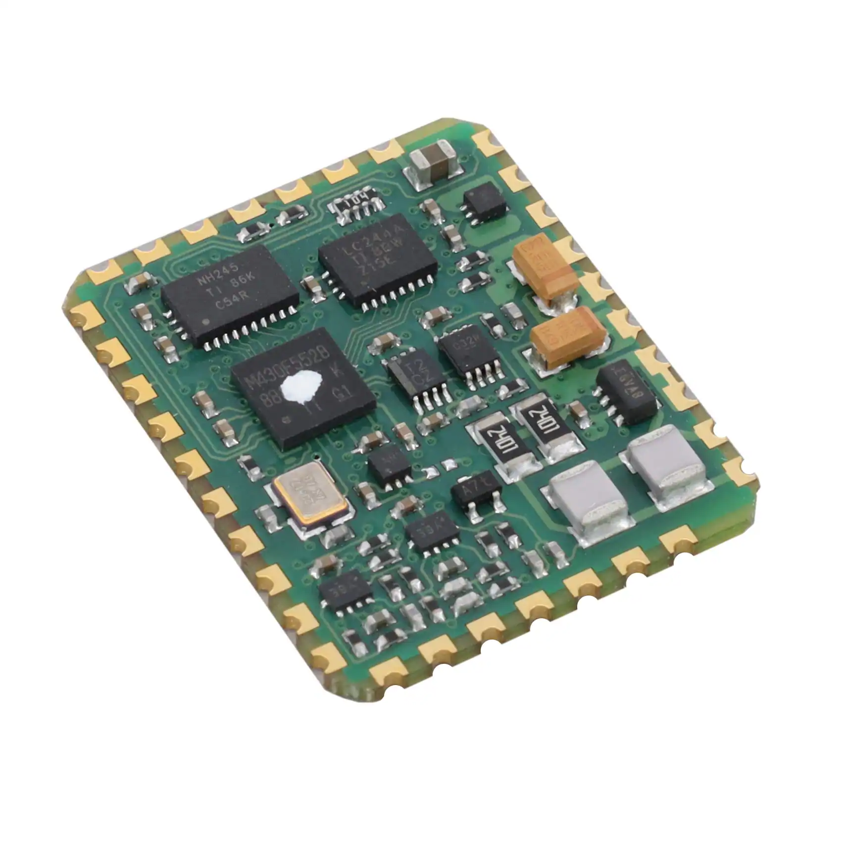


 工商网监
湘ICP备2023018690号
工商网监
湘ICP备2023018690号
