User’s Guide
September 2012
SD3GDAIII User’s Guide
9/20/2012
SD3GDA III User’s Guide
Lit#SNLU112
September 2012
�Contents
1
INTRODUCTION .......................................................................................................... 1
2
SETUP .......................................................................................................................... 2
2.1
Software Installation .............................................................................................................2
2.2
Connecting the Evaluation Board ..........................................................................................3
2.3
Jumper and Option Settings ...................................................................................................4
3
RUNNING THE GUI...................................................................................................... 5
3.1
Overview ................................................................................................................................5
3.2
Direct Read/Write to registers ................................................................................................5
3.3
Equalizer Control Page ..........................................................................................................6
3.4
Reclocker Control Page..........................................................................................................7
3.5
Eye Monitor Page...................................................................................................................8
4
MEDIA CARD ............................................................................................................... 8
5
BOARD SCHEMATICS ................................................................................................ 9
5.1
Equalizer Section ...................................................................................................................9
5.2
Reclocker Section.................................................................................................................10
5.3
Cable Driver .........................................................................................................................11
5.4
USB Interface .......................................................................................................................12
5.5
Power ...................................................................................................................................13
5.6
Media Board .........................................................................................................................14
6
BOARD LAYOUT ....................................................................................................... 15
6.1
Top Layer .............................................................................................................................15
6.2
GND-1 Layer .......................................................................................................................16
6.3
GND-2 Layer .......................................................................................................................17
6.4
Sig-1 Layer ...........................................................................................................................18
6.5
GND-3 Layer .......................................................................................................................19
6.6
Vcc Layer .............................................................................................................................20
6.7
GND-4 Layer .......................................................................................................................21
6.8
Bottom Layer .......................................................................................................................22
September 2012
7
BILL OF MATERIALS ................................................................................................ 23
8
EVALUATION BOARD/KIT/MODULE (EVM) ADDITIONAL TERMS ...................... 25
SD3GDAIII
User’s Guide
ii
�Figures
Figure 1 SD3GDAIII EVM Block Diagram ..................................................................................................................... 1
Figure 2 Equalizer Section Schematic .......................................................................................................................... 9
Figure 3 Reclocker Section Schematic ....................................................................................................................... 10
Figure 4 Cable Driver Section Schematic ................................................................................................................... 11
Figure 5 USB Interface Section Schematic ................................................................................................................ 12
Figure 6 Power Management Section Schematic....................................................................................................... 13
Figure 7 Media Board Schematic ............................................................................................................................... 14
iii
SD3GDA III User’s Guide
Lit#SNLU112
September 2012
��User’s Guide
September 2012
SD3GDAIII User’s Guide
1 Introduction
The SD3GDAIII is a kit containing an evaluation board which is functionally an SDI
Distribution Amplifier with a serial interface to allow connection to a host computer and a
graphical user interface (GUI) program which allows the configuration of the devices on the
board to be changed as desired, and allows for some measurements to be made on the board.
SD3GDA III User’s Guide
Lit#SNLU112
September 2012
�2 Setup
2.1 Software Installation
A copy of the install program can be obtained either from the CD encosed with the kit or
downloaded from http://www.ti.com/tool/sd3gdaiii. This installer will run and give you this
initial window:
Once the installer has initialized, it will prompt you for locations to store the files. The SD3GDAIII GUI
is built on the National Instruments LabView platform, so in addition to the GUI files, the installer will
install some National Instruments software.
September 2012
SD3GDAIII
User’s Guide
2
�2.2 Connecting the Evaluation Board
The SD3GDAIII requires an external power source – it will do it’s own power regulation, so any
power supply from 12V to 20VDC may be used, connect power via the spade terminals at the top of
the board. Once power is applied, connect the board to a USB port on the host computer with the
enclosed cable, and provide the input with an SDI source signal. The source can be any of the
270Mbps, 1.5Gbps or 3Gbps data rates.
Presence of an input signal is indicated with the ‘CD’ (carrier detect) LED close to J3 – the SDI input
port.
There are four BNC output connectors. Each output has the option for on board termination in the
event that the output is not being used. The bottom connector, J9 has R32 as it’s termination resistor,
and as shipped, R32 is NOT installed – this means that J9, SDO- may be used as the primary output.
The other three outputs (SDO+, SDO1- and SDO1-) have the termination resistor installed, so that the
cable driver will see properly terminated outputs. If you want to use these outputs, remove the
corresponding termination resistors (R23, R18 and R25).
3
SD3GDA III User’s Guide
Lit#SNLU112
September 2012
�2.3 Jumper and Option Settings
The SD3GDAIII has 5 locations for Jumper blocks, and several other option settings that are
enabled/disabled with 0Ω resistors.
Jumper
Function when installed
P1
Disables SDO1 (Output to Media Card) on LMH0395
P2
Disables SDO0 (Output to LMH0376) on LMH0395
JP1
Forces Cable driver into HD/3G mode
JP2
If in Pin Mode (via R15) then this makes the SDO1 on the LMH0376 the recovered
clock
JP5
If LMH0376 is in pin mode, a jumper here places the reclocker in Bypass
September 2012
SD3GDAIII
User’s Guide
4
�3 Running the GUI
3.1 Overview
Once setup, start the SD3GDAIII GUI, and it should open with a block diagram of the board:
From this page, you can select what to do next via the selection panel on the left of the screen.
3.2 Direct Read/Write to registers
The first option, ‘Low Level Configuration’ will allow you to examine individual register contents and write to
them. Clicking on this option will bring up this screen:
5
SD3GDA III User’s Guide
Lit#SNLU112
September 2012
�This screen shows each of the registers for each of the chips in the signal path on the board, and for each
register it will show what the last value read from that register was, what the last value written was, and by
clicking on one of the registers, it will give detail on each of the bits in the register. You can read individual
registers and you can write to the individual registers through this page. If you set up a particular configuration
for a part which you would like to reuse in the future, you can use the ‘Save Configuration’ and ‘Load
Configuration’ buttons to save and recover settings for a part.
3.3 Equalizer Control Page
Selecting the Equalizer page brings up a page which reports the status of the equalizer, Some of the settings,
such as the output settings can be set, but many of the other fields report status of the device.
September 2012
SD3GDAIII
User’s Guide
6
�3.4 Reclocker Control Page
The reclocker page allows you to control the LMH0376 – there are output setting to allow the two outputs to be
independently controlled for amplitude, offset and de-emphasis. If the LMH0376 is locked, this will be shown
with the green indicator on the bottom left of the page, and the nominal rate at which the device is locked is
shown. The user will also be able to read the Horizontal eye opening, and Vertical eye opening values from
the GUI.
7
SD3GDA III User’s Guide
Lit#SNLU112
September 2012
�3.5 Eye Monitor Page
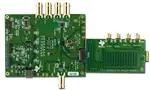
4 Media Card
The SD3GDAIII card has a media card inserted in the signal path between the equalizer and the reclocker.
This card may be inserted in order to insert 25cm, 50cm or 100cm of PCB trace between the equalizer and
the reclocker, to help the user to better simulate the use of the parts in a real system. Insert the media
card into the MEDIA BOARD CONNECTOR – the length of trace is shown on the media card next to the
fingers. There is also an option to use another card, connected with the SMA connectors on the Media
Card, if the card is inserted appropriately.
September 2012
SD3GDAIII
User’s Guide
8
�5 Board Schematics
5.1 Equalizer Section
Figure 2 Equalizer Section Schematic
9
SD3GDA III User’s Guide
Lit#SNLU112
September 2012
�5.2 Reclocker Section
Figure 3 Reclocker Section Schematic
September 2012
10
SD3GDAIII
User’s Guide
�5.3 Cable Driver
Figure 4 Cable Driver Section Schematic
11
SD3GDA III User’s Guide
Lit#SNLU112
September 2012
�5.4 USB Interface
Figure 5 USB Interface Section Schematic
September 2012
12
SD3GDAIII
User’s Guide
�5.5 Power
Figure 6 Power Management Section Schematic
13
SD3GDA III User’s Guide
Lit#SNLU112
September 2012
�5.6 Media Board
Figure 7 Media Board Schematic
September 2012
14
SD3GDAIII
User’s Guide
�6 Board Layout
6.1 Top Layer
15
SD3GDA III User’s Guide
Lit#SNLU112
September 2012
�6.2 GND-1 Layer
September 2012
16
SD3GDAIII
User’s Guide
�6.3 GND-2 Layer
17
SD3GDA III User’s Guide
Lit#SNLU112
September 2012
�6.4 Sig-1 Layer
September 2012
18
SD3GDAIII
User’s Guide
�6.5 GND-3 Layer
19
SD3GDA III User’s Guide
Lit#SNLU112
September 2012
�6.6 Vcc Layer
September 2012
20
SD3GDAIII
User’s Guide
�6.7 GND-4 Layer
21
SD3GDA III User’s Guide
Lit#SNLU112
September 2012
�6.8 Bottom Layer
September 2012
22
SD3GDAIII
User’s Guide
�7 Bill of Materials
Designator
Description
Comment
Quantity
C1, C4
C2, C3, C5, C6, C7, C8,
C9, C10, C11, C12, C13,
C14, C15, C16, C17, C18,
C19, C20, C21, C22, C23,
C24, C25
C27, C34, C35, C38, C39,
C52, C54
CAP, CERM, 47pF, 50V, +/-5%, C0G/NP0, 0603
06035A470JAT2A
Capacitor, 4.7uF, 6.3V, X5R, 0402
4.7uF
GRM188R71H104KA93
D
23
C29, C40, C53, C55
CAP, CERM, 4.7uF, 16V, +/-10%, X7R, 1206
4
C30, C31
CAP, CERM, 30pF, 100V, +/-5%, C0G/NP0, 0603
C32
CAP, CERM, 0.022uF, 16V, +/-10%, X7R, 0603
C3216X7R1C475K
GRM1885C2A300JA01
D
GRM188R71C223KA01
D
C36, C42, C43
CAP, CERM, 10uF, 50V, +/-20%, X7R, 2220
C5750X7R1H106M
3
C37, C44
CAP, CERM, 1uF, 50V, +/-10%, X7R, 1206
2
C41
C63, C64, C69, C70, C74,
C75, C76, C77, C90, C91
CAP, CERM, 100uF, 6.3V, +/-20%, X5R, 1206
CAP, CERM, 0.47uF, 16V, +/-10%, X7R, 0603
C3216X7R1H105K
GRM31CR60J107ME39
L
GRM188R71C474KA88
D
C65
CAP, CERM, 0.1uF, 16V, +/-5%, X7R, 0603
0603YC104JAT2A
1
C66
CAP, CERM, 220pF, 50V, +/-1%, C0G/NP0, 0603
06035A221FAT2A
1
Cff1, Css1
D1, D2, D3, D4, D5, D6,
D7, D8, D9, D10
CAP, CERM, 0.022uF, 100V, +/-5%, X7R, 0805
08051C223JAT2A
2
LED, Green, 0603
LED
F1, F2
J1, J2, J4, J5, MBJ1,
MBJ2, MBJ3, MBJ4
card edge connector 20-Pin, Dual row
Mate to HSEC8
2
SMA Edge Launch
SMA_R_EDGE
8
J3, J6, J7, J8, J9
BNC, Trompeter, 75-ohm, edge launch
BNC_EDGE
5
J10
JP1, JP2, JP3, JP4, JP5,
JP6
Connector, Recpt, USB-B, Mini, 5-pins, SMT
CONN_USB_1734328
1
Header, 2x1, 0.1"
HDR_2
6
JP16
PIN HEADER, 4x1, 0.1" PITCH
HDR_4
1
L1, L2, L3, L4, L5
5.6nH, 0402, Inductor
5.6nH
5
L7, L8
OPT1, OPT2, OPT4,
OPT5, OPT6, OPT9,
OPT10, OPT11, OPT12,
OPT13, OPT14, OPT15,
OPT16, OPT17, OPT18,
OPT19, OPT20, OPT21,
OPT22, OPT23, OPT24,
OPT26, OPT27, OPT28,
OPT29, OPT30, OPT31,
OPT32, OPT33, OPT34,
OPT35, OPT36, OPT37,
OPT38, OPT39, R12, R13,
R67
INDUCTOR 10UH 100MA 0805
10uH
2
RES, 0 ohm, 5%, 0.1W, 0603
CRCW06030000Z0EA
OPT3, OPT7, R2
OPT8, OPT25, R5, R8,
R10, R11, R14, R15, R17
RES, 0 ohm, 5%, 0.063W, 0402
ERJ-2GE0R00X
3
RES, 10k ohm, 5%, 0.1W, 0603
CRCW060310K0JNEA
9
P1, P2
Power Supply Terminal
SDO1 Disable
2
23
CAP, CERM, 0.1uF, 50V, +/-10%, X7R, 0603
SD3GDA III User’s Guide
Lit#SNLU112
2
7
2
1
1
10
10
38
September 2012
�P3
Header, 3-Pin
MHDR1X3
1
P4, P5
CONN HEADER 16POS .100 STR TIN
Header 8X2
2
P6
Header, 20-Pin, Dual row
HSEC8
1
PST1, PST2
R1, R3, R4, R6, R7, R9,
R16, R18, R19, R20, R21,
R22, R23, R24, R25, R26,
R27, R28, R29, R30, R31,
R32
Power Supply Terminal
SDO1 Disable
2
75 Ohm Resistor, 0402
75
R33, R34
RES, 33 ohm, 5%, 0.063W, 0402
CRCW040233R0JNED
2
R36, R52
RES, 1.00 ohm, 1%, 0.1W, 0603
RC0603FR-071RL
2
R37
RES, 1.5k ohm, 5%, 0.063W, 0402
CRCW04021K50JNED
1
R38
RES, 68.1k ohm, 1%, 0.1W, 0603
CRCW060368K1FKEA
1
R39
RES, 61.9k ohm, 1%, 0.1W, 0603
CRCW060361K9FKEA
1
R40
RES, 3.32k ohm, 1%, 0.1W, 0603
CRCW06033K32FKEA
1
R41
RES, 11.8k ohm, 1%, 0.1W, 0603
CRCW060311K8FKEA
1
R42
RES, 1.07k ohm, 1%, 0.1W, 0603
CRCW06031K07FKEA
1
R56, R61, R64, R70
RES, 10.0 ohm, 1%, 0.1W, 0603
CRCW060310R0FKEA
4
R57, R59
R58, R60, R62, R63, R65,
R66
RES, 1.00k ohm, 0.1%, 0.1W, 0603
RG1608P-102-B-T5
2
RES, 10.0k ohm, 0.1%, 0.1W, 0603
RG1608P-103-B-T5
6
R68
RES, 33k ohm, 5%, 0.063W, 0402
CRCW040233K0JNED
1
R69
RES, 1.2Meg ohm, 5%, 0.1W, 0603
CRCW06031M20JNEA
1
S1
DIP Switch, 2 Position, SPST
SW DIP-2
1
U1
SDI Equalizer
LMH0395
1
U2, U5
IC INVERTER
SN74AHC1G04
2
U3
IC BUFFER
SN74LVC1G125
1
U4
SDI Reclocker
LMH0376
1
U6
LMH0309 Cable Driver
LMH0309
1
U7
IC, 4-Chan ESD-Protection Array
TPD4E004DRY
1
U8
MSP430F5529
1
U14, U16, U19, U20, U22
Microcontroller
Ultra Low Noise, 150mA Linear Regulator for RF/Analog Circuits
Requires No Bypass Capacitor
LP5900SD-2.5
5
U17
Simple Switcher Power Module
LMZ14203TZ
1
U21
Quadruple 2-Input Positive-NAND Gate
SN74HC00D
1
X1
27 MHz VCXO
1
Y1
Crystal, SMT Quart Crystal
27MHz_CRYSTAL
CRYSTAL_ATSSM_SERIES
September 2012
24
SD3GDAIII
22
User’s Guide
1
�8 EVALUATION BOARD/KIT/MODULE (EVM) ADDITIONAL TERMS
Texas Instruments (TI) provides the enclosed Evaluation Board/Kit/Module (EVM) under the following conditions:
The user assumes all responsibility and liability for proper and safe handling of the goods. Further, the user
indemnifies TI from all claims arising from the handling or use of the goods.
Should this evaluation board/kit not meet the specifications indicated in the User’s Guide, the board/kit may be
returned within 30 days from the date of delivery for a full refund. THE FOREGOING LIMITED WARRANTY IS THE
EXCLUSIVE WARRANTY MADE BY SELLER TO BUYER AND IS IN LIEU OF ALL OTHER WARRANTIES,
EXPRESSED, IMPLIED, OR STATUTORY, INCLUDING ANY WARRANTY OF MERCHANTABILITY OR FITNESS
FOR ANY PARTICULAR PURPOSE. EXCEPT TO THE EXTENT OF THE INDEMNITY SET FORTH ABOVE,
NEITHER PARTY SHALL BE LIABLE TO THE OTHER FOR ANY INDIRECT, SPECIAL, INCIDENTAL, OR
CONSEQUENTIAL DAMAGES.
Please read the User's Guide and, specifically, the Warnings and Restrictions notice in the User's Guide prior to
handling the product. This notice contains important safety information about temperatures and voltages. For
additional information on TI's environmental and/or safety programs, please visit www.ti.com/esh or contact TI.
No license is granted under any patent right or other intellectual property right of TI covering or relating to any
machine, process, or combination in which such TI products or services might be or are used. TI currently deals
with a variety of customers for products, and therefore our arrangement with the user is not exclusive. TI assumes
no liability for applications assistance, customer product design, software performance, or infringement of patents
or services described herein.
REGULATORY COMPLIANCE INFORMATION
As noted in the EVM User’s Guide and/or EVM itself, this EVM and/or accompanying hardware may or may not be
subject to the Federal Communications Commission (FCC) and Industry Canada (IC) rules.
For EVMs not subject to the above rules, this evaluation board/kit/module is intended for use for ENGINEERING
DEVELOPMENT, DEMONSTRATION OR EVALUATION PURPOSES ONLY and is not considered by TI to be a
finished end product fit for general consumer use. It generates, uses, and can radiate radio frequency energy and
has not been tested for compliance with the limits of computing devices pursuant to part 15 of FCC or ICES-003
rules, which are designed to provide reasonable protection against radio frequency interference. Operation of the
equipment may cause interference with radio communications, in which case the user at his own expense will be
required to take whatever measures may be required to correct this interference.
General Statement for EVMs including a radio
User Power/Frequency Use Obligations: This radio is intended for development/professional use only in legally
allocated frequency and power limits. Any use of radio frequencies and/or power availability of this EVM and its
development application(s) must comply with local laws governing radio spectrum allocation and power limits for
this evaluation module. It is the user’s sole responsibility to only operate this radio in legally acceptable frequency
space and within legally mandated power limitations. Any exceptions to this are strictly prohibited and unauthorized
by Texas Instruments unless user has obtained appropriate experimental/development licenses from local
regulatory authorities, which is responsibility of user including its acceptable authorization.
For EVMs annotated as FCC – FEDERAL COMMUNICATIONS COMMISSION Part 15 Compliant
Caution
This device complies with part 15 of the FCC Rules. Operation is subject to the following two conditions: (1) This
device may not cause harmful interference, and (2) this device must accept any interference received, including
interference that may cause undesired operation.
Changes or modifications not expressly approved by the party responsible for compliance could void the user's
authority to operate the equipment.
25
SD3GDA III User’s Guide
Lit#SNLU112
September 2012
�FCC Interference Statement for Class A EVM devices
This equipment has been tested and found to comply with the limits for a Class A digital device, pursuant to part 15
of the FCC Rules. These limits are designed to provide reasonable protection against harmful interference when
the equipment is operated in a commercial environment. This equipment generates, uses, and can radiate radio
frequency energy and, if not installed and used in accordance with the instruction manual, may cause harmful
interference to radio communications. Operation of this equipment in a residential area is likely to cause harmful
interference in which case the user will be required to correct the interference at his own expense.
FCC Interference Statement for Class B EVM devices
This equipment has been tested and found to comply with the limits for a Class B digital device, pursuant to part 15
of the FCC Rules. These limits are designed to provide reasonable protection against harmful interference in a
residential installation. This equipment generates, uses and can radiate radio frequency energy and, if not installed
and used in accordance with the instructions, may cause harmful interference to radio communications. However,
there is no guarantee that interference will not occur in a particular installation. If this equipment does cause
harmful interference to radio or television reception, which can be determined by turning the equipment off and on,
the user is encouraged to try to correct the interference by one or more of the following measures:
•
•
•
•
Reorient or relocate the receiving antenna.
Increase the separation between the equipment and receiver.
Connect the equipment into an outlet on a circuit different from that to which the receiver is connected.
Consult the dealer or an experienced radio/TV technician for help.
For EVMs annotated as IC – INDUSTRY CANADA Compliant
This Class A or B digital apparatus complies with Canadian ICES-003.
Changes or modifications not expressly approved by the party responsible for compliance could void the user’s
authority to operate the equipment.
Concerning EVMs including radio transmitters
This device complies with Industry Canada licence-exempt RSS standard(s). Operation is subject to the following
two conditions: (1) this device may not cause interference, and (2) this device must accept any interference,
including interference that may cause undesired operation of the device.
Concerning EVMs including detachable antennas
Under Industry Canada regulations, this radio transmitter may only operate using an antenna of a type and
maximum (or lesser) gain approved for the transmitter by Industry Canada. To reduce potential radio interference to
other users, the antenna type and its gain should be so chosen that the equivalent isotropically radiated power
(e.i.r.p.) is not more than that necessary for successful communication.
This radio transmitter has been approved by Industry Canada to operate with the antenna types listed in the user
guide with the maximum permissible gain and required antenna impedance for each antenna type indicated.
Antenna types not included in this list, having a gain greater than the maximum gain indicated for that type, are
strictly prohibited for use with this device.
Cet appareil numérique de la classe A ou B est conforme à la norme NMB-003 du Canada.
Les changements ou les modifications pas expressément approuvés par la partie responsable de la conformité ont
pu vider l’autorité de l'utilisateur pour actionner l'équipement.
Concernant les EVMs avec appareils radio
Le présent appareil est conforme aux CNR d'Industrie Canada applicables aux appareils radio exempts de licence.
L'exploitation est autorisée aux deux conditions suivantes : (1) l'appareil ne doit pas produire de brouillage, et (2)
l'utilisateur de l'appareil doit accepter tout brouillage radioélectrique subi, même si le brouillage est susceptible d'en
compromettre le fonctionnement.
September 2012
26
SD3GDAIII
User’s Guide
�Concernant les EVMs avec antennes détachables
Conformément à la réglementation d'Industrie Canada, le présent émetteur radio peut fonctionner avec une
antenne d'un type et d'un gain maximal (ou inférieur) approuvé pour l'émetteur par Industrie Canada. Dans le but
de réduire les risques de brouillage radioélectrique à l'intention des autres utilisateurs, il faut choisir le type
d'antenne et son gain de sorte que la puissance isotrope rayonnée équivalente (p.i.r.e.) ne dépasse pas l'intensité
nécessaire à l'établissement d'une communication satisfaisante.
Le présent émetteur radio a été approuvé par Industrie Canada pour fonctionner avec les types d'antenne
énumérés dans le manuel d’usage et ayant un gain admissible maximal et l'impédance requise pour chaque type
d'antenne. Les types d'antenne non inclus dans cette liste, ou dont le gain est supérieur au gain maximal indiqué,
sont strictement interdits pour l'exploitation de l'émetteur.
SPACER
SPACER
SPACER
【Important Notice for Users of this Product in Japan】
This development kit is NOT certified as Confirming to Technical Regulations of Radio Law of Japan
If you use this product in Japan, you are required by Radio Law of Japan to follow the instructions below with
respect to this product:
1. Use this product in a shielded room or any other test facility as defined in the notification #173 issued by
Ministry of Internal Affairs and Communications on March 28, 2006, based on Sub-section 1.1 of Article 6
of the Ministry’s Rule for Enforcement of Radio Law of Japan,
2. Use this product only after you obtained the license of Test Radio Station as provided in Radio Law of
Japan with respect to this product, or
3. Use of this product only after you obtained the Technical Regulations Conformity Certification as provided
in Radio Law of Japan with respect to this product. Also, please do not transfer this product, unless you
give the same notice above to the transferee. Please note that if you could not follow the instructions
above, you will be subject to penalties of Radio Law of Japan.
Texas Instruments Japan Limited
(address) 24-1, Nishi-Shinjuku 6 chome, Shinjuku-ku, Tokyo, Japan
http://www.tij.co.jp
【ご使用にあたっての注】
本開発キットは技術基準適合証明を受けておりません。
本製品のご使用に際しては、電波法遵守のため、以下のいずれかの措置を取っていただく必要がありますのでご注
意ください。
1. 電波法施行規則第6条第1項第1号に基づく平成18年3月28日総務省告示第173号で定められた電波暗室等の
試験設備でご使用いただく。
2. 実験局の免許を取得後ご使用いただく。
3. 技術基準適合証明を取得後ご使用いただく。
なお、本製品は、上記の「ご使用にあたっての注意」を譲渡先、移転先に通知しない限り、譲渡、移転できないも
のとします。
上記を遵守頂けない場合は、電波法の罰則が適用される可能性があることをご留意ください。
日本テキサス・インスツルメンツ株式会社
東京都新宿区西新宿6丁目24番1号
西新宿三井ビル
http://www.tij.co.jp
SPACER
SPACER
27
SD3GDA III User’s Guide
Lit#SNLU112
September 2012
�EVALUATION BOARD/KIT/MODULE (EVM)
WARNINGS, RESTRICTIONS AND DISCLAIMERS
For Feasibility Evaluation Only, in Laboratory/Development Environments. Unless otherwise indicated, this
EVM is not a finished electrical equipment and not intended for consumer use. It is intended solely for use for
preliminary feasibility evaluation in laboratory/development environments by technically qualified electronics experts
who are familiar with the dangers and application risks associated with handling electrical mechanical components,
systems and subsystems. It should not be used as all or part of a finished end product.
Your Sole Responsibility and Risk. You acknowledge, represent and agree that:
1. You have unique knowledge concerning Federal, State and local regulatory requirements (including but not
limited to Food and Drug Administration regulations, if applicable) which relate to your products and which
relate to your use (and/or that of your employees, affiliates, contractors or designees) of the EVM for
evaluation, testing and other purposes.
2. You have full and exclusive responsibility to assure the safety and compliance of your products with all
such laws and other applicable regulatory requirements, and also to assure the safety of any activities to be
conducted by you and/or your employees, affiliates, contractors or designees, using the EVM. Further, you
are responsible to assure that any interfaces (electronic and/or mechanical) between the EVM and any
human body are designed with suitable isolation and means to safely limit accessible leakage currents to
minimize the risk of electrical shock hazard.
3. You will employ reasonable safeguards to ensure that your use of the EVM will not result in any property
damage, injury or death, even if the EVM should fail to perform as described or expected.
4. You will take care of proper disposal and recycling of the EVM’s electronic components and packing
materials.
Certain Instructions. It is important to operate this EVM within TI’s recommended specifications and
environmental considerations per the user guidelines. Exceeding the specified EVM ratings (including but not
limited to input and output voltage, current, power, and environmental ranges) may cause property damage,
personal injury or death. If there are questions concerning these ratings please contact a TI field representative
prior to connecting interface electronics including input power and intended loads. Any loads applied outside of the
specified output range may result in unintended and/or inaccurate operation and/or possible permanent damage to
the EVM and/or interface electronics. Please consult the EVM User's Guide prior to connecting any load to the EVM
output. If there is uncertainty as to the load specification, please contact a TI field representative. During normal
operation, some circuit components may have case temperatures greater than 60°C as long as the input and output
are maintained at a normal ambient operating temperature. These components include but are not limited to linear
regulators, switching transistors, pass transistors, and current sense resistors which can be identified using the
EVM schematic located in the EVM User's Guide. When placing measurement probes near these devices during
normal operation, please be aware that these devices may be very warm to the touch. As with all electronic
evaluation tools, only qualified personnel knowledgeable in electronic measurement and diagnostics normally found
in development environments should use these EVMs.
Agreement to Defend, Indemnify and Hold Harmless. You agree to defend, indemnify and hold TI, its licensors
and their representatives harmless from and against any and all claims, damages, losses, expenses, costs and
liabilities (collectively, "Claims") arising out of or in connection with any use of the EVM that is not in accordance
with the terms of the agreement. This obligation shall apply whether Claims arise under law of tort or contract or
any other legal theory, and even if the EVM fails to perform as described or expected.
Safety-Critical or Life-Critical Applications. If you intend to evaluate the components for possible use in safety
critical applications (such as life support) where a failure of the TI product would reasonably be expected to cause
September 2012
28
SD3GDAIII
User’s Guide
�severe personal injury or death, such as devices which are classified as FDA Class III or similar classification, then
you must specifically notify TI of such intent and enter into a separate Assurance and Indemnity Agreement.
Mailing Address: Texas Instruments, Post Office Box 655303, Dallas, Texas 75265
Copyright © 2012, Texas Instruments Incorporated
29
SD3GDA III User’s Guide
Lit#SNLU112
September 2012
�IMPORTANT NOTICE
Texas Instruments Incorporated and its subsidiaries (TI) reserve the right to make corrections, enhancements, improvements and other
changes to its semiconductor products and services per JESD46, latest issue, and to discontinue any product or service per JESD48, latest
issue. Buyers should obtain the latest relevant information before placing orders and should verify that such information is current and
complete. All semiconductor products (also referred to herein as “components”) are sold subject to TI’s terms and conditions of sale
supplied at the time of order acknowledgment.
TI warrants performance of its components to the specifications applicable at the time of sale, in accordance with the warranty in TI’s terms
and conditions of sale of semiconductor products. Testing and other quality control techniques are used to the extent TI deems necessary
to support this warranty. Except where mandated by applicable law, testing of all parameters of each component is not necessarily
performed.
TI assumes no liability for applications assistance or the design of Buyers’ products. Buyers are responsible for their products and
applications using TI components. To minimize the risks associated with Buyers’ products and applications, Buyers should provide
adequate design and operating safeguards.
TI does not warrant or represent that any license, either express or implied, is granted under any patent right, copyright, mask work right, or
other intellectual property right relating to any combination, machine, or process in which TI components or services are used. Information
published by TI regarding third-party products or services does not constitute a license to use such products or services or a warranty or
endorsement thereof. Use of such information may require a license from a third party under the patents or other intellectual property of the
third party, or a license from TI under the patents or other intellectual property of TI.
Reproduction of significant portions of TI information in TI data books or data sheets is permissible only if reproduction is without alteration
and is accompanied by all associated warranties, conditions, limitations, and notices. TI is not responsible or liable for such altered
documentation. Information of third parties may be subject to additional restrictions.
Resale of TI components or services with statements different from or beyond the parameters stated by TI for that component or service
voids all express and any implied warranties for the associated TI component or service and is an unfair and deceptive business practice.
TI is not responsible or liable for any such statements.
Buyer acknowledges and agrees that it is solely responsible for compliance with all legal, regulatory and safety-related requirements
concerning its products, and any use of TI components in its applications, notwithstanding any applications-related information or support
that may be provided by TI. Buyer represents and agrees that it has all the necessary expertise to create and implement safeguards which
anticipate dangerous consequences of failures, monitor failures and their consequences, lessen the likelihood of failures that might cause
harm and take appropriate remedial actions. Buyer will fully indemnify TI and its representatives against any damages arising out of the use
of any TI components in safety-critical applications.
In some cases, TI components may be promoted specifically to facilitate safety-related applications. With such components, TI’s goal is to
help enable customers to design and create their own end-product solutions that meet applicable functional safety standards and
requirements. Nonetheless, such components are subject to these terms.
No TI components are authorized for use in FDA Class III (or similar life-critical medical equipment) unless authorized officers of the parties
have executed a special agreement specifically governing such use.
Only those TI components which TI has specifically designated as military grade or “enhanced plastic” are designed and intended for use in
military/aerospace applications or environments. Buyer acknowledges and agrees that any military or aerospace use of TI components
which have not been so designated is solely at the Buyer's risk, and that Buyer is solely responsible for compliance with all legal and
regulatory requirements in connection with such use.
TI has specifically designated certain components which meet ISO/TS16949 requirements, mainly for automotive use. Components which
have not been so designated are neither designed nor intended for automotive use; and TI will not be responsible for any failure of such
components to meet such requirements.
Products
Applications
Audio
www.ti.com/audio
Automotive and Transportation
www.ti.com/automotive
Amplifiers
amplifier.ti.com
Communications and Telecom
www.ti.com/communications
Data Converters
dataconverter.ti.com
Computers and Peripherals
www.ti.com/computers
DLP® Products
www.dlp.com
Consumer Electronics
www.ti.com/consumer-apps
DSP
dsp.ti.com
Energy and Lighting
www.ti.com/energy
Clocks and Timers
www.ti.com/clocks
Industrial
www.ti.com/industrial
Interface
interface.ti.com
Medical
www.ti.com/medical
Logic
logic.ti.com
Security
www.ti.com/security
Power Mgmt
power.ti.com
Space, Avionics and Defense
www.ti.com/space-avionics-defense
Microcontrollers
microcontroller.ti.com
Video and Imaging
www.ti.com/video
RFID
www.ti-rfid.com
OMAP Applications Processors
www.ti.com/omap
TI E2E Community
e2e.ti.com
Wireless Connectivity
www.ti.com/wirelessconnectivity
Mailing Address: Texas Instruments, Post Office Box 655303, Dallas, Texas 75265
Copyright © 2012, Texas Instruments Incorporated
�


 工商网监
湘ICP备2023018690号
工商网监
湘ICP备2023018690号
