�����
���� ����
�������
������� ��
��
����
�����
User’s Guide
July 2000
AAP Data Transmission
SLLU013
�Trademarks
Preface
Read This First
About This Manual
This is the user’s guide for the SN65LVDS387EVM and SN65LVDS386 evaluation modules (EVMs). It contains information on the evaluation modules
(EVMs) for Texas Instruments’ SN65LVDS387 16-channel LVDS driver and for
the SN65LVDS386 16-channel LVDS receiver.
Two separate EVMs are available, allowing each LVDS device to be tested
individually using a single EVM for that device. If both EVMs are used, the
LVDS output signals from the SN65LVDS387EVM 16-channel LVDS driver
can be connected to the LVDS inputs of the 16-channel LVDS receiver on the
SN65LVDS386EVM. This allows users to simulate performance of an LVDS
system. Recommended test equipment and evaluation and interconnect
guidelines are provided for both 16-channel point-to-point and multidrop
configurations. The EVMs are CE compliant for distribution within the
European Community.
How to Use This Manual
This document contains the following chapters:
� Chapter 1 – Introduction
� Chapter 2 – The Evaluation Boards
� Chapter 3 – Equipment Required
� Chapter 4 – Operation
� Appendix A – Parts List and Schematics
Trademarks
BergStick is a registered trademark of Berg Electronics. All other trademarks
are the property of their respective owners.
Read This First
iii
�Running Title—Attribute Reference
Contents
1
Introduction . . . . . . . . . . . . . . . . . . . . . . . . . . . . . . . . . . . . . . . . . . . . . . . . . . . . . . . . . . . . . . . . . . . . . 1-1
2
The Evaluation Boards . . . . . . . . . . . . . . . . . . . . . . . . . . . . . . . . . . . . . . . . . . . . . . . . . . . . . . . . . . . 2-1
2.1
SN65LVDS387 16-Channel LVDS Line Driver . . . . . . . . . . . . . . . . . . . . . . . . . . . . . . . . . . 2-3
2.2
SN65LVDS386 16-Channel LVDS Line Receiver . . . . . . . . . . . . . . . . . . . . . . . . . . . . . . . . 2-5
3
Equipment Required . . . . . . . . . . . . . . . . . . . . . . . . . . . . . . . . . . . . . . . . . . . . . . . . . . . . . . . . . . . . .
3.1
Pattern Generator . . . . . . . . . . . . . . . . . . . . . . . . . . . . . . . . . . . . . . . . . . . . . . . . . . . . . . . . . .
3.2
Oscilloscope and Scope Probes . . . . . . . . . . . . . . . . . . . . . . . . . . . . . . . . . . . . . . . . . . . . . .
3.3
Power Supply . . . . . . . . . . . . . . . . . . . . . . . . . . . . . . . . . . . . . . . . . . . . . . . . . . . . . . . . . . . . . .
3.4
Cables . . . . . . . . . . . . . . . . . . . . . . . . . . . . . . . . . . . . . . . . . . . . . . . . . . . . . . . . . . . . . . . . . . . .
3-1
3-2
3-2
3-2
3-2
4
Operation . . . . . . . . . . . . . . . . . . . . . . . . . . . . . . . . . . . . . . . . . . . . . . . . . . . . . . . . . . . . . . . . . . . . . . .
4.1
SN65LVDS387 Operation . . . . . . . . . . . . . . . . . . . . . . . . . . . . . . . . . . . . . . . . . . . . . . . . . . . .
4.2
SN65LVDS386 Operation . . . . . . . . . . . . . . . . . . . . . . . . . . . . . . . . . . . . . . . . . . . . . . . . . . . .
4.3
System Evaluation Using Both the SN65LVDS387EVM and SN65LVDS386EVM . . . .
4.3.1 Point-to-Point Configuration . . . . . . . . . . . . . . . . . . . . . . . . . . . . . . . . . . . . . . . . . . .
4.3.2 Multidrop Configuration . . . . . . . . . . . . . . . . . . . . . . . . . . . . . . . . . . . . . . . . . . . . . . .
4.4
References . . . . . . . . . . . . . . . . . . . . . . . . . . . . . . . . . . . . . . . . . . . . . . . . . . . . . . . . . . . . . . . .
4-1
4-2
4-3
4-3
4-3
4-3
4-5
A
Parts List and Schematics . . . . . . . . . . . . . . . . . . . . . . . . . . . . . . . . . . . . . . . . . . . . . . . . . . . . . . . A-1
A.1 Parts List for EVMs . . . . . . . . . . . . . . . . . . . . . . . . . . . . . . . . . . . . . . . . . . . . . . . . . . . . . . . . . A-2
A.2 Schematic Diagrams 6420201 and 6420202 . . . . . . . . . . . . . . . . . . . . . . . . . . . . . . . . . . . A-3
Chapter Title—Attribute Reference
v
�Running Title—Attribute Reference
Figures
2–1.
2–2.
2–3.
4–1.
vi
EVM Simplified I/O Block Diagram . . . . . . . . . . . . . . . . . . . . . . . . . . . . . . . . . . . . . . . . . . . . . .
SN65LVDS387EVM . . . . . . . . . . . . . . . . . . . . . . . . . . . . . . . . . . . . . . . . . . . . . . . . . . . . . . . . . . .
SN65LVDS386EVM . . . . . . . . . . . . . . . . . . . . . . . . . . . . . . . . . . . . . . . . . . . . . . . . . . . . . . . . . . .
Examples of Multidrop Interconnections . . . . . . . . . . . . . . . . . . . . . . . . . . . . . . . . . . . . . . . . . .
2-2
2-4
2-6
4-4
�Chapter 1
Introduction
This is the user’s guide for the evaluation modules (EVMs) for the Texas Instruments’ SN65LVDS387EVM 16-channel LVDS driver EVM and the
SN65LVDS386EVM 16-channel LVDS receiver EVM. One manual is used for
both EVMs because the boards are similar for both devices. The EVMs are
CE-compliant for distribution within the European Community.
Low-voltage differential signaling (LVDS), as documented in TIA/EIA-644, is
a balanced signaling method used for high-speed transmission of binary data
over copper. It is well recognized that the benefits of balanced-data transmission begin to outweigh the cost advantages of single-ended techniques when
signal-transition times approach 10 nS. This represents signaling rates approaching 30 Megabits per second (Mbps) Presently, LVDS devices operate
with signaling rates in the hundreds of Mbps. This performance is achieved
with reduced power consumption and reduced electromagnetic interference
(EMI) emissions compared to other data transmission standards, such as
TIA/EIA–422 and TIA/EIA–232 (also known as RS–232 and RS–422, respectively), PECL, etc. Project collateral discussed in this user’s guide can be
downloaded from the following URL: http://www.ti.com/lit/zip/SLLU013.
Note:
To Designers
Both EVMs use the same printed-wiring board (PWB). The 387 device is
mounted with the device’s pin 1 facing the top of the PWB, and the 386 is
mounted with the device’s pin 1 facing the bottom of the PWB.
Introduction
1-1
�Chapter 2
The Evaluation Boards
Each EVM consists of a six-layer printed-wiring board (PWB). The LVDS
device and BergStick connectors are on the top (connector side) of the
board. All other passive components are installed on the underside
(component side) of the PWB. A simplified input/output (I/O) block diagram of
the EVM is shown in Figure 2–1.
Topic
Page
2.1
SN65LVDS387 16-Channel LVDS Line Driver . . . . . . . . . . . . . . . . . . . . 2-3
2.2
SN65LVDS386 16-Channel LVDS Line Receiver . . . . . . . . . . . . . . . . . . 2-5
The Evaluation Boards
2-1
�Figure 2–1. EVM Simplified I/O Block Diagram
LVTTL Input
Connector
VCC GND
LVDS Output
Connector
LVTTL Output
VCC GND
Connector
LVDS Input
Connector
EN_A
EN_A
A1Y
A1Z
A1A
51
D4Y
100
D4B
D4A
A2Y
A2Z
A2A
D3B
D3Y
D3A
A3Y
A3Z
A3A
D2B
D2Y
D2A
A4Y
A4Z
A4A
LVDS Driver
(1 of 4)
LVDS387EVM
D1B
D1Y
LVDS Receiver
(1 of 4)
D1A
LVDS386EVM
The SN65LVDS387EVM and the SN65LVDS386EVM are discussed in sections 2.1 and 2.2. Use of the schematics in Appendix A will facilitate understanding the detailed discussion that follows.
2-2
�SN65LVDS387 16-Channel LVDS Line Driver
2.1 SN65LVDS387 16-Channel LVDS Line Driver
This 16-channel LVDS driver accepts 16 low-voltage TTL (LVTTL) inputs and
generates 16 LVDS differential outputs (please refer to the schematic in
Appendix I). Connectors P1/P2 are the LVTTL I/O connectors. Connectors P3
through P7 are the LVDS I/O connectors. The LVTTL inputs can be provided
by any suitable source. As shipped, the SN65LVDS387EVM has 50-Ω
termination resistors (R33 through R48) installed on each LVTTL input line to
accommodate inputs from a pattern generator or other instrumentation that
has a 50-Ω source impedance. If the LVTTL source and cable being used is
not a 50-Ω source, then these resistors (resistors R33 through R48) need to
be removed. They are required to match the characteristic impedance of the
cable (and the source impedance of most pattern generators). These resistors
are located on the back (under) side of the SN65LVDS386EVM, next to the
P1/P2 connector row.
The other optional components are resistors R1 through R32. Resistors R1
through R16 are left open on the SN65LVDS387EVM. These are used in the
LVDS output circuit and, since LVDS lines are normally terminated at the input
to the receiver, these 100-Ω resistors are not installed on the EVM. If users
want to measure specific performance parameters on the ’387, then they are
responsible for installing 100-ohm resistors in R1 through R16. Zero-ohm
resistors are installed in R17 through R32, which are in series with the LVTTL
inputs to the SN65LVDS387. The remaining components are connectors for
Vcc and Gnd connections, and decoupling capacitors for the LVDS device.
These components are the same for both configurations of the EVM.
There are also four jumpers (JMP1 through JMP4 ) located next to the P1/P2
connector row. These jumpers control the enable and disable for each fourchannel (quad) section of the device. Each of these jumpers consist of three
pins and a jumper short. The center pin is connected to the device and the outer pins (top and bottom) are VCC and GND. The jumper short can be moved
so contact is made between VCC and the enable/disable pin, or between GND
and the enable/disable pin. As shipped, the four jumper shorts are installed to
VCC so that all four sections of the device are enabled. A photograph of the
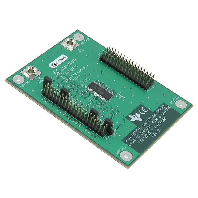
SN65LVDS387EVM is shown is Figure 2–2.
The Evaluation Boards
2-3
�SN65LVDS387 16-Channel LVDS Line Driver
Figure 2–2. SN65LVDS387EVM
LVTTL
Input Pins
GND
Enable/Disable
Jumpers
Connector (Top) Side
2-4
LVDS
VCC Output Pins
Component (Bottom) Side
�SN65LVDS386 16-Channel LVDS Line Receiver
2.2 SN65LVDS386 16-Channel LVDS Line Receiver
The SN65LVDS386EVM accepts 16 LVDS inputs and generates 16 LVTTL
outputs (refer to the schematic in Appendix I). Connectors P3 through P7
(right-side edge) accept the differential LVDS inputs and connector P1/P2 provides the LVTTL output signals. The as shipped configuration of the
SN65LVDS386 EVM also contains external resistors required for basic operation and testing of the device. Resistors R1 through R16 are 100-Ω resistors
which terminate each LVDS input channel. These are installed on the underside of the SN65LVDS386EVM, very close to the input pins of the device.
The LVTTL output-channels path (etch on the PWB) contains two pads where
external resistors may be installed. Resistors R17 through R32 are series resistors where zero-ohm resistors are normally installed. These are followed by
resistors R33 through R48, which allow a pull-down resistor to be installed after the series resistor (R17 through R32). As shipped, these pull-down resistors are not installed. The combination of these series (R17 through R32) and
pull-down resistors (R 33 through R48) allow the user to install a divider network if desired. This might be necessary if the outputs are to be measured with
an instrument having a 50-Ω input impedance. By installing a 475-Ω series resistor and a 50-Ω pull down resistor, a 20:1 divider is created (the 50-Ω pulldown in parallel with the 50-Ω input impedance equals 25 Ω, plus the 475-Ω
series impedance of the instrument, for a total load of 500 Ω on the output of
the receiver). As shipped, there is no resistor divider installed, and each device
LVTTL output is routed directly to the P1/P2 connectors through a 0-Ω resistor
(R17 through R32).
The remaining components are connectors for VCC and GND connections,
and decoupling capacitors for the LVDS device (these components are the
same for both EVM configurations).
There are also four jumpers (JMP1 through JMP4 ) located next to the P1/P2
connector row. These jumpers control the enable/disable for each four-channel (quad) section of the device. Each of these jumpers consist of three pins
and a jumper short. The center pin is connected to the device and the outer
pins (top and bottom) are VCC and GND. The jumper short can be moved so
contact is made between VCC and the enable/disable pin, or between GND
and the enable/disable pin. As shipped, the jumper shorts are installed to VCC
so that all four sections of the device are enabled.
The Evaluation Boards
2-5
�SN65LVDS386 16-Channel LVDS Line Receiver
Figure 2–3. SN65LVDS386EVM
LVTTL
Output Pins
GND
Enable/Disable
Jumpers
Connector (Top) Side
2-6
VCC
LVDS
Input Pins
Component (Bottom) Side
�Chapter 3
Equipment Required
This chapter provides guidance for selecting the test equipment required to
use the EVM.
Topic
Page
3.1
Pattern Generator . . . . . . . . . . . . . . . . . . . . . . . . . . . . . . . . . . . . . . . . . . . . . 3-2
3.2
Oscilloscope and Scope Probes . . . . . . . . . . . . . . . . . . . . . . . . . . . . . . . . 3-2
3.3
Power Supply . . . . . . . . . . . . . . . . . . . . . . . . . . . . . . . . . . . . . . . . . . . . . . . . . 3-2
3.4
Cables . . . . . . . . . . . . . . . . . . . . . . . . . . . . . . . . . . . . . . . . . . . . . . . . . . . . . . . 3-2
Equipment Required
3-1
�Pattern Generator
3.1 Pattern Generator
The SN65LVDS387 EVM requires a signal or pattern generator that can provide at least one LVTTL input signal to the device. The LVTTL signal levels provided to the SN65LVDS387EVM must have a VIH = 2 Vdc minimum. Sixteen
simultaneous LVTTL inputs are required to fully exercise the device, so a pattern generator with 16 parallel LVTTL outputs and a signaling-rate range up
to several hundred megabits-per-second (Mbps) is suggested. The Tektronix
HFS-series of pattern generators, or equivalent, can be used to provide the
LVTTL inputs signals. HFS-9DG1 plug-in cards are recommended as they can
be used to provide both single-ended inputs for the SN65LVDS387 driver and
differential inputs for the SN65LVDS386 receiver.
3.2 Oscilloscope and Scope Probes
The signaling rates and LVDS signal transitions are very fast (less than 1 nS).
To adequately monitor these signals will require an oscilloscope with a minimum bandwidth of 1 GHz. The probes need to have a similar bandwidth to prevent significant measurement errors. A Tektronix 784C oscilloscope with
P6243 or P6245 single-ended probes, and P6247 differential probes, or equivalent, is suggested.
3.3 Power Supply
A single-output dc power supply is required to provide Vcc and Gnd to the
EVM. This supply is connected to J1 (Vcc) and J2 (GND) on the EVM. An adjustable dc range of 2–4 Vdc and a current of 200 mA dc is required. When
testing both the SN65LVDS387EVM and SN65LVDS386EVM together as a
system, either a single 500-mA dc-supply can be used, or two separate power
supplies may be used so performance with different Vcc levels on each EVM
may be evaluated.
3.4 Cables
There are no cables provided with either the SN65LVDS387EVM or the
SN65LVDS386EVM. When evaluating either the SN65LVDS387EVM or
SN65LVDS386EVM separately, the only cables required are those connecting
the input signal source to the input of the EVM. When connecting the
SN65LVDS387EVM to the SN65LVDS386EVM to perform system tests, users
may evaluate system performance using different types and lengths of
cabling. This is done by inserting the bare conductor into the LVDS connectors
between the two EVMs (the conductors have to be exposed by removing
approximately 1 to 1.5 centimeters of insulation from each conductor). It is
recommended to select a cable with a characteristic impedance (Zo) of
100 Ω (±10%). Any cable which meets the requirements of EIA-568A Category
5 (CAT5) is recommended.
3-2
�Chapter 4
Operation
The SN65LVDS386 and SN65LVDS387 EVMs provide easy I/O connections
for instrumentation. This makes device testing quick and easy. Individual
channels can be tested and parameters evaluated for specific applications. In
addition, the EVMs are small and compact to allow the entire PWB to be placed
in a small temperature chamber. Also, the I/O connectors and enable jumpers
are located away from the device, and all external resistors are located on the
opposite side of the EVM. This also allows the use of a forced-air temperature
controller (such as a Thermostream, or a Temptronics system). The user will
notice that the boards are designed such that the LVTTL I/O connections are
made on the left side of the EVM (P1 and P2) and the LVDS I/O connections
are made on the right side of each EVM (P3).
Topic
Page
4.1
LVDS387 Operation . . . . . . . . . . . . . . . . . . . . . . . . . . . . . . . . . . . . . . . . . . . 4-2
4.2
LVDS386 Operation . . . . . . . . . . . . . . . . . . . . . . . . . . . . . . . . . . . . . . . . . . . 4-3
4.3
System Evaluation Using Both the SN65LVDS387EVM and
SN65LVDS386EVM . . . . . . . . . . . . . . . . . . . . . . . . . . . . . . . . . . . . . . . . . . . . 4-3
4.4
References . . . . . . . . . . . . . . . . . . . . . . . . . . . . . . . . . . . . . . . . . . . . . . . . . . . 4-5
Operation
4-1
�SN65LVDS387EVM Operation
4.1 SN65LVDS387EVM Operation
The SN65LVDS387EVM is ready to be used as shipped. When connected to
the test instrumentation and 3.3-Vdc power (as described in section 3),
performance can be tested and observed. All I/O connections are made using
standard BergSticks that allow fast and easy connections. These also allow
direct connections to oscilloscope probes. BergSticks are also used for the
enable/disable jumper posts to provide easy connection to external equipment
if device response to enable/disable is required. The jumper shorts can be
manually placed in either the VCC position (enabled) or the GND position
(disabled), or the jumper post can be removed to allow connection to external
equipment. Note that there is no 50-Ω termination onboard for the
enable/disable pins.
Basic tests of the SN65LVDS387 driver will consist of applying an LVTTL signal pattern to the P1/P2 input connector and monitoring the output of the driver.
When tested as a stand-alone device, 100-Ω termination resistors can be added to the scope probe, or individual 100-Ω termination resistors can be
installed on the board (backside of the SN65LVDS387EVM) at R1 through
R16. The scope termination is recommended for high-signaling rates to eliminate the stub effects caused by the PWB traces running to the P3 connector.
The input pins on connectors P1 and P2 stagger the input and ground pins row
to row. This is done to minimize channel-to-channel crosstalk and interference
between input channels. If an LVDS channel is not responding, check to make
sure the input connection has not been inverted.
4-2
�SN65LVDS386EVM Operation
4.2 SN65LVDS386EVM Operation
Like the SN65LVDS387EVM, the SN65LVDS386EVM is shipped with all required components already installed on the board, and is ready for testing. For
the LVDS386, differential inputs need to be provided to simulate the differential
output-voltage levels (Vod is nominally 400 mV) and common-mode outputvoltage inputs (nominally 1.2 Vdc) of an LVDS driver. These inputs are easily
connected to the right edge P3-P7 LVDS side of the SN65LVDS386EVM. The
LVTTL output signals can be monitored using a scope probe connected directly to the P1/P2 connector pin.
As shipped, each LVDS input channel is terminated with 100-Ω resistors (R1
through R16) across the receiver inputs. These resistors are located on the
backside of the EVM near the input pins of the device. Each LVTTL output pin
is routed directly to the P1/P2 connector row. There are provisions on the
SN65LVDS386EVM to install a series resistor and a pulldown resistor. This allows users to install a resistor divider on the output if required for testing the
device. But, as shipped, the series resistors (R17 through R32) have zero-ohm
resistors installed, and the pulldown resistors (R33 through R48) have no components installed.
4.3 System Evaluation Using Both the SN65LVDS387EVM and
SN65LVDS386EVM
These EVMs has been designed to allow performance evaluation of both devices when connected together. This allows users to perform tests using the
specific type and length of cable between the SN65LVDS387EVM and the
SN65LVDS386EVM. Users also has the option to install any specific connectors and to use jumper wires to the BergStick connectors. However, it is recommended that any jumper wires be kept as short as possible to minimize their
effect on system performance.
4.3.1
Point-to-Point Configuration
The majority of applications will have the outputs of the SN65LVDS387 driver
connected directly to an SN65LVDS386 receiver. This point-to-point configuration can be used to perform higher-level system monitoring, such as channel-to-channel skew, crosstalk, and peak-to-peak jitter.
4.3.2
Multidrop Configuration
Using the SN65LVDS387EVM and SN65LVDS386EVM allows the performance of multidrop tests. A multidrop configuration is defined as one in which
more than one receiver is connected to a single driver. There are many different multidrop configurations that can be tested using both the SN65LVDS387
and SN65LVDS386EVM. Two possible configurations are shown in Figure
4–1. The termination resistors on the SN65LVDS386EVM will need to be removed as required by the specific multidrop configuration.
Operation
4-3
�System Evaluation Using Both the SN65LVDS387EVM and
Figure 4–1. Examples of Multidrop Interconnections
LVDS387
Termination
LVDS386
LVDS387
LVDS386
Termination
Termination
Termination
Termination
Termination
Four 1:4 Multidrops
4-4
Single 1:16 Multidrop
�References
Note:
When testing an SN65LVDS387EVM and SN65LVDS386EVM together,
make sure R1 through R16 (100 Ω) are not installed on the
SN65LVDS387EVM. Termination of the LVDS signal lines needs to be done
on the SN65LVDS386EVM.
4.4 References
There is a wide selection of LVDS devices and related applications materials
available to assist in the design and development of LVDS interfaces. This information is located at http://www.ti.com/sc/datatran. Input LVDS into the
search tool or enter the part number of a specific device to obtain additional
information.
For more information on these devices visit TI’s web site at
http://www.ti.com/sc/docs/apps/analog/lvds_and_lvdm_general_purpose.html
These documents can also be located quickly by inserting the document number into the Quick Research box at our main web site at http://www.ti.com.
Data sheets:
J
Full data sheet for the LVDS387 in Acrobat PDF: slls362b.pdf (217
KB), or in zipped PostScript: slls362b.psz (214 KB)
J
Full data sheet for the LVDS386 in Acrobat PDF: slls394a.pdf (205
KB), or in Zipped PostScript: slls394a.psz (213 KB)
Application materials:
J
Interface Circuits for TIA/EIA-644 (LVDS) (SLLA038)
J
Low Voltage Differential Signaling (Lvds) Evaluation Module (EVM)
(SLLA033A)
J
Low-Voltage Differential Signaling (LVDS) Design Notes (SLLA014)
J
LVDS Devices Operate With VCC = 2.5-Vdc (SLLA046)
J
LVDS in Harsh Environments With the Next Generation Receivers
From TI (SLLA061)
J
LVDS Multidrop Connections (SLLA054)
J
Measuring Crosstalk in LVDS Systems (SLLA064)
J
Performance of LVDS With Different Cables (SLLA053)
J
Slew Rate Control of LVDS Circuits (SLLA034A)
Finally, the May 2000 edition of the TI Applications Journal contains an article
that presents test results from the LVDS387 EVM and LVDS386 EVM when
connected together in a point-to-point system using twisted-pair ribbon cable.
Operation
4-5
�Appendix A
Parts List and Schematics
This appendix presents the parts list and schematics for as-shipped configurations of LVDS387 and LVDS386 EVMs. Note that equivalent parts may be
used.
Topic
Page
A.1
Parts List for EVMs . . . . . . . . . . . . . . . . . . . . . . . . . . . . . . . . . . . . . . . . . . . . A-2
A.2
Schematics . . . . . . . . . . . . . . . . . . . . . . . . . . . . . . . . . . . . . . . . . . . . . . . . . . . A-3
Parts List and Schematics
A-1
�387EVM
386EVM
QTY
QTY
1
1
2
Man fact rer
Manufacturer
Manufacturer Part
Nunber
REF DES
Description
Val e or F
Value
Function
nction
1
Millennium Circuits
6417016A
PWB1
PWB
PRINTED WIRING BOARD
1
1
Sprague
592D686X9010R2T
C1
Capacitor, SMT, tantalum
10 V, ±10%, 68 µF, low ESR, Case code R
3
1
1
Sprague
592D106X9016C2T
C2
Capacitor, SMT, tantalum
16 V, ±10%, 10 µF, Case code C
4
1
1
AVX
12063G105ZATRA
C3
Capacitor, SMT, Y5V
25V, 80/–20%, 1 µF, 1206 PCKG
5
1
1
AVX
12065C104JATMA
C4
Capacitor, SMT, X7R
50V, ±5%, 0.1 µF, 1206 PCKG
6
1
1
AVX
08051C102JATMA
C5
Capacitor, SMT, X7R
100V, ±5%, 0.001 µF, 0805 PCKG
7
3
3
Panasonic
ECJ–1VB1C104K
C6, C9, C12
Capacitor, SMT
16v, ±5%, 0.1 µF
8
3
3
AVX
06033G103JATMA
C7, C10, C13
Capacitor, SMT, Y5V
25V, ±5%, 0.01 µF, 0603 PCKG
9
3
3
AVX
06033G102JATMA
C8, C11, C14
Capacitor, SMT, Y5V
25V, ±5%, 0.001 µF, 0603 PCKG
10
2
2
ITT–Pomona
3267–PK10
J1, J2
Connector, banana jack
One pin, square pad
11
1
1
AMP
90F4440
P3
Connector, header, 2 X 16P
Header, male, 2 x 16, 0.1 ctrs
12
2
2
AMP
90F7725
P4 – P7
Connector, header, 1 X 16P
Header, 1 x 16, 0.1 ctrs
13
1
1
AMP
90F4440
P1, P2
Connector, header, 2 X 20P
Header, male, 2 x 20, 0.1 ctrs
14
1
N/A
Texas Instruments
SN65LVDS387
U1
Integrated circuit, SMT
16-Channel LVDS driver
15
N/A
1
Texas Instruments
SN65LVDS386
U1
Integrated circuit, SMT
16-Channel LVDS receiver
16
4
4
AMP
4–103239–0X3
JMP1 – JMP4
Header
Make from 4–103239–0
17
4
4
AMP
SHUNT/531220–2
JMP1 – JMP4
Header, jumper short
Enable control jumpers
18
N/A
16
Panasonic
ERJ–3GSYJ109
R1 – R16
Resistor, SMT
100 Ω, ±1%, 0.0625 W, 0603 PCKG
19
16
16
Digi–key
P0.0GCT–ND
R17–R32
Resistor, SMT
0 Ω, 1/16 W, 15%, 0603 PCKG
20
16
N/A
DALE
CRCW060349R9F
R33 – R48
Resistor, SMT
49.9 Ω, ±1%, 0.0625 W, 0603 PCKG
21
N/A
N/A
N/A
N/A
R49– R52
Resistor, SMT, 0603, 50 Ω
Reserved for XCVR devices
22
REF
REF
Texas Instruments
6417016A
—
Schematic
—
Item
Part/Module Identifier
Parts List for EVMs and Shcematics
A-2
A.1 Parts List for EVMs
�Schematic Diagrams 620201 and 6420202
A.2 Schematic Diagrams 620201 and 6420202
This section contains the following evaluation board schematic diagrams:
� 6420201, Schematic, Bench, Evaluation Board, SN65LVDS387DGG,
EVM
� 6420202, Schematic, Bench, Evaluation Board, SN65LVDS386DGG,
EVM
Parts List and Schematics
A-3
���IMPORTANT NOTICE AND DISCLAIMER
TI PROVIDES TECHNICAL AND RELIABILITY DATA (INCLUDING DATASHEETS), DESIGN RESOURCES (INCLUDING REFERENCE
DESIGNS), APPLICATION OR OTHER DESIGN ADVICE, WEB TOOLS, SAFETY INFORMATION, AND OTHER RESOURCES “AS IS”
AND WITH ALL FAULTS, AND DISCLAIMS ALL WARRANTIES, EXPRESS AND IMPLIED, INCLUDING WITHOUT LIMITATION ANY
IMPLIED WARRANTIES OF MERCHANTABILITY, FITNESS FOR A PARTICULAR PURPOSE OR NON-INFRINGEMENT OF THIRD
PARTY INTELLECTUAL PROPERTY RIGHTS.
These resources are intended for skilled developers designing with TI products. You are solely responsible for (1) selecting the appropriate
TI products for your application, (2) designing, validating and testing your application, and (3) ensuring your application meets applicable
standards, and any other safety, security, or other requirements. These resources are subject to change without notice. TI grants you
permission to use these resources only for development of an application that uses the TI products described in the resource. Other
reproduction and display of these resources is prohibited. No license is granted to any other TI intellectual property right or to any third
party intellectual property right. TI disclaims responsibility for, and you will fully indemnify TI and its representatives against, any claims,
damages, costs, losses, and liabilities arising out of your use of these resources.
TI’s products are provided subject to TI’s Terms of Sale (www.ti.com/legal/termsofsale.html) or other applicable terms available either on
ti.com or provided in conjunction with such TI products. TI’s provision of these resources does not expand or otherwise alter TI’s applicable
warranties or warranty disclaimers for TI products.
Mailing Address: Texas Instruments, Post Office Box 655303, Dallas, Texas 75265
Copyright © 2019, Texas Instruments Incorporated
�


 工商网监
湘ICP备2023018690号
工商网监
湘ICP备2023018690号
