SN65LVDS16, SN65LVP16
SN65LVDS17, SN65LVP17
www.ti.com
SLLS625B – SEPTEMBER 2004 – REVISED NOVEMBER 2005
2.5-V/3.3-V OSCILLATOR GAIN STAGE/BUFFERS
•
FEATURES
•
•
•
Low-Voltage PECL Input and Low-Voltage
PECL or LVDS Outputs
Clock Rates to 2 GHz
– 140-ps Output Transition Times
– 0.11 ps Typical Intrinsic Phase Jitter
– Less than 630 ps Propagation Delay Times
2.5-V or 3.3-V Supply Operation
2-mm × 2-mm Small-Outline
No-Lead Package
APPLICATIONS
•
•
PECL-to-LVDS Translation
Clock Signal Amplification
DESCRIPTION
These four devices are high-frequency oscillator gain stages supporting both LVPECL or LVDS on the high gain
outputs in 3.3-V or 2.5-V systems. Additionally, provides the option of both single-ended input (PECL levels on
the SN65LVx16) and fully differential inputs on the SN65LVx17.
The SN65LVx16 provides the user a Gain Control (GC) for controlling the Q output from 300 mV to 860 mV
either by leaving it open (NC), grounded, or tied to VCC. (When left open, the Q output defaults to 575 mV.) The
Q on the SN65LVx17 defaults to 575 mV as well.
Both devices provide a voltage reference (VBB) of typically 1.35 V below VCC for use in receiving single-ended
PECL input signals. When not used, VBB should be unconnected or open.
All devices are characterized for operation from –40°C to 85°C.
SN65LVDS17, SN65LVP17
SN65LVDS16, SN65LVP16
Q
Q
4 mA
4 mA
A
Y
A
Y
Z
B
Z
VBB
VREF
VCC
VBB
EN
VREF
VCC
EN
GC
Please be aware that an important notice concerning availability, standard warranty, and use in critical applications of Texas
Instruments semiconductor products and disclaimers thereto appears at the end of this data sheet.
PRODUCTION DATA information is current as of publication date.
Products conform to specifications per the terms of the Texas
Instruments standard warranty. Production processing does not
necessarily include testing of all parameters.
Copyright © 2004–2005, Texas Instruments Incorporated
�SN65LVDS16, SN65LVP16
SN65LVDS17, SN65LVP17
www.ti.com
SLLS625B – SEPTEMBER 2004 – REVISED NOVEMBER 2005
These devices have limited built-in ESD protection. The leads should be shorted together or the device
placed in conductive foam during storage or handling to prevent electrostatic damage to the MOS gates.
AVAILABLE OPTIONS (1)
(1)
INPUT
OUTPUT
GAIN CONTROL
BASE PART NUMBER
Single-ended
LVDS
Yes
SN65LVDS16
PART MARKING
EL
Single-ended
LVPECL
Yes
SN65LVP16
EK
Differential
LVDS
No
SN65LVDS17
EN
Differential
LVPECL
No
SN65LVP17
EM
For the most current package and ordering information, see the Package Option Addendum at the end of this document, or see the TI
website at www.ti.com.
ABSOLUTE MAXIMUM RATINGS
over operating free-air temperature range (unless otherwise noted)
(1)
UNIT
voltage (2)
VCC
Supply
VI
Input voltage
–0.5 V to VCC + 0.5 V
VO
Output voltage
–0.5 V to VCC + 0.5 V
IO
VBB output current
(1)
(2)
(3)
(4)
–0.5 V to 4 V
±0.5 mA
HBM electrostatic discharge (3)
±3 kV
CDM electrostatic discharge (4)
±1500 V
Continuous power dissipation
See Power Dissipation Ratings Table
Stresses beyond those listed under "absolute maximum ratings" may cause permanent damage to the device. These are stress ratings
only and functional operation of the device at these or any other conditions beyond those indicated under "recommended operating
conditions" is not implied. Exposure to absolute-maximum-rated conditions for extended periods may affect device reliability.
All voltage values, except differential voltages, are with respect to network ground see Figure 1).
Tested in accordance with JEDEC Standard 22, Test Method A114-A-7
Tested in accordance with JEDEC Standard 22, Test Method C101
DISSIPATION RATINGS
PACKAGE
CIRCUIT BOARD MODEL
TA≤ 25°C
POWER RATING
DERATING FACTOR
ABOVE TA = 25°C (1)
TA = 85°C
POWER RATING
Low-K (2)
403 mW
4.0 mW/°C
161 mW
High-K (3)
834 mW
8.3 mW/°C
333 mW
DRF
(1)
(2)
(3)
This is the inverse of the junction-to-ambient thermal resistance when board-mounted and with no air flow.
In accordance with the Low-K thermal metric definitions of EIA/JESD51-3.
In accordance with the High-K thermal metric definitions of EIA/JESD51-7.
THERMAL CHARACTERISTICS
over operating free-air temperature range (unless otherwise noted)
PARAMETER
TEST CONDITIONS
VALUE
θJB
Junction-to-board thermal resistance
93.3
θJC
Junction-to-case thermal resistance
101.7
Typical
PD
Device power dissipation
Maximum
2
VCC = 3.3 V, TA = 25°C, 2 GHz, LVDS
VCC = 3.3 V, TA = 25°C, 2 GHz, LVPECL
UNIT
°C/W
132
83
VCC = 3.6 V, TA = 85°C, 2 GHz, LVDS
173
VCC = 3.6 V, TA = 85°C, 2 GHz, LVPECL
108
mW
�SN65LVDS16, SN65LVP16
SN65LVDS17, SN65LVP17
www.ti.com
SLLS625B – SEPTEMBER 2004 – REVISED NOVEMBER 2005
RECOMMENDED OPERATING CONDITIONS
MIN
NOM
2.375
2.5 or 3.3
MAX
UNIT
VCC
Supply voltage
3.6
V
VIC
Common-mode input voltage (VIA + VIB)/2
SN65LVDS17 or SN65LVP17
1.2
VCC – (VID/2)
V
|VID|
Differential input voltage magnitude |VIA - VIB|
SN65LVDS17 or SN65LVP17
0.08
1
V
VIH
High-level input voltage to EN
VIL
Low-level input voltage to EN
IO
Output current to VBB
RL
Differential load resistance,
TA
Operating free-air temperature
(1)
EN
SN65LVDS16 or SN65LVP16
EN
SN65LVDS16 or SN65LVP16
2
VCC
VCC– 1.17
VCC– 0.44
0
0.8
VCC– 2.25
VCC– 1.52
–400 (1)
400
90
132
Ω
-40
85
°C
V
V
µA
The algebraic convention, where the least positive (more negative) value is designated minimum, is used in this data sheet.
ELECTRICAL CHARACTERISTICS
over recommended operating conditions (unless otherwise noted)
TYP (1)
MAX
RL = 100 Ω, EN at 0 V,
Other inputs open
40
48
Outputs unloaded,
EN at 0 V, Other inputs open
25
30
VCC– 1.35
VCC– 1.25
PARAMETER
ICC
Supply current
TEST CONDITIONS
MIN
UNIT
mA
VBB
Reference voltage (2)
IBB = –400 µA
IIH
High-level input current, EN
VI = 2 V
–20
20
IIAH or IIBH
High-level input current, A or B
VI = VCC
–20
20
IIL
Low-level input current, EN
VI = 0.8 V
–20
20
IIAL or IIBL
Low-level input current, A or B
VI = GND
–20
20
VCC– 1.44
V
µA
SN65LVDS16/17 Y AND Z OUTPUT CHARACTERISTICS
|VOD|
Differential output voltage magnitude,
|VOY– VOZ|
∆|VOD|
Change in differential output voltage
magnitude between logic states
VOC(SS)
Steady-state common-mode output
voltage (see Figure 3)
∆VOC(SS)
Change in steady-state commonmode output voltage between logic
states
247
340
454
mV
See Figure 1 and Figure 2
50
1.125
1.375
-50
50
See Figure 3
mV
VOC(PP)
Peak-to-peak common-mode output
voltage
IOYZ or IOZZ
High-impedance output current
EN at VCC, VO = 0 V or VCC
–1
1
IOYS or IOZS
Short-circuit output current
EN at 0 V, VOY or VOZ = 0 V
–62
62
IOS(D)
Differential short-circuit
output current, |IOY– IOZ|
EN at 0 V, VOY = VOZ
–12
12
(1)
(2)
V
50
100
µA
mA
Typical values are at room temperature and with a VCC of 3.3 V.
Single-ended input operation is limited to VCC≥ 3.0 V.
3
�SN65LVDS16, SN65LVP16
SN65LVDS17, SN65LVP17
www.ti.com
SLLS625B – SEPTEMBER 2004 – REVISED NOVEMBER 2005
ELECTRICAL CHARACTERISTICS (continued)
over recommended operating conditions (unless otherwise noted)
PARAMETER
TEST CONDITIONS
MIN
TYP (1)
MAX
UNIT
SN65LVP16/17 Y AND Z OUTPUT CHARACTERISTICS
VOYH or
VOZH
High-level output voltage
VOYL or
VOZL
Low-level output voltage
VOYL or
VOZL
Low-level output voltage
|VOD|
Differential output voltage magnitude,
|VOH– VOL|
IOYZ or IOZZ
High-impedance output current
3.3 V; 50 Ω from Y and Z
to VCC– 2 V
2.5 V; 50 Ω from Y and Z
to VCC– 2 V
VCC– 1.05
VCC– 0.82
VCC– 1.83
VCC– 1.57
VCC– 1.88
VCC– 1.57
V
0.6
EN at VCC, VO = 0 V or VCC
0.8
1
–1
1
µA
Q OUTPUT CHARACTERISTICS (see Figure 1)
VOH
High-level output voltage
VOL
Low-level output voltage
VO(pp)
Peak-to-peak output voltage
No load
VCC– 0.94
GC Tied to GND, No load
VCC– 1.22
GC Open, No load
VCC– 1.52
GC Tied to VCC, No load
VCC– 1.82
GC Tied to GND
300
GC Open
575
GC Tied to VCC
860
V
V
mV
SWITCHING CHARACTERISTICS
over recommended operating conditions (unless otherwise noted)
PARAMETER
TEST CONDITIONS
A to Q
tPD
Propagation delay time, tPLH or tPHL
tSK(P)
Pulse skew, |tPLH– tPHL|
tSK(PP)
Part-to-part skew (2)
tr
20%-to-80% differential signal rise time
tf
20%-to-80% differential signal fall time
tjit(per)
RMS period jitter (3)
tjit(cc)
Peak cycle-to-cycle jitter (4)
2-GHz 50%-duty-cycle square-wave input,
See Figure 5
tjit(ph)
Intrinsic phase jitter
2 GHz
tPHZ
Propagation delay time,
high-level-to-high-impedance output
tPLZ
Propagation delay time,
low-level-to-high-impedance output
tPZH
Propagation delay time,
high-impedance-to-high-level output
tPZL
Propagation delay time,
high-impedance-to-low-level output
(1)
(2)
(3)
(4)
4
D to Y or Z
See Figure 4
MIN TYP (1) MAX
340
460
460
630
UNIT
ps
20
VCC = 3.3 V
80
VCC = 2.5 V
130
See Figure 4
ps
85
140
ps
85
140
ps
2
3
15
23
0.11
ps
ps
30
30
See Figure 6
ns
30
30
Typical values are at room temperature and with a VCC of 3.3 V.
Part-to-part skew is the magnitude of the difference in propagation delay times between any specified terminals of two devices when
both devices operate with the same supply voltages, at the same temperature, and have identical packages and test circuits.
Period jitter is the deviation in cycle time of a signal with respect to the ideal period over a random sample of 100,000 cycles.
Cycle-to-cycle jitter is the variation in cycle time of a signal between adjacent cycles, over a random sample of 1,000 adjacent cycle
pairs.
�SN65LVDS16, SN65LVP16
SN65LVDS17, SN65LVP17
www.ti.com
SLLS625B – SEPTEMBER 2004 – REVISED NOVEMBER 2005
PARAMETER MEASUREMENT INFORMATION
VCC
ICC
8
VCC
Q
2
IIA
IIGC
II
VIA
VI
+
_
A
VBB
4 GC D.U.T.
Z
5
Y
EN
GND
9
1
3
50 �
IBB
6
S1
IOZ
7
50 �
IOY
VCC − 2 V
CL
VI
+
_
+
_
+
+
+
+
VOY VOZ VBB VO
−
−
−
−
+
_
(1)
CL is the instrumentation and test fixture capacitance.
(2)
S1 is open for the SN65LVDS16 and closed for the SN65LVP16.
+
VOC
−
Figure 1. Output Voltage Test Circuit and Voltage and Current Definitions for LVDS/LVP16
VCC
ICC
8
VCC
2
IIA
IIB
II
VIA
VIB
+
_
Q
A
VBB
3 B D.U.T.
Z
5
Y
EN
GND
9
1
4
50 �
IBB
6
S1
IOZ
7
50 �
IOY
VCC − 2 V
CL
VI
+
_
+
_
+
+
+
+
VOY VOZ VBB VO
−
−
−
−
+
_
(1)
CL is the instrumentation and test fixture capacitance.
(2)
S1 is open for the SN65LVDS17 and closed for the SN65LVP17.
+
VOC
−
Figure 2. Output Voltage Test Circuit and Voltage and Current Definitions for LVDS/LVP17
INPUT
dVOC(SS) VOC(PP)
VOC
Figure 3. VOC Definitions
5
�SN65LVDS16, SN65LVP16
SN65LVDS17, SN65LVP17
www.ti.com
SLLS625B – SEPTEMBER 2004 – REVISED NOVEMBER 2005
PARAMETER MEASUREMENT INFORMATION (continued)
VCC
1.2 V
1.125 V
VIA
1.5 V
VIB
t PHL
t PLH
VOY − VOZ
80%
50%
tf
tr
20%
Figure 4. Propagation Delay and Transition Time Test Waveforms
50 � Cable, X � Y cm, SMA Coax
Connectors, 4 Places
HP3104 Pattern
Generator
TDS Oscilloscope with
TJIT3 Analysis Pack
Device Under Test
50 �
50 �
DC
Figure 5. Jitter Measurement Setup
6
100%
�SN65LVDS16, SN65LVP16
SN65LVDS17, SN65LVP17
www.ti.com
SLLS625B – SEPTEMBER 2004 – REVISED NOVEMBER 2005
PARAMETER MEASUREMENT INFORMATION (continued)
VCC
1.2 V
VIA
1.5 V
VIB
VI to EN
2V
1.4 V
t PZH
t PZL
t PHZ
0.8 V
t PLZ
0V
VOY − VOZ
80%
100%
50%
20%
Figure 6. Enable and Disable Time Test Waveforms
7
�SN65LVDS16, SN65LVP16
SN65LVDS17, SN65LVP17
www.ti.com
SLLS625B – SEPTEMBER 2004 – REVISED NOVEMBER 2005
DEVICE INFORMATION
FUNCTION TABLE
SN65LVDS16,
(1)
A
EN
H
L
SN65LVP16 (1)
Q
Y
L
L
L
H
SN65LVDS17, SN65LVP17 (1)
Z
A
B
EN
Q
Y
H
L
H
H
L
H
L
H
L
?
?
?
L
H
L
H
X
H
?
Z
Z
H
L
L
L
H
L
Open
L
?
?
?
L
L
L
?
?
?
X
Open
?
?
?
X
X
H
?
Z
Z
Open
Open
L
?
?
?
X
X
Open
?
?
?
H = high, L = low, Z = high impedance, ? = indeterminate
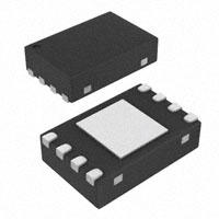
DRF PACKAGE
TOP VIEW
1
4
9
8
5
BOTTOM VIEW
Package Pin Assignments - Numerical Listing
SN65LVDS16, SN65LVP16
8
Z
SN65LVDS17, SN65LVP17
PIN
SIGNAL
PIN
SIGNAL
1
Q
1
Q
2
A
2
A
3
VBB
3
B
4
GC
4
VBB
5
EN
5
EN
6
Z
6
Z
7
Y
7
Y
8
VCC
8
VCC
9
GND
9
GND
�SN65LVDS16, SN65LVP16
SN65LVDS17, SN65LVP17
www.ti.com
SLLS625B – SEPTEMBER 2004 – REVISED NOVEMBER 2005
TYPICAL CHARACTERISTICS
SUPPLY CURRENT
vs
FREQUENCY
SUPPLY CURRENT
vs
FREE-AIR TEMPERATURE
65
I CC − Supply Current − mA
I CC − Supply Current − mA
65
LVP16/17 = Load
55
45
LVDS16/17
35
25
400
800
1200
1600
f − Frequency − MHz
2000
25
−20
0
20
100
LVP16/17 RISE/FALL TIME
vs
FREE-AIR TEMPERATURE
105
97
97
89
tr
81
tf
73
−20
0
20
40
60
80
tf
89
tr
81
73
65
−40
100
−20
0
20
500
4
20
428
Cycle−To−Cycle Jitter − ps
25
Period Jitter − ps
5
tPHL
3
2
1
0
−20
0
20
40
60
80
TA − Free−Air Temperature − C
Figure 11.
100
80
100
CYCLE-TO-CYCLE JITTER
vs
FREQUENCY
524
tPLH
60
Figure 10.
PERIOD JITTER
vs
FREQUENCY
476
40
TA − Free−Air Temperature − C
LVDS16/17
PROPAGATION DELAY TIME
vs
FREE-AIR TEMPERATURE
Propagation Delay Time − ps
80
LVDS16/17 RISE/FALL TIME
vs
FREE-AIR TEMPERATURE
Figure 9.
404
−40
60
Figure 8.
TA − Free−Air Temperature − C
452
40
Figure 7.
105
65
−40
LVDS16/17
35
TA − Free−Air Temperature − C
tr/tf − Rise/Fall Time − ps
tr/tf − Rise/Fall Time − ps
0
45
15
−40
15
LVP16/17 = Load
55
0
400
800
1200
f − Frequency − MHz
Figure 12.
1600
2000
15
10
5
0
0
400
800
1200
1600
2000
f − Frequency − MHz
Figure 13.
9
�SN65LVDS16, SN65LVP16
SN65LVDS17, SN65LVP17
www.ti.com
SLLS625B – SEPTEMBER 2004 – REVISED NOVEMBER 2005
EQUIVALENT INPUT AND OUTPUT SCHEMATIC DIAGRAMS
OUTPUT LVP16/17
OUTPUT LVDS16/17
VCC
R
VCC
VCC
VCC
VCC
R
Y
VCC
Y
7V
Z
Z
7V
7V
7V
ENABLE
VCC
400 Ω
300 kΩ
7V
INPUT
VCC
OUTPUT
VBB
VCC
A
VCC
VCC
B
VBB
10
VBB
�PACKAGE OPTION ADDENDUM
www.ti.com
14-Oct-2022
PACKAGING INFORMATION
Orderable Device
Status
(1)
Package Type Package Pins Package
Drawing
Qty
Eco Plan
(2)
Lead finish/
Ball material
MSL Peak Temp
Op Temp (°C)
Device Marking
(3)
Samples
(4/5)
(6)
SN65LVDS16DRFT
ACTIVE
WSON
DRF
8
250
RoHS & Green
NIPDAU
Level-1-260C-UNLIM
-40 to 85
EL
Samples
SN65LVDS17DRFR
ACTIVE
WSON
DRF
8
3000
RoHS & Green
NIPDAU
Level-1-260C-UNLIM
-40 to 85
EN
Samples
SN65LVDS17DRFT
ACTIVE
WSON
DRF
8
250
RoHS & Green
NIPDAU
Level-1-260C-UNLIM
-40 to 85
EN
Samples
SN65LVP16DRFT
ACTIVE
WSON
DRF
8
250
RoHS & Green
NIPDAU
Level-1-260C-UNLIM
-40 to 85
EK
Samples
SN65LVP17DRFT
ACTIVE
WSON
DRF
8
250
RoHS & Green
NIPDAU
Level-1-260C-UNLIM
-40 to 85
EM
Samples
(1)
The marketing status values are defined as follows:
ACTIVE: Product device recommended for new designs.
LIFEBUY: TI has announced that the device will be discontinued, and a lifetime-buy period is in effect.
NRND: Not recommended for new designs. Device is in production to support existing customers, but TI does not recommend using this part in a new design.
PREVIEW: Device has been announced but is not in production. Samples may or may not be available.
OBSOLETE: TI has discontinued the production of the device.
(2)
RoHS: TI defines "RoHS" to mean semiconductor products that are compliant with the current EU RoHS requirements for all 10 RoHS substances, including the requirement that RoHS substance
do not exceed 0.1% by weight in homogeneous materials. Where designed to be soldered at high temperatures, "RoHS" products are suitable for use in specified lead-free processes. TI may
reference these types of products as "Pb-Free".
RoHS Exempt: TI defines "RoHS Exempt" to mean products that contain lead but are compliant with EU RoHS pursuant to a specific EU RoHS exemption.
Green: TI defines "Green" to mean the content of Chlorine (Cl) and Bromine (Br) based flame retardants meet JS709B low halogen requirements of


 工商网监
湘ICP备2023018690号
工商网监
湘ICP备2023018690号
