SN74ALS232B
16 × 4 ASYNCHRONOUS FIRST-IN, FIRST-OUT MEMORY
SCAS251B – FEBRUARY 1989 – REVISED APRIL 1998
D
D
D
D
D
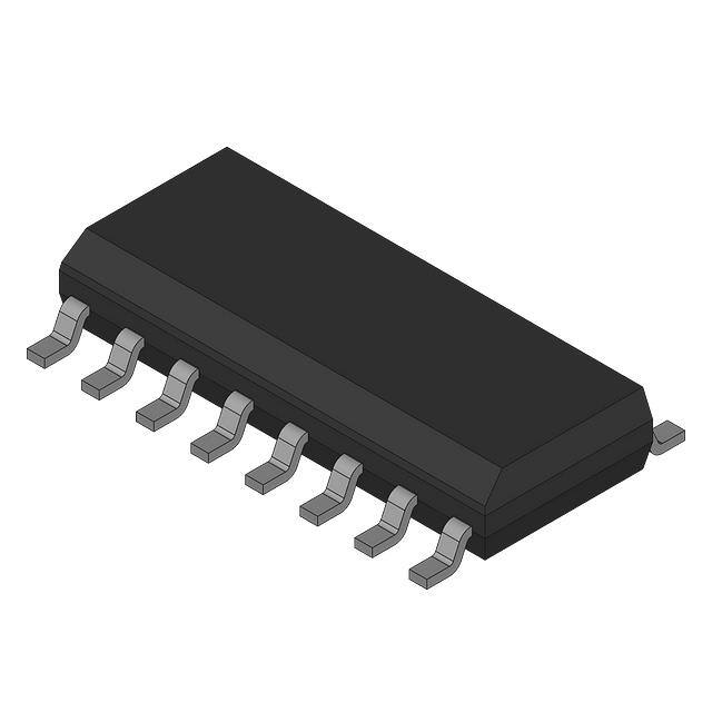
DW OR N PACKAGE
(TOP VIEW)
Independent Asynchronous Inputs and
Outputs
16 Words by 4 Bits
Data Rates up to 40 MHz
Fall-Through Time 14 ns Typical
3-State Outputs
Package Options Include Plastic
Small-Outline Package (DW), Plastic Chip
Carriers (FN), and Standard Plastic 300-mil
DIPs (N)
OE
FULL
LDCK
D0
D1
D2
D3
GND
description
15
3
14
4
13
5
12
6
11
7
10
8
9
VCC
UNCK
EMPTY
Q0
Q1
Q2
Q3
RST
FULL
OE
NC
VCC
UNCK
LDCK
D0
NC
D1
D2
4
3 2 1 20 19
18
5
17
6
16
7
15
8
14
9 10 11 12 13
D3
GND
NC
Data is written into memory on a low-to-high
transition at the load-clock (LDCK) input and is
read out on a low-to-high transition at the
unload-clock (UNCK) input. The memory is full
when the number of words clocked in exceeds by
16 the number of words clocked out. When the
memory is full, LDCK signals have no effect on the
data residing in memory. When the memory is
empty, UNCK signals have no effect.
16
2
FN PACKAGE
(TOP VIEW)
This 64-bit memory features high speed and fast
fall-through times. It is organized as 16 words by
4 bits.
A first-in, first-out (FIFO) memory is a storage
device that allows data to be written into and read
from its array at independent data rates. This
FIFO is designed to process data at rates up to
40 MHz in a bit-parallel format, word by word.
1
EMPTY
Q0
NC
Q1
Q2
RST
Q3
D
NC – No internal connection
Status of the FIFO memory is monitored by the FULL and EMPTY output flags. The FULL output is low when
the memory is full and high when it is not full. The EMPTY output is low when the memory is empty and high
when it is not empty.
A low level on the reset (RST) input resets the internal stack-control pointers and also sets EMPTY low and sets
FULL high. The Q outputs are not reset to any specific logic level. The first low-to-high transition on LDCK, after
either a RST pulse or from an empty condition, causes EMPTY to go high and the data to appear on the
Q outputs. It is important to note that the first word does not have to be unloaded. Data outputs are noninverting
with respect to the data inputs and are at high impedance when the output-enable (OE) input is low. OE does
not affect the FULL or EMPTY output flags. Cascading is easily accomplished in the word-width direction but
is not possible in the word-depth direction.
The SN74ALS232B is characterized for operation from 0°C to 70°C.
Please be aware that an important notice concerning availability, standard warranty, and use in critical applications of
Texas Instruments semiconductor products and disclaimers thereto appears at the end of this data sheet.
Copyright 1998, Texas Instruments Incorporated
PRODUCTION DATA information is current as of publication date.
Products conform to specifications per the terms of Texas Instruments
standard warranty. Production processing does not necessarily include
testing of all parameters.
POST OFFICE BOX 655303
• DALLAS, TEXAS 75265
1
�SN74ALS232B
16 × 4 ASYNCHRONOUS FIRST-IN, FIRST-OUT MEMORY
SCAS251B – FEBRUARY 1989 – REVISED APRIL 1998
logic symbol†
FIFO 16 × 4
RST
LDCK
UNCK
OE
D0
D1
D2
D3
9
3
15
CTR
CT = 0
1(+/C2)
(CT = 16) G1
(CT = 0) G3
2
14
FULL
EMPTY
3–
1
4
5
EN4
2D
4
13
12
6
11
7
10
Q0
Q1
Q2
Q3
† This symbol is in accordance with ANSI/IEEE Standard 91-1984 and IEC Publication 617-12. The symbol is functionally accurate but does
not show the details of implementation; for these, see the logic diagram. The symbol represents the memory as if it were controlled by a single
counter whose content is the number of words stored at the time. Output data is invalid when the counter content (CT) is 0.
Pin numbers shown are for the DW and N packages.
2
POST OFFICE BOX 655303
• DALLAS, TEXAS 75265
�SN74ALS232B
16 × 4 ASYNCHRONOUS FIRST-IN, FIRST-OUT MEMORY
SCAS251B – FEBRUARY 1989 – REVISED APRIL 1998
logic diagram (positive logic)
1
OE
Ring
Counter
CTR
DIV 16
1D
3
C1
LDCK
S
R
C2
2D
RST
Ring
Counter
CTR
DIV 16
1
2
3
4
5
6
7
8
+
9
10
Read
11
Address 12
13
14
CT = 1
15
16
15
UNCK
1
2
3
4
5
6
7
8
+
9
10
Write 11
Address 12
13
14
CT = 1
15
16
9
16
RAM 16 × 4
EN
16
16
1A
1
16
2A
1
16
C3
D0
D1
D2
D3
16
4
1A, 3D
5
2A
13
12
6
11
7
10
16
COMP
P=Q
Q1
Q2
Q3
14
P
Q
Q0
EMPTY
S
P= Q+1
2
P = Q–1
R
FULL
Pin numbers shown are for the DW and N packages.
POST OFFICE BOX 655303
• DALLAS, TEXAS 75265
3
�SN74ALS232B
16 × 4 ASYNCHRONOUS FIRST-IN, FIRST-OUT MEMORY
SCAS251B – FEBRUARY 1989 – REVISED APRIL 1998
timing diagram
RST
LDCK
D0–D3
ÎÎÎÎÎÎ
ÎÎÎÎÎÎÎÎÎÎ
ÎÎÎÎÎÎÎÎÎÎÎÎÎÎÎ
ÎÎÎÎÎÎ
ÎÎÎÎÎÎÎÎÎÎ
ÎÎÎÎÎÎÎÎÎÎÎÎÎÎÎ
ÎÎÎ
ÎÎÎÎ
ÎÎÎ
ÎÎÎÎ
ÎÎÎ
ÎÎÎÎ
Don’t Care
W1
UNCK
Q0–Q3 Invalid
W2
W3
W1
Word 1
Invalid
W2
W15 W16
Word 1
Word 2 Word 3
EMPTY
Word 2 Word 3 Word 4
FULL
Load
W1
Initialize
Pointers
Unload
W2
Empty
Full
absolute maximum ratings over operating free-air temperature range (unless otherwise noted)†
Supply voltage range, VCC . . . . . . . . . . . . . . . . . . . . . . . . . . . . . . . . . . . . . . . . . . . . . . . . . . . . . . . . . . –0.5 V to 7 V
Input voltage range, VI . . . . . . . . . . . . . . . . . . . . . . . . . . . . . . . . . . . . . . . . . . . . . . . . . . . . . . . . . . . . . . –0.5 V to 7 V
Voltage range applied to a disabled 3-state output . . . . . . . . . . . . . . . . . . . . . . . . . . . . . . . . . . . . . –0.5 V to 5.5 V
Package thermal impedance, θJA (see Note 2): DW package . . . . . . . . . . . . . . . . . . . . . . . . . . . . . . . . 105°C/W
FN package . . . . . . . . . . . . . . . . . . . . . . . . . . . . . . . . . 83°C/W
N package . . . . . . . . . . . . . . . . . . . . . . . . . . . . . . . . . . . 78°C/W
Storage temperature range, Tstg . . . . . . . . . . . . . . . . . . . . . . . . . . . . . . . . . . . . . . . . . . . . . . . . . . . –65°C to 150°C
† Stresses beyond those listed under “absolute maximum ratings” may cause permanent damage to the device. This is a stress rating only, and
functional operation of the device at these or any other conditions beyond those indicated in the “recommended operating conditions” section of
this specification is not implied. Exposure to absolute-maximum-rated conditions for extended periods may affect device reliability.
NOTES: 1. All voltage values are with respect to GND.
2. The package thermal impedance is calculated in accordance with JESD 51, except for through-hole packages, which use a trace
length of zero.
4
POST OFFICE BOX 655303
• DALLAS, TEXAS 75265
�SN74ALS232B
16 × 4 ASYNCHRONOUS FIRST-IN, FIRST-OUT MEMORY
SCAS251B – FEBRUARY 1989 – REVISED APRIL 1998
recommended operating conditions (see Note 3)
VCC
VIH
Supply voltage
VIL
Low-level input voltage
IOH
High level output current
High-level
IOL
Low level output current
Low-level
High-level input voltage
MIN
NOM
MAX
4.5
5
5.5
2
UNIT
V
V
0.8
Q outputs
–2.6
FULL, EMPTY
–0.4
Q outputs
24
FULL, EMPTY
8
V
mA
mA
TA
Operating free-air temperature
0
70
°C
NOTE 3: To ensure proper operation of this high-speed FIFO device, it is necessary to provide a clean signal to the LDCK and UNCK clock inputs.
Any excessive noise or glitching on the clock inputs that violates limits for maximum VIL, minimum VIH, or minimum pulse duration can
cause a false clock or improper operation of the internal read and write pointers.
electrical characteristics over recommended operating free-air temperature range (unless
otherwise noted)
PARAMETER
VIK
VOH
TEST CONDITIONS
Q outputs
VCC = 4.5 V,
VCC = 4.5 V,
II = –18 mA
IOH = –2.6 mA
FULL, EMPTY
VCC = 4.5 V to 5.5 V,
Q outputs
VCC = 4
4.5
5V
IOH = –0.4 mA
IOL = 12 mA
FULL EMPTY
FULL,
VCC = 4
4.5
5V
VOL
IOZH
IOZL
VCC = 5.5 V,
VCC = 5.5 V,
II
IIH
VCC = 5.5 V,
VCC = 5.5 V,
IIL
IO‡
VCC = 5.5 V,
VCC = 5.5 V,
MIN
TYP†
2.4
3.2
MAX
UNIT
–1.2
V
V
VCC–2
0.25
0.4
IOL = 24 mA
IOL = 4 mA
0.35
0.5
0.25
0.4
IOL = 8 mA
VO = 2.7 V
0.35
0.5
20
VO = 0.4 V
VI = 7 V
VI = 2.7 V
VI = 0.4 V
VO = 2.25 V
–30
V
µA
–20
µA
0.1
mA
20
µA
–0.2
mA
–112
mA
ICC
VCC = 5.5 V
80
125
mA
† All typical values are at VCC = 5 V, TA = 25°C.
‡ The output conditions have been chosen to produce a current that closely approximates one-half of the true short-circuit output current, IOS.
POST OFFICE BOX 655303
• DALLAS, TEXAS 75265
5
�SN74ALS232B
16 × 4 ASYNCHRONOUS FIRST-IN, FIRST-OUT MEMORY
SCAS251B – FEBRUARY 1989 – REVISED APRIL 1998
timing requirements over recommended operating free-air temperature range (see Figure 1)
MIN
fclock†
tw
Clock frequency
Pulse duration
tsu
Setup time
th
Hold time
NOM
MAX
LDCK
40
UNCK
40
RST low
18
LDCK low
15
LDCK high
10
UNCK low
15
UNCK high
10
Data before LDCK↑
8
LDCK inactive before RST↑
5
Data after LDCK↑
5
LDCK inactive after RST↑
5
UNIT
MHz
ns
ns
ns
† The maximum possible clock frequency is 40 MHz. The maximum clock frequency when using a 50% duty cycle is 33.3 MHz.
switching characteristics (see Figure 1)
PARAMETER
FROM
(INPUT)
fmax
LDCK, UNCK
50
LDCK↑
14
23
6
30
15
23
6
30
13
20
5
25
15
22
6
27
15
21
5
26
15
22
6
27
13
20
5
25
16
23
7
28
tpd
d
tPLH
TO
(OUTPUT)
UNCK↑
LDCK↑
Any Q
EMPTY
UNCK↑
tPHL
EMPTY
RST↓
LDCK↑
tPLH
FULL
UNCK↑
ten
tdis
FULL
RST↓
TYP‡
MAX
MIN
MAX
40
UNIT
MHz
ns
ns
ns
ns
OE↑
Q
5
12
1
14
ns
OE↓
Q
5
12
1
16
ns
‡ Typical values at VCC – 5 V, TA = 25°C.
6
MIN
POST OFFICE BOX 655303
• DALLAS, TEXAS 75265
�SN74ALS232B
16 × 4 ASYNCHRONOUS FIRST-IN, FIRST-OUT MEMORY
SCAS251B – FEBRUARY 1989 – REVISED APRIL 1998
PARAMETER MEASUREMENT INFORMATION
7V
SWITCH POSITION TABLE
PARAMETER
Open
S1
ten
R1 = 500 Ω
From Output
Under Test
CL = 50 pF
(see Note A)
tdis
Test Point
tpd
R2 = 500 Ω
LOAD CIRCUIT FOR 3-STATE OUTPUTS
Open
Closed
Open
Closed
Open
Open
3.5 V
High-Level
Pulse
1.3 V
1.3 V
0.3 V
tw
3.5 V
Timing
Input
S1
tPZH
tPZL
tPHZ
tPLZ
tPLH
tPHL
3.5 V
1.3 V
0.3 V
th
tsu
Low-Level
Pulse
3.5 V
Data
Input
1.3 V
1.3 V
1.3 V
0.3 V
VOLTAGE WAVEFORMS
PULSE DURATION
1.3 V
0.3 V
VOLTAGE WAVEFORMS
SETUP AND HOLD TIMES
3.5 V
Output
Control
1.3 V
1.3 V
0.3 V
3.5 V
Input
(see Note C)
1.3 V
tPZL
1.3 V
tPLZ
0.3 V
tPLH
tPHL
VOH
In-Phase
Output
1.3 V
1.3 V
1.3 V
VOL
tPHL
Out-of-Phase
Output
3.5 V
Waveform 1
S1 Closed
(see Note B)
tPZH
tPLH
VOH
1.3 V
1.3 V
VOL
VOLTAGE WAVEFORMS
PROPAGATION DELAY TIMES
Waveform 2
S1 Open
(see Note B)
tPHZ
VOL
0.3 V
VOH
1.3 V
0.3 V
0V
VOLTAGE WAVEFORMS
ENABLE AND DISABLE TIMES, 3-STATE OUTPUTS
NOTES: A. CL includes probe and jig capacitance.
B. Waveform 1 is for an output with internal conditions such that the output is low except when disabled by the output control.
Waveform 2 is for an output with internal conditions such that the output is high except when disabled by the output control.
C. All input pulses are supplied by generators having the following characteristics: PRR ≤ 1 MHz, Zo = 50 Ω, tr ≤ 2 ns, tf ≤ 2 ns.
D. The outputs are measured one at a time with one transition per measurement.
Figure 1. Load Circuit and Voltage Waveforms
POST OFFICE BOX 655303
• DALLAS, TEXAS 75265
7
�PACKAGE OPTION ADDENDUM
www.ti.com
10-Dec-2020
PACKAGING INFORMATION
Orderable Device
Status
(1)
Package Type Package Pins Package
Drawing
Qty
Eco Plan
(2)
Lead finish/
Ball material
MSL Peak Temp
Op Temp (°C)
Device Marking
(3)
(4/5)
(6)
SN74ALS232BDW
ACTIVE
SOIC
DW
16
40
RoHS & Green
NIPDAU
Level-1-260C-UNLIM
0 to 70
ALS232B
SN74ALS232BN
ACTIVE
PDIP
N
16
25
RoHS &
Non-Green
NIPDAU
N / A for Pkg Type
0 to 70
SN74ALS232BN
(1)
The marketing status values are defined as follows:
ACTIVE: Product device recommended for new designs.
LIFEBUY: TI has announced that the device will be discontinued, and a lifetime-buy period is in effect.
NRND: Not recommended for new designs. Device is in production to support existing customers, but TI does not recommend using this part in a new design.
PREVIEW: Device has been announced but is not in production. Samples may or may not be available.
OBSOLETE: TI has discontinued the production of the device.
(2)
RoHS: TI defines "RoHS" to mean semiconductor products that are compliant with the current EU RoHS requirements for all 10 RoHS substances, including the requirement that RoHS substance
do not exceed 0.1% by weight in homogeneous materials. Where designed to be soldered at high temperatures, "RoHS" products are suitable for use in specified lead-free processes. TI may
reference these types of products as "Pb-Free".
RoHS Exempt: TI defines "RoHS Exempt" to mean products that contain lead but are compliant with EU RoHS pursuant to a specific EU RoHS exemption.
Green: TI defines "Green" to mean the content of Chlorine (Cl) and Bromine (Br) based flame retardants meet JS709B low halogen requirements of


 工商网监
湘ICP备2023018690号
工商网监
湘ICP备2023018690号
