SN74CBT6800
10-BIT FET BUS SWITCH
WITH PRECHARGED OUTPUTS FOR LIVE INSERTION
SCDS005J – MARCH 1993 – REVISED DECEMBER 1998
D
D
D
D
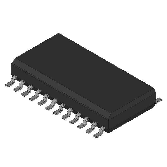
DB, DBQ, DW, OR PW PACKAGE
(TOP VIEW)
5-Ω Switch Connection Between Two Ports
TTL-Compatible Input Levels
Outputs Are Precharged by Bias Voltage to
Minimize Signal Distortion During Live
Insertion
Package Options Include Plastic Shrink
Small-Outline (DB, DBQ), Small-Outline
(DW), and Thin Shrink Small-Outline (PW)
Packages
ON
A1
A2
A3
A4
A5
A6
A7
A8
A9
A10
GND
description
The SN74CBT6800 provides ten bits of
high-speed TTL-compatible bus switching. The
low on-state resistance of the switch allows
bidirectional connections to be made while adding
near-zero propagation delay. The device also
precharges the B port to a user-selectable bias
voltage (BIASV) to minimize live-insertion noise.
1
24
2
23
3
22
4
21
5
20
6
19
7
18
8
17
9
16
10
15
11
14
12
13
VCC
B1
B2
B3
B4
B5
B6
B7
B8
B9
B10
BIASV
The SN74CBT6800 is organized as one 10-bit switch with a single enable (ON) input. When ON is low, the
switch is on and port A is connected to port B. When ON is high, the switch between port A and port B is open
and the B port is precharged to BIASV through the equivalent of a 10-kΩ resistor.
The SN74CBT6800 is characterized for operation from –40°C to 85°C.
FUNCTION TABLE
ON
B1–B10
FUNCTION
L
A1–A10
Connect
H
BIASV
Precharge
logic diagram (positive logic)
13
BIASV
2
23
A1
B1
11
14
A10
B10
1
ON
Please be aware that an important notice concerning availability, standard warranty, and use in critical applications of
Texas Instruments semiconductor products and disclaimers thereto appears at the end of this data sheet.
Copyright 1998, Texas Instruments Incorporated
PRODUCTION DATA information is current as of publication date.
Products conform to specifications per the terms of Texas Instruments
standard warranty. Production processing does not necessarily include
testing of all parameters.
POST OFFICE BOX 655303
• DALLAS, TEXAS 75265
1
�SN74CBT6800
10-BIT FET BUS SWITCH
WITH PRECHARGED OUTPUTS FOR LIVE INSERTION
SCDS005J – MARCH 1993 – REVISED DECEMBER 1998
absolute maximum ratings over operating free-air temperature range (unless otherwise noted)†
Supply voltage range, VCC . . . . . . . . . . . . . . . . . . . . . . . . . . . . . . . . . . . . . . . . . . . . . . . . . . . . . . . . . . –0.5 V to 7 V
Bias voltage range, BIASV . . . . . . . . . . . . . . . . . . . . . . . . . . . . . . . . . . . . . . . . . . . . . . . . . . . . . . . . . . –0.5 V to 7 V
Input voltage range, VI (see Note 1) . . . . . . . . . . . . . . . . . . . . . . . . . . . . . . . . . . . . . . . . . . . . . . . . . . –0.5 V to 7 V
Continuous channel current . . . . . . . . . . . . . . . . . . . . . . . . . . . . . . . . . . . . . . . . . . . . . . . . . . . . . . . . . . . . . . 128 mA
Input clamp current, IIK (VI < 0) . . . . . . . . . . . . . . . . . . . . . . . . . . . . . . . . . . . . . . . . . . . . . . . . . . . . . . . . . . . –50 mA
Package thermal impedance, θJA (see Note 2): DB package . . . . . . . . . . . . . . . . . . . . . . . . . . . . . . . . 104°C/W
DBQ package . . . . . . . . . . . . . . . . . . . . . . . . . . . . . . . 103°C/W
DW package . . . . . . . . . . . . . . . . . . . . . . . . . . . . . . . . . 81°C/W
PW package . . . . . . . . . . . . . . . . . . . . . . . . . . . . . . . . 120°C/W
Storage temperature range, Tstg . . . . . . . . . . . . . . . . . . . . . . . . . . . . . . . . . . . . . . . . . . . . . . . . . . . –65°C to 150°C
† Stresses beyond those listed under “absolute maximum ratings” may cause permanent damage to the device. These are stress ratings only, and
functional operation of the device at these or any other conditions beyond those indicated under “recommended operating conditions” is not
implied. Exposure to absolute-maximum-rated conditions for extended periods may affect device reliability.
NOTES: 1. The input and output negative-voltage ratings may be exceeded if the input and output clamp-current ratings are observed.
2. The package thermal impedance is calculated in accordance with JESD 51.
recommended operating conditions (see Note 3)
MIN
MAX
UNIT
VCC
BIASV
Supply voltage
4
5.5
V
Supply voltage
1.3
VCC
V
VIH
VIL
High-level control input voltage
2
Low-level control input voltage
V
0.8
V
TA
Operating free-air temperature
–40
85
°C
NOTE 3: All unused control inputs of the device must be held at VCC or GND to ensure proper device operation. Refer to the TI application report,
Implications of Slow or Floating CMOS Inputs, literature number SCBA004.
electrical characteristics over recommended operating free-air temperature range (unless
otherwise noted)
PARAMETER
TEST CONDITIONS
VIK
II
VCC = 4.5 V,
VCC = 5.5 V,
II = –18 mA
VI = 5.5 V or GND
IO
ICC
VCC = 4.5 V,
VCC = 5.5 V,
BIASV = 2.4 V,
∆ICC§
Ci
Co(OFF)
Control inputs
Control inputs
VCC = 3.6 V,
VI = 3 V or 0
IO = 0,
One input at 2.7 V,
MIN
TYP‡
MAX
UNIT
–1.2
V
±5
VO= 0
VI = VCC or GND
0.25
Other inputs at VCC or GND
50
µA
2.5
mA
3.5
pF
4.5
pF
VO = 3 V or 0,
Switch off
VCC = 4 V,
TYP at VCC = 4 V
VI = 2.4 V,
II = 15 mA
14
20
VI = 0
II = 64 mA
II = 30 mA
5
7
5
7
ron¶
VCC = 4.5 V
µA
mA
Ω
VI = 2.4 V,
II = 15 mA
10
15
‡ All typical values are at VCC = 5 V (unless otherwise noted), TA = 25°C.
§ This is the increase in supply current for each input that is at the specified TTL voltage level rather than VCC or GND.
¶ Measured by the voltage drop between the A and B terminals at the indicated current through the switch. On-state resistance is determined by
the lower of the voltages of the two (A or B) terminals.
2
POST OFFICE BOX 655303
• DALLAS, TEXAS 75265
�SN74CBT6800
10-BIT FET BUS SWITCH
WITH PRECHARGED OUTPUTS FOR LIVE INSERTION
SCDS005J – MARCH 1993 – REVISED DECEMBER 1998
switching characteristics over recommended operating free-air temperature range, CL = 50 pF
(unless otherwise noted) (see Figure 1)
TEST
CONDITIONS
PARAMETER
tpd†
tPZH
BIASV = GND
tPZL
BIASV = 3 V
tPHZ
BIASV = GND
tPLZ
BIASV = 3 V
FROM
(INPUT)
TO
(OUTPUT)
A or B
B or A
ON
A or B
ON
A or B
VCC = 4 V
VCC = 5 V
± 0.5 V
MIN
MIN
MAX
UNIT
MAX
0.35
0.25
9.1
3.1
8.1
9.6
3.6
8.6
5.9
2.7
6.1
6.4
3
7.3
ns
ns
ns
† The propagation delay is the calculated RC time constant of the typical on-state resistance of the switch and the specified load capacitance, when
driven by an ideal voltage source (zero output impedance).
PARAMETER MEASUREMENT INFORMATION
7V
S1
500 Ω
From Output
Under Test
Open
GND
CL = 50 pF
(see Note A)
500 Ω
TEST
S1
tpd
tPLZ/tPZL
tPHZ/tPZH
Open
7V
Open
Output
Control
(low-level
enabling)
LOAD CIRCUIT
3V
1.5 V
0V
tPZL
3V
Input
1.5 V
1.5 V
0V
tPLH
1.5 V
1.5 V
VOL
tPLZ
3.5 V
1.5 V
tPZH
VOH
Output
Output
Waveform 1
S1 at 7 V
(see Note B)
tPHL
1.5 V
Output
Waveform 2
S1 at Open
(see Note B)
VOLTAGE WAVEFORMS
PROPAGATION DELAY TIMES
VOL + 0.3 V
VOL
tPHZ
1.5 V
VOH
VOH – 0.3 V
0V
VOLTAGE WAVEFORMS
ENABLE AND DISABLE TIMES
NOTES: A. CL includes probe and jig capacitance.
B. Waveform 1 is for an output with internal conditions such that the output is low except when disabled by the output control.
Waveform 2 is for an output with internal conditions such that the output is high except when disabled by the output control.
C. All input pulses are supplied by generators having the following characteristics: PRR ≤ 10 MHz, ZO = 50 Ω, tr ≤ 2.5 ns, tf ≤ 2.5 ns.
D. The outputs are measured one at a time with one transition per measurement.
E. tPLZ and tPHZ are the same as tdis.
F. tPZL and tPZH are the same as ten.
G. tPLH and tPHL are the same as tpd.
Figure 1. Load Circuit and Voltage Waveforms
POST OFFICE BOX 655303
• DALLAS, TEXAS 75265
3
�IMPORTANT NOTICE
Texas Instruments and its subsidiaries (TI) reserve the right to make changes to their products or to discontinue
any product or service without notice, and advise customers to obtain the latest version of relevant information
to verify, before placing orders, that information being relied on is current and complete. All products are sold
subject to the terms and conditions of sale supplied at the time of order acknowledgment, including those
pertaining to warranty, patent infringement, and limitation of liability.
TI warrants performance of its semiconductor products to the specifications applicable at the time of sale in
accordance with TI’s standard warranty. Testing and other quality control techniques are utilized to the extent
TI deems necessary to support this warranty. Specific testing of all parameters of each device is not necessarily
performed, except those mandated by government requirements.
Customers are responsible for their applications using TI components.
In order to minimize risks associated with the customer’s applications, adequate design and operating
safeguards must be provided by the customer to minimize inherent or procedural hazards.
TI assumes no liability for applications assistance or customer product design. TI does not warrant or represent
that any license, either express or implied, is granted under any patent right, copyright, mask work right, or other
intellectual property right of TI covering or relating to any combination, machine, or process in which such
semiconductor products or services might be or are used. TI’s publication of information regarding any third
party’s products or services does not constitute TI’s approval, warranty or endorsement thereof.
Copyright 2000, Texas Instruments Incorporated
�1 of 3
Products
Development Tools
Applications
Search
PRODUCT FOLDER | PRODUCT INFO: FEATURES | DESCRIPTION | DATASHEETS |
PRICING/AVAILABILITY | SAMPLES |
APPLICATION NOTES | RELATED DOCUMENTS
PRODUCT SUPPORT: TRAINING
SN74CBT6800, 10-Bit FET Bus Switch With Precharged Outputs For Live Insertion
DEVICE STATUS: ACTIVE
PARAMETER NAME SN74CBT6800
Voltage Nodes (V) 5
Vcc range (V)
4.0 to 5.5
No. of Bits
10
ron(max) (ohms)
7
tpd(max) (ns)
0.25
FEATURES
l
l
l
l
Back to Top
5- Switch Connection Between Two Ports
TTL-Compatible Input Levels
Outputs Are Precharged by Bias Voltage to Minimize Signal Distortion During Live
Insertion
Package Options Include Plastic Shrink Small-Outline (DB, DBQ), Small-Outline (DW),
and Thin Shrink Small-Outline (PW) Packages
DESCRIPTION
Back to Top
The SN74CBT6800 provides ten bits of high-speed TTL-compatible bus switching. The low onstate resistance of the switch allows bidirectional connections to be made while adding nearzero propagation delay. The device also precharges the B port to a user-selectable bias
voltage (BIASV) to minimize live-insertion noise.
The SN74CBT6800 is organized as one 10-bit switch with a single enable (ON\) input. When
ON\ is low, the switch is on and port A is connected to port B. When ON\ is high, the switch
between port A and port B is open and the B port is precharged to BIASV through the
equivalent of a 10-k resistor.
The SN74CBT6800 is characterized for operation from -40°C to 85°C.
TECHNICAL DOCUMENTS
Back to Top
�2 of 3
To view the following documents, Acrobat Reader 3.x is required.
To download a document to your hard drive, right-click on the link and choose 'Save'.
Back to Top
DATASHEET
Full datasheet in Acrobat PDF: scds005j.pdf (61 KB) ( Updated: 12/14/1998)
Full datasheet in Zipped PostScript: scds005j.psz (61 KB)
Back to Top
APPLICATION NOTES
View Application Reports for Digital Logic
l
l
l
l
l
l
l
l
l
l
5-V To 3.3-V Translation With The SN74CBTD3384 (SCDA003B - Updated: 03/01/1997)
Flexible Voltage-Level Translation With CBT Family Devices (SCDA006 - Updated:
07/20/1999)
Implications of Slow or Floating CMOS Inputs (SCBA004C - Updated: 02/01/1998)
Low-Voltage Bus-Switch Technology And Applications (SCDA005 - Updated: 12/01/1997)
Migration From 3.3-V To 2.5-V Power Supplies For Logic Devices (SCEA005 - Updated:
12/01/1997)
SN74CBTS3384 Bus Switches Provide Fast Connection And Ensure Isolation (SCDA002A Updated: 08/01/1996)
TI Logic Solutions for Memory Interleaving With the Intel440BX Chipset (SCCA001 Updated: 04/08/1999)
Texas Instruments Crossbar Switches (SCDA001A - Updated: 06/01/1995)
Texas Instruments Solution for Undershoot Protection for Bus Switches (SCDA007 Updated: 04/13/2000)
Understanding Advanced Bus-Interface Products Design Guide (SCAA029, 253 KB Updated: 05/01/1996)
Back to Top
RELATED DOCUMENTS
l
l
l
l
Documentation Rules (SAP) And Ordering Information (SZZU001B, 4 KB - Updated:
05/06/1999)
Logic Selection Guide Second Half 2000 (SDYU001N, 5035 KB - Updated: 04/17/2000)
MicroStar Junior BGA Design Summary (SCET004, 167 KB - Updated: 07/28/2000)
More Power In Less Space - Technical Article (SCAU001A, 850 KB - Updated: 03/01/1996)
Back to Top
SAMPLES
ORDERABLE DEVICE
PACKAGE
PINS
TEMP (ºC)
STATUS
SAMPLES
SN74CBT6800DW
DW
24
-40 TO 85
ACTIVE
Request Samples
SN74CBT6800PWLE
PW
24
-40 TO 85
OBSOLETE
Back to Top
PRICING/AVAILABILITY
ORDERABLE
DEVICE
PACKAGE PINS
TEMP
(ºC)
STATUS
SN74CBT6800DBLE
DB
24
-40 TO
85
OBSOLETE
SN74CBT6800DBQR
DBQ
24
-40 TO
85
ACTIVE
BUDGETARY
PRICE
US$/UNIT
QTY=1000+
PACK
QTY
PRICING/AVAILABILITY
1.09
2500
Check stock or order
�3 of 3
SN74CBT6800DBR
DB
24
-40 TO
85
ACTIVE
1.09
2000
Check stock or order
SN74CBT6800DGVR
DGV
24
-40 TO
85
ACTIVE
1.25
2000
Check stock or order
SN74CBT6800DW
DW
24
-40 TO
85
ACTIVE
1.09
25
Check stock or order
SN74CBT6800DWR
DW
24
-40 TO
85
ACTIVE
1.15
2000
Check stock or order
SN74CBT6800PWLE
PW
24
-40 TO
85
OBSOLETE
SN74CBT6800PWR
PW
24
-40 TO
85
ACTIVE
1.09
2000
Check stock or order
Table Data Updated on: 11/15/2000
© Copyright 2000 Texas Instruments Incorporated. All rights reserved. Trademarks | Privacy Policy
| Important Notice
�


 工商网监
湘ICP备2023018690号
工商网监
湘ICP备2023018690号
