SN74F574
OCTAL EDGE-TRIGGERED D-TYPE FLIP-FLOP
WITH 3-STATE OUTPUTS
SDFS005A – D3034, SEPTEMBER 1987 – REVISED OCTOBER 1993
•
•
•
•
•
DW OR N PACKAGE
(TOP VIEW)
Eight D-Type Flip-Flops in a Single
Package
3-State Bus-Driving True Outputs
Full Parallel Access for Loading
Buffered Control Inputs
Package Options Include Plastic
Small-Outline Packages and Standard
Plastic 300-mil DIPs
OE
1D
2D
3D
4D
5D
6D
7D
8D
GND
description
This 8-bit flip-flop features 3-state outputs
designed specifically for driving highly capacitive
or relatively low-impedance loads. It is particularly
suitable for implementing buffer registers, I/O
ports, bidirectional bus drivers, and working
registers.
1
20
2
19
3
18
4
17
5
16
6
15
7
14
8
13
9
12
10
11
VCC
1Q
2Q
3Q
4Q
5Q
6Q
7Q
8Q
CLK
The eight flip-flops of the SN74F574 are edge-triggered D-type flip-flops. On the positive transition of the clock
(CLK) input, the Q outputs will be set to the logic levels that were set up at the data (D) inputs.
A buffered output enable (OE) input can be used to place the eight outputs in either a normal logic state (high
or low logic levels) or a high-impedance state. In the high-impedance state, the outputs neither load nor drive
the bus lines significantly. The high-impedance state and increased drive provide the capability to drive bus
lines without need for interface or pullup components.
The output enable (OE) does not affect the internal operations of the flip-flops. Old data can be retained or new
data can be entered while the outputs are in the high-impedance state.
The SN74F574 is characterized for operation from 0°C to 70°C.
FUNCTION TABLE
(each flip-flop)
INPUTS
OE
CLK
D
OUTPUT
Q
L
↑
H
H
L
↑
L
L
L
L
X
Q0
H
X
X
Z
Copyright 1993, Texas Instruments Incorporated
PRODUCTION DATA information is current as of publication date.
Products conform to specifications per the terms of Texas Instruments
standard warranty. Production processing does not necessarily include
testing of all parameters.
POST OFFICE BOX 655303
• DALLAS, TEXAS 75265
2–1
�SN74F574
OCTAL EDGE-TRIGGERED D-TYPE FLIP-FLOP
WITH 3-STATE OUTPUTS
SDFS005A – D3034, SEPTEMBER 1987 – REVISED OCTOBER 1993
logic symbol†
OE
CLK
1D
2D
3D
4D
5D
6D
7D
8D
1
11
2
logic diagram (positive logic)
EN
OE
C1
19
1D
3
18
4
17
5
16
6
15
7
14
8
13
9
12
CLK
1
11
1Q
C1
2Q
3Q
1D
2
19
1Q
1D
4Q
5Q
6Q
7Q
To Seven Other Channels
8Q
† This symbol is in accordance with ANSI/IEEE Std 91-1984 and
IEC Publication 617-12.
absolute maximum ratings over operating free-air temperature range (unless otherwise noted)‡
Supply voltage range, VCC . . . . . . . . . . . . . . . . . . . . . . . . . . . . . . . . . . . . . . . . . . . . . . . . . . . . . . . . . . – 0.5 V to 7 V
Input voltage range, VI (see Note 1) . . . . . . . . . . . . . . . . . . . . . . . . . . . . . . . . . . . . . . . . . . . . . . . . . . . – 1.2 V to 7 V
Input current range . . . . . . . . . . . . . . . . . . . . . . . . . . . . . . . . . . . . . . . . . . . . . . . . . . . . . . . . . . . . . . . – 30 mA to 5 mA
Voltage range applied to any output in the disabled or power-off state . . . . . . . . . . . . . . . . . . . . – 0.5 V to 5.5 V
Voltage range applied to any output in the high state . . . . . . . . . . . . . . . . . . . . . . . . . . . . . . . . . . . – 0.5 V to VCC
Current into any output in the low state . . . . . . . . . . . . . . . . . . . . . . . . . . . . . . . . . . . . . . . . . . . . . . . . . . . . . . 48 mA
Operating free-air temperature range . . . . . . . . . . . . . . . . . . . . . . . . . . . . . . . . . . . . . . . . . . . . . . . . . . . 0°C to 70°C
Storage temperature range . . . . . . . . . . . . . . . . . . . . . . . . . . . . . . . . . . . . . . . . . . . . . . . . . . . . . . . . – 65°C to 150°C
‡ Stresses beyond those listed under “absolute maximum ratings” may cause permanent damage to the device. These are stress ratings only, and
functional operation of the device at these or any other conditions beyond those indicated under “recommended operating conditions” is not
implied. Exposure to absolute-maximum-rated conditions for extended periods may affect device reliability.
NOTE 1: The input-voltage ratings may be exceeded provided the input-current ratings are observed.
recommended operating conditions
VCC
VIH
Supply voltage
VIL
IIK
Low-level input voltage
IOH
IOL
High-level output current
TA
Operating free-air temperature
2–2
High-level input voltage
MIN
NOM
MAX
4.5
5
5.5
2
Input clamp current
Low-level output current
0
POST OFFICE BOX 655303
• DALLAS, TEXAS 75265
UNIT
V
V
0.8
V
– 18
mA
–3
mA
24
mA
70
°C
�SN74F574
OCTAL EDGE-TRIGGERED D-TYPE FLIP-FLOP
WITH 3-STATE OUTPUTS
SDFS005A – D3034, SEPTEMBER 1987 – REVISED OCTOBER 1993
electrical characteristics over recommended operating free-air temperature range (unless
otherwise noted)
PARAMETER
TEST CONDITIONS
VIK
VCC = 4.5 V,
II = – 18 mA
IOH = – 1 mA
VCC = 4
4.5
5V
VOH
IOH = – 3 mA
IOH = – 1 mA to – 3 mA
VCC = 4.75 V,
VCC = 4.5 V,
VOL
IOZH
3.4
2.4
3.3
MAX
UNIT
– 1.2
V
V
2.7
0.35
VI = 2.7 V
VI = 0.5 V
VCC = 5.5 V,
VCC = 5.5 V,
IOS‡
ICCZ
2.5
VO = 0.5 V
VI = 7 V
VCC = 5.5 V,
VCC = 5.5 V,
IIH
IIL
TYP†
IOL = 24 mA
VO = 2.7 V
VCC = 5.5 V,
VCC = 5.5 V,
IOZL
II
MIN
VO = 0
See Note 2
– 60
0.5
V
50
µA
– 50
µA
0.1
mA
20
µA
– 0.6
mA
– 150
mA
86
mA
VCC = 5.5 V,
55
† All typical values are at VCC = 5 V, TA = 25°C.
‡ Not more than one output should be shorted at a time, and the duration of the short circuit should not exceed one second.
NOTE 2: ICCZ is measured with OE at 4.5 V and all other inputs grounded.
timing requirements
VCC = 5 V,
TA = 25°C
fclock
Clock frequency
tw
Pulse duration
tsu
Setup time before CLK↑
th
Hold time after CLK↑
VCC = 4.5 V to 5.5 V,
TA = MIN to MAX§
MIN
MAX
MIN
MAX
0
100
0
100
CLK high
7
7
CLK low
6
6
Data high
2
2
Data low
2
2
Data high
2
2
Data low
2
2
UNIT
MHz
ns
ns
ns
switching characteristics (see Note 3)
PARAMETER
FROM
(INPUT)
TO
(OUTPUT)
VCC = 5 V,
CL = 50 pF,
RL = 500 Ω,
TA = 25°C
MIN
fmax
tPLH
tPHL
tPZH
tPZL
tPHZ
TYP
VCC = 4.5 V to 5.5 V,
CL = 50 pF,
RL = 500 Ω,
TA = MIN to MAX §
MAX
100
CLK
Any Q
OE
Any Q
MIN
POST OFFICE BOX 655303
MAX
100
MHz
3.2
6.1
8.5
3.2
10
3.2
6.1
8.5
3.2
10
1.2
8.6
11.5
1.2
12.5
1.2
4.9
7.5
1.2
8.5
1.2
4.9
7
1.2
OE
Any Q
tPLZ
1.2
3.9
5.5
1.2
§ For conditions shown as MIN or MAX, use the appropriate value specified under recommended operating conditions.
NOTE 3: Load circuits and waveforms are shown in Section 1.
• DALLAS, TEXAS 75265
UNIT
8
6.5
ns
ns
ns
2–3
�SN74F574
OCTAL EDGE-TRIGGERED D-TYPE FLIP-FLOP
WITH 3-STATE OUTPUTS
SDFS005A – D3034, SEPTEMBER 1987 – REVISED OCTOBER 1993
2–4
POST OFFICE BOX 655303
• DALLAS, TEXAS 75265
�PACKAGE OPTION ADDENDUM
www.ti.com
10-Dec-2020
PACKAGING INFORMATION
Orderable Device
Status
(1)
Package Type Package Pins Package
Drawing
Qty
Eco Plan
(2)
Lead finish/
Ball material
MSL Peak Temp
Op Temp (°C)
Device Marking
(3)
(4/5)
(6)
SN74F574DW
ACTIVE
SOIC
DW
20
25
RoHS & Green
NIPDAU
Level-1-260C-UNLIM
0 to 70
F574
SN74F574DWR
ACTIVE
SOIC
DW
20
2000
RoHS & Green
NIPDAU
Level-1-260C-UNLIM
0 to 70
F574
SN74F574N
ACTIVE
PDIP
N
20
20
RoHS &
Non-Green
NIPDAU
N / A for Pkg Type
0 to 70
SN74F574N
SN74F574NSR
ACTIVE
SO
NS
20
2000
RoHS & Green
NIPDAU
Level-1-260C-UNLIM
0 to 70
74F574
(1)
The marketing status values are defined as follows:
ACTIVE: Product device recommended for new designs.
LIFEBUY: TI has announced that the device will be discontinued, and a lifetime-buy period is in effect.
NRND: Not recommended for new designs. Device is in production to support existing customers, but TI does not recommend using this part in a new design.
PREVIEW: Device has been announced but is not in production. Samples may or may not be available.
OBSOLETE: TI has discontinued the production of the device.
(2)
RoHS: TI defines "RoHS" to mean semiconductor products that are compliant with the current EU RoHS requirements for all 10 RoHS substances, including the requirement that RoHS substance
do not exceed 0.1% by weight in homogeneous materials. Where designed to be soldered at high temperatures, "RoHS" products are suitable for use in specified lead-free processes. TI may
reference these types of products as "Pb-Free".
RoHS Exempt: TI defines "RoHS Exempt" to mean products that contain lead but are compliant with EU RoHS pursuant to a specific EU RoHS exemption.
Green: TI defines "Green" to mean the content of Chlorine (Cl) and Bromine (Br) based flame retardants meet JS709B low halogen requirements of
很抱歉,暂时无法提供与“SN74F574N”相匹配的价格&库存,您可以联系我们找货
免费人工找货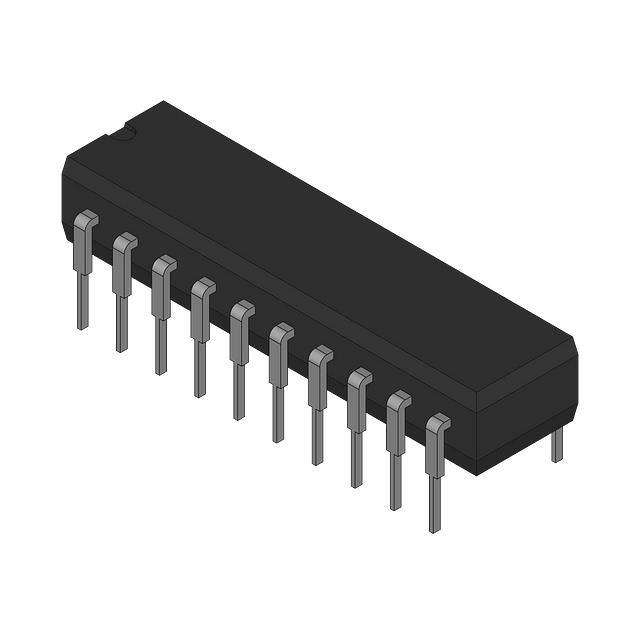


 工商网监
湘ICP备2023018690号
工商网监
湘ICP备2023018690号
