�������� �
���
� ������������� �� ����� ����������
SCLS609 − MARCH 2005
D Operates as a GTL-/GTL/GTL+ to LVTTL or
D
D
D
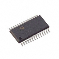
PW PACKAGE
(TOP VIEW)
LVTTL to GTL-/GTL/GTL+ Translator
Series Termination on TTL Outputs of 30��
Latch-Up Testing Done to JEDEC Standard
JESD 78
ESD Performance Tested Per JESD 22
− 2000-V Human-Body Model
(A114-B, Class II)
− 200-V Machine Model (A115-A)
− 1000-V Charged-Device Model (C101)
VREF
1AO
2AO
5A
6A
EN1
11BI
11A
9BI
3AO
4AO
10AI1
10AI2
GND
description/ordering information
The SN74GTL2007 is a 12-bit translator to
interface between the 3.3-V LVTTL chip set I/O
and the Xeon processor GTL-/GTL/GTL+ I/O.
The device is designed for platform health
management in dual-processor applications.
1
28
2
27
3
26
4
25
5
24
6
23
7
22
8
21
9
20
10
19
11
18
12
17
13
16
14
15
VCC
1BI
2BI
7BO1
7BO2
EN2
11BO
5BI
6BI
3BI
4BI
10BO1
10BO2
9AO
PIN DESCRIPTION
PIN NUMBER
SYMBOL
1
VREF
ENn
nAn
2-6, 8, 10-13,
15, 23
NAME AND FUNCTION
GTL reference voltage
Data and enable inputs/outputs (LVTTL)
7, 9, 16,
17−22, 24−27
nBn
Data inputs/outputs (GTL−/GTL/GTL+)
14
GND
Ground (0 V)
28
VCC
Positive supply voltage
ORDERING INFORMATION
−40°C to 85°C
ORDERABLE
PART NUMBER
PACKAGE†
TA
TSSOP − PW
Tube
SN74GTL2007PW
Tape and reel
SN74GTL2007PWR
TOP-SIDE
MARKING
GK2007
† Package drawings, standard packing quantities, thermal data, symbolization, and PCB design guidelines
are available at www.ti.com/sc/package.
Please be aware that an important notice concerning availability, standard warranty, and use in critical applications of
Texas Instruments semiconductor products and disclaimers thereto appears at the end of this data sheet.
All trademarks are the property of their respective owners.
Copyright 2005, Texas Instruments Incorporated
�������
�� ���� ����������� �! "#��$�� �! �� %#&'�"����� (��$)
���(#"�! "������ �� !%$"���"�����! %$� �*$ �$��! �� �$+�!
�!��#�$��!
!���(��( ,������-) ���(#"���� %��"$!!��. (�$! ��� �$"$!!���'- ��"'#($
�$!���. �� �'' %����$�$�!)
POST OFFICE BOX 655303
• DALLAS, TEXAS 75265
1
��������� �
���
� ������������� �� ����� ����������
SCLS609 − MARCH 2005
Function Tables
INPUTS
EN1
OUTPUT
1AO/2AO
1BI/2BI
H
L
L
H
H
H
L
X
H
EN2
3BI/4BI
OUTPUT
3AO/4AO
H
L
L
H
H
H
L
X
H
INPUTS
INPUT
9BI
OUTPUT
9AO
L
L
H
H
INPUTS
10AI1/10AI2
9BI
OUTPUT
10BO1/10BO2
L
L
L
L
H
L
H
L
L
H
H
H
INPUTS
EN2
5BI/6BI
INPUT/OUTPUT
5A/6A
(OPEN DRAIN)
OUTPUT
7BO1/7BO2
L
L‡
H†
H
L‡
H
H
L
H
H
H
L
L
L
H
L‡
H
L
H
L
H
H
H
H
L
INPUT
11BI
L
INPUT/OUTPUT
11A
(OPEN DRAIN)
L
L
H
OUTPUT
11BO
L
H
L‡
H
L
H
L
H
H = High voltage level
L = Low voltage level
† The enable on 7BO1/7BO2 includes a
delay that prevents a transient condition
(where 5BI/6BI goes from low to high, and
the low to high on 5A/6A lags up to 100 ns)
from causing a low glitch on the
7BO1/7BO2 outputs.
‡ Open-drain input/output terminal is driven
to a logic-low state by an external driver.
2
POST OFFICE BOX 655303
• DALLAS, TEXAS 75265
��������� �
���
� ������������� �� ����� ����������
SCLS609 − MARCH 2005
logic symbol
GTL2007
GTL V REF
1
1AO
2
27
26
LVTTL OUTPUTS
2AO
3
5A (OPEN DRAIN)
4
25
5
24
LVTTL INPUT EN1
6
23
GTL INPUT 11BI
7
22
LVTTL I/O 11A (OPEN DRAIN)
8
1BI
2BI
7BO1
GTL
OUTPUTS
LVTTL I/O
6A (OPEN DRAIN)
GTL INPUT 9BI
21
9
10
LVTTL OUTPUTS
18
11
17
10AI1
12
LVTTL INPUTS
16
10AI2
EN2 LVTTL INPUT
11BO GTL OUTPUT
5BI
DELAY1
19
4AO
7BO2
DELAY1
20
3AO
GTL
INPUTS
13
15
6BI
GTL
INPUTS
3BI
4BI
10BO1
GTL
OUTPUTS
10BO2
9AO LVTTL OUTPUT
NOTE A: The enable on 7BO1/7BO2 includes a delay that prevents a transient conditon (where 5BI/6BI go from low to high, and the low to high
on 5A/6A lags up to 100 ns) from causing a low glitch on the 7BO1/7BO2 outputs.
POST OFFICE BOX 655303
• DALLAS, TEXAS 75265
3
��������� �
���
� ������������� �� ����� ����������
SCLS609 − MARCH 2005
absolute maximum ratings over operating free-air temperature (unless otherwise noted)†‡
Supply voltage range, VCC . . . . . . . . . . . . . . . . . . . . . . . . . . . . . . . . . . . . . . . . . . . . . . . . . . . . . . . . . . . −0.5 to 4.6 V
Input voltage range, VI (see Note 2): A port (LVTTL) . . . . . . . . . . . . . . . . . . . . . . . . . . . . . . . . . . . . . −0.5 to 4.6 V
B port (GTL) . . . . . . . . . . . . . . . . . . . . . . . . . . . . . . . . . . . . . . . −0.5 to 4.6 V
Output voltage range, VO (output in OFF or HIGH state)(see Note 2): A port . . . . . . . . . . . . . . . . −0.5 to 4.6 V
B port . . . . . . . . . . . . . . . . −0.5 to 4.6 V
Input diode current, IIK (VI < 0) . . . . . . . . . . . . . . . . . . . . . . . . . . . . . . . . . . . . . . . . . . . . . . . . . . . . . . . . . . . −50 mA
Output diode current, IOK (VO < 0) . . . . . . . . . . . . . . . . . . . . . . . . . . . . . . . . . . . . . . . . . . . . . . . . . . . . . . . . −50 mA
Current into any output in the LOW state: A port . . . . . . . . . . . . . . . . . . . . . . . . . . . . . . . . . . . . . . . . . . . . . 32 mA
B port . . . . . . . . . . . . . . . . . . . . . . . . . . . . . . . . . . . . . . . . . . . . . 30 mA
Current into any output in the HIGH state, A port . . . . . . . . . . . . . . . . . . . . . . . . . . . . . . . . . . . . . . . . . . . . −32 mA
Package thermal impedance, θJA (see Note 1) . . . . . . . . . . . . . . . . . . . . . . . . . . . . . . . . . . . . . . . . . . . . . 62°C/W
Storage temperature range, Tstg . . . . . . . . . . . . . . . . . . . . . . . . . . . . . . . . . . . . . . . . . . . . . . . . . . . . . −60 to 150°C
† Stresses beyond those listed under “absolute maximum ratings” may cause permanent damage to the device. These are stress ratings only, and
functional operation of the device at these or any other conditions beyond those indicated under “recommended operating conditions” is not
implied. Exposure to absolute-maximum-rated conditions for extended periods may affect device reliability.
‡ Voltages are referenced to GND (ground = 0 V).
NOTES: 1. The performance capability of a high-performance integrated circuit, in conjunction with its thermal environment, can create junction
temperatures that are detrimental to reliability. The maximum junction temperature of this integrated circuit should not exceed 150°C.
2. The input and output negative voltage ratings may be exceeded if the input and output clamp current ratings are observed.
recommended operating conditions
VCC
VTT
VREF
MIN
NOM
MAX
3
3.3
3.6
GTL−
0.85
0.9
0.95
GTL
1.14
1.2
1.26
GTL+
1.35
1.5
1.65
Overall
0.5
2/3 VTT
1.8
GTL−
0.5
0.6
0.63
GTL
0.76
0.8
0.84
GTL+
0.87
1
1.1
A port
0
3.3
3.6
B port
0
VTT
3.6
Supply voltage
Termination voltage
Reference voltage
VI
Input voltage
VIH
HIGH-level input voltage
VIL
LOW-level input voltage
IOH
HIGH-level output current
IOL
LOW-level output current
TA
Operating free-air temperature range
A port
4
B port
V
V
V
V
2
V
VREF + 50 mV
A port
0.8
B port
VREF − 50 mV
−16
A port
A port
16
B port
15
POST OFFICE BOX 655303
UNIT
−40
• DALLAS, TEXAS 75265
85
V
mA
mA
°C
��������� �
���
� ������������� �� ����� ����������
SCLS609 − MARCH 2005
electrical characteristics over recommended operating conditions
PARAMETER
VOH‡
VOL‡
II
VCC = 3 V to 3.6 V, IOH = –100 mA
VCC = 3 V, IOH = –16 mA
A port
A port
B port
A port
B port
ICC
DICC§
CIO
–40�C TO +85�C
MIN
TYP†
MAX
TEST CONDITIONS
A or B port
A port or control inputs
VCC – 0.2
2.1
V
VCC = 3 V, IOL = 16 mA
VCC = 3 V, IOL = 15 mA
0.8
VCC = 3.6 V, VI = VCC
VCC = 3.6, VI = 0 V
±1
VCC = 3.6 V, VI = VTT or GND
VCC = 3.6 V, VI = VCC or GND, IO = 0
±1
0.4
±1
VCC = 3.6 V, VI = VCC – 0.6 V
VO = 3 V or 0
A port
VO = VTT or 0
† All typical values are measured at VCC = 3.3 V and TA = 25°C.
‡ The input and output voltage ratings may be exceeded if the input and output current ratings are observed.
§ This is the increase in supply current for each input that is at the specified LVTTL voltage, rather than VCC or GND.
V
mA
12
mA
500
mA
5
B port
UNIT
pF
4
switching characteristics over recommended operating free-air temperature range
GTL−
PARAMETER
WAVEFORM
tPLH
tPHL
An to Bn
1
tPLH
tPHL
Bn to An
2
tPLH
tPHL
9BI to 10BOn
3
tPLH
tPHL¶
11BI to 11BO
3
tPLH
tPHL
Bn to Bn
3
tPLH
tPHL
ENn to An
4
tPLZ
tPZL
Bn to An (I/O)
5
tPLZ
tPZL
EN2 to An (I/O)
6
GTL
VCC = 3.3 V � 0.3 V
VREF = 0.6 V
MIN TYP†
MAX
GTL+
VCC = 3.3 V � 0.3 V
VREF = 0.8 V
MIN TYP†
MAX
VCC = 3.3 V � 0.3 V
VREF = 1 V
MIN TYP†
MAX
2
4
8
2
4
8
2
4
8
2
5.5
10
2
5.5
10
2
5.5
10
2
5.5
10
2
5.5
10
2
5.5
10
2
5.5
10
2
5.5
10
2
5.5
10
2
6
11
2
6
11
2
6
11
2
6
11
2
6
11
2
6
11
2
8
13
2
8
13
2
8
13
2
14
21
2
14
21
2
14
21
4
7
11
4
7
11
4
7
11
120
205
350
120
205
350
120
205
350
1
3
7
1
3
7
1
3
7
1
3
7
1
3
7
1
3
7
2
5
10
2
5
10
2
5
10
2
5
10
2
5
10
2
5
10
1
3
7
1
3
7
1
3
7
1
3
7
1
3
7
1
3
7
UNIT
ns
ns
ns
ns
ns
ns
ns
ns
† All typical values are measured at VCC = 3.3 V and TA = 25°C.
¶ Includes ∼7.6-ns RC rise time of test-load pullup on 11-A, 1.5-kΩ pullup, and 21-pF load on 11 A has approximately 23-ns RC rise time.
POST OFFICE BOX 655303
• DALLAS, TEXAS 75265
5
��������� �
���
� ������������� �� ����� ����������
SCLS609 − MARCH 2005
PARAMETER MEASUREMENT INFORMATION
VTT = 1.2 V, VREF = 0.8 V FOR GTL AND VTT = 1.5 V, VREF = 1 V FOR GTL+
S1
500 Ω
From Output
Under Test
2 � VCC
VTT
Open
50 Ω
TEST
tPLH/tPHL
tPLZ/tPZL
GND
CL = 50 pF
(see Note A)
500 Ω
S1
Open
2 � VCC
From Output
Under Test
CL = 30 pF
(see Note A)
LOAD CIRCUIT FOR B OUTPUTS
LOAD CIRCUIT FOR A OUTPUTS
3V
Input
(see Note B)
1.5 V
Test
Point
1.5 V
Input
(see Note B)
VTT
VREF
VREF
0V
0V
tPHL
tPLH
tPHL
tPLH
VOH
VTT
Output
VREF
Output
VREF
1.5 V
1.5 V
VOL
VOL
VOLTAGE WAVEFORM 2
PROPAGATION DELAY TIMES
(B port to A port)†
VOLTAGE WAVEFORM 1
PROPAGATION DELAY TIMES
(A port to B port)†
Input
(see Note B)
VTT
VREF
VREF
Input
(see Note B)
3V
1.5 V
1.5 V
0V
0V
tPHL
tPLH
tPHL
tPLH
VOH
VTT
Output
VREF
Output
VREF
1.5 V
1.5 V
VOL
VOL
VOLTAGE WAVEFORM 3
PROPAGATION DELAY TIMES
(B port to B port)†
VOLTAGE WAVEFORM 4
PROPAGATION DELAY TIMES
(ENn to A port)†
VTT
Input
(see Note B)
VREF
VREF
3V
Input
(see Note B)
1.5 V
1.5 V
0V
0V
tPZL
Output
S1 at 2 � VCC
tPZL
tPLZ
VCC
1.5 V
Output
S1 at 2 � VCC
tPLZ
VCC
1.5 V
VOL + 0.3 V
VOL
VOLTAGE WAVEFORM 6
ENABLE AND DISABLE TIMES
(EN2 to A (I/O) port)†
VOL + 0.3 V
VOL
VOLTAGE WAVEFORM 5
PROPAGATION DELAY TIMES
(B port to A (I/O) port)†
† All control inputs are LVTTL levels.
NOTES: A. CL includes probe and jig capacitance.
B. All input pulses are supplied by generators having the following characteristics: PRR ≤ 10 MHz, ZO = 50 Ω, tr ≤ 2.5 ns, tf ≤ 2.5 ns.
C. The outputs are measured one at a time, with one transition per measurement.
Figure 1. Load Circuits and Voltage Waveforms
6
POST OFFICE BOX 655303
• DALLAS, TEXAS 75265
��������� �
���
� ������������� �� ����� ����������
SCLS609 − MARCH 2005
APPLICATION INFORMATION
VTT
VTT
56 �
56 �
R
VCC
1.5 k� to 1.2 k�
1.5 k�
2R
Platform
Health
Management
VCC
CPU1
VREF
VCC
CPU1 1ERR_L
1AO
1BI
1ERR_L
CPU1 THRMTRIP L
2AO
2BI
CPU1 PROCHOT L
5A
7BO1
THRMTRIP L
FORCEPR_L
CPU2 PROCHOT L
6A
7BO2
NMI_L
EN1
EN2
11BI
11B0
11A
5BI
6BI
3AO
CPU2 THRMTRIP L
4AO
CPU1 SMI L
CPU2 SMI L
NMI
CPU1 SMI L
9BI
CPU2 1ERR_L
PROCHOT L
FORCEPR_L
PROCHOT L
3BI
4BI
1ERR_L
THRMTRIP L
10AI1
10BO1
NMI
10AI2
10BO2
CPU2 SMI L
GND
9AO
CPU2
SMI_BUFF_L
GTL2007
Southbridge NMI
Southbridge SMI_L
PWR GD
Optional Signal Line
Power Supervisor
Frequently Asked Questions
Question 1: On the GTL2007 LVTTL input, specifically 10AI1 and 10AI2, when the GTL2007 is powered down,
these inputs may be pulled up to 3.3 V, and we want to ensure that there is no leakage path to the power rail
under this condition. Are the LVTTL inputs high impedance when the device is powered down, and will there
be any leakage?
Answer 1: When the device is powered down, the LVTTL inputs are in a high-impedance state and do not leak
to VDD if they are pulled high while the device is powered down.
Question 2: Do all the LVTTL inputs have the same powered-down characteristic?
Answer 2: Yes
Question 3: What is the condition of the other GTL I/O and LVTTL output pins when the device is powered
down?
Answer 3: The open-drain outputs, both GTL and LVTTL, do not leak to the power supply if they are pulled high
while the device is powered down. The GTL inputs also do not leak to the power supply under the same
conditions. The LVTTL totem-pole outputs, however, are not open-drain type outputs, and there is no current
flow on these pins if they are pulled high when VDD is at ground.
POST OFFICE BOX 655303
• DALLAS, TEXAS 75265
7
�PACKAGE OPTION ADDENDUM
www.ti.com
10-Dec-2020
PACKAGING INFORMATION
Orderable Device
Status
(1)
Package Type Package Pins Package
Drawing
Qty
Eco Plan
(2)
Lead finish/
Ball material
MSL Peak Temp
Op Temp (°C)
Device Marking
(3)
(4/5)
(6)
SN74GTL2007PW
ACTIVE
TSSOP
PW
28
50
RoHS & Green
NIPDAU
Level-1-260C-UNLIM
-40 to 85
GK2007
SN74GTL2007PWR
ACTIVE
TSSOP
PW
28
2000
RoHS & Green
NIPDAU
Level-1-260C-UNLIM
-40 to 85
GK2007
(1)
The marketing status values are defined as follows:
ACTIVE: Product device recommended for new designs.
LIFEBUY: TI has announced that the device will be discontinued, and a lifetime-buy period is in effect.
NRND: Not recommended for new designs. Device is in production to support existing customers, but TI does not recommend using this part in a new design.
PREVIEW: Device has been announced but is not in production. Samples may or may not be available.
OBSOLETE: TI has discontinued the production of the device.
(2)
RoHS: TI defines "RoHS" to mean semiconductor products that are compliant with the current EU RoHS requirements for all 10 RoHS substances, including the requirement that RoHS substance
do not exceed 0.1% by weight in homogeneous materials. Where designed to be soldered at high temperatures, "RoHS" products are suitable for use in specified lead-free processes. TI may
reference these types of products as "Pb-Free".
RoHS Exempt: TI defines "RoHS Exempt" to mean products that contain lead but are compliant with EU RoHS pursuant to a specific EU RoHS exemption.
Green: TI defines "Green" to mean the content of Chlorine (Cl) and Bromine (Br) based flame retardants meet JS709B low halogen requirements of


 工商网监
湘ICP备2023018690号
工商网监
湘ICP备2023018690号
