SN54HCT573, SN74HCT573
OCTAL TRANSPARENT D-TYPE LATCHES
WITH 3-STATE OUTPUTS
SCLS176E – MARCH 1984 – REVISED JULY 2003
D
D
D
D
D
D
SN54HCT573 . . . J OR W PACKAGE
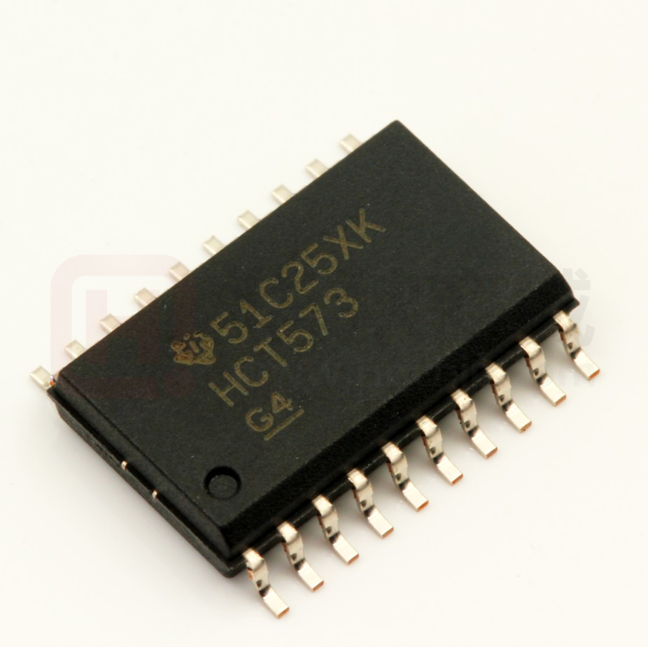
SN74HCT573 . . . DB, DW, N, NS, OR PW PACKAGE
(TOP VIEW)
Operating Voltage Range of 4.5 V to 5.5 V
High-Current 3-State Outputs Drive Bus
Lines Directly or Up To 15 LSTTL Loads
Low Power Consumption, 80-µA Max ICC
Typical tpd = 21 ns
±6-mA Output Drive at 5 V
Low Input Current of 1 µA Max
Inputs Are TTL-Voltage Compatible
Bus-Structured Pinout
OE
1D
2D
3D
4D
5D
6D
7D
8D
GND
description/ordering information
These octal transparent D-type latches feature
3-state outputs designed specifically for driving
highly capacitive or relatively low-impedance
loads. The ’HCT573 devices are particularly
suitable for implementing buffer registers, I/O
ports, bidirectional bus drivers, and working
registers.
1
20
2
19
3
18
4
17
5
16
6
15
7
14
8
13
9
12
10
11
VCC
1Q
2Q
3Q
4Q
5Q
6Q
7Q
8Q
LE
2D
1D
SN54HCT573 . . . FK PACKAGE
(TOP VIEW)
3D
4D
5D
6D
7D
While the latch-enable (LE) input is high, the
Q outputs respond to the data (D) inputs. When
LE is low, the outputs are latched to retain the data
that was set up at the D inputs.
OE
VCC
1Q
D
D
4
3 2 1 20 19
18
5
17
6
16
7
15
8
14
9 10 11 12 13
2Q
3Q
4Q
5Q
6Q
8D
GND
LE
8Q
7Q
A buffered output-enable (OE) input can be used
to place the eight outputs in either a normal logic
state (high or low logic levels) or the
high-impedance state. In the high-impedance
state, the outputs neither load nor drive the bus lines significantly. The high-impedance state and increased
drive provide the capability to drive bus lines without interface or pullup components.
ORDERING INFORMATION
PDIP – N
SN74HCT573N
Tube
SN74HCT573DW
Tape and reel
SN74HCT573DWR
SOP – NS
Tape and reel
SN74HCT573NSR
HCT573
SSOP – DB
Tape and reel
SN74HCT573DBR
HT573
Tube
SN74HCT573PW
Tape and reel
SN74HCT573PWR
CDIP – J
Tube
SNJ54HCT573J
SNJ54HCT573J
CFP – W
Tube
SNJ54HCT573W
SNJ54HCT573W
LCCC – FK
Tube
SNJ54HCT573FK
TSSOP – PW
–55°C to 125°C
TOP-SIDE
MARKING
Tube
SOIC – DW
–40°C to 85°C
ORDERABLE
PART NUMBER
PACKAGE†
TA
SN74HCT573N
HCT573
HT573
SNJ54HCT573FK
† Package drawings, standard packing quantities, thermal data, symbolization, and PCB design guidelines are
available at www.ti.com/sc/package.
Please be aware that an important notice concerning availability, standard warranty, and use in critical applications of
Texas Instruments semiconductor products and disclaimers thereto appears at the end of this data sheet.
Copyright 2003, Texas Instruments Incorporated
UNLESS OTHERWISE NOTED this document contains PRODUCTION
DATA information current as of publication date. Products conform to
specifications per the terms of Texas Instruments standard warranty.
Production processing does not necessarily include testing of all
parameters.
POST OFFICE BOX 655303
• DALLAS, TEXAS 75265
1
�SN54HCT573, SN74HCT573
OCTAL TRANSPARENT D-TYPE LATCHES
WITH 3-STATE OUTPUTS
SCLS176E – MARCH 1984 – REVISED JULY 2003
description/ordering information (continued)
OE does not affect the internal operations of the latches. Old data can be retained or new data can be entered
while the outputs are in the high-impedance state.
FUNCTION TABLE
(each latch)
INPUTS
OE
LE
D
OUTPUT
Q
L
H
H
H
L
H
L
L
L
L
X
Q0
H
X
X
Z
logic diagram (positive logic)
OE
LE
1
11
C1
1D
2
19
1Q
1D
To Seven Other Channels
absolute maximum ratings over operating free-air temperature range (unless otherwise noted)†
Supply voltage range, VCC . . . . . . . . . . . . . . . . . . . . . . . . . . . . . . . . . . . . . . . . . . . . . . . . . . . . . . . . . . –0.5 V to 7 V
Input clamp current, IIK (VI < 0 or VI > VCC) (see Note 1) . . . . . . . . . . . . . . . . . . . . . . . . . . . . . . . . . . . . ±20 mA
Output clamp current, IOK (VO < 0 or VO > VCC) (see Note 1) . . . . . . . . . . . . . . . . . . . . . . . . . . . . . . . . ±20 mA
Continuous output current, IO (VO = 0 to VCC) . . . . . . . . . . . . . . . . . . . . . . . . . . . . . . . . . . . . . . . . . . . . . . ±35 mA
Continuous current through VCC or GND . . . . . . . . . . . . . . . . . . . . . . . . . . . . . . . . . . . . . . . . . . . . . . . . . . . ±70 mA
Package thermal impedance, θJA (see Note 2): DB package . . . . . . . . . . . . . . . . . . . . . . . . . . . . . . . . . 70°C/W
DW package . . . . . . . . . . . . . . . . . . . . . . . . . . . . . . . . . 58°C/W
N package . . . . . . . . . . . . . . . . . . . . . . . . . . . . . . . . . . . 69°C/W
NS package . . . . . . . . . . . . . . . . . . . . . . . . . . . . . . . . . 60°C/W
PW package . . . . . . . . . . . . . . . . . . . . . . . . . . . . . . . . . 83°C/W
Storage temperature range, Tstg . . . . . . . . . . . . . . . . . . . . . . . . . . . . . . . . . . . . . . . . . . . . . . . . . . . –65°C to 150°C
† Stresses beyond those listed under “absolute maximum ratings” may cause permanent damage to the device. These are stress ratings only, and
functional operation of the device at these or any other conditions beyond those indicated under “recommended operating conditions” is not
implied. Exposure to absolute-maximum-rated conditions for extended periods may affect device reliability.
NOTES: 1. The input and output voltage ratings may be exceeded if the input and output current ratings are observed.
2. The package thermal impedance is calculated in accordance with JESD 51-7.
2
POST OFFICE BOX 655303
• DALLAS, TEXAS 75265
�SN54HCT573, SN74HCT573
OCTAL TRANSPARENT D-TYPE LATCHES
WITH 3-STATE OUTPUTS
SCLS176E – MARCH 1984 – REVISED JULY 2003
recommended operating conditions (see Note 3)
SN54HCT573
NOM
MAX
MIN
NOM
MAX
4.5
5
5.5
4.5
5
5.5
VCC
VIH
Supply voltage
VIL
VI
Low-level input voltage
Input voltage
0
VO
∆t/∆v
Output voltage
0
High-level input voltage
SN74HCT573
MIN
VCC = 4.5 V to 5.5 V
VCC = 4.5 V to 5.5 V
2
2
Input transition rise/fall time
V
V
0.8
VCC
VCC
UNIT
0
0
500
0.8
V
VCC
VCC
V
500
ns
V
TA
Operating free-air temperature
–55
125
–40
85
°C
NOTE 3: All unused inputs of the device must be held at VCC or GND to ensure proper device operation. Refer to the TI application report,
Implications of Slow or Floating CMOS Inputs, literature number SCBA004.
electrical characteristics over recommended operating free-air temperature range (unless
otherwise noted)
PARAMETER
TEST CONDITIONS
VCC
VOH
VI = VIH or VIL
IOH = –20 µA
IOH = –6 mA
45V
4.5
VOL
VI = VIH or VIL
IOL = 20 µA
IOL = 6 mA
45V
4.5
II
IOZ
VI = VCC or 0
VO = VCC or 0
ICC
VI = VCC or 0,
IO = 0
One input at 0.5 V or 2.4 V,
Other inputs at 0 or VCC
5.5 V
∆ICC†
MIN
SN54HCT573
MIN
MAX
SN74HCT573
MIN
4.4
4.499
4.4
4.4
3.98
4.3
3.7
3.84
MAX
UNIT
V
0.001
0.1
0.1
0.1
0.17
0.26
0.4
0.33
5.5 V
±0.1
±100
±1000
±1000
nA
5.5 V
±0.01
±0.5
±10
±5
µA
8
160
80
µA
1.4
2.4
3
2.9
mA
3
10
10
10
pF
5.5 V
4.5 V
to 5.5 V
Ci
TA = 25°C
TYP
MAX
V
† This is the increase in supply current for each input that is at one of the specified TTL voltage levels, rather than 0 V or VCC.
timing requirements over recommended operating free-air temperature range (unless otherwise
noted)
VCC
tw
Pulse duration,
duration LE high
tsu
Setup time,
time data before LE↓
th
Hold time,
time data after LE↓
TA = 25°C
MIN
MAX
SN54HCT573
MIN
MAX
SN74HCT573
MIN
4.5 V
20
30
25
5.5 V
17
27
23
4.5 V
10
15
13
5.5 V
9
14
12
4.5 V
5
5
5
5.5 V
5
5
5
MAX
UNIT
ns
ns
ns
PRODUCT PREVIEW information concerns products in the formative or
design phase of development. Characteristic data and other
specifications are design goals. Texas Instruments reserves the right to
change or discontinue these products without notice.
POST OFFICE BOX 655303
• DALLAS, TEXAS 75265
3
�SN54HCT573, SN74HCT573
OCTAL TRANSPARENT D-TYPE LATCHES
WITH 3-STATE OUTPUTS
SCLS176E – MARCH 1984 – REVISED JULY 2003
switching characteristics over recommended operating free-air temperature range, CL = 50 pF
(unless otherwise noted) (see Figure 1)
PARAMETER
FROM
(INPUT)
TO
(OUTPUT)
D
Q
tpd
d
LE
Any Q
ten
OE
Any Q
tdis
di
OE
Any Q
tt
Any Q
VCC
MIN
TA = 25°C
TYP
MAX
SN54HCT573
MIN
MAX
SN74HCT573
MIN
MAX
4.5 V
25
35
53
44
5.5 V
21
32
48
40
4.5 V
28
35
53
44
5.5 V
25
32
48
40
4.5 V
26
35
53
44
5.5 V
23
32
48
40
4.5 V
23
35
53
44
5.5 V
22
32
48
40
4.5 V
9
12
18
15
5.5 V
9
11
16
14
UNIT
ns
ns
ns
ns
switching characteristics over recommended operating free-air temperature range, CL = 150 pF
(unless otherwise noted) (see Figure 1)
PARAMETER
FROM
(INPUT)
TO
(OUTPUT)
D
Q
tpd
d
ten
tt
LE
Any Q
OE
Any Q
Any Q
VCC
MIN
TA = 25°C
TYP
MAX
SN54HCT573
MIN
MAX
SN74HCT573
MIN
MAX
4.5 V
32
52
79
65
5.5 V
27
47
71
59
4.5 V
38
52
79
65
5.5 V
36
47
71
59
4.5 V
33
52
79
65
5.5 V
28
47
71
59
4.5 V
18
42
63
53
5.5 V
16
38
57
48
UNIT
ns
ns
ns
operating characteristics, TA = 25°C
PARAMETER
Cpd
TEST CONDITIONS
Power dissipation capacitance per latch
No load
PRODUCT PREVIEW information concerns products in the formative or
design phase of development. Characteristic data and other
specifications are design goals. Texas Instruments reserves the right to
change or discontinue these products without notice.
4
POST OFFICE BOX 655303
• DALLAS, TEXAS 75265
TYP
50
UNIT
pF
�SN54HCT573, SN74HCT573
OCTAL TRANSPARENT D-TYPE LATCHES
WITH 3-STATE OUTPUTS
SCLS176E – MARCH 1984 – REVISED JULY 2003
PARAMETER MEASUREMENT INFORMATION
VCC
S1
Test
Point
From Output
Under Test
PARAMETER
ten
RL
tdis
CL
(see Note A)
S2
tPZH
RL
1 kΩ
tPZL
tPHZ
tPLZ
tpd or tt
1 kΩ
CL
S1
S2
50 pF
or
150 pF
Open
Closed
Closed
Open
Open
Closed
Closed
Open
Open
Open
50 pF
50 pF
or
150 pF
––
LOAD CIRCUIT
3V
High-Level
Pulse
1.3 V
3V
Reference
Input
1.3 V
0V
1.3 V
tsu
0V
tw
Data
Input 1.3 V
0.3 V
3V
Low-Level
Pulse
1.3 V
1.3 V
Output
Control
(Low-Level
Enabling)
3V
1.3 V
0V
tPLH
In-Phase
Output
1.3 V
10%
tPHL
90%
90%
tr
Out-ofPhase
Output
tPHL
90%
VOH
1.3 V
10% V
OL
tf
1.3 V
10%
tf
3V
1.3 V
0.3 V 0 V
tf
3V
1.3 V
1.3 V
0V
tPZL
Output
Waveform 1
(See Note B)
tPLZ
≈VCC
1.3 V
10%
tPZH
tPLH
1.3 V
10%
2.7 V
VOLTAGE WAVEFORMS
SETUP AND HOLD AND INPUT RISE AND FALL TIMES
VOLTAGE WAVEFORMS
PULSE DURATIONS
1.3 V
2.7 V
tr
0V
Input
th
90%
VOH
VOL
tr
VOLTAGE WAVEFORMS
PROPAGATION DELAY AND OUTPUT RISE AND FALL TIMES
Output
Waveform 2
(See Note B)
VOL
tPHZ
1.3 V
90%
VOH
≈0 V
VOLTAGE WAVEFORMS
ENABLE AND DISABLE TIMES FOR 3-STATE OUTPUTS
NOTES: A. CL includes probe and test-fixture capacitance.
B. Waveform 1 is for an output with internal conditions such that the output is low except when disabled by the output control.
Waveform 2 is for an output with internal conditions such that the output is high except when disabled by the output control.
C. Phase relationships between waveforms were chosen arbitrarily. All input pulses are supplied by generators having the following
characteristics: PRR ≤ 1 MHz, ZO = 50 Ω, tr = 6 ns, tf = 6 ns.
D. The outputs are measured one at a time with one input transition per measurement.
E. tPLZ and tPHZ are the same as tdis.
F. tPZL and tPZH are the same as ten.
G. tPLH and tPHL are the same as tpd.
Figure 1. Load Circuit and Voltage Waveforms
POST OFFICE BOX 655303
• DALLAS, TEXAS 75265
5
�PACKAGE OPTION ADDENDUM
www.ti.com
24-Aug-2018
PACKAGING INFORMATION
Orderable Device
Status
(1)
Package Type Package Pins Package
Drawing
Qty
Eco Plan
Lead/Ball Finish
MSL Peak Temp
(2)
(6)
(3)
Op Temp (°C)
Device Marking
(4/5)
SN74HCT573DBR
ACTIVE
SSOP
DB
20
2000
Green (RoHS
& no Sb/Br)
CU NIPDAU
Level-1-260C-UNLIM
-40 to 85
HT573
SN74HCT573DBRG4
ACTIVE
SSOP
DB
20
2000
Green (RoHS
& no Sb/Br)
CU NIPDAU
Level-1-260C-UNLIM
-40 to 85
HT573
SN74HCT573DW
ACTIVE
SOIC
DW
20
25
Green (RoHS
& no Sb/Br)
CU NIPDAU
Level-1-260C-UNLIM
-40 to 85
HCT573
SN74HCT573DWG4
ACTIVE
SOIC
DW
20
25
Green (RoHS
& no Sb/Br)
CU NIPDAU
Level-1-260C-UNLIM
-40 to 85
HCT573
SN74HCT573DWR
ACTIVE
SOIC
DW
20
2000
Green (RoHS
& no Sb/Br)
CU NIPDAU
Level-1-260C-UNLIM
-40 to 85
HCT573
SN74HCT573DWRE4
ACTIVE
SOIC
DW
20
2000
Green (RoHS
& no Sb/Br)
CU NIPDAU
Level-1-260C-UNLIM
-40 to 85
HCT573
SN74HCT573DWRG4
ACTIVE
SOIC
DW
20
2000
Green (RoHS
& no Sb/Br)
CU NIPDAU
Level-1-260C-UNLIM
-40 to 85
HCT573
SN74HCT573N
ACTIVE
PDIP
N
20
20
Pb-Free
(RoHS)
CU NIPDAU
N / A for Pkg Type
-40 to 85
SN74HCT573N
SN74HCT573NSR
ACTIVE
SO
NS
20
2000
Green (RoHS
& no Sb/Br)
CU NIPDAU
Level-1-260C-UNLIM
-40 to 85
HCT573
SN74HCT573PW
ACTIVE
TSSOP
PW
20
70
Green (RoHS
& no Sb/Br)
CU NIPDAU
Level-1-260C-UNLIM
-40 to 85
HT573
SN74HCT573PWR
ACTIVE
TSSOP
PW
20
2000
Green (RoHS
& no Sb/Br)
CU NIPDAU
Level-1-260C-UNLIM
-40 to 85
HT573
(1)
The marketing status values are defined as follows:
ACTIVE: Product device recommended for new designs.
LIFEBUY: TI has announced that the device will be discontinued, and a lifetime-buy period is in effect.
NRND: Not recommended for new designs. Device is in production to support existing customers, but TI does not recommend using this part in a new design.
PREVIEW: Device has been announced but is not in production. Samples may or may not be available.
OBSOLETE: TI has discontinued the production of the device.
(2)
RoHS: TI defines "RoHS" to mean semiconductor products that are compliant with the current EU RoHS requirements for all 10 RoHS substances, including the requirement that RoHS substance
do not exceed 0.1% by weight in homogeneous materials. Where designed to be soldered at high temperatures, "RoHS" products are suitable for use in specified lead-free processes. TI may
reference these types of products as "Pb-Free".
RoHS Exempt: TI defines "RoHS Exempt" to mean products that contain lead but are compliant with EU RoHS pursuant to a specific EU RoHS exemption.
Green: TI defines "Green" to mean the content of Chlorine (Cl) and Bromine (Br) based flame retardants meet JS709B low halogen requirements of


 工商网监
湘ICP备2023018690号
工商网监
湘ICP备2023018690号
