SN54LV139A, SN74LV139A
DUAL 2-LINE TO 4-LINE DECODERS/DEMULTIPLEXERS
SCLS396I − APRIL 1998 − REVISED APRIL 2005
D 2-V to 5.5-V VCC Operation
D Max tpd of 7.5 ns at 5 V
D Support Mixed-Mode Voltage Operation on
D
All Ports
Designed Specifically for High-Speed
Memory Decoders and Data-Transmission
Systems
Incorporate Two Enable Inputs to Simplify
Cascading and/or Data Reception
SN54LV139A . . . J OR W PACKAGE
SN74LV139A . . . D, DB, DGV, NS,
OR PW PACKAGE
(TOP VIEW)
15
3
14
4
13
5
12
6
11
7
10
8
9
VCC
2G
2A
2B
2Y0
2Y1
2Y2
2Y3
1A
1B
1Y0
1Y1
1Y2
1Y3
16
1A
1G
NC
VCC
2G
1
2
15
3
14
4
13
5
12
6
11
10
7
8
9
1B
1Y0
NC
1Y1
1Y2
2G
2A
2B
2Y0
2Y1
2Y2
4
3 2 1 20 19
18
5
17
6
16
7
15
8
14
9 10 11 12 13
2A
2B
NC
2Y0
2Y1
1Y3
GND
NC
2Y3
2Y2
16
2
VCC
1
SN54LV139A . . . FK PACKAGE
(TOP VIEW)
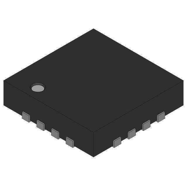
SN74LV139A . . . RGY PACKAGE
(TOP VIEW)
2Y3
1G
1A
1B
1Y0
1Y1
1Y2
1Y3
GND
D
1G
D
Operation
Latch-Up Performance Exceeds 250 mA Per
JESD 17
ESD Protection Exceeds JESD 22
− 2000-V Human-Body Model (A114-A)
− 200-V Machine Model (A115-A)
− 1000-V Charged-Device Model (C101)
GND
D
D Ioff Supports Partial-Power-Down Mode
NC − No internal connection
description/ordering information
The ’LV139A devices are dual 2-line to 4-line decoders/demultiplexers designed for 2-V to 5.5-V VCC operation.
ORDERING INFORMATION
QFN − RGY
SN74LV139ARGYR
Tube of 40
SN74LV139AD
Reel of 2500
SN74LV139ADR
SOP − NS
Reel of 2000
SN74LV139ANSR
74LV139A
SSOP − DB
Reel of 2000
SN74LV139ADBR
LV139A
Tube of 90
SN74LV139APW
Reel of 2000
SN74LV139APWR
Reel of 250
SN74LV139APWT
TVSOP − DGV
Reel of 2000
SN74LV139ADGVR
LV139A
CDIP − J
Tube of 25
SNJ54LV139AJ
SNJ54LV139AJ
CFP − W
Tube of 150
SNJ54LV139AW
SNJ54LV139AW
LCCC − FK
Tube of 55
SNJ54LV139AFK
SNJ54LV139AFK
TSSOP − PW
−55°C to 125°C
†
TOP-SIDE
MARKING
Reel of 1000
SOIC − D
−40°C
40 C to 85°C
85 C
ORDERABLE
PART NUMBER
PACKAGE†
TA
LV139A
LV139A
LV139A
Package drawings, standard packing quantities, thermal data, symbolization, and PCB design
guidelines are available at www.ti.com/sc/package.
Please be aware that an important notice concerning availability, standard warranty, and use in critical applications of
Texas Instruments semiconductor products and disclaimers thereto appears at the end of this data sheet.
Copyright © 2005, Texas Instruments Incorporated
UNLESS OTHERWISE NOTED this document contains PRODUCTION
DATA information current as of publication date. Products conform to
specifications per the terms of Texas Instruments standard warranty.
Production processing does not necessarily include testing of all
parameters.
POST OFFICE BOX 655303
• DALLAS, TEXAS 75265
1
�SN54LV139A, SN74LV139A
DUAL 2-LINE TO 4-LINE DECODERS/DEMULTIPLEXERS
SCLS396I − APRIL 1998 − REVISED APRIL 2005
description/ordering information (continued)
These devices are designed for high-performance memory-decoding or data-routing applications requiring very
short propagation delay times. In high-performance memory systems, these decoders can minimize the effects
of system decoding. When employed with high-speed memories utilizing a fast enable circuit, the delay time
of these decoders and the enable time of the memory usually are less than the typical access time of the
memory. This means that the effective system delay introduced by the decoders is negligible.
The ’LV139A devices comprise two individual 2-line to 4-line decoders in a single package. The active-low
enable (G) input can be used as a data line in demultiplexing applications. These decoders/demultiplexers
feature fully buffered inputs, each of which represents only one normalized load to its driving circuit.
These devices are fully specified for partial-power-down applications using Ioff. The Ioff circuitry disables the
outputs, preventing damaging current backflow through the devices when they are powered down.
FUNCTION TABLE
INPUTS
OUTPUTS
SELECT
G
2
B
A
Y0
Y1
Y2
Y3
H
X
X
H
H
H
H
L
L
L
L
H
H
H
L
L
H
H
L
H
H
L
H
L
H
H
L
H
L
H
H
H
H
H
L
POST OFFICE BOX 655303
• DALLAS, TEXAS 75265
�SN54LV139A, SN74LV139A
DUAL 2-LINE TO 4-LINE DECODERS/DEMULTIPLEXERS
SCLS396I − APRIL 1998 − REVISED APRIL 2005
logic diagram (positive logic)
4
1G
1
1Y0
5
1Y1
6
1Y2
2
1A
7
1B
1Y3
3
12
2Y0
15
11
2G
2Y1
10
2Y2
2A
14
9
13
2Y3
2B
Pin numbers shown are for the D, DB, DGV, J, NS, PW, RGY, and W packages.
absolute maximum ratings over operating free-air temperature range (unless otherwise noted)†
Supply voltage range, VCC . . . . . . . . . . . . . . . . . . . . . . . . . . . . . . . . . . . . . . . . . . . . . . . . . . . . . . . . . . −0.5 V to 7 V
Input voltage range, VI (see Note 1) . . . . . . . . . . . . . . . . . . . . . . . . . . . . . . . . . . . . . . . . . . . . . . . . . . −0.5 V to 7 V
Voltage range applied to any output in the high-impedance
or power-off state, VO (see Note 1) . . . . . . . . . . . . . . . . . . . . . . . . . . . . . . . . . . . . . . . . . . . . . . . . . −0.5 V to 7 V
Output voltage range, VO (see Notes 1 and 2) . . . . . . . . . . . . . . . . . . . . . . . . . . . . . . . . . . −0.5 V to VCC + 0.5 V
Input clamp current, IIK (VI < 0) . . . . . . . . . . . . . . . . . . . . . . . . . . . . . . . . . . . . . . . . . . . . . . . . . . . . . . . . . . . −20 mA
Output clamp current, IOK (VO < 0) . . . . . . . . . . . . . . . . . . . . . . . . . . . . . . . . . . . . . . . . . . . . . . . . . . . . . . . . −50 mA
Continuous output current, IO (VO = 0 to VCC) . . . . . . . . . . . . . . . . . . . . . . . . . . . . . . . . . . . . . . . . . . . . . . ±25 mA
Continuous current through VCC or GND . . . . . . . . . . . . . . . . . . . . . . . . . . . . . . . . . . . . . . . . . . . . . . . . . . . ±50 mA
Package thermal impedance, θJA (see Note 3): D package . . . . . . . . . . . . . . . . . . . . . . . . . . . . . . . . . . . 73°C/W
(see Note 3): DB package . . . . . . . . . . . . . . . . . . . . . . . . . . . . . . . . . 82°C/W
(see Note 3): DGV package . . . . . . . . . . . . . . . . . . . . . . . . . . . . . . . 120°C/W
(see Note 3): NS package . . . . . . . . . . . . . . . . . . . . . . . . . . . . . . . . . 64°C/W
(see Note 3): PW package . . . . . . . . . . . . . . . . . . . . . . . . . . . . . . . . 108°C/W
(see Note 4): RGY package . . . . . . . . . . . . . . . . . . . . . . . . . . . . . . . . 39°C/W
Storage temperature range, Tstg . . . . . . . . . . . . . . . . . . . . . . . . . . . . . . . . . . . . . . . . . . . . . . . . . . . −65°C to 150°C
†
Stresses beyond those listed under “absolute maximum ratings” may cause permanent damage to the device. These are stress ratings only, and
functional operation of the device at these or any other conditions beyond those indicated under “recommended operating conditions” is not
implied. Exposure to absolute-maximum-rated conditions for extended periods may affect device reliability.
NOTES: 1. The input and output negative-voltage ratings may be exceeded if the input and output current ratings are observed.
2. This value is limited to 5.5 V maximum.
3. The package thermal impedance is calculated in accordance with JESD 51-7.
4. The package thermal impedance is calculated in accordance with JESD 51-5.
POST OFFICE BOX 655303
• DALLAS, TEXAS 75265
3
�SN54LV139A, SN74LV139A
DUAL 2-LINE TO 4-LINE DECODERS/DEMULTIPLEXERS
SCLS396I − APRIL 1998 − REVISED APRIL 2005
recommended operating conditions (see Note 5)
SN54LV139A
VCC
MIN
MAX
2
5.5
Supply voltage
VCC = 2 V
VIH
High level input voltage
High-level
1.5
Low level input voltage
Low-level
VI
Input voltage
VO
Output voltage
VCC × 0.7
VCC × 0.7
VCC × 0.7
VCC = 4.5 V to 5.5 V
VCC × 0.7
VCC × 0.7
Input transition rise or fall rate
TA
Operating free-air temperature
V
V
0.5
0.5
VCC × 0.3
VCC × 0.3
VCC = 3 V to 3.6 V
VCC × 0.3
VCC × 0.3
VCC × 0.3
5.5
0
5.5
0
VCC
0
VCC = 3 V to 3.6 V
VCC
V
−50
μA
−2
−2
−6
−6
−12
50
50
VCC = 2.3 V to 2.7 V
2
2
VCC = 3 V to 3.6 V
6
6
VCC = 4.5 V to 5.5 V
12
12
VCC = 2.3 V to 2.7 V
200
200
VCC = 3 V to 3.6 V
100
100
20
−55
V
−50
−12
VCC = 4.5 V to 5.5 V
V
VCC × 0.3
0
VCC = 2 V
Δt/Δv
UNIT
VCC = 2.3 V to 2.7 V
VCC = 2.3 V to 2.7 V
Low level output current
Low-level
5.5
VCC × 0.7
VCC = 4.5 V to 5.5 V
IOL
2
VCC = 2.3 V to 2.7 V
VCC = 2 V
High level output current
High-level
MAX
VCC = 3 V to 3.6 V
VCC = 4.5 V to 5.5 V
IOH
MIN
1.5
VCC = 2 V
VIL
SN74LV139A
125
mA
μA
mA
ns/V
20
−40
°C
85
NOTE 5: All unused inputs of the device must be held at VCC or GND to ensure proper device operation. Refer to the TI application report,
Implications of Slow or Floating CMOS Inputs, literature number SCBA004.
electrical characteristics over recommended operating free-air temperature range (unless
otherwise noted)
SN54LV139A
PARAMETER
VOH
TEST CONDITIONS
MIN
TYP
MIN
2 V to 5.5 V
IOH = −2 mA
2.3 V
2
2
IOH = −6 mA
3V
2.48
2.48
4.5 V
3.8
VCC−0.1
TYP
MAX
V
3.8
2 V to 5.5 V
0.1
0.1
IOL = 2 mA
2.3 V
0.4
0.4
IOL = 6 mA
3V
0.44
0.44
4.5 V
II
VI = 5.5 V or GND
ICC
VI = VCC or GND,
Ioff
VI or VO = 0 to 5.5 V
Ci
VI = VCC or GND
IO = 0
UNIT
VCC−0.1
IOL = 50 μA
IOL = 12 mA
V
0.55
0.55
0 to 5.5 V
±1
±1
μA
5.5 V
20
20
μA
0
5
5
μA
3.3 V
1.9
PRODUCT PREVIEW information concerns products in the formative or
design phase of development. Characteristic data and other
specifications are design goals. Texas Instruments reserves the right to
change or discontinue these products without notice.
4
SN74LV139A
MAX
IOH = −50 μA
IOH = −12 mA
VOL
VCC
POST OFFICE BOX 655303
• DALLAS, TEXAS 75265
1.9
pF
�SN54LV139A, SN74LV139A
DUAL 2-LINE TO 4-LINE DECODERS/DEMULTIPLEXERS
SCLS396I − APRIL 1998 − REVISED APRIL 2005
switching characteristics over recommended operating
VCC = 2.5 V ± 0.2 V (unless otherwise noted) (see Figure 1)
PARAMETER
tpd
tpd
FROM
(INPUT)
TO
(OUTPUT)
A or B
Y
G
Y
A or B
Y
G
Y
LOAD
CAPACITANCE
free-air
TA = 25°C
MIN
CL = 15 pF
CL = 50 pF
temperature
SN54LV139A
range,
SN74LV139A
TYP
MAX
MIN
MAX
MIN
MAX
7.7*
17.6*
1*
21*
1
21
7.4*
15.8*
1*
19*
1
19
10.2
22.5
1
26.5
1
26.5
9.9
20.2
1
24
1
24
UNIT
ns
ns
* On products compliant to MIL-PRF-38535, this parameter is not production tested.
switching characteristics over recommended operating
VCC = 3.3 V ± 0.3 V (unless otherwise noted) (see Figure 1)
PARAMETER
tpd
tpd
FROM
(INPUT)
TO
(OUTPUT)
A or B
Y
G
Y
A or B
Y
G
Y
LOAD
CAPACITANCE
free-air
TA = 25°C
MIN
TYP
CL = 15 pF
CL = 50 pF
temperature
SN54LV139A
range,
SN74LV139A
MAX
MIN
MAX
MIN
MAX
5.3*
11*
1*
13*
1
13
5.1*
9.2*
1*
11*
1
11
7.3
14.5
1
16.5
1
16.5
7
12.7
1
14.5
1
14.5
UNIT
ns
ns
* On products compliant to MIL-PRF-38535, this parameter is not production tested.
switching characteristics over recommended operating
VCC = 5 V ± 0.5 V (unless otherwise noted) (see Figure 1)
PARAMETER
tpd
tpd
FROM
(INPUT)
TO
(OUTPUT)
A or B
Y
G
Y
A or B
Y
G
Y
LOAD
CAPACITANCE
free-air
TA = 25°C
MIN
CL = 15 pF
CL = 50 pF
temperature
SN54LV139A
range,
SN74LV139A
TYP
MAX
MIN
MAX
MIN
MAX
3.7*
7.2*
1*
8.5*
1
8.5
3.5*
6.3*
1*
7.5*
1
7.5
5.2
9.2
1
10.5
1
10.5
4.9
8.3
1
9.5
1
9.5
UNIT
ns
ns
* On products compliant to MIL-PRF-38535, this parameter is not production tested.
operating characteristics, TA = 25°C
PARAMETER
Cpd
Power dissipation capacitance
TEST CONDITIONS
pF
CL = 50 pF,
f = 10 MHz
VCC
TYP
3.3 V
17.3
5V
18.2
UNIT
pF
PRODUCT PREVIEW information concerns products in the formative or
design phase of development. Characteristic data and other
specifications are design goals. Texas Instruments reserves the right to
change or discontinue these products without notice.
POST OFFICE BOX 655303
• DALLAS, TEXAS 75265
5
�SN54LV139A, SN74LV139A
DUAL 2-LINE TO 4-LINE DECODERS/DEMULTIPLEXERS
SCLS396I − APRIL 1998 − REVISED APRIL 2005
PARAMETER MEASUREMENT INFORMATION
VCC
From Output
Under Test
Test
Point
RL = 1 kΩ
From Output
Under Test
CL
(see Note A)
S1
Open
TEST
GND
S1
tPLH/tPHL
tPLZ/tPZL
tPHZ/tPZH
Open Drain
CL
(see Note A)
Open
VCC
GND
VCC
LOAD CIRCUIT FOR
3-STATE AND OPEN-DRAIN OUTPUTS
LOAD CIRCUIT FOR
TOTEM-POLE OUTPUTS
VCC
50% VCC
Timing Input
0V
tw
tsu
VCC
50% VCC
50% VCC
Input
th
VCC
50% VCC
Data Input
50% VCC
0V
0V
VOLTAGE WAVEFORMS
PULSE DURATION
VOLTAGE WAVEFORMS
SETUP AND HOLD TIMES
VCC
50% VCC
Input
50% VCC
tPLH
tPHL
50% VCC
tPHL
50% VCC
VOL
tPLZ
≈VCC
50% VCC
tPZH
VOH
50% VCC
VOL
Output
Waveform 2
S1 at GND
(see Note B)
VOLTAGE WAVEFORMS
PROPAGATION DELAY TIMES
INVERTING AND NONINVERTING OUTPUTS
50% VCC
0V
Output
Waveform 1
S1 at VCC
(see Note B)
tPLH
50% VCC
50% VCC
tPZL
VOH
In-Phase
Output
Out-of-Phase
Output
0V
VC C
Output
Control
VOL + 0.3 V
VOL
tPHZ
50% VCC
VOH − 0.3 V
VOH
≈0 V
VOLTAGE WAVEFORMS
ENABLE AND DISABLE TIMES
LOW- AND HIGH-LEVEL ENABLING
NOTES: A. CL includes probe and jig capacitance.
B. Waveform 1 is for an output with internal conditions such that the output is low, except when disabled by the output control.
Waveform 2 is for an output with internal conditions such that the output is high, except when disabled by the output control.
C. All input pulses are supplied by generators having the following characteristics: PRR ≤ 1 MHz, ZO = 50 Ω, tr ≤ 3 ns, tf ≤ 3 ns.
D. The outputs are measured one at a time, with one input transition per measurement.
E. tPLZ and tPHZ are the same as tdis.
F. tPZL and tPZH are the same as ten.
G. tPHL and tPLH are the same as tpd.
H. All parameters and waveforms are not applicable to all devices.
Figure 1. Load Circuit and Voltage Waveforms
6
POST OFFICE BOX 655303
• DALLAS, TEXAS 75265
�PACKAGE OPTION ADDENDUM
www.ti.com
13-Aug-2021
PACKAGING INFORMATION
Orderable Device
Status
(1)
Package Type Package Pins Package
Drawing
Qty
Eco Plan
(2)
Lead finish/
Ball material
MSL Peak Temp
Op Temp (°C)
Device Marking
(3)
(4/5)
(6)
SN74LV139AD
ACTIVE
SOIC
D
16
40
RoHS & Green
NIPDAU
Level-1-260C-UNLIM
-40 to 85
LV139A
SN74LV139ADBR
ACTIVE
SSOP
DB
16
2000
RoHS & Green
NIPDAU
Level-1-260C-UNLIM
-40 to 85
LV139A
SN74LV139ADR
ACTIVE
SOIC
D
16
2500
RoHS & Green
NIPDAU
Level-1-260C-UNLIM
-40 to 85
LV139A
SN74LV139ANSR
ACTIVE
SO
NS
16
2000
RoHS & Green
NIPDAU
Level-1-260C-UNLIM
-40 to 85
74LV139A
SN74LV139ANSRE4
ACTIVE
SO
NS
16
2000
RoHS & Green
NIPDAU
Level-1-260C-UNLIM
-40 to 85
74LV139A
SN74LV139APW
ACTIVE
TSSOP
PW
16
90
RoHS & Green
NIPDAU
Level-1-260C-UNLIM
-40 to 85
LV139A
SN74LV139APWR
ACTIVE
TSSOP
PW
16
2000
RoHS & Green
NIPDAU
Level-1-260C-UNLIM
-40 to 85
LV139A
SN74LV139APWRG4
ACTIVE
TSSOP
PW
16
2000
RoHS & Green
NIPDAU
Level-1-260C-UNLIM
-40 to 85
LV139A
SN74LV139APWT
ACTIVE
TSSOP
PW
16
250
RoHS & Green
NIPDAU
Level-1-260C-UNLIM
-40 to 85
LV139A
SN74LV139ARGYR
ACTIVE
VQFN
RGY
16
3000
RoHS & Green
NIPDAU
Level-2-260C-1 YEAR
-40 to 85
LV139A
(1)
The marketing status values are defined as follows:
ACTIVE: Product device recommended for new designs.
LIFEBUY: TI has announced that the device will be discontinued, and a lifetime-buy period is in effect.
NRND: Not recommended for new designs. Device is in production to support existing customers, but TI does not recommend using this part in a new design.
PREVIEW: Device has been announced but is not in production. Samples may or may not be available.
OBSOLETE: TI has discontinued the production of the device.
(2)
RoHS: TI defines "RoHS" to mean semiconductor products that are compliant with the current EU RoHS requirements for all 10 RoHS substances, including the requirement that RoHS substance
do not exceed 0.1% by weight in homogeneous materials. Where designed to be soldered at high temperatures, "RoHS" products are suitable for use in specified lead-free processes. TI may
reference these types of products as "Pb-Free".
RoHS Exempt: TI defines "RoHS Exempt" to mean products that contain lead but are compliant with EU RoHS pursuant to a specific EU RoHS exemption.
Green: TI defines "Green" to mean the content of Chlorine (Cl) and Bromine (Br) based flame retardants meet JS709B low halogen requirements of


 工商网监
湘ICP备2023018690号
工商网监
湘ICP备2023018690号
