Product
Folder
Sample &
Buy
Technical
Documents
Tools &
Software
Support &
Community
SN74LV4046A
SCES656E – FEBRUARY 2006 – REVISED NOVEMBER 2016
SN74LV4046A High-Speed CMOS Logic Phase-Locked Loop With VCO
1 Features
•
1
•
•
•
•
•
•
ESD Protection Exceeds JESD 22
– 2000-V Human Body Model (A114-A)
– 1000-V Charged-Device Model (C101)
Choice of Three Phase Comparators
– Exclusive OR
– Edge-Triggered J-K Flip-Flop
– Edge-Triggered RS Flip-Flop
Excellent VCO Frequency Linearity
VCO-Inhibit Control for ON/OFF Keying and for
Low Standby Power Consumption
Optimized Power-Supply Voltage Range From
3 V to 5.5 V
Wide Operating Temperature Range From
–40°C to +125°C
Latch-Up Performance Exceeds 250 mA Per
JESD 17
2 Applications
•
•
•
The signal input can be directly coupled to large
voltage signals, or indirectly coupled (with a series
capacitor) to small voltage signals. A self-bias input
circuit keeps small voltage signals within the linear
region of the input amplifiers. With a passive lowpass filter, the SN74LV4046A forms a second-order
loop PLL. The excellent VCO linearity is achieved by
the use of linear operational amplifier techniques.
Various applications include telecommunications,
digital phase-locked loop and signal generators.
Device Information(1)
PART NUMBER
SO (16)
7.70 mm × 10.20 mm
SN74LV4046AD
SOIC (16)
6.00 mm × 9.90 mm
SN74LV4046APW
TSSOP (16)
6.40 mm × 5.00 mm
SN74LV4046ADGVR TVSOP (16)
3.60 mm × 4.40 mm
SN74LV4046AN
19.30 mm × 6.35 mm
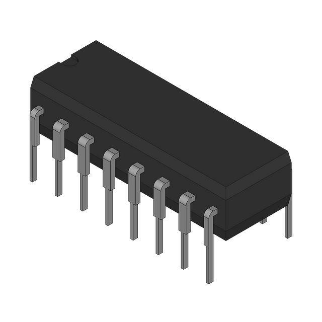
PDIP (16)
(1) For all available packages, see the orderable addendum at
the end of the data sheet.
SN74LV4046A Functional Block Diagram
VCC
16
Phase
Comparator
1
2
13 PC2OUT
3
Phase
Comparator
2
15 PC3OUT
VCOIN
9
Phase
Comparator
3
INH
5
C1A
6
C1B
7
3 Description
The SN74LV4046A is a phase-locked loop (PLL)
circuit that contains a linear voltage-controlled
oscillator (VCO) and three different phase
comparators (PC1, PC2, and PC3). A signal input
and a comparator input are common to each
comparator.
BODY SIZE (NOM)
SN74LV4046ANS
Telecommunications
Signal Generators
Digital Phase-Locked Loop
The SN74LV4046A is a high-speed silicon-gate
CMOS device that is pin compatible with the
CD4046B and the CD74HC4046. The device is
specified in compliance with JEDEC Std 7.
PACKAGE
SIGIN 14
COMPIN
1
4
Voltage
Controlled
Oscillator
PC1OUT
PCPOUT
VCOOUT
10 DEMOUT
R1 11
R2 12
8
GND
1
An IMPORTANT NOTICE at the end of this data sheet addresses availability, warranty, changes, use in safety-critical applications,
intellectual property matters and other important disclaimers. PRODUCTION DATA.
�SN74LV4046A
SCES656E – FEBRUARY 2006 – REVISED NOVEMBER 2016
www.ti.com
Table of Contents
1
2
3
4
5
6
7
Features ..................................................................
Applications ...........................................................
Description .............................................................
Revision History.....................................................
Pin Configuration and Functions .........................
Specifications.........................................................
1
1
1
2
3
4
6.1
6.2
6.3
6.4
6.5
6.6
6.7
4
4
4
4
5
6
9
Absolute Maximum Ratings .....................................
ESD Ratings..............................................................
Recommended Operating Conditions.......................
Thermal Information ..................................................
Electrical Characteristics...........................................
Switching Characteristics ..........................................
Typical Characteristics ..............................................
Detailed Description ............................................ 10
7.1 Overview ................................................................. 10
7.2 Functional Block Diagram ....................................... 10
7.3 Feature Description................................................. 11
7.4 Device Functional Modes........................................ 11
8
Application and Implementation ........................ 12
8.1 Application Information............................................ 12
8.2 Typical Application ................................................. 12
9 Power Supply Recommendations...................... 14
10 Layout................................................................... 14
10.1 Layout Guidelines ................................................. 14
10.2 Layout Example .................................................... 14
11 Device and Documentation Support ................. 15
11.1
11.2
11.3
11.4
11.5
11.6
Documentation Support ........................................
Receiving Notification of Documentation Updates
Community Resources..........................................
Trademarks ...........................................................
Electrostatic Discharge Caution ............................
Glossary ................................................................
15
15
15
15
15
15
12 Mechanical, Packaging, and Orderable
Information ........................................................... 15
4 Revision History
NOTE: Page numbers for previous revisions may differ from page numbers in the current version.
Changes from Revision D (September 2015) to Revision E
Page
•
Deleted 200-V Machine Model (A115-A) from Features ........................................................................................................ 1
•
Added TVSOP and PDIP packages to Device Information table ........................................................................................... 1
•
Added TVSOP, SO, and PDIP packages to pinout ................................................................................................................ 3
•
Changed RθJA for D package from 73°C/W to 82.8°C/W........................................................................................................ 4
•
Changed RθJA for DGV package from 120°C/W to 116.8°C/W .............................................................................................. 4
•
Changed RθJA for NS package from 64°C/W to 83.5°C/W ..................................................................................................... 4
•
Changed RθJA for PW package from 108°C/W to 108.1°C/W ................................................................................................ 4
•
Added values in the Thermal Information table to align with JEDEC standards ................................................................... 4
•
Changed x-axis from "–360° 0° 360°" to "0° 90° 180°" ......................................................................................................... 9
•
Changed "(VCC/4)" to "(VCC/4π)".............................................................................................................................................. 9
•
Added Receiving Notification of Documentation Updates section ....................................................................................... 15
Changes from Revision C (April 2007) to Revision D
•
2
Page
Added Pin Configuration and Functions section, ESD Ratings table, Feature Description section, Device Functional
Modes, Application and Implementation section, Power Supply Recommendations section, Layout section, Device
and Documentation Support section, and Mechanical, Packaging, and Orderable Information section .............................. 1
Submit Documentation Feedback
Copyright © 2006–2016, Texas Instruments Incorporated
Product Folder Links: SN74LV4046A
�SN74LV4046A
www.ti.com
SCES656E – FEBRUARY 2006 – REVISED NOVEMBER 2016
5 Pin Configuration and Functions
D, DGV, NS, N, or PW Package
16-Pin SOIC, TVSOP, SO, PDIP, or TSSOP
Top View
PCPOUT
PC1OUT
COMPIN
VCOOUT
INH
C1A
C1B
GND
1
16
2
15
3
14
4
13
5
12
6
11
7
10
8
9
VCC
PC3OUT
SIGIN
PC2OUT
R2
R1
DEMOUT
VCOIN
Pin Functions
PIN
NO.
1
NAME
I/O
DESCRIPTION
PCPOUT
O
Phase comparator pulse output
2
PC1OUT
O
Phase comparator 1 output
3
COMPIN
I
Comparator input
4
VCOOUT
O
VCO output
Inhibit input
5
INH
I
6
C1A
—
Capacitor C1 connection A
7
C1B
—
Capacitor C1 connection B
8
GND
—
Ground (0 V)
9
VCOIN
I
VCO input
10
DEMOUT
O
Demodulator output
11
R1
—
Resistor R1 connection
12
R2
—
Resistor R2 connection
13
PC2OUT
O
Phase comparator 2 output
14
SIGIN
I
Signal input
15
PC3OUT
O
Phase comparator 3 output
16
VCC
—
Positive supply voltage
Submit Documentation Feedback
Copyright © 2006–2016, Texas Instruments Incorporated
Product Folder Links: SN74LV4046A
3
�SN74LV4046A
SCES656E – FEBRUARY 2006 – REVISED NOVEMBER 2016
www.ti.com
6 Specifications
6.1
Absolute Maximum Ratings
over operating free-air temperature range (unless otherwise noted) (1)
MIN
MAX
UNIT
VCC
DC supply voltage
–0.5
7
V
VI
Input voltage
–0.5
VCC + 0.5
V
VO
Output voltage
–0.5
VCC + 0.5
V
IIK
Input clamp current
VI < 0
–20
mA
IOK
Output clamp current
VO < 0
–50
mA
IO
Continuous output curent
VO = 0 to VCC
±35
mA
ICC
DC VCC or ground current
±70
mA
TJ
Junction temperature
150
°C
Tstg
Storage temperature
150
°C
(1)
–65
Stresses beyond those listed under Absolute Maximum Ratings may cause permanent damage to the device. These are stress ratings
only, and functional operation of the device at these or any other conditions beyond those indicated under Recommended Operating
Conditions is not implied. Exposure to absolute-maximum-rated conditions for extended periods may affect device reliability.
6.2 ESD Ratings
VALUE
V(ESD)
(1)
(2)
Electrostatic discharge
Human body model (HBM), per ANSI/ESDA/JEDEC JS-001 (1)
±2000
Charged-device model (CDM), per JEDEC specification JESD22-C101 (2)
±1000
UNIT
V
JEDEC document JEP155 states that 500-V HBM allows safe manufacturing with a standard ESD control process.
JEDEC document JEP157 states that 250-V CDM allows safe manufacturing with a standard ESD control process.
6.3 Recommended Operating Conditions
over operating free-air temperature range (unless otherwise noted)
MIN
MAX
UNIT
TA
Operating free-air temperature
–40
125
°C
VCC
Supply voltage
3
5.5
V
VI, VO
DC input or output voltage
0
VCC
V
6.4 Thermal Information
SN74LV4046A
THERMAL METRIC (1)
D (SOIC)
DGV (TVSOP)
NS (SO)
PW (TSSOP)
N (PDIP)
16 PINS
16 PINS
16 PINS
16 PINS
16 PINS
UNIT
RθJA
Junction-to-ambient thermal
resistance
82.8
116.8
83.5
108.1
49.4
°C/W
RθJC(top)
Junction-to-case (top) thermal
resistance
44.0
43.3
41.7
42.7
36.7
°C/W
RθJB
Junction-to-board thermal resistance
40.3
48.3
43.8
53.1
29.3
°C/W
ψJT
Junction-to-top characterization
parameter
11.1
3.7
9.3
4.2
21.5
°C/W
ψJB
Junction-to-board characterization
parameter
40.0
47.8
43.5
52.5
29.2
°C/W
(1)
4
For more information about traditional and new thermal metrics, see the Semiconductor and IC Package Thermal Metrics application
report.
Submit Documentation Feedback
Copyright © 2006–2016, Texas Instruments Incorporated
Product Folder Links: SN74LV4046A
�SN74LV4046A
www.ti.com
SCES656E – FEBRUARY 2006 – REVISED NOVEMBER 2016
6.5 Electrical Characteristics
over operating free-air temperature range (unless otherwise noted)
TEST CONDITIONS
PARAMETER
VI (V)
IO (mA)
VCC (V)
MIN
3 to 3.6
VCC × 0.7
4.5 to 5.5
VCC × 0.7
TYP
MAX
UNIT
VCO
VIH
High-level input voltage
INH
VIL
Low-level input voltage
INH
VOH
High-level
output voltage
VCOOUT
VOL
Low-level
output voltage
VCOOUT
CMOS
VIL or VIH
TTL
–12
CMOS
0.05
VIL or VIH
TTL
C1A, C1B
(test purposes only)
II
Input leakage current
–0.05
INH, VCOIN
V
3 to 5.5
VCC × 0.3
4.5 to 5.5
VCC × 0.3
3 to 3.6
VCC – 0.1
4.5 to 5.5
VCC – 0.1
4.5 to 5.5
3.8
V
3 to 3.6
0.1
4.5 to 5.5
0.1
12
4.5 to 5.5
0.55
12
4.5 to 5.5
0.65
VCC or GND
5.5
μA
50
kΩ
3
50
kΩ
40
No Limit
3 to 5.5
R2 range (1)
3 to 5.5
3 to 3.6
4.5 to 5.5
40
No Limit
3 to 3.6
1.1
1.9
4.5 to 5.5
1.1
3.2
Operating voltage range
Over the range specified for
R1 for linearity (2)
VCOIN
V
±1
R1 range (1)
C1 capacitance range
V
3
pF
V
PHASE COMPARATOR
VIH
DC-coupled high-level
input voltage
SIGIN,
COMPIN
VIL
DC-coupled low-level input voltage
VOH
High-level
output voltage
VOL
Low-level
output voltage
PCPOUT,
PCNOUT
PCPOUT,
PCNOUT
SIGIN,
COMPIN
3 to 3.6
VCC × 0.7
4.5 to 5.5
VCC × 0.7
3 to 3.6
VCC × 0.3
4.5 to 5.5
VCC × 0.3
–0.05
3 to 5.5
VCC – 0.1
–6
3 to 3.6
2.48
TTL
–12
4.5 to 5.5
3.8
CMOS
0.02
CMOS
VIL or VIH
VIL or VIH
4
TTL
V
3 to 3.6
0.1
4.5 to 5.5
0.1
4.5 to 5.5
0.4
3 to 3.6
±11
4.5 to 5.5
±29
II
Input leakage current
SIGIN,
COMPIN
IOZ
3-state off-state current
PC2OUT
VIL or VIH
Input resistance
SIGIN,
COMPIN
VI at self-bias operating
point, VI = 0.5 V
3
800
4.5
250
RS > 300 kΩ, Leakage
current can influence
VDEMOUT
3 to 3.6
50
300
4.5 to 5.5
50
300
VI = VVCOIN = VCC/2, Values
taken over RS range
3 to 3.6
±30
4.5 to 5.5
±20
RI
VCC or GND
V
3 to 5.5
±5
V
μA
μA
kΩ
DEMODULATOR
RS
Resistor range
VOFF
Offset voltage VCOIN to VDEM
ICC
Quiescent device current
(1)
(2)
Pins 3, 5, and 14 at VCC,
Pin 9 at GND, II at pins 3
and 14 to be excluded
5.5
kΩ
mV
50
μA
The value for R1 and R2 in parallel should exceed 2.7 kΩ.
The maximum operating voltage can be as high as VCC – 0.9 V; however, this may result in an increased offset voltage.
Submit Documentation Feedback
Copyright © 2006–2016, Texas Instruments Incorporated
Product Folder Links: SN74LV4046A
5
�SN74LV4046A
SCES656E – FEBRUARY 2006 – REVISED NOVEMBER 2016
www.ti.com
6.6 Switching Characteristics
over operating free-air temperature range (unless otherwise noted) CL = 50 pF, Input tr, tf = 6 ns
PARAMETER
VCC
(V)
TEST CONDITIONS
MIN
TYP
MAX
UNIT
PHASE COMPARATOR
tPLH, tPHL
Propagation delay
SIGIN, COMPIN to
PC1OUT
3 to 3.6
135
4.5 to 5.5
50
tPLH, tPHL
Propagation delay
SIGIN, COMPIN to
PCPOUT
3 to 3.6
300
4.5 to 5.5
60
tPLH, tPHL
Propagation delay
SIGIN, COMPIN to
PC3OUT
3 to 3.6
200
4.5 to 5.5
50
tTHL, tTLH
Output transition time
tPZH, tPZL
3-state output enable time
SIGIN, COMPIN to
PC2OUT
tPHZ, tPLZ
3-state output disable time
SIGIN, COMPIN to
PC2OUT
AC-coupled input sensitivity
(P-P) at SIGIN or
COMPIN
VI(P-P)
3 to 3.6
75
4.5 to 5.5
15
3 to 3.6
270
4.5 to 5.5
54
3 to 3.6
320
4.5 to 5.5
65
3 to 3.6
11
4.5 to 5.5
15
ns
ns
ns
ns
ns
ns
mV
VCO
Frequency stability with temperature change
Δf/ΔT
fMAX
Maximum frequency
Center frequency (duty 50%)
ΔfVCO
VI = VCOIN = 1/2 VCC,
R1 = 100 kΩ,
R2 = ∞,
C1 = 100 pF
C1 = 50 pF,
R1 = 3.5 kΩ,
R2 = ∞
C1 = 0 pF,
R1 = 9.1 kΩ,
R2 = ∞
C1 = 40 pF,
R1 = 3 kΩ,
R2 = ∞,
VCOIN = VCC/2
3 to 3.6
0.11
4.5 to 5.5
0.11
3 to 3.6
24
4.5 to 5.5
24
3 to 3.6
38
4.5 to 5.5
38
3 to 3.6
4.5 to 5.5
4.5 (1)
7
10
12
17
15 (1)
%/°C
MHz
MHz
17.5 (1)
C1 = 100 pF,
R1 = 100 kΩ,
R2 = ∞
3 to 3.6
0.4%
Frequency linearity
4.5 to 5.5
0.4%
Offset frequency
C1 = 1 nF,
R2 = 220 kΩ
3 to 3.6
400
4.5 to 5.5
400
kHz
DEMODULATOR
VOUT vs fIN
(1)
6
C1 = 100 pF,
C2 = 100 pF,
R1 = 100 kΩ,
R2 = ∞,
R3 = 100 kΩ
3
4.5
8
330
mV/kHz
Data is specified at 25°C
Submit Documentation Feedback
Copyright © 2006–2016, Texas Instruments Incorporated
Product Folder Links: SN74LV4046A
�SN74LV4046A
www.ti.com
SCES656E – FEBRUARY 2006 – REVISED NOVEMBER 2016
SIGIN
COMPIN
VCOOUT
PC1OUT
VCC
VCOIN
GND
Loop Locked at fo
Figure 1. Typical Waveforms for PLL Using
Phase Comparator 1
SIGIN
COMPIN
VCOOUT
VCC
GND
PC2 OUT
High-Impedance Off State
VCO IN
PCPOUT
Loop Locked at fo
Figure 2. Typical Waveforms for PLL Using
Phase Comparator 2
SIGIN
COMPIN
VCOOUT
PC3OUT
VCC
VCOIN
GND
Loop Locked at fo
Figure 3. Typical Waveforms for PLL Using
Phase Comparator 3
Submit Documentation Feedback
Copyright © 2006–2016, Texas Instruments Incorporated
Product Folder Links: SN74LV4046A
7
�SN74LV4046A
SCES656E – FEBRUARY 2006 – REVISED NOVEMBER 2016
www.ti.com
SIGIN, COMPIN
Inputs
VS
tPHL
PCPOUT, PC1OUT,
PC3OUT
Outputs
tPLH
VS
tTHL
tTLH
Figure 4. Input-to-Output Propagation Delays and
Output Transition Times
SIGIN
Inputs
VS
COMPIN
Inputs
VS
tPHZ
tPZL
tPZH
PC2OUT
Output
tPLZ
90%
VS
10%
Figure 5. 3-State Enable and Disable Times for PC2OUT
8
Submit Documentation Feedback
Copyright © 2006–2016, Texas Instruments Incorporated
Product Folder Links: SN74LV4046A
�SN74LV4046A
www.ti.com
SCES656E – FEBRUARY 2006 – REVISED NOVEMBER 2016
6.7 Typical Characteristics
VCC
VCC
V DEMOUT (AV)
V DEMOUT (AV)
1/2 V CC
1/2 V CC
0
0
φDEMOUT
0°
90°
Phase Comparator 1:
VDEMOUT = VPC1OUT = (VCC/π) (SIGIN – COMPIN);
DEMOUT = (SIGIN – COMPIN)
180°
Figure 6. Average Output Voltage vs Input Phase Difference
φDEMOUT
-360°
0°
Phase Comparator 2:
VDEMOUT = VPC2OUT = (VCC/4π) (SIGIN – COMPIN);
DEMOUT = (SIGIN – COMPIN)
360°
Figure 7. Average Output Voltage vs Input Phase Difference
VCC
VDEMOUT(AV)
1/2 VCC
0
0°
180° φDEMOUT
360°
Phase Comparator 3:
VDEMOUT = VPC3OUT = (VCC/2π) (SIGIN – COMPIN);
DEMOUT = (SIGIN – COMPIN)
Figure 8. Average Output Voltage vs Input Phase Difference
Submit Documentation Feedback
Copyright © 2006–2016, Texas Instruments Incorporated
Product Folder Links: SN74LV4046A
9
�SN74LV4046A
SCES656E – FEBRUARY 2006 – REVISED NOVEMBER 2016
www.ti.com
7 Detailed Description
7.1 Overview
The SN74LV4046A is a high-speed silicon-gate CMOS device that is pin compatible with the CD4046B and the
CD74HC4046. The device is specified in compliance with JEDEC Std 7.
The SN74LV4046A is a phase-locked loop (PLL) circuit that contains a linear voltage-controlled oscillator (VCO)
and three different phase comparators (PC1, PC2, and PC3) as explained in the Features section. A signal input
and a comparator input are common to each comparator as shown in the Functional Block Diagram.
The signal input can be directly coupled to large voltage signals, or indirectly coupled (with a series capacitor) to
small voltage signals. A self-bias input circuit keeps small voltage signals within the linear region of the input
amplifiers. With a passive lowpass filter, the SN74LV4046A forms a second-order loop PLL. The excellent VCO
linearity is achieved by the use of linear operational amplifier techniques. Various applications include
telecommunications, Digital Phase Locked Loop and Signal generators.
The VCO requires one external capacitor C1 (between C1A and C1B) and one external resistor R1 (between R1
and GND) or two external resistors R1 and R2 (between R1 and GND, and R2 and GND). Resistor R1 and
capacitor C1 determine the frequency range of the VCO. Resistor R2 enables the VCO to have a frequency
offset if required. The high input impedance of the VCO simplifies the design of lowpass filters by giving the
designer a wide choice of resistor or capacitor ranges. In order to not load the lowpass filter, a demodulator
output of the VCO input voltage is provided at pin 10 (DEMOUT). In contrast to conventional techniques where the
DEMOUT voltage is one threshold voltage lower than the VCO input voltage, here the DEMOUT voltage equals that
of the VCO input. If DEMOUT is used, a load resistor (RS) should be connected from DEMOUT to GND; if unused,
DEMOUT should be left open. The VCO output (VCOOUT) can be connected directly to the comparator input
(COMPIN), or connected through a frequency divider. The VCO output signal has a specified duty factor of 50%.
A LOW level at the inhibit input (INH) enables the VCO and demodulator, while a HIGH level turns both off to
minimize standby power consumption.
7.2 Functional Block Diagram
VCC
16
Phase
Comparator
1
2
13 PC2OUT
3
Phase
Comparator
2
15 PC3OUT
VCOIN
9
Phase
Comparator
3
INH
5
SIGIN 14
COMPIN
C1A
6
C1B
7
1
4
Voltage
Controlled
Oscillator
PC1OUT
PCPOUT
VCOOUT
10 DEMOUT
R1 11
R2 12
8
GND
10
Submit Documentation Feedback
Copyright © 2006–2016, Texas Instruments Incorporated
Product Folder Links: SN74LV4046A
�SN74LV4046A
www.ti.com
SCES656E – FEBRUARY 2006 – REVISED NOVEMBER 2016
7.3 Feature Description
There are three choices for the Phase Comparators in this device which are listed as follows:
• Phase comparator 1 (PC1) is an Exclusive OR network. The average output voltage from PC1, fed to VCO
input through the low pass filter and seen at the demodulator output at pin 10 (VDEMOUT), is the resultant of
the phase differences of signals (SIGIN) and the compartor input (COMPIN) as shown in Figure 7. The
average of V DEM is equal to 1/2 VCC when there is no signal or noise at SIGIN, and with this input the VCO
oscillates at the center frequency (fo).
• Phase comparator 2 (PC2) is an Edge-Triggered Flip-Flop. This is a positive edge-triggered phase and
frequency detector. When the PLL is using this comparator, the loop is controlled by positive signal transitions
and the duty factors of SIGIN and COMPIN are not important. PC2 comprises two D-type flip-flops, controlgating and a three-state output stage. The circuit functions as an up-down counter where SIGIN causes an upcount and COMPIN a down-count. The average output voltage from PC2, fed to the VCO through the lowpass
filter and seen at the demodulator output at pin 10 (VDEMOUT), is the resultant of the phase differences of
SIGIN and COMPINas in Figure 8.
• Phase comparator 3 (PC3) is an positive Edge-Triggered RS Flip-Flop. This is a positive edge-triggered
sequential phase detector using an RS-type flip-flop. When the PLL is using this comparator, the loop is
controlled by positive signal transitions and the duty factors of SIGIN and COMPIN are not important. The
average output from PC3, fed to the VCO through the lowpass filter and seen at the demodulator at pin 10
(VDEMOUT), is the resultant of the phase differences of SIGIN and COMPIN as shown in Figure 9.
The excellent VCO linearity is achieved by the use of linear operational amplifier techniques. It has low standby
power consumption using VCO inhibit control. Wide operating temperature range from –40°C to +125°C along
with an optimized power supply voltage range from 3 V to 5.5 V.
7.4 Device Functional Modes
The SN74LV4046A device does not feature any special functional modes.
Submit Documentation Feedback
Copyright © 2006–2016, Texas Instruments Incorporated
Product Folder Links: SN74LV4046A
11
�SN74LV4046A
SCES656E – FEBRUARY 2006 – REVISED NOVEMBER 2016
www.ti.com
8 Application and Implementation
NOTE
Information in the following applications sections is not part of the TI component
specification, and TI does not warrant its accuracy or completeness. TI’s customers are
responsible for determining suitability of components for their purposes. Customers should
validate and test their design implementation to confirm system functionality.
8.1 Application Information
The most common use for the digital phased-locked loop (PLL) device is to match the VCO output to the same
phase as the incoming signal and produce an error signal (DEMOUT) that indicates the amount of phase shift
required for the match. This can be used as part of many complex systems.
8.2 Typical Application
VCC
16
SIGIN
Input
COMPIN
VCOOUT
INH
C1A
C1
C1B
R1
R2
R1
R2
14
3
4
Phase
Comparator
1
2
Phase
Comparator
2
13
Phase
Comparator
3
5
6
7
1
15
9
Voltage
Controlled
Oscillator
10
PC1OUT
PC2OUT
R3
PCPOUT
C2
PC3OUT
VCOIN
DEMOUT
R5
11
12
8
GND
Figure 9. SN74LV4046A Digital Clock Signal Phase Comparison Application
12
Submit Documentation Feedback
Copyright © 2006–2016, Texas Instruments Incorporated
Product Folder Links: SN74LV4046A
�SN74LV4046A
www.ti.com
SCES656E – FEBRUARY 2006 – REVISED NOVEMBER 2016
Typical Application (continued)
8.2.1 Design Requirements
Table 1 and Table 2 lists the design requirements of the SN74LV4046A.
Table 1. Component Selection Criteria (1)
(1)
COMPONENT
VALUE
R1
3 kΩ to 50 kΩ
R2
3 kΩ to 50 kΩ
R1 || R2
> 2.7 kΩ
C1
> 40 pF
R3
1 kΩ
C2
1 uF
R5
50 kΩ to 300 kΩ
R1 between 3 kΩ and 50 kΩ
R2 between 3 kΩ and 50 kΩ
R1 + R2 parallel value > 2.7 kΩ
C1 > 40 pF
Table 2. CPD (1)
CHIP SECTION
CPD
Comparator 1
120
VCO
120
(1)
UNIT
pF
R1 between 3 kΩ and 50 kΩ
R2 between 3 kΩ and 50 kΩ
R1 + R2 parallel value > 2.7 kΩ
C1 > 40 pF
8.2.2 Detailed Design Procedure
1. Recommended Input Conditions:
– VIH and VIL for each input can be found in Electrical Characteristics.
2. Recommended Output Conditions:
– Valid load resistor values are specified in Electrical Characteristics.
3. Frequency Selection Criterion:
– Frequency data is found in Electrical Characteristics.
8.2.3 Application Curves
Table 3 lists the application curves in the Typical Characteristics section.
Table 3. Table of Graphs
GRAPH TITLE
FIGURE
Average Output Voltage vs Input Phase Difference
Figure 6
Average Output Voltage vs Input Phase Difference
Figure 7
Average Output Voltage vs Input Phase Difference
Figure 8
Submit Documentation Feedback
Copyright © 2006–2016, Texas Instruments Incorporated
Product Folder Links: SN74LV4046A
13
�SN74LV4046A
SCES656E – FEBRUARY 2006 – REVISED NOVEMBER 2016
www.ti.com
9 Power Supply Recommendations
The power supply can be any voltage between the minimum and maximum supply voltage ratings located in the
Recommended Operating Conditions table.
Each VCC pin should have a good bypass capacitor to prevent power disturbance. For devices with a single
supply. a 0.1-µF capacitor is recommended and if there are multiple VCC pins then 0.01-µF or 0.022-µF capacitor
is recommended for each power pin. It is ok to parallel multiple bypass capacitors to reject different frequencies
of noise. 0.1-µF and 1-µF capacitors are commonly used in parallel. The bypass capacitor should be installed as
close to the power pin as possible for best results.
10 Layout
10.1 Layout Guidelines
Reflections and matching are closely related to the loop antenna theory but are different enough to be discussed
separately from the theory. When a PCB trace turns a corner at a 90° angle, a reflection can occur. A reflection
occurs primarily because of the change of width of the trace. At the apex of the turn, the trace width increases to
1.414 times the width. This increase upsets the transmission-line characteristics, especially the distributed
capacitance and self–inductance of the trace which results in the reflection. Not all PCB traces can be straight
and therefore some traces must turn corners. Figure 10 shows progressively better techniques of rounding
corners. Only the last example (BEST) maintains constant trace width and minimizes reflections.
10.2 Layout Example
BETTER
BEST
2W
WORST
1W min.
W
Figure 10. Trace Example
14
Submit Documentation Feedback
Copyright © 2006–2016, Texas Instruments Incorporated
Product Folder Links: SN74LV4046A
�SN74LV4046A
www.ti.com
SCES656E – FEBRUARY 2006 – REVISED NOVEMBER 2016
11 Device and Documentation Support
11.1 Documentation Support
11.1.1 Related Documentation
For related documentation see the following:
Implications of Slow or Floating CMOS Inputs, SCBA004
11.2 Receiving Notification of Documentation Updates
To receive notification of documentation updates, navigate to the device product folder on ti.com. In the upper
right corner, click on Alert me to register and receive a weekly digest of any product information that has
changed. For change details, review the revision history included in any revised document.
11.3 Community Resources
The following links connect to TI community resources. Linked contents are provided "AS IS" by the respective
contributors. They do not constitute TI specifications and do not necessarily reflect TI's views; see TI's Terms of
Use.
TI E2E™ Online Community TI's Engineer-to-Engineer (E2E) Community. Created to foster collaboration
among engineers. At e2e.ti.com, you can ask questions, share knowledge, explore ideas and help
solve problems with fellow engineers.
Design Support TI's Design Support Quickly find helpful E2E forums along with design support tools and
contact information for technical support.
11.4 Trademarks
E2E is a trademark of Texas Instruments.
All other trademarks are the property of their respective owners.
11.5 Electrostatic Discharge Caution
These devices have limited built-in ESD protection. The leads should be shorted together or the device placed in conductive foam
during storage or handling to prevent electrostatic damage to the MOS gates.
11.6 Glossary
SLYZ022 — TI Glossary.
This glossary lists and explains terms, acronyms, and definitions.
12 Mechanical, Packaging, and Orderable Information
The following pages include mechanical, packaging, and orderable information. This information is the most
current data available for the designated devices. This data is subject to change without notice and revision of
this document. For browser-based versions of this data sheet, refer to the left-hand navigation.
Submit Documentation Feedback
Copyright © 2006–2016, Texas Instruments Incorporated
Product Folder Links: SN74LV4046A
15
�PACKAGE OPTION ADDENDUM
www.ti.com
14-Oct-2022
PACKAGING INFORMATION
Orderable Device
Status
(1)
Package Type Package Pins Package
Drawing
Qty
Eco Plan
(2)
Lead finish/
Ball material
MSL Peak Temp
Op Temp (°C)
Device Marking
(3)
Samples
(4/5)
(6)
SN74LV4046AD
ACTIVE
SOIC
D
16
40
RoHS & Green
NIPDAU
Level-1-260C-UNLIM
-40 to 85
LV4046A
Samples
SN74LV4046ADGVR
ACTIVE
TVSOP
DGV
16
2000
RoHS & Green
NIPDAU
Level-1-260C-UNLIM
-40 to 85
LW046A
Samples
SN74LV4046ADR
ACTIVE
SOIC
D
16
2500
RoHS & Green
NIPDAU
Level-1-260C-UNLIM
-40 to 85
LV4046A
Samples
SN74LV4046AN
ACTIVE
PDIP
N
16
25
RoHS & Green
NIPDAU
N / A for Pkg Type
-40 to 85
SN74LV4046AN
Samples
SN74LV4046ANS
ACTIVE
SO
NS
16
50
RoHS & Green
NIPDAU
Level-1-260C-UNLIM
-40 to 85
74LV4046A
Samples
SN74LV4046ANSR
ACTIVE
SO
NS
16
2000
RoHS & Green
NIPDAU
Level-1-260C-UNLIM
-40 to 85
74LV4046A
Samples
SN74LV4046APW
ACTIVE
TSSOP
PW
16
90
RoHS & Green
NIPDAU
Level-1-260C-UNLIM
-40 to 85
LW046A
Samples
SN74LV4046APWG4
ACTIVE
TSSOP
PW
16
90
RoHS & Green
NIPDAU
Level-1-260C-UNLIM
-40 to 85
LW046A
Samples
SN74LV4046APWR
ACTIVE
TSSOP
PW
16
2000
RoHS & Green
NIPDAU
Level-1-260C-UNLIM
-40 to 85
LW046A
Samples
(1)
The marketing status values are defined as follows:
ACTIVE: Product device recommended for new designs.
LIFEBUY: TI has announced that the device will be discontinued, and a lifetime-buy period is in effect.
NRND: Not recommended for new designs. Device is in production to support existing customers, but TI does not recommend using this part in a new design.
PREVIEW: Device has been announced but is not in production. Samples may or may not be available.
OBSOLETE: TI has discontinued the production of the device.
(2)
RoHS: TI defines "RoHS" to mean semiconductor products that are compliant with the current EU RoHS requirements for all 10 RoHS substances, including the requirement that RoHS substance
do not exceed 0.1% by weight in homogeneous materials. Where designed to be soldered at high temperatures, "RoHS" products are suitable for use in specified lead-free processes. TI may
reference these types of products as "Pb-Free".
RoHS Exempt: TI defines "RoHS Exempt" to mean products that contain lead but are compliant with EU RoHS pursuant to a specific EU RoHS exemption.
Green: TI defines "Green" to mean the content of Chlorine (Cl) and Bromine (Br) based flame retardants meet JS709B low halogen requirements of


 工商网监
湘ICP备2023018690号
工商网监
湘ICP备2023018690号
