��������
���
�
��������������
� ���
����
www.ti.com
SCLS591A − SEPTEMBER 2004 − REVISED APRIL 2008
DESCRIPTION
The SN74LV8153 is a serial-to-parallel data converter. It
accepts serial input data and outputs 8-bit parallel data.
The automatic data-rate detection feature of the
SN74LV8153 eliminates the need for an external oscillator
and helps with cost and board real-estate savings.
The OUTSEL pin is used to choose between open
collector and push-pull outputs. The open-collector option
is suitable when this device is used in applications such as
LED interface, where high drive current is required. SOUT
is the output that acknowledges reception of the serial
data.
To ensure the high-impedance state during power up or
power down, OE should be tied to VCC1 through a pullup
resistor; the minimum value of the resistor is determined
by the current-sinking capability of the driver.
FEATURES
D Qualified for Automotive Applications
D Single-Wire Serial Data Input
D Compatible With UART Serial-Data Format
D Up to Eight Devices (64-Bit Parallel) Can
Share the Same Bus by Using Different
Combinations of A0, A1, A2
D Up to 40 mA Current Drive in Open-Collector
Mode for Driving LEDs
D Outputs Can be Configured as
Open-Collector or Push-Pull
D Internal Oscillator and Counter for
D
D
D
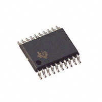
PW PACKAGE
(TOP VIEW)
VCC1
A0
A1
A2
D
OUTSEL
RESET
OE
SOUT
GND
1
20
2
19
3
18
4
17
5
16
6
15
7
14
8
13
9
12
10
11
VCC2
Y0
Y1
Y2
Y3
Y4
Y5
Y6
Y7
GND
Automatic Data-Rate Detection
Output Levels Are Referenced to VCC2 and
Can Be Configured From 3 V to 12 V
Latch-Up Performance Exceeds 250 mA Per
JESD 17
ESD Protection Exceeds JESD 22
− 2000-V Human-Body Model (A114-A)
− 1000-V Charged-Device Model (C101)
SUMMARY OF RECOMMENDED
OPERATING CONDITIONS
PARAMETER
VCC1
VCC2
3 V to 5.5 V
3 V to 13.2 V
IOL
40 mA @ VCC2 = 4.5 V
(open-collector mode)
IOH
−24 mA @ VCC2 = 12 V
(push-pull mode)
Maximum Data Rate
24 Kbps
Please be aware that an important notice concerning availability, standard warranty, and use in critical applications of Texas Instruments
semiconductor products and disclaimers thereto appears at the end of this data sheet.
���������� ���� ����������� �! "#��$�� �! �� %#&'�"����� (��$) ���(#"�!
"������ �� !%$"���"�����! %$� �*$ �$��! �� �$+�! ��!��#�$��! !���(��( ,������-)
���(#"���� %��"$!!��. (�$! ��� �$"$!!���'- ��"'#($ �$!���. �� �'' %����$�$�!)
Copyright 2008, Texas Instruments Incorporated
���������
���
�
��������������
� ���
����
www.ti.com
SCLS591A − SEPTEMBER 2004 − REVISED APRIL 2008
FUNCTION TABLE
(each buffer)
INPUTS
OUTPUT
Yn
OUTSEL
RESET
OE
Dn
L
H
L
H
L
L
H
L
L
H
L
X
H
X
H
L
L
X
X
H
H
H
L
H
H
H
H
L
L
L
H
X
H
X
Z
H
L
L
X
L
OUTPUT
STRUCTURE
Open collector
Push-pull
In the open-collector mode (OUTSEL = L), the outputs are inverted,
e.g., Y1 = l, when D1 = H
ORDERING INFORMATION {
PACKAGE}
TA
ORDERABLE
PART NUMBER
TOP-SIDE
MARKING
−40°C to 125°C
TSSOP − PW
Tape and reel
SN74LV8153QPWRQ1
LV8153Q
† For the most current package and ordering information, see the Package Option Addendum at the end of this document, or
see the TI web site at http://www.ti.com.
‡ Package drawings, thermal data, and symbolization are available at http://www.ti.com/packaging.
PIN DESCRIPTION
PIN #
I/O
PIN FUNCTION
VCC1
Power-supply pin (all inputs and outputs except for Y0-Y7)
A0, A1, A2
In
The address pins are used to program the address of the device and allow up to eight
devices to share the same bus.
5
D
In
Serial data input
6
OUTSEL
In
Choose between open-collector and push-pull type outputs (Y0-Y7).
7
RESET
In
Initialize register status
8
OE
In
Force Y0-Y7 to Hi-Z
1
2-4
2
PIN NAME
9
SOUT
Out
Outputs a pulse when latch data is changed. Supplied by VCC1.
12-19
Y0-Y7
Out
Push-pull or open collector parallel data outputs. Supplied by VCC2.
20
VCC2
Power-supply pin for outputs (Y0-Y7). VCC2 can range from 3 V to 13.2 V.
���������
���
�
��������������
� ���
����
www.ti.com
SCLS591A − SEPTEMBER 2004 − REVISED APRIL 2008
data transmission protocol
− The serial data should be sent as 2START-3ADDRESS-4DATA-1STOP. Two consecutive serial-data
frames transmit 8 bits of data. The first frame includes the lower four bits of data (D0-D3), and the
second frame includes the upper four bits (D4-D7).
− The three address bits (in the consecutive frame) must be the same as those in the first frame;
otherwise, the data will be dropped.
− The order of the two start bits must be 0, then 1 in any frame; otherwise, the data rate will not be
detected correctly. The period between the falling edge of the first start bit (ST0) and the rising edge of
the second start bit (ST1) is measured to generate an internal-clock synchronized data stream.
1st Frame
ST0
A0
A1
A2
2nd Frame
D0
D1
D2
ST0
D3
ST1
SP
A0
A1
A2
D4
D5
D6
D7
ST1
SP
Example of Serial-Data Format
ST0
DATA
ST0
ST1
A0
A1
A2
D0
D1
D2
D3
SP
ST1
A0
A1
A2
D4
D5
D6
D7
SP
Internal Clock
Y0−Y7
SOUT
Timing Chart
(1)Internal clock cannot be observed.
(1)D0 is LSB and D7 is MSB. The data stream should be LSB first.
3
���������
���
�
��������������
� ���
����
www.ti.com
SCLS591A − SEPTEMBER 2004 − REVISED APRIL 2008
logic diagram
Power
On
Reset
Data
8-Bit S/R
CLK
OC
Timing
Control
4
Y0
4
8-Bit Register
Timing
and
Address
Verification
4-Bit Register
4 Data
OC
Y7
3
OSC
3
Address Data
A0
A1
A2
3-Bit
Register
SOUT
RESET
OUTSEL
OE
absolute maximum ratings over operating free-air temperature range (unless otherwise noted)(1)
Supply voltage range, VCC1 . . . . . . . . . . . . . . . . . . . . . . . . . . . . . . . . . . . . . . . . . . . . . . . . . . . . . . . . −0.5 V to 7 V
Supply voltage range, VCC2 . . . . . . . . . . . . . . . . . . . . . . . . . . . . . . . . . . . . . . . . . . . . . . . . . . . . . . −0.5 V to 14.5 V
Input voltage range, VI(2) . . . . . . . . . . . . . . . . . . . . . . . . . . . . . . . . . . . . . . . . . . . . . . . . . . . . . . . . . . . −0.5 V to 7 V
Voltage range applied to any output in the high or low state, VO (SOUT) (2)(3) . . . . −0.5 V to VCC1 + 0.5 V
Voltage range applied to any output in the high-impedance
or power-off state, VO (SOUT) (2) . . . . . . . . . . . . . . . . . . . . . . . . . . . . . . . . . . . . . . . . . . . . . . . . . −0.5 V to 7 V
Voltage range, applied to any output in the high or low state, VO (Y0-Y7)(2)(3) . . . . −0.5 V to VCC2 + 0.5 V
Voltage range applied to any output in the high-impedance
or power-off state, VO (Y0-Y7)(2) . . . . . . . . . . . . . . . . . . . . . . . . . . . . . . . . . . . . . . . . . . . . . . . . −0.5 V to 14.5 V
Input clamp current, IIK (VI < 0) . . . . . . . . . . . . . . . . . . . . . . . . . . . . . . . . . . . . . . . . . . . . . . . . . . . . . . . . . . −20 mA
Output clamp current, IOK (VO < 0) . . . . . . . . . . . . . . . . . . . . . . . . . . . . . . . . . . . . . . . . . . . . . . . . . . . . . . . −50 mA
Continuous output current, IO (VO = 0 to VCC) . . . . . . . . . . . . . . . . . . . . . . . . . . . . . . . . . . . . . . . . . . . . . . 25 mA
Continuous current, IO (OUTSEL = L, Y0-Y7 = L) . . . . . . . . . . . . . . . . . . . . . . . . . . . . . . . . . . . . . . . . . . . 60 mA
Package thermal impedance, θJA(4) . . . . . . . . . . . . . . . . . . . . . . . . . . . . . . . . . . . . . . . . . . . . . . . . . . . . . . 83°C/W
Storage temperature range, Tstg . . . . . . . . . . . . . . . . . . . . . . . . . . . . . . . . . . . . . . . . . . . . . . . . . . −65°C to 150°C
(1) Stresses beyond those listed under “absolute maximum ratings” may cause permanent damage to the device. These are stress ratings only, and
functional operation of the device at these or any other conditions beyond those indicated under “recommended operating conditions” is not
implied. Exposure to absolute-maximum-rated conditions for extended periods may affect device reliability.
(2)The input and output voltage ratings may be exceeded if the input and output current ratings are observed.
(3)The value of VCC is provided in the recommended operating condition table.
(4)The package thermal impedance is calculated in accordance with JESD 51-7.
4
���������
���
�
��������������
� ���
����
www.ti.com
SCLS591A − SEPTEMBER 2004 − REVISED APRIL 2008
recommended operating conditions(1)
VCC1
VCC1
VCC2
UNIT
3
5.5
V
3
13.2
V
VIL
Low-level input voltage
VI
Input voltage
OUTSEL = H
High-level output current
SOUT
OUTSEL = H
Yn
Low-level output current
OUTSEL = L
SOUT
VCC × 0.7
VCC × 0.7
3V
3V
4.5 V
4.5 V
3V
3V
4.5 V
4.5 V
0
5.5
4.5 V
4.5 V
0
5.5
12 V
0
13.2
Output voltage
Yn
IOL
MAX
Supply voltage
High-level input voltage
IOH
MIN
Supply voltage
VIH
VO
VCC2
V
VCC × 0.3
VCC × 0.3
3V
3V
−2
4.5 V
4.5 V
−8
4.5 V
12 V
−24
3V
3V
−4
4.5 V
4.5 V
−8
3V
3V
4.5 V
4.5 V
3V
3V
20
4.5 V
4.5 V
40
3V
3V
4
4.5 V
4.5 V
8
V
V
V
mA
mA
2
8
mA
TA
Operating free-air temperature
−40
125
°C
(1) All unused inputs of the device must be held at VCC or GND to ensure proper device operation. Refer to the TI application report, Implications
of Slow or Floating CMOS Inputs, literature number SCBA004.
5
���������
���
�
��������������
� ���
����
www.ti.com
SCLS591A − SEPTEMBER 2004 − REVISED APRIL 2008
electrical characteristics over recommended operating free-air temperature range (unless
otherwise noted)
PARAMETER
TEST CONDITIONS
VT+
Positive-going input threshold
voltage
All inputs
VT−
Negative-going input threshold
voltage
All inputs
∆VT
Hysteresis
(VT+ − VT−)
All inputs
VOH
SOUT
Yn
VOL
SOUT
TYP
MAX
VCC2
3.3 V
3.3 V
2.31
5V
5V
3.5
3.3 V
3.3 V
0.99
5V
5V
1.5
3.3 V
3.3 V
0.33
1.32
5V
5V
0.5
2
UNIT
V
V
V
IOH = −2 mA
IOH = −8 mA
Yn
MIN
VCC1
3V
3V
2.38
4.5 V
4.5 V
3.8
IOH = −24 mA
IOH = −4 mA
4.5 V
12 V
11
3V
3V
2.38
IOH = −8 mA
IOL = 2 mA (OUTSEL = H)
4.5 V
4.5 V
3.8
3V
3V
0.44
IOL = 8 mA (OUTSEL = H)
IOL = 40 mA (OUTSEL = L)
4.5 V
4.5 V
0.44
4.5 V
4.5 V
0.5
3V
3V
0.44
4.5 V
4.5 V
0.44
IOL = 4 mA
IOL = 8 mA
II
IOZ
VI = 5.5 V or GND
VO = VCC or GND (OUTSEL = H)
IOH
VO = 12 V (OUTSEL = L)
V
0 to 5.5 V
±1
µA
5.5 V
5.5 V
±5
µA
5.5 V
5.5 V
5
µA
OUTSEL = H
ICC
VI = VCC or GND, IO = 0
Ioff (except SOUT)
Ci
VI or VO = 0 to 5.5 V, VCC = 0
VI = VCC or GND
OUTSEL = L
V
5
5.5 V
5.5 V
0
0
5V
5V
20
±50
5
mA
µA
pF
switching characteristics over recommended operating free-air temperature
VCC1 = VCC2 = 3.3 V ± 0.3 V (unless otherwise noted) (see Figures 1 and 2)
range,
FROM
(INPUT)
TO
(OUTPUT)
D7
Y
TA = 25°C
MIN
TYP
MAX
(1)
Pw/2
D7
SOUT
Pw/2
RESET
OE(2)
Y
ten
OE(3)
Y
220
ns
tdis
OE(3)
Y
220
ns
PARAMETER
tpd
tw
Y
SOUT
Data rate
LOAD
CAPACITANCE
MIN
MAX
UNIT
(1)
220
ns
220
CL = 50 pF
Pw
(4)
ns
2
24
Kbps
(1) The t
pd is dependent on the data pulse width (Pw), and Y outputs are changed after one-half of Pw, because the internal clock is synchronized
at the middle of the data pulse. Not tested, but specified by design.
(2) When outputs are open collector (OUTSEL = L)
(3) When outputs are push-pull (OUTSEL = H)
(4) SOUT goes low when the data is received correctly and maintains a low level for one data-pulse period. Not tested, but specified by design.
6
���������
���
�
��������������
� ���
����
www.ti.com
SCLS591A − SEPTEMBER 2004 − REVISED APRIL 2008
switching characteristics over recommended operating free-air temperature
VCC1 = VCC2 = 5 V ± 0.5 V (unless otherwise noted) (see Figures 1 and 2)
PARAMETER
FROM
(INPUT)
TO
(OUTPUT)
D7
Y
D7
SOUT
RESET
OE(2)
Y
ten
OE(3)
Y
tdis
OE(3)
Y
tpd
tw
Data rate
Y
SOUT
LOAD
CAPACITANCE
MIN
TA = 25°C
TYP
MAX
(1)
Pw/2
Pw/2
MIN
MAX
range,
UNIT
(1)
200
ns
200
CL = 50 pF
Pw
200
ns
200
ns
(4)
ns
2
24
Kbps
(1) The tpd is dependent on the data pulse width (Pw), and Y outputs are changed after one-half of Pw, because the internal clock is synchronized
at the middle of the data pulse. Not tested, but specified by design.
(2) When outputs are open collector (OUTSEL = L)
(3) When outputs are push-pull (OUTSEL = H)
(4) SOUT goes low when the data is received correctly and maintains a low level for one data-pulse period. Not tested, but specified by design.
7
���������
���
�
��������������
� ���
����
www.ti.com
SCLS591A − SEPTEMBER 2004 − REVISED APRIL 2008
PARAMETER MEASUREMENT INFORMATION
(PUSH-PULL OUTPUT)
From Output
Under Test
CL = 50 pF
(see Note A)
RL = 1 kΩ
VCC1
Open
S1
50% VCC1
tPLH
tPHL
Out-of-Phase
Output
0V
VOH
50% VCC1
VOL
VOH
50% VCC1
VOL
VOLTAGE WAVEFORMS
PROPAGATION DELAY TIMES
INVERTING AND NONINVERTING OUTPUTS
50% VCC1
50% VCC1
0V
tPZL
Output
Waveform 1
S1 at VCC
(see Note B)
tPLH
50% VCC1
VCC1
Output
Control
tPHL
50% VCC1
Open
VCC1
GND
50% VCC1
VCC1
50% VCC1
In-Phase
Output
S1
tPLH/tPHL
tPLZ/tPZL
tPHZ/tPZH
LOAD CIRCUIT
Input
TEST
GND
tPLZ
≈VCC1
50% VCC1
tPZH
Output
Waveform 2
S1 at GND
(see Note B)
VOL + 0.3 V
VOL
tPHZ
50% VCC1
VOH − 0.3 V
VOH
≈0 V
VOLTAGE WAVEFORMS
ENABLE AND DISABLE TIMES
LOW- AND HIGH-LEVEL ENABLING
NOTES: A. CL includes probe and jig capacitance.
B. Waveform 1 is for an output with internal conditions such that the output is low, except when disabled by the output control.
Waveform 2 is for an output with internal conditions such that the output is high, except when disabled by the output control.
C. All input pulses are supplied by generators having the following characteristics: ZO = 50 Ω, tr ≤ 3 ns, tf ≤ 3 ns.
D. The outputs are measured one at a time, with one input transition per measurement.
E. tPLZ and tPHZ are the same as tdis.
F. tPZL and tPZH are the same as ten.
G. tPHL and tPLH are the same as tpd.
H. All parameters and waveforms are not applicable to all devices.
Figure 1. Load Circuit and Voltage Waveforms
8
���������
���
�
��������������
� ���
����
www.ti.com
SCLS591A − SEPTEMBER 2004 − REVISED APRIL 2008
PARAMETER MEASUREMENT INFORMATION
(OPEN-COLLECTOR OUTPUT)
VCC1
VCC1
RL = 500 Ω
From Output
Under Test
Test
Point
CL
(see Note A)
NOTES: A.
B.
C.
D.
50% VCC1
tPHL
0V
tPLH
≈VCC1
Output
LOAD CIRCUIT FOR
OPEN-COLLECTOR OUTPUTS
50% VCC1
Input
50% VCC1
VOL + 0.3 V
VOL
VOLTAGE WAVEFORMS
PROPAGATION DELAY TIMES
CL includes probe and jig capacitance.
All input pulses are supplied by generators having the following characteristics: PRR ≤ 1 MHz, ZO = 50 Ω, tr ≤ 3 ns, tf ≤ 3 ns.
The outputs are measured one at a time, with one input transition per measurement.
tPHL and tPLH are the same as tpd.
Figure 2. Load Circuit and Voltage Waveforms
9
�PACKAGE OPTION ADDENDUM
www.ti.com
10-Dec-2020
PACKAGING INFORMATION
Orderable Device
Status
(1)
Package Type Package Pins Package
Drawing
Qty
Eco Plan
(2)
Lead finish/
Ball material
MSL Peak Temp
Op Temp (°C)
Device Marking
(3)
(4/5)
(6)
SN74LV8153QPWRG4Q1
ACTIVE
TSSOP
PW
20
2000
RoHS & Green
NIPDAU
Level-1-260C-UNLIM
-40 to 125
LV8153Q
SN74LV8153QPWRQ1
ACTIVE
TSSOP
PW
20
2000
RoHS & Green
NIPDAU
Level-1-260C-UNLIM
-40 to 125
LV8153Q
(1)
The marketing status values are defined as follows:
ACTIVE: Product device recommended for new designs.
LIFEBUY: TI has announced that the device will be discontinued, and a lifetime-buy period is in effect.
NRND: Not recommended for new designs. Device is in production to support existing customers, but TI does not recommend using this part in a new design.
PREVIEW: Device has been announced but is not in production. Samples may or may not be available.
OBSOLETE: TI has discontinued the production of the device.
(2)
RoHS: TI defines "RoHS" to mean semiconductor products that are compliant with the current EU RoHS requirements for all 10 RoHS substances, including the requirement that RoHS substance
do not exceed 0.1% by weight in homogeneous materials. Where designed to be soldered at high temperatures, "RoHS" products are suitable for use in specified lead-free processes. TI may
reference these types of products as "Pb-Free".
RoHS Exempt: TI defines "RoHS Exempt" to mean products that contain lead but are compliant with EU RoHS pursuant to a specific EU RoHS exemption.
Green: TI defines "Green" to mean the content of Chlorine (Cl) and Bromine (Br) based flame retardants meet JS709B low halogen requirements of


 工商网监
湘ICP备2023018690号
工商网监
湘ICP备2023018690号

