Product
Folder
Sample &
Buy
Support &
Community
Tools &
Software
Technical
Documents
SN74LVCZ244A
SCES274I – MAY 1999 – REVISED OCTOBER 2014
SN74LVCZ244A Octal Buffer/Driver With 3-State Outputs
1 Features
3 Description
•
•
•
•
This octal buffer/line driver is designed for 2.7-V to
3.6-V VCC operation.
1
•
•
•
•
Operates From 2.7 V to 3.6 V
Inputs Accept Voltages to 5.5 V
Max tpd of 5.9 ns at 3.3 V
Typical VOLP (Output Ground Bounce)
< 0.8 V at VCC = 3.3 V, TA = 25°C
Typical VOHV (Output VOH Undershoot)
> 2 V at VCC = 3.3 V, TA = 25°C
Ioff Supports Live Insertion, Partial-Power-Down
Mode, and Back-Drive Protection
Supports Mixed-Mode Signal Operation on All
Ports (5-V Input/Output Voltage With 3.3-V VCC)
Latch-Up Performance Exceeds 100 mA Per
JESD 78, Class II
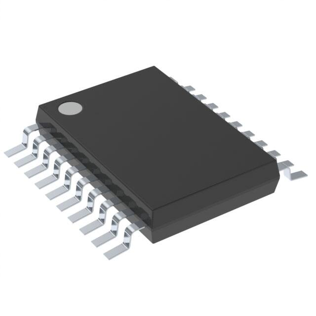
Device Information(1)
PART NUMBER
SN74LVCZ244A
PACKAGE
BODY SIZE (NOM)
SSOP (20)
7.50 mm x 5.30 mm
SOP (20)
12.60 mm x 5.30 mm
TSSOP (20)
6.50 mm x 4.40 mm
SOIC (20)
12.80 mm x 7.50 mm
(1) For all available packages, see the orderable addendum at
the end of the data sheet.
2 Applications
•
•
•
•
•
The SN74LVCZ244A device is organized as two 4-bit
line drivers with separate output-enable (OE) inputs.
When OE is low, the device passes data from the A
inputs to the Y outputs. When OE is high, the outputs
are in the high-impedance state.
Servers
Databases
Memory Systems
Network Switches
PCs and Notebooks
4 Simplified Schematic
1OE
2OE
1A1
1Y1
2A1
2Y1
1A2
1Y2
2A2
2Y2
1A3
1Y3
2A3
2Y3
1A4
1Y4
2A4
2Y4
1
An IMPORTANT NOTICE at the end of this data sheet addresses availability, warranty, changes, use in safety-critical applications,
intellectual property matters and other important disclaimers. PRODUCTION DATA.
�SN74LVCZ244A
SCES274I – MAY 1999 – REVISED OCTOBER 2014
www.ti.com
Table of Contents
1
2
3
4
5
6
7
8
Features ..................................................................
Applications ...........................................................
Description .............................................................
Simplified Schematic.............................................
Revision History.....................................................
Pin Configuration and Functions .........................
Specifications.........................................................
1
1
1
1
2
3
4
7.1
7.2
7.3
7.4
7.5
7.6
7.7
7.8
7.9
4
4
4
5
5
5
6
6
6
Absolute Maximum Ratings .....................................
Handling Ratings.......................................................
Recommended Operating Conditions ......................
Thermal Information ..................................................
Electrical Characteristics...........................................
Switching Characteristics, –40°C to 85°C.................
Switching Characteristics, –40°C to 125°C...............
Operating Characteristics..........................................
Typical Characteristics ..............................................
Parameter Measurement Information .................. 7
8.1 VCC = 2.7 V and 3.3 V ± 0.3 V .................................. 7
9
Detailed Description .............................................. 8
9.1
9.2
9.3
9.4
Overview ...................................................................
Functional Block Diagram .........................................
Feature Description...................................................
Device Functional Modes..........................................
8
8
8
8
10 Application and Implementation.......................... 9
10.1 Application Information............................................ 9
10.2 Typical Application ................................................. 9
11 Power Supply Recommendations ..................... 11
12 Layout................................................................... 11
12.1 Layout Guidelines ................................................. 11
12.2 Layout Example .................................................... 11
13 Device and Documentation Support ................. 12
13.1 Trademarks ........................................................... 12
13.2 Electrostatic Discharge Caution ............................ 12
13.3 Glossary ................................................................ 12
14 Mechanical, Packaging, and Orderable
Information ........................................................... 12
5 Revision History
Changes from Revision H (August 2003) to Revision I
Page
•
Updated document to new TI data sheet standards. ............................................................................................................. 1
•
Deleted Ordering Information table. ....................................................................................................................................... 1
•
Changed Ioff bullet in Features. .............................................................................................................................................. 1
•
Added Applications. ................................................................................................................................................................ 1
•
Added Pin Functions table...................................................................................................................................................... 3
•
Added Handling Ratings table. ............................................................................................................................................... 4
•
Changed Max operating temperature to 125°C in Recommended Operating Conditions table. .......................................... 4
•
Added Thermal Information table. .......................................................................................................................................... 5
•
Added –40°C TO 125°C temperature range to Electrical Characteristics table. .................................................................... 5
•
Added Switching Characteristics table for –40°C TO 125°C temperature range. .................................................................. 6
•
Added Typical Characteristics section.................................................................................................................................... 6
•
Added Detailed Description section........................................................................................................................................ 8
•
Added Application and Implementation section...................................................................................................................... 9
•
Added Power Supply Recommendations and Layout sections............................................................................................ 11
2
Submit Documentation Feedback
Copyright © 1999–2014, Texas Instruments Incorporated
Product Folder Links: SN74LVCZ244A
�SN74LVCZ244A
www.ti.com
SCES274I – MAY 1999 – REVISED OCTOBER 2014
6 Pin Configuration and Functions
DB, DW, N, NS, OR PW PACKAGE
(TOP VIEW)
1OE
1A1
2Y4
1A2
2Y3
1A3
2Y2
1A4
2Y1
GND
1
20
2
19
3
18
4
17
5
16
6
15
7
14
8
13
9
12
10
11
VCC
2OE
1Y1
2A4
1Y2
2A3
1Y3
2A2
1Y4
2A1
Pin Functions
PIN
NO.
NAME
I/O
DESCRIPTION
1
1OE
I
Output Enable 1
2
1A1
I
1A1 Input
3
2Y4
O
2Y4 Output
4
1A2
I
1A2 Input
5
2Y3
O
2Y3 Output
6
1A3
I
1A3 Input
7
2Y2
O
2Y2 Output
8
1A4
I
1A4 Input
9
2Y1
O
2Y1 Output
10
GND
—
Ground
11
2A1
I
2A1 Input
12
1Y4
O
1Y4 Output
13
2A2
I
2A2 Input
14
1Y3
O
1Y3 Output
15
2A3
I
2A3 Input
16
1Y2
O
1Y2 Output
17
2A4
I
2A4 Input
18
1Y1
O
1Y1 Output
19
2OE
I
Output Enable 2
20
VCC
—
Power Pin
Submit Documentation Feedback
Copyright © 1999–2014, Texas Instruments Incorporated
Product Folder Links: SN74LVCZ244A
3
�SN74LVCZ244A
SCES274I – MAY 1999 – REVISED OCTOBER 2014
www.ti.com
7 Specifications
7.1 Absolute Maximum Ratings
over operating free-air temperature range (unless otherwise noted) (1)
VCC
MIN
MAX
Supply voltage range
–0.5
6.5
UNIT
V
(2)
VI
Input voltage range
–0.5
6.5
V
VO
Voltage range applied to any output in the high-impedance or power-off state (2)
–0.5
6.5
V
VO
Voltage range applied to any output in the high or low state (2) (3)
–0.5
VCC + 0.5
V
IIK
Input clamp current
VI < 0
–50
mA
IOK
Output clamp current
VO < 0
–50
mA
IO
Continuous output current
±50
mA
±100
mA
Continuous current through VCC or GND
(1)
(2)
(3)
Stresses beyond those listed under Absolute Maximum Ratings may cause permanent damage to the device. These are stress ratings
only, and functional operation of the device at these or any other conditions beyond those indicated under Recommended Operating
Conditions is not implied. Exposure to absolute-maximum-rated conditions for extended periods may affect device reliability.
The input negative-voltage and output voltage ratings may be exceeded if the input and output current ratings are observed.
The value of VCC is provided in the Recommended Operating Conditions table.
7.2 Handling Ratings
Tstg
V(ESD)
(1)
(2)
MIN
MAX
UNIT
–65
150
°C
Human body model (HBM), per ANSI/ESDA/JEDEC JS-001, all
pins (1)
0
2500
Charged device model (CDM), per JEDEC specification
JESD22-C101, all pins (2)
0
4000
Storage temperature range
Electrostatic discharge
V
JEDEC document JEP155 states that 500-V HBM allows safe manufacturing with a standard ESD control process.
JEDEC document JEP157 states that 250-V CDM allows safe manufacturing with a standard ESD control process.
7.3 Recommended Operating Conditions
over operating free-air temperature range (unless otherwise noted) (1)
MIN
MAX
2.7
3.6
VCC
Supply voltage
VIH
High-level input voltage
VCC = 2.7 V to 3.6 V
VIL
Low-level input voltage
VCC = 2.7 V to 3.6 V
VI
Input voltage
VO
Output voltage
IOH
High-level output current
IOL
Low-level output current
Δt/Δv
Input transition rise or fall rate
Δt/ΔVCC
Power-up ramp rate
150
TA
Operating free-air temperature
–40
(1)
4
UNIT
V
2
V
0.8
V
0
5.5
V
High or low state
0
VCC
3-state
0
5.5
VCC = 2.7 V
–12
VCC = 3 V
–24
VCC = 2.7 V
12
VCC = 3 V
24
6
V
mA
mA
ns/V
µs/V
125
°C
All unused inputs of the device must be held at VCC or GND to ensure proper device operation. Refer to the TI application report,
Implications of Slow or Floating CMOS Inputs, (SCBA004).
Submit Documentation Feedback
Copyright © 1999–2014, Texas Instruments Incorporated
Product Folder Links: SN74LVCZ244A
�SN74LVCZ244A
www.ti.com
SCES274I – MAY 1999 – REVISED OCTOBER 2014
7.4 Thermal Information
SN74LVCZ244A
THERMAL METRIC (1)
DB
DW
NS
PW
UNIT
20 PINS
RθJA
97.7
78.7
77.9
103.5
RθJC(top) Junction-to-case (top) thermal resistance
59.4
45.0
44.5
37.9
RθJB
Junction-to-board thermal resistance
52.9
46.2
45.5
54.5
ψJT
Junction-to-top characterization parameter
21.4
18.3
18.3
3.3
ψJB
Junction-to-board characterization parameter
52.5
45.8
45.1
53.9
(1)
Junction-to-ambient thermal resistance
°C/W
For more information about traditional and new thermal metrics, see the IC Package Thermal Metrics application report (SPRA953).
7.5 Electrical Characteristics
over recommended operating free-air temperature range (unless otherwise noted)
PARAMET
ER
TEST CONDITIONS
IOH = –100 μA
VOH
VOL
II
–40°C TO 85°C
VCC
MIN TYP
2.7 V to 3.6 V
(1)
MAX
MIN
TYP
MAX
UNIT
VCC – 0.2
VCC – 0.2
2.7 V
2.2
2.2
3V
2.4
2.4
IOH = –24 mA
3V
2.2
IOL = 100 μA
2.7 V to 3.6 V
IOL = 12 mA
2.7 V
0.4
0.4
IOL = 24 mA
3V
0.55
0.55
3.6 V
±5
±5
μA
0
±5
±5
μA
IOH = –12 mA
VI = 0 to 5.5 V
Ioff
VI or VO = 5.5 V
IOZ
VO = 0 to 5.5 V
V
2.2
0.2
0.2
V
3.6 V
±5
±5
μA
IOZPU
VO = 0.5 to 2.5 V,
OE = don't care
0 to 1.5 V
±5
±5
μA
IOZPD
VO = 0.5 to 2.5 V,
OE = don't care
1.5 V to 0
±5
±5
μA
100
100
100
100
100
100
VI = VCC or GND
ICC
ΔICC
(1)
(2)
–40°C TO 125°C
3.6 V ≤ VI ≤ 5.5
V (2)
IO = 0
3.6 V
One input at VCC – 0.6 V, Other inputs
at VCC or GND
2.7 V to 3.6 V
μA
μA
Ci
VI = VCC or GND
3.3 V
3.5
—
pF
Co
VO = VCC or GND
3.3 V
5.5
—
pF
All typical values are at VCC = 3.3 V, TA = 25°C.
This applies in the disabled state only.
7.6 Switching Characteristics, –40°C to 85°C
over recommended operating free-air temperature range (unless otherwise noted) (see Figure 3)
PARAMETER
FROM
(INPUT)
TO
(OUTPUT)
tpd
A or B
ten
OE
tdis
OE
VCC = 2.7 V
MIN
VCC = 3.3 V ± 0.3 V
UNIT
MAX
MIN
MAX
B or A
6.9
1.5
5.9
ns
A or B
8.6
1.5
7.6
ns
A or B
6.8
1.5
6.5
ns
Submit Documentation Feedback
Copyright © 1999–2014, Texas Instruments Incorporated
Product Folder Links: SN74LVCZ244A
5
�SN74LVCZ244A
SCES274I – MAY 1999 – REVISED OCTOBER 2014
www.ti.com
7.7 Switching Characteristics, –40°C to 125°C
over recommended operating free-air temperature range (unless otherwise noted) (see Figure 3)
PARAMETER
FROM
(INPUT)
TO
(OUTPUT)
tpd
A or B
ten
tdis
VCC = 2.7 V
MIN
VCC = 3.3 V ± 0.3 V
UNIT
MAX
MIN
MAX
B or A
7.4
1.5
6.4
ns
OE
A or B
9.1
1.5
8.1
ns
OE
A or B
7.3
1.5
7.1
ns
7.8 Operating Characteristics
TA = 25°C
TEST
CONDITIONS
PARAMETER
Cpd
Outputs enabled
Power dissipation capacitance per buffer/driver
VCC = 3.3 V
40
f = 10 MHz
Outputs disabled
UNIT
TYP
pF
3
7.9 Typical Characteristics
6
4
3.5
5
4
2.5
TPD (ns)
TPD (ns)
3
2
1.5
3
2
1
1
0.5
TPD in ns
TPD in ns
0
-100
0
-50
0
50
Temperature (qC)
100
150
0
0.5
D001
Figure 1. TPD Across Temperature at 3.3 V
6
Submit Documentation Feedback
1
1.5
2
VCC (V)
2.5
3
3.5
D002
Figure 2. TPD Across VCC at 25°C
Copyright © 1999–2014, Texas Instruments Incorporated
Product Folder Links: SN74LVCZ244A
�SN74LVCZ244A
www.ti.com
SCES274I – MAY 1999 – REVISED OCTOBER 2014
8 Parameter Measurement Information
8.1 VCC = 2.7 V and 3.3 V ± 0.3 V
2 × VCC
S1
500 Ω
From Output
Under Test
GND
CL = 30 pF
(see Note A)
TEST
S1
tpd
tPLZ/tPZL
tPHZ/tPZH
Open
2 × VCC
GND
Open
500 Ω
tw
LOAD CIRCUIT
VCC
VCC
Timing
Input
Input
VCC/2
VCC/2
0V
VCC/2
0V
tsu
VOLTAGE WAVEFORMS
PULSE DURATION
th
VCC
Data
Input
VCC/2
VCC/2
0V
VOLTAGE WAVEFORMS
SETUP AND HOLD TIMES
VCC
Output
Control
(low-level
enabling)
VCC/2
VCC/2
0V
tPZL
VCC
Input
VCC/2
VCC/2
0V
tPLH
Output
Waveform 1
S1 at 2 × VCC
(see Note B)
tPHL
VCC/2
VCC
VCC/2
VOL + 0.3 V
VOL
tPZH
VOH
Output
tPLZ
VCC/2
VOL
tPHZ
Output
Waveform 2
S1 at GND
(see Note B)
VOLTAGE WAVEFORMS
PROPAGATION DELAY TIMES
VCC/2
VOH − 0.3 V
VOH
0V
VOLTAGE WAVEFORMS
ENABLE AND DISABLE TIMES
NOTES: A. CL includes probe and jig capacitance.
B. Waveform 1 is for an output with internal conditions such that the output is low, except when disabled by the output control.
Waveform 2 is for an output with internal conditions such that the output is high, except when disabled by the output control.
C. All input pulses are supplied by generators having the following characteristics: PRR≤ 10 MHz, ZO = 50 Ω, tr ≤ 2 ns, tf ≤ 2 ns.
D. The outputs are measured one at a time, with one transition per measurement.
E. t PLZ and t PHZ are the same as t dis.
F. t PZL and t PZH are the same as t en .
G. t PLH and t PHL are the same as t pd .
H. All parameters and waveforms are not applicable to all devices.
Figure 3. Load Circuit and Voltage Waveforms
Submit Documentation Feedback
Copyright © 1999–2014, Texas Instruments Incorporated
Product Folder Links: SN74LVCZ244A
7
�SN74LVCZ244A
SCES274I – MAY 1999 – REVISED OCTOBER 2014
www.ti.com
9 Detailed Description
9.1 Overview
This octal buffer/line driver is designed for 2.7-V to 3.6-V VCC operation.
The SN74LVCZ244A device is organized as two 4-bit line drivers with separate output-enable (OE) inputs. When
OE is low, the device passes data from the A inputs to the Y outputs. When OE is high, the outputs are in the
high-impedance state.
Inputs can be driven from either 3.3-V or 5-V devices. This feature allows the use of this device as a translator in
a mixed 3.3-V/5-V system environment.
When VCC is between 0 and 1.5 V, the device is in the high-impedance state during power up or power down.
However, to ensure the high-impedance state above 1.5 V, OE should be tied to VCC through a pullup resistor;
the minimum value of the resistor is determined by the current-sinking capability of the driver.
This device is fully specified for hot-insertion applications using Ioff and power-up 3-state. The Ioff circuitry disables
the outputs, preventing damaging current backflow through the device when it is powered down. The power-up 3state circuitry places the outputs in the high-impedance state during power up and power down, which prevents
driver conflict.
9.2 Functional Block Diagram
1OE
2OE
1A1
1Y1
2A1
2Y1
1A2
1Y2
2A2
2Y2
1A3
1Y3
2A3
2Y3
1A4
1Y4
2A4
2Y4
9.3 Feature Description
•
•
•
•
Wide operating voltage range
– Operates from 2.7 V to 3.6 V
Allows down-voltage translation
– Inputs accept voltages to 5.5 V
Ioff feature
– Allows voltages on the inputs and outputs when VCC is 0 V
Power-up 3-state feature
– Keeps the outputs in high impedance during power up and allows for hot insertion
9.4 Device Functional Modes
Table 1. Function Table
INPUTS
8
OE
A
OUTPUTS
Y
L
H
H
L
L
L
H
X
High-Z
Submit Documentation Feedback
Copyright © 1999–2014, Texas Instruments Incorporated
Product Folder Links: SN74LVCZ244A
�SN74LVCZ244A
www.ti.com
SCES274I – MAY 1999 – REVISED OCTOBER 2014
10 Application and Implementation
NOTE
Information in the following applications sections is not part of the TI component
specification, and TI does not warrant its accuracy or completeness. TI’s customers are
responsible for determining suitability of components for their purposes. Customers should
validate and test their design implementation to confirm system functionality.
10.1 Application Information
Inputs can be driven from either 3.3-V or 5-V devices. This feature allows the use of this device as a translator in
a mixed 3.3-V/5-V system environment.
The SN74LVCZ244A device is fully specified for partial-power-down applications using Ioff. The Ioff circuitry
disables the outputs, preventing damaging current backflow through the device when it is powered down. This
device is fully specified for hot-insertion applications using Ioff and power-up 3-state. The Ioff circuitry disables the
outputs, preventing damaging current backflow through the device when it is powered down.
The power-up 3-state circuitry places the outputs in the high-impedance state during power up and power down,
which prevents driver conflict. To ensure the high-impedance state during power up or power down, OE should
be tied to VCC through a pullup resistor; the minimum value of the resistor is determined by the current-sinking
capability of the driver.
10.2 Typical Application
Regulated 3.3 V
OE
A1
VCC
Y1
µC
System Logic
µC or
A4
Y4
LEDs
System Logic
GND
Figure 4. Typical Application Schematic
10.2.1 Design Requirements
This device uses CMOS technology and has balanced output drive. Care should be taken to avoid bus
contention, because it can drive currents that would exceed maximum limits. The high drive will also create fast
edges into light loads; therefore, routing and load conditions should be considered to prevent ringing.
Submit Documentation Feedback
Copyright © 1999–2014, Texas Instruments Incorporated
Product Folder Links: SN74LVCZ244A
9
�SN74LVCZ244A
SCES274I – MAY 1999 – REVISED OCTOBER 2014
www.ti.com
Typical Application (continued)
10.2.2 Detailed Design Procedure
1. Recommended Input Conditions:
– For rise time and fall time specifications, see Δt/ΔV in the Recommended Operating Conditions table.
– For specified high and low levels, see VIH and VIL in the Recommended Operating Conditions table.
– Inputs are overvoltage tolerant allowing them to go as high as 5.5 V at any valid VCC.
2. Recommend Output Conditions:
– Load currents should not exceed 50 mA per output and 100 mA total for the part.
– Outputs should not be pulled above VCC.
10.2.3 Application Curves
300
250
ICC (mA)
200
150
100
ICC 1.8 V
ICC 2.5 V
ICC 3.3 V
50
0
0
10
20
30
40
Frequency (MHz)
50
60
D001
Figure 5. ICC vs Frequency
10
Submit Documentation Feedback
Copyright © 1999–2014, Texas Instruments Incorporated
Product Folder Links: SN74LVCZ244A
�SN74LVCZ244A
www.ti.com
SCES274I – MAY 1999 – REVISED OCTOBER 2014
11 Power Supply Recommendations
The power supply can be any voltage between the MIN and MAX supply voltage rating located in the
Recommended Operating Conditions table.
Each VCC pin should have a good bypass capacitor to prevent power disturbance. For devices with a single
supply, 0.1 μF bypass capacitor is recommended. If there are multiple VCC pins, 0.01 μF or 0.022 μF is
recommended for each power pin. It is acceptable to parallel multiple bypass capacitors to reject different
frequencies of noise. A 0.1 μF and 1 μF are commonly used in parallel. The bypass capacitor should be installed
as close to the power pin as possible for best results.
12 Layout
12.1 Layout Guidelines
When using multiple bit logic devices, inputs should not float. In many cases, functions or parts of functions of
digital logic devices are unused. Some examples are when only two inputs of a triple-input AND gate are used,
or when only 3 of the 4-buffer gates are used. Such input pins should not be left unconnected because the
undefined voltages at the outside connections result in undefined operational states.
Specified in Figure 6 are rules that must be observed under all circumstances. All unused inputs of digital logic
devices must be connected to a high or low bias to prevent them from floating. The logic level that should be
applied to any particular unused input depends on the function of the device. Generally they will be tied to GND
or VCC, whichever makes more sense or is more convenient. It is acceptable to float outputs unless the part is a
transceiver. If the transceiver has an output enable pin, it will disable the outputs section of the part when
asserted. This will not disable the input section of the I/Os so they also cannot float when disabled.
12.2 Layout Example
Vcc
Unused Input
Input
Output
Unused Input
Output
Input
Figure 6. Layout Diagram
Submit Documentation Feedback
Copyright © 1999–2014, Texas Instruments Incorporated
Product Folder Links: SN74LVCZ244A
11
�SN74LVCZ244A
SCES274I – MAY 1999 – REVISED OCTOBER 2014
www.ti.com
13 Device and Documentation Support
13.1 Trademarks
All trademarks are the property of their respective owners.
13.2 Electrostatic Discharge Caution
These devices have limited built-in ESD protection. The leads should be shorted together or the device placed in conductive foam
during storage or handling to prevent electrostatic damage to the MOS gates.
13.3 Glossary
SLYZ022 — TI Glossary.
This glossary lists and explains terms, acronyms, and definitions.
14 Mechanical, Packaging, and Orderable Information
The following pages include mechanical, packaging, and orderable information. This information is the most
current data available for the designated devices. This data is subject to change without notice and revision of
this document. For browser-based versions of this data sheet, refer to the left-hand navigation.
12
Submit Documentation Feedback
Copyright © 1999–2014, Texas Instruments Incorporated
Product Folder Links: SN74LVCZ244A
�PACKAGE OPTION ADDENDUM
www.ti.com
10-Dec-2020
PACKAGING INFORMATION
Orderable Device
Status
(1)
Package Type Package Pins Package
Drawing
Qty
Eco Plan
(2)
Lead finish/
Ball material
MSL Peak Temp
Op Temp (°C)
Device Marking
(3)
(4/5)
(6)
SN74LVCZ244ADBR
ACTIVE
SSOP
DB
20
2000
RoHS & Green
NIPDAU
Level-1-260C-UNLIM
-40 to 125
CV244A
SN74LVCZ244ADWR
ACTIVE
SOIC
DW
20
2000
RoHS & Green
NIPDAU
Level-1-260C-UNLIM
-40 to 125
LVCZ244A
SN74LVCZ244ANSR
ACTIVE
SO
NS
20
2000
RoHS & Green
NIPDAU
Level-1-260C-UNLIM
-40 to 125
LVCZ244A
SN74LVCZ244APW
ACTIVE
TSSOP
PW
20
70
RoHS & Green
NIPDAU
Level-1-260C-UNLIM
-40 to 125
CV244A
SN74LVCZ244APWR
ACTIVE
TSSOP
PW
20
2000
RoHS & Green
NIPDAU
Level-1-260C-UNLIM
-40 to 125
CV244A
SN74LVCZ244APWT
ACTIVE
TSSOP
PW
20
250
RoHS & Green
NIPDAU
Level-1-260C-UNLIM
-40 to 125
CV244A
(1)
The marketing status values are defined as follows:
ACTIVE: Product device recommended for new designs.
LIFEBUY: TI has announced that the device will be discontinued, and a lifetime-buy period is in effect.
NRND: Not recommended for new designs. Device is in production to support existing customers, but TI does not recommend using this part in a new design.
PREVIEW: Device has been announced but is not in production. Samples may or may not be available.
OBSOLETE: TI has discontinued the production of the device.
(2)
RoHS: TI defines "RoHS" to mean semiconductor products that are compliant with the current EU RoHS requirements for all 10 RoHS substances, including the requirement that RoHS substance
do not exceed 0.1% by weight in homogeneous materials. Where designed to be soldered at high temperatures, "RoHS" products are suitable for use in specified lead-free processes. TI may
reference these types of products as "Pb-Free".
RoHS Exempt: TI defines "RoHS Exempt" to mean products that contain lead but are compliant with EU RoHS pursuant to a specific EU RoHS exemption.
Green: TI defines "Green" to mean the content of Chlorine (Cl) and Bromine (Br) based flame retardants meet JS709B low halogen requirements of


 工商网监
湘ICP备2023018690号
工商网监
湘ICP备2023018690号
