SN75C189, SN75C189A
QUADRUPLE LOW-POWER LINE RECEIVERS
SLLS041G – OCTOBER 1988 – REVISED JANUARY 2000
D
D
D
D
D
D
D
D
Meet or Exceed the Requirements of
TIA/EIA-232-F and ITU Recommendation
V.28
Low Supply Current . . . 420 µA Typ
Preset On-Chip Input Noise Filter
Built-in Input Hysteresis
Response and Threshold Control Inputs
Push-Pull Outputs
Functionally Interchangeable and
Pin-to-Pin Compatible With
Texas Instruments SN75189/SN75189A and
Motorola MC1489/MC1489A
Package Options Include Plastic
Small-Outline (D) and Shrink Small-Outline
(DB) Packages, and Standard Plastic (N)
DIP
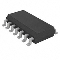
D, DB, OR N PACKAGE
(TOP VIEW)
1A
1 CONT
1Y
2A
2 CONT
2Y
GND
1
14
2
13
3
12
4
11
5
10
6
9
7
8
VCC
4A
4 CONT
4Y
3A
3 CONT
3Y
description
The SN75C189 and SN75C189A are low-power, bipolar, quadruple line receivers that are used to interface data
terminal equipment (DTE) with data circuit-terminating equipment (DCE). These devices have been designed
to conform to TIA/EIA-232-F.
The SN75C189 has a 0.33-V typical hysteresis, compared with 0.97 V for the SN75C189A. Each receiver has
provision for adjustment of the overall input threshold levels. This is achieved by choosing external series
resistors and voltages to provide bias levels for the response-control pins. The output is in the high logic state
if the input is open circuit or shorted to ground.
These devices have an on-chip filter that rejects input pulses of less than 1-µs duration. An external capacitor
can be connected from the control pins to ground to provide further input noise filtering for each receiver.
The SN75C189 and SN75C189A have been designed using low-power techniques in a bipolar technology. In
most applications, these receivers interface to single inputs of peripheral devices such as UARTs, ACEs, or
microprocessors. By using sampling, such peripheral devices usually are insensitive to the transition times of
the input signals. If this is not the case, or for other uses, it is recommended that the SN75C189 and SN75C189A
outputs be buffered by single Schmitt input gates or single gates of the HCMOS, ALS, or 74F logic families.
The SN75C189 and SN75C189A are characterized for operation from 0°C to 70°C.
Please be aware that an important notice concerning availability, standard warranty, and use in critical applications of
Texas Instruments semiconductor products and disclaimers thereto appears at the end of this data sheet.
Copyright 2000, Texas Instruments Incorporated
PRODUCTION DATA information is current as of publication date.
Products conform to specifications per the terms of Texas Instruments
standard warranty. Production processing does not necessarily include
testing of all parameters.
POST OFFICE BOX 655303
• DALLAS, TEXAS 75265
1
�SN75C189, SN75C189A
QUADRUPLE LOW-POWER LINE RECEIVERS
SLLS041G – OCTOBER 1988 – REVISED JANUARY 2000
logic symbol†
1A
1 CONT
2A
2 CONT
3A
3 CONT
4A
4 CONT
logic diagram (each receiver)
1
A
2
Response
Control
3
THRESHOLD
ADJUST
4
5
6
10
8
9
1Y
Y
2Y
3Y
13
11
12
4Y
† This symbol is in accordance with ANSI/IEEE Std 91-1984 and
IEC Publication 617-12.
schematic of inputs and outputs
EQUIVALENT OF EACH INPUT‡
EQUIVALENT OF EACH OUTPUT
VCC
Input
ESD
Protection
3.4 kΩ
ESD
Protection
Response
Control
Output
1.5 kΩ
530 Ω
‡ All resistor values shown are nominal.
absolute maximum ratings over operating free-air temperature range (unless otherwise noted)§
Supply voltage, VCC (see Note 1) . . . . . . . . . . . . . . . . . . . . . . . . . . . . . . . . . . . . . . . . . . . . . . . . . . . . . . . . . . . . . 7 V
Input voltage range, VI . . . . . . . . . . . . . . . . . . . . . . . . . . . . . . . . . . . . . . . . . . . . . . . . . . . . . . . . . . . . . . –30 V to 30 V
Output voltage range, VO . . . . . . . . . . . . . . . . . . . . . . . . . . . . . . . . . . . . . . . . . . . . . . . . . . . . –0.3 V to VCC+ 0.3 V
Package thermal impedance, θJA (see Note 2): D package . . . . . . . . . . . . . . . . . . . . . . . . . . . . . . . . . . . 86°C/W
DB package . . . . . . . . . . . . . . . . . . . . . . . . . . . . . . . . . 96°C/W
N package . . . . . . . . . . . . . . . . . . . . . . . . . . . . . . . . . . . 80°C/W
Lead temperature 1,6 mm (1/16 inch) from case for 10 seconds . . . . . . . . . . . . . . . . . . . . . . . . . . . . . . . 260°C
Storage temperature range, Tstg . . . . . . . . . . . . . . . . . . . . . . . . . . . . . . . . . . . . . . . . . . . . . . . . . . . –65°C to 150°C
§ Stresses beyond those listed under “absolute maximum ratings” may cause permanent damage to the device. These are stress ratings only, and
functional operation of the device at these or any other conditions beyond those indicated under “recommended operating conditions” is not
implied. Exposure to absolute-maximum-rated conditions for extended periods may affect device reliability.
NOTES: 1. All voltages are with respect to network GND.
2. The package thermal impedance is calculated in accordance with JESD 51.
2
POST OFFICE BOX 655303
• DALLAS, TEXAS 75265
�SN75C189, SN75C189A
QUADRUPLE LOW-POWER LINE RECEIVERS
SLLS041G – OCTOBER 1988 – REVISED JANUARY 2000
recommended operating conditions
MIN
NOM
MAX
VCC
VI
Supply voltage
4.5
5
6
Input voltage (see Note 3)
–25
IOH
IOL
High-level output current
–3.2
mA
Low-level output current
3.2
mA
Response-control current
±1
mA
25
UNIT
V
V
TA
Operating free-air temperature
0
70
°C
NOTE 3: The algebraic convention, where the more positive (less negative) limit is designated as maximum, is used in this data sheet for logic
levels only, e.g., if –10 V is a maximum, the typical value is a more negative voltage.
electrical characteristics over recommended free-air temperature range, VCC = 5 V ±10% (unless
otherwise noted) (see Note 4)
PARAMETER
VIT
IT+
Positive going input threshold voltage
Positive-going
VIT
IT–
Negative going input threshold voltage
Negative-going
Vh
hys
Input hysteresis voltage (VIT
IT+ – VIT
IT–)
VOH
TEST CONDITIONS
’C189
’C189A
’C189
’C189A
’C189
’C189A
High level output voltage
High-level
See Figure 1
MIN
TYP†
1
1.5
1.6
2.25
0.75
See Figure 1
See Figure 1
MAX
1.25
0.75
1
0.15
0.33
0.65
0.97
VCC = 4.5 V to 6 V,,
IOH = –20 µA
VI = 0.75 V,,
35
3.5
VCC = 4.5 V to 6 V,
IOH = –3.2 mA
VI = 0.75 V,
2.5
VI = 3 V,,
1.25
UNIT
V
V
V
V
VOL
Low level output voltage
Low-level
VCC = 4.5 V to 6 V,,
IOL = 3.2 mA
IIH
High level input current
High-level
See Figure 2
VI = 25 V
VI = 3 V
3.6
8.3
0.43
1
IIL
Low level input current
Low-level
See Figure 2
VI = –25 V
VI = –3 V
–3.6
–8.3
–0.43
–1
IOS
Short-circuit output current
See Figure 3
ICC
Supply current
VI = 5 V,
See Figure 2
04
0.4
No load,
V
mA
mA
–35
mA
420
700
µA
TYP
MAX
UNIT
† All typical values are at TA = 25°C.
NOTE 4: All characteristics are measured with response-control terminal open.
switching characteristics, VCC = 5 V ±10%, TA = 25°C
PARAMETER
tPLH
tPHL
tTLH
tTHL
TEST CONDITIONS
MIN
Propagation delay time, low- to high-level output
6
µs
Propagation delay time, high- to low-level output
Transition time, low- to high-level output‡
6
µs
500
ns
300
ns
RL = 5 kΩ,
CL = 50 pF,
Transition time, high- to low-level output‡
See Figure 4
tw(N)
Duration of longest pulse rejected as noise§
1
6
µs
‡ Measured between 10% and 90% points of output waveform
§ The receiver ignores any positive- or negative-going pulse that is less than the minimum value of tw(N) and accepts any postive- or negative-going
pulse greater than the maximum of tw(N).
POST OFFICE BOX 655303
• DALLAS, TEXAS 75265
3
�SN75C189, SN75C189A
QUADRUPLE LOW-POWER LINE RECEIVERS
SLLS041G – OCTOBER 1988 – REVISED JANUARY 2000
PARAMETER MEASUREMENT INFORMATION
VCC
ÎÎÎ
ÎÎ ÎÎÎ
ÎÎ
VIT, V1
VOH
Response
Control
Open Unless
Otherwise Specified
VOL
IOL
RC
RC
CC
VC
–VC
NOTE A: Arrows indicate actual direction of current flow. Current into a terminal is a positive value.
Figure 1. VT+, VIT–, VOH, VOL
VCC
VI
ICC
IIH
Open
–IIL
Response Control
Open
NOTE A: Arrows indicate actual direction of current flow. Current into a terminal is a positive value.
Figure 2. IIH, IIL, ICC
VCC
–IOS
Response Control
Open
NOTE A: Arrows indicate actual direction of current flow. Current into a terminal is a positive value.
Figure 3. IOS
4
POST OFFICE BOX 655303
• DALLAS, TEXAS 75265
–IOH
�SN75C189, SN75C189A
QUADRUPLE LOW-POWER LINE RECEIVERS
SLLS041G – OCTOBER 1988 – REVISED JANUARY 2000
PARAMETER MEASUREMENT INFORMATION
VCC
Pulse
Generator
(see Note B)
Output
RL = 5 kΩ
Response Control
Open
CL = 50 pF
(see Note A)
TEST CIRCUIT
3V
1.5 V
Input
1.5 V
0V
tPLH
tPHL
90%
Output
90%
1.5 V
10%
1.5 V
10%
tTHL
VOH
VOL
tTLH
VOLTAGE WAVEFORMS
NOTES: A. CL includes probe and jig capacitances.
B. The pulse generator has the following characteristics: ZO = 50 Ω, tw = 25 µs.
Figure 4. Test Circuit and Voltage Waveforms
POST OFFICE BOX 655303
• DALLAS, TEXAS 75265
5
�SN75C189, SN75C189A
QUADRUPLE LOW-POWER LINE RECEIVERS
SLLS041G – OCTOBER 1988 – REVISED JANUARY 2000
TYPICAL CHARACTERISTICS
SN75C189
INPUT THRESHOLD VOLTAGE (POSITIVE GOING)
vs
FREE-AIR TEMPERATURE
SN75C189A
INPUT THRESHOLD VOLTAGE (POSITIVE GOING)
vs
FREE-AIR TEMPERATURE
2.4
1.5
VCC = 5.5 V
V IT+ – Input Threshold Voltage – V
V IT+ – Input Threshold Voltage – V
VCC = 5.5 V
1.4
1.3
1.2
2.2
2
1.8
1.6
1.4
1.2
1.1
0
20
40
60
80
0
100
20
Figure 5
80
100
SN75C189A
INPUT THRESHOLD VOLTAGE (NEGATIVE GOING)
vs
FREE-AIR TEMPERATURE
1.2
1.15
VCC = 5.5 V
VCC = 5.5 V
V IT– – Input Threshold Voltage – V
V IT– – Input Threshold Voltage – V
60
Figure 6
SN75C189
INPUT THRESHOLD VOLTAGE (NEGATIVE GOING)
vs
FREE-AIR TEMPERATURE
1.1
1
0.9
1.1
1.05
1
0.95
0.9
0.85
0.8
0
20
40
60
80
100
0
TA – Free-Air Temperature – °C
20
40
Figure 8
POST OFFICE BOX 655303
60
80
TA – Free-Air Temperature – °C
Figure 7
6
40
TA – Free-Air Temperature – °C
TA – Free-Air Temperature – °C
• DALLAS, TEXAS 75265
100
�SN75C189, SN75C189A
QUADRUPLE LOW-POWER LINE RECEIVERS
SLLS041G – OCTOBER 1988 – REVISED JANUARY 2000
TYPICAL CHARACTERISTICS
SN75C189A
INPUT HYSTERESIS
vs
FREE-AIR TEMPERATURE
SN75C189
INPUT HYSTERESIS
vs
FREE-AIR TEMPERATURE
1.2
0.40
0.38
1.1
0.36
Vhys – Input Hysteresis – V
Vhys – Input Hysteresis – V
VCC = 5 V
VCC = 5 V
0.34
0.32
0.30
0.28
0.26
1
0.9
0.8
0.7
0.6
0.24
0.5
0.22
0.20
0.4
0
20
40
60
80
100
120
0
20
TA – Free-Air Temperature – °C
VOL – Low-Level Output Voltage – V
VOH – High-Level Output Voltage – V
3.8
VCC = 4.5 V
IOH = –3.2 mA
VI = 0.75 V
3.4
3.2
3
2.8
2.6
2.4
2.2
40
100
LOW-LEVEL OUTPUT VOLTAGE
vs
FREE-AIR TEMPERATURE
3.8
20
80
Figure 10
HIGH-LEVEL OUTPUT VOLTAGE
vs
FREE-AIR TEMPERATURE
0
60
TA – Free-Air Temperature – °C
Figure 9
3.6
40
60
80
100
VCC = 4.5 V
IOH = –3.2 mA
VI = 3 V
3.6
3.4
3.2
3
2.8
2.6
2.4
2.2
0
TA – Free-Air Temperature – °C
20
40
60
80
100
TA – Free-Air Temperature – °C
Figure 11
Figure 12
POST OFFICE BOX 655303
• DALLAS, TEXAS 75265
7
�SN75C189, SN75C189A
QUADRUPLE LOW-POWER LINE RECEIVERS
SLLS041G – OCTOBER 1988 – REVISED JANUARY 2000
TYPICAL CHARACTERISTICS
SN75C189
HIGH-LEVEL INPUT CURRENT
vs
FREE-AIR TEMPERATURE
SN75C189A
HIGH-LEVEL INPUT CURRENT
vs
FREE-AIR TEMPERATURE
0.65
VCC = 4.5 V
VI = 3 V
I IH – High-Level Input Current – mA
I IH – High-Level Input Current – mA
0.7
0.65
0.6
0.55
0.5
0.45
VCC = 4.5 V
VI = 3 V
0.6
0.55
0.5
0.45
0.4
0.35
0.4
0
20
40
60
80
100
0
20
TA – Free-Air Temperature – °C
80
100
Figure 14
SN75C189
LOW-LEVEL INPUT CURRENT
vs
FREE-AIR TEMPERATURE
SN75C189A
LOW-LEVEL INPUT CURRENT
vs
FREE-AIR TEMPERATURE
–0.2
–0.2
VCC = 4.5 V
VI = 3 V
I IL – Low-Level Input Current – mA
VCC = 4.5 V
VI = 3 V
I IL – Low-Level Input Current – mA
60
TA – Free-Air Temperature – °C
Figure 13
–0.3
–0.4
–0.5
–0.6
–0.7
–0.3
–0.4
–0.5
–0.6
–0.7
–0.8
–0.8
0
20
40
60
80
100
0
20
40
Figure 15
Figure 16
POST OFFICE BOX 655303
60
80
TA – Free-Air Temperature – °C
TA – Free-Air Temperature – °C
8
40
• DALLAS, TEXAS 75265
100
�SN75C189, SN75C189A
QUADRUPLE LOW-POWER LINE RECEIVERS
SLLS041G – OCTOBER 1988 – REVISED JANUARY 2000
HIGH-LEVEL SHORT-CIRCUIT OUTPUT CURRENT
vs
FREE-AIR TEMPERATURE
0
VCC = 5.5 V
VO = 0
–2
–4
–6
–8
–10
–12
–14
–16
0
20
40
60
80
100
I OS(L) – Low-Level Short-Circuit Output Current – mA
IOS(H) – High-Level Short-Circuit Output Current – mA
TYPICAL CHARACTERISTICS
LOW-LEVEL SHORT-CIRCUIT OUTPUT CURRENT
vs
FREE-AIR TEMPERATURE
30
VCC = 5.5 V
VI = 0
25
20
15
10
5
0
0
20
TA – Free-Air Temperature – °C
SUPPLY CURRENT
vs
FREE-AIR TEMPERATURE
800
VCC = 5.5 V
VI = 5 V
I CC – Supply Current – µA
600
500
400
300
200
100
0
0
20
40
60
80
100
Figure 18
60
80
100
TA – Free-Air Temperature – °C
t PLH – Propagation Delay Time, Low-to-High Level Output – µ s
Figure 17
700
40
TA – Free-Air Temperature – °C
PROPAGATION DELAY TIME,
LOW- TO HIGH-LEVEL OUTPUT
vs
FREE-AIR TEMPERATURE
5
VCC = 4.5 V
CL = 50 pF
4.5
4
3.5
3
2.5
2
0
Figure 19
20
40
60
80
100
TA – Free-Air Temperature – °C
Figure 20
POST OFFICE BOX 655303
• DALLAS, TEXAS 75265
9
�SN75C189, SN75C189A
QUADRUPLE LOW-POWER LINE RECEIVERS
SLLS041G – OCTOBER 1988 – REVISED JANUARY 2000
PROPAGATION DELAY TIME,
HIGH- TO LOW-LEVEL OUTPUT
vs
FREE-AIR TEMPERATURE
t TLH – Transition Time, Low-to-High Level Output – µ s
t PHL – Propagation Delay Time, High-to-Low Level Output – µ s
TYPICAL CHARACTERISTICS
4
VCC = 4.5 V
CL = 50 pF
3.9
3.8
3.7
3.6
3.5
3.4
3.3
3.2
0
20
40
60
80
100
TA – Free-Air Temperature – °C
TRANSITION TIME,
LOW- TO HIGH-LEVEL OUTPUT
vs
FREE-AIR TEMPERATURE
400
VCC = 4.5 V
CL = 50 pF
350
300
250
200
150
100
0
20
t THL – Transition Time, High-to-Low Level Output – µ s
Figure 22
TRANSITION TIME,
HIGH- TO LOW-LEVEL OUTPUT
vs
FREE-AIR TEMPERATURE
200
VCC = 4.5 V
CL = 50 pF
180
160
140
120
100
80
60
40
0
20
40
60
80
TA – Free-Air Temperature – °C
Figure 23
POST OFFICE BOX 655303
60
80
TA – Free-Air Temperature – °C
Figure 21
10
40
• DALLAS, TEXAS 75265
100
100
�PACKAGE OPTION ADDENDUM
www.ti.com
14-Aug-2021
PACKAGING INFORMATION
Orderable Device
Status
(1)
Package Type Package Pins Package
Drawing
Qty
Eco Plan
(2)
Lead finish/
Ball material
MSL Peak Temp
Op Temp (°C)
Device Marking
(3)
(4/5)
(6)
SN75C189AD
ACTIVE
SOIC
D
14
50
RoHS & Green
NIPDAU
Level-1-260C-UNLIM
0 to 70
75C189A
SN75C189ADBR
ACTIVE
SSOP
DB
14
2000
RoHS & Green
NIPDAU
Level-1-260C-UNLIM
0 to 70
CA189A
SN75C189ADBRE4
ACTIVE
SSOP
DB
14
2000
RoHS & Green
NIPDAU
Level-1-260C-UNLIM
0 to 70
CA189A
SN75C189ADR
ACTIVE
SOIC
D
14
2500
RoHS & Green
NIPDAU
Level-1-260C-UNLIM
0 to 70
75C189A
SN75C189AN
ACTIVE
PDIP
N
14
25
RoHS & Green
NIPDAU
N / A for Pkg Type
0 to 70
SN75C189AN
SN75C189ANE4
ACTIVE
PDIP
N
14
25
RoHS & Green
NIPDAU
N / A for Pkg Type
0 to 70
SN75C189AN
SN75C189ANSR
ACTIVE
SO
NS
14
2000
RoHS & Green
NIPDAU
Level-1-260C-UNLIM
0 to 70
75C189A
SN75C189D
ACTIVE
SOIC
D
14
50
RoHS & Green
NIPDAU
Level-1-260C-UNLIM
0 to 70
SN75C189
SN75C189DR
ACTIVE
SOIC
D
14
2500
RoHS & Green
NIPDAU
Level-1-260C-UNLIM
0 to 70
SN75C189
SN75C189DRE4
ACTIVE
SOIC
D
14
2500
RoHS & Green
NIPDAU
Level-1-260C-UNLIM
0 to 70
SN75C189
SN75C189N
ACTIVE
PDIP
N
14
25
RoHS & Green
NIPDAU
N / A for Pkg Type
0 to 70
SN75C189N
SN75C189NSR
ACTIVE
SO
NS
14
2000
RoHS & Green
NIPDAU
Level-1-260C-UNLIM
0 to 70
75C189
(1)
The marketing status values are defined as follows:
ACTIVE: Product device recommended for new designs.
LIFEBUY: TI has announced that the device will be discontinued, and a lifetime-buy period is in effect.
NRND: Not recommended for new designs. Device is in production to support existing customers, but TI does not recommend using this part in a new design.
PREVIEW: Device has been announced but is not in production. Samples may or may not be available.
OBSOLETE: TI has discontinued the production of the device.
(2)
RoHS: TI defines "RoHS" to mean semiconductor products that are compliant with the current EU RoHS requirements for all 10 RoHS substances, including the requirement that RoHS substance
do not exceed 0.1% by weight in homogeneous materials. Where designed to be soldered at high temperatures, "RoHS" products are suitable for use in specified lead-free processes. TI may
reference these types of products as "Pb-Free".
RoHS Exempt: TI defines "RoHS Exempt" to mean products that contain lead but are compliant with EU RoHS pursuant to a specific EU RoHS exemption.
Green: TI defines "Green" to mean the content of Chlorine (Cl) and Bromine (Br) based flame retardants meet JS709B low halogen requirements of


 工商网监
湘ICP备2023018690号
工商网监
湘ICP备2023018690号
