Product
Folder
Sample &
Buy
Support &
Community
Tools &
Software
Technical
Documents
SN75LVDS83A
SLLS980E – JUNE 2009 – REVISED NOVEMBER 2016
SN75LVDS83A Flatlink™ Transmitter
1 Features
3 Description
•
The SN75LVDS83A Flatlink™ transmitter device
contains four 7-bit parallel-load serial-out shift
registers, a 7× clock synthesizer, and five LowVoltage Differential Signaling (LVDS) line drivers in a
single integrated circuit. These functions allow 28 bits
of single-ended LVTTL data to be synchronously
transmitted over five balanced-pair conductors for
receipt by a compatible receiver, such as the
SN75LVDS82 and LCD panels with integrated LVDS
receiver.
1
•
•
•
•
•
•
•
•
•
•
•
•
LVDS Display SerDes Interfaces Directly to LCD
Display Panels with Integrated LVDS
Package Options: 8.1 mm × 14 mm TSSOP
3.3-V Tolerant Data Inputs
Transfer Rate up to 100 Mpps (Mega Pixel Per
Second)
Pixel Clock Frequency Range: 10 MHz to 100
MHz
Suited for Display Resolutions Ranging From
HVGA up to HD With Low EMI
Operates From a Single 3.3-V Supply and
170 mW (Typical) at 75 MHz
28 Data Channels Plus Clock In Low-Voltage TTL
to 4 Data Channels Plus Clock Out Low-Voltage
Differential
Consumes Less Than 1 mW When Disabled
Selectable Rising or Falling Clock Edge Triggered
Inputs
ESD: 5000 V HBM
Support Spread Spectrum Clocking (SSC)
Compatible With all OMAP™ 2x, OMAP™ 3x, and
DaVinci™ Application Processors
When transmitting, data bits D0 through D27 are
each loaded into registers upon the edge of the input
clock signal (CLKIN). The rising or falling edge of the
clock can be selected via the clock select (CLKSEL)
pin. The frequency of CLKIN is multiplied seven
times, and then used to unload the data registers in
7-bit slices and serially. The four serial streams and a
phase-locked clock (CLKOUT) are then output to
LVDS output drivers. The frequency of CLKOUT is
the same as the input clock, CLKIN.
Device Information(1)
PART NUMBER
SN75LVDS83A
PACKAGE
TSSOP (56)
BODY SIZE (NOM)
14.00 mm × 6.10 mm
(1) For all available packages, see the orderable addendum at
the end of the data sheet.
2 Applications
•
•
•
•
•
Tablets
Industrial PC, Laptop, and Other Factory
Automation Displays
Patient Monitor and Medical Equipment Displays
Electronic Point-of-Sale (EPOS) Displays
Printer Displays
LVDS Application
swiv
Application
processor
TM
(e.g. OMAP )
el
SN75LVDS83A
TM
FlatLink Transmitter
TSSOP: 8 x 14mm DGG
1
An IMPORTANT NOTICE at the end of this data sheet addresses availability, warranty, changes, use in safety-critical applications,
intellectual property matters and other important disclaimers. PRODUCTION DATA.
�SN75LVDS83A
SLLS980E – JUNE 2009 – REVISED NOVEMBER 2016
www.ti.com
Table of Contents
1
2
3
4
5
6
7
Features ..................................................................
Applications ...........................................................
Description .............................................................
Revision History.....................................................
Description (continued).........................................
Pin Configuration and Functions .........................
Specifications.........................................................
7.1
7.2
7.3
7.4
7.5
7.6
7.7
7.8
7.9
8
9
1
1
1
2
3
3
6
Absolute Maximum Ratings ..................................... 6
ESD Ratings.............................................................. 6
Recommended Operating Conditions....................... 6
Thermal Information .................................................. 6
Electrical Characteristics........................................... 7
Dissipation Ratings ................................................... 7
Timing Requirements ................................................ 8
Switching Characteristics .......................................... 8
Typical Characteristics ............................................ 10
Parameter Measurement Information ................ 11
Detailed Description ............................................ 14
9.1
9.2
9.3
9.4
Overview .................................................................
Functional Block Diagram .......................................
Feature Description.................................................
Device Functional Modes........................................
14
14
15
16
10 Application and Implementation........................ 17
10.1 Application Information.......................................... 17
10.2 Typical Application ................................................ 23
11 Power Supply Recommendations ..................... 27
12 Layout................................................................... 27
12.1 Layout Guidelines ................................................. 27
12.2 Layout Example .................................................... 29
13 Device and Documentation Support ................. 31
13.1
13.2
13.3
13.4
13.5
Receiving Notification of Documentation Updates
Community Resources..........................................
Trademarks ...........................................................
Electrostatic Discharge Caution ............................
Glossary ................................................................
31
31
31
31
31
14 Mechanical, Packaging, and Orderable
Information ........................................................... 31
4 Revision History
NOTE: Page numbers for previous revisions may differ from page numbers in the current version.
Changes from Revision D (June 2011) to Revision E
Page
•
Added ESD Ratings table, Feature Description section, Device Functional Modes, Application and Implementation
section, Power Supply Recommendations section, Layout section, Device and Documentation Support section, and
Mechanical, Packaging, and Orderable Information section. ................................................................................................. 1
•
Deleted Ordering Information table; see POA at the end of the data sheet........................................................................... 1
•
Added Thermal Information table ........................................................................................................................................... 6
Changes from Revision C (August 2009) to Revision D
•
Changed 24-Bit Color Host to 24-bit LCD Panel Application Schematic From: G7(LSB) To: G7(MSB) ............................. 18
Changes from Revision B (July 2009) to Revision C
•
Page
Deleted sentence in the Pin Functions table for entry D0 - D27 - "supports 1.8V to 3.3V input voltage selectable by
VDD supply." .......................................................................................................................................................................... 4
Changes from Revision A (June 2009) to Revision B
•
Page
Page
Changed the data sheet From: Product Preview To: Production........................................................................................... 1
Changes from Original (June 2009) to Revision A
Page
•
Changed Description text From: Alternative device option: The SN75LVDS83A is an alternative... To: Alternative
device option: The SN75LVDS83B is an alternative... ........................................................................................................... 3
•
Changed Typical PRBS Output Signal vs Over One Clock Period graph............................................................................ 10
2
Submit Documentation Feedback
Copyright © 2009–2016, Texas Instruments Incorporated
Product Folder Links: SN75LVDS83A
�SN75LVDS83A
www.ti.com
SLLS980E – JUNE 2009 – REVISED NOVEMBER 2016
5 Description (continued)
The SN75LVDS83A requires no external components and little or no control. The data bus appears the same at
the input to the transmitter and output of the receiver with the data transmission transparent to the user(s). The
only user intervention is selecting a clock rising edge by inputting a high level to CLKSEL or a falling edge with a
low-level input, and the possible use of the Shutdown/Clear (SHTDN). SHTDN is an active-low input to inhibit the
clock, and shut off the LVDS output drivers for lower power consumption. A low-level on this signal clears all
internal registers to a low-level.
The SN75LVDS83A is characterized for operation over ambient air temperatures of –10°C to 70°C.
Alternative device option: The SN75LVDS83B is an alternative to the SN75LVDS83A for clock frequency range
of 10 MHz to 135 MHz. The SN75LVDS83B is available in a smaller BGA package in addition to the TSSOP
package.
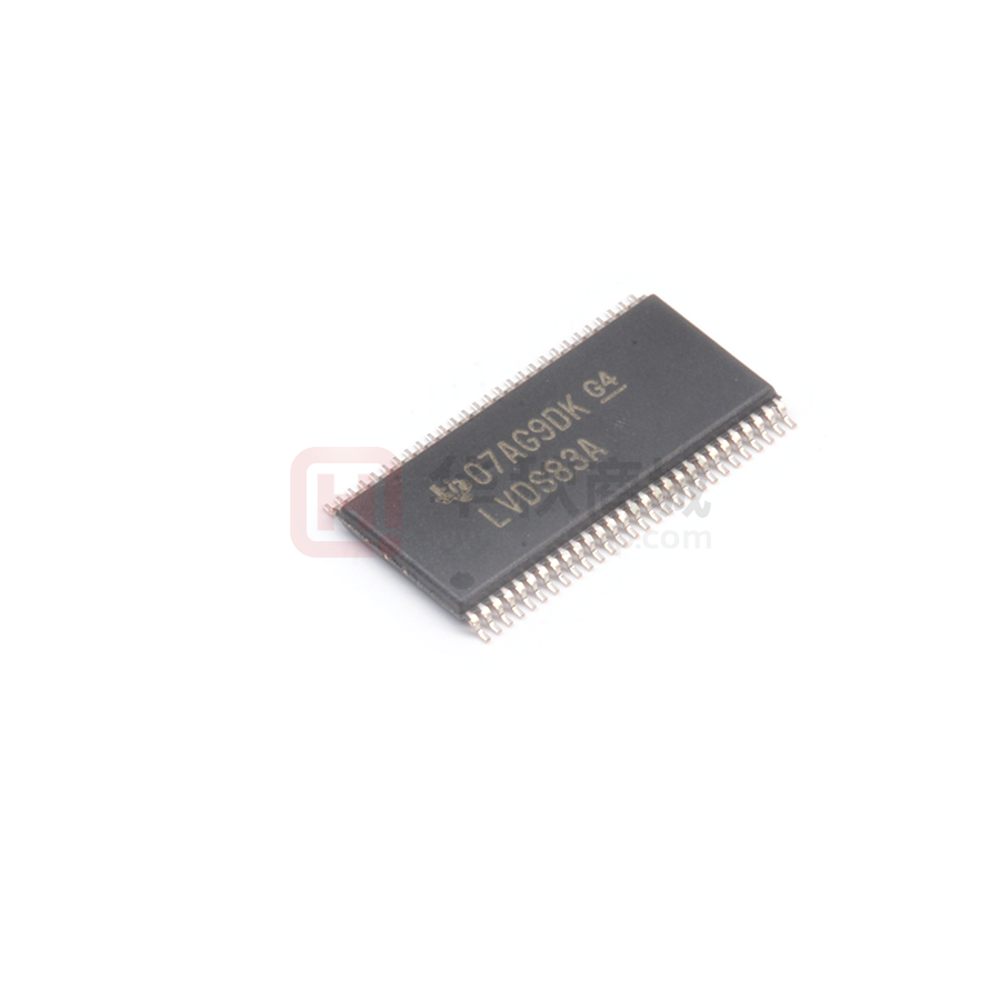
6 Pin Configuration and Functions
DGG Package
56-Pin TSSOP
Top View
VCC
1
56
D5
2
3
55
54
D7
GND
D8
4
53
5
52
GND
D1
6
51
D0
D9
D10
7
50
8
49
D27
GND
VCC
D11
9
10
48
47
D12
11
46
D13
12
45
Y1P
GND
D14
13
44
14
15
43
42
LVDSVCC
GND
Y2M
16
41
17
18
40
39
19
38
D19
GND
20
37
CLKOUTP
Y3M
Y3P
21
36
GND
D20
35
34
GND
D21
22
23
D22
24
33
D23
25
32
VCC
D24
D25
26
31
27
30
28
29
D6
D15
D16
CLKSEL
D17
D18
D4
D3
D2
Y0M
Y0P
Y1M
Y2P
CLKOUTM
PLLVCC
GND
SHTDN
CLKIN
D26
GND
Submit Documentation Feedback
Copyright © 2009–2016, Texas Instruments Incorporated
Product Folder Links: SN75LVDS83A
3
�SN75LVDS83A
SLLS980E – JUNE 2009 – REVISED NOVEMBER 2016
www.ti.com
Pin Functions
PIN
TYPE (1)
DESCRIPTION
NAME
NO.
CLKIN
31
I
CLKOUTM
40
O
CLKOUTP
39
O
CLKSEL
17
I
D0
51
I
D1
52
I
D2
54
I
D3
55
I
D4
56
I
D5
2
I
D6
3
I
D7
4
I
D8
6
I
D9
7
I
D10
8
I
D11
10
I
D12
11
I
D13
12
I
D14
14
I
D15
15
I
D16
16
I
D17
18
I
D18
19
I
D19
20
I
D20
22
I
D21
23
I
D22
24
I
D23
25
I
D24
27
I
D25
28
I
D26
30
I
D27
50
I
GND
5, 23, 21, 29,
43, 49, 53
P
Supply ground for VCC, LVDSVCC, and PLLVCC (2)
LVDSVCC
44
P
3.3-V LVDS output analog supply (2)
PLLVCC
34
P
3.3-V PLL analog supply (2)
SHTDN
32
I
CMOS with pulldown; device shut down; pull low (deassert) to shut down the device (low
power, resets all registers) and high (assert) for normal operation.
VCC
1, 9, 26
P
3.3-V digital supply voltage (2)
Y0M
48
O
Differential LVDS data outputs. Output is high-impedance when SHTDN is pulled low
(deasserted).
Y0P
47
O
Differential LVDS data outputs. Output is high-impedance when SHTDN is pulled low
(deasserted).
(1)
(2)
4
CMOS with pulldown; input pixel clock; rising or falling clock polarity is selectable by
Control input CLKSEL.
Differential LVDS pixel clock output.
Output is high-impedance when SHTDN is pulled low (de-asserted).
CMOS with pulldown; selects between rising edge input clock trigger (CLKSEL = VIH)
and falling edge input clock trigger (CLKSEL = VIL).
CMOS with pulldown; data inputs. To connect a graphic source successfully to a display,
the bit assignment of D[27:0] is critical (and not necessarily intuitive).
For input bit assignment, see Figure 14 to Figure 17 for details.
Note: if application only requires 18-bit color, connect unused inputs D5, D10, D11, D16,
D17, D23, and D27 to GND.
I = Input, O = Output, P = Power
For a multi-layer PCB, TI recommends keeping one common GND layer underneath the device and connecting all ground terminals
directly to this plane.
Submit Documentation Feedback
Copyright © 2009–2016, Texas Instruments Incorporated
Product Folder Links: SN75LVDS83A
�SN75LVDS83A
www.ti.com
SLLS980E – JUNE 2009 – REVISED NOVEMBER 2016
Pin Functions (continued)
PIN
NAME
NO.
TYPE (1)
DESCRIPTION
Y1M
46
O
Differential LVDS data outputs. Output is high-impedance when SHTDN is pulled low
(deasserted).
Y1P
45
O
Differential LVDS data outputs. Output is high-impedance when SHTDN is pulled low
(deasserted).
Y2M
42
O
Differential LVDS data outputs. Output is high-impedance when SHTDN is pulled low
(deasserted).
Y2P
41
O
Differential LVDS data outputs. Output is high-impedance when SHTDN is pulled low
(deasserted).
Y3M
38
O
Differential LVDS Data outputs. Output is high-impedance when SHTDN is pulled low
(deasserted).
Note: If the application only requires 18-bit color, this output can be left open.
Y3P
37
O
Differential LVDS Data outputs. Output is high-impedance when SHTDN is pulled low
(deasserted).
Note: If the application only requires 18-bit color, this output can be left open.
Submit Documentation Feedback
Copyright © 2009–2016, Texas Instruments Incorporated
Product Folder Links: SN75LVDS83A
5
�SN75LVDS83A
SLLS980E – JUNE 2009 – REVISED NOVEMBER 2016
www.ti.com
7 Specifications
7.1 Absolute Maximum Ratings (1)
MIN
MAX
UNIT
Supply voltage, VCC, LVDSVCC, PLLVCC (2)
–0.5
4
V
Voltage at any output terminal
–0.5
VCC + 0.5
V
Voltage at any input terminal
–0.5
VCC + 0.5
V
Continuous power dissipation
See Dissipation Ratings
Storage temperature, Tstg
(1)
(2)
–65
150
°C
Stresses beyond those listed under Absolute Maximum Ratings may cause permanent damage to the device. These are stress ratings
only, which do not imply functional operation of the device at these or any other conditions beyond those indicated under Recommended
Operating Conditions. Exposure to absolute-maximum-rated conditions for extended periods may affect device reliability.
All voltages are with respect to the GND terminals.
7.2 ESD Ratings
VALUE
V(ESD)
(1)
(2)
(3)
Electrostatic discharge
Human-body model (HBM) (1)
±5000
Charged-device model (CDM) (2)
±500
Machine model (MM) (3)
±150
UNIT
V
In accordance with JEDEC Standard 22, Test Method A114-A.
In accordance with JEDEC Standard 22, Test Method C101.
In accordance with JEDEC Standard 22, Test Method A115-A.
7.3 Recommended Operating Conditions
over operating free-air temperature range (unless otherwise noted)
MIN
NOM
MAX
VCC
Supply voltage
3
3.3
3.6
V
LVDSVCC
LVDS output supply voltage
3
3.3
3.6
V
PLLVCC
PLL analog supply voltage
3
3.3
3.6
V
0.1
V
Power supply noise on any VCC terminal
VIH
High-level input voltage
VIL
Low-level input voltage
ZL
Differential load impedance
TA
Operating free-air temperature
VCC/2 + 0.5
UNIT
V
VCC/2 – 0.5
V
90
132
Ω
–10
70
°C
7.4 Thermal Information
SN75LVDS83A
THERMAL METRIC (1)
DGG (TSSOP)
UNIT
56 PINS
RθJA
Junction-to-ambient thermal resistance
62.1
°C/W
RθJC(top)
Junction-to-case (top) thermal resistance
18.5
°C/W
RθJB
Junction-to-board thermal resistance
31.1
°C/W
ψJT
Junction-to-top characterization parameter
0.8
°C/W
ψJB
Junction-to-board characterization parameter
30.8
°C/W
RθJC(bot)
Junction-to-case (bottom) thermal resistance
—
°C/W
(1)
6
For more information about traditional and new thermal metrics, see the Semiconductor and IC Package Thermal Metrics application
report.
Submit Documentation Feedback
Copyright © 2009–2016, Texas Instruments Incorporated
Product Folder Links: SN75LVDS83A
�SN75LVDS83A
www.ti.com
SLLS980E – JUNE 2009 – REVISED NOVEMBER 2016
7.5 Electrical Characteristics
over operating free-air temperature range (unless otherwise noted)
PARAMETER
TEST CONDITIONS
MIN
TYP (1)
MAX
UNIT
VT
Input voltage threshold
RL = 100 Ω, see Figure 6
|VOD|
Differential steady-state output
voltage magnitude
VCC/2
RL = 100 Ω, see Figure 6
Δ|VOD|
Change in the steady-state
differential output voltage
magnitude between opposite
binary states
RL = 100 Ω, see Figure 6
VOC(SS)
Steady-state common-mode
output voltage
tR/F (Dx, CLKin) = 1 ns, see Figure 6
VOC(PP)
Peak-to-peak common-mode
output voltage
tR/F (Dx, CLKin) = 1 ns, see Figure 6
IIH
High-level input current
VIH = VCC
IIL
Low-level input current
VIL = 0 V
±10
µA
VOY = 0 V
±24
mA
VOD = 0 V
±12
mA
±20
µA
250
1
IOS
Short-circuit output current
IOZ
High-impedance state output
current
VO = 0 V to VCC
Rpdn
Input pulldown integrated
resistor on all inputs
Dx, CLKSEL, SHTDN, CLKIN
IQ
Quiescent current
SHTDN = VIL, disabled, all inputs at
GND
ICC
Supply current (average)
1.125
(1)
450
mV
35
mV
1.375
V
100
mV
25
µA
100
kΩ
2
100
µA
SHTDN = VIH, RL = 100 Ω (5 places),
grayscale pattern (Figure 7)
VCC = 3.3 V, fCLK = 75 MHz
52.3
62.2
mA
SHTDN = VIH, RL = 100 Ω (5 places),
50% transition density pattern (Figure 7),
VCC = 3.3 V, fCLK = 75 MHz
53.9
67.1
mA
65
79.3
mA
96.8
mA
SHTDN = VIH, RL = 100 Ω (5 places),
worst-case pattern (Figure 8),
VCC = 3.6 V, fCLK = 75 MHz
SHTDN = VIH, RL = 100 Ω (5 places),
worst-case pattern (Figure 8),
fCLK = 100 MHz
CI
V
Input capacitance
2
pF
All typical values are at VCC = 3.3 V, TA = 25°C.
7.6 Dissipation Ratings
PACKAGE
DGG
(1)
(2)
CIRCUIT BOARD MODEL (1)
TJA ≤ 25°C
DERATING FACTOR (2)
ABOVE TJA = 25°C
TJA = 70°C
POWER RATING
Low-K
1111 mW
12.3 mW/°C
555 mW
High-K
1730 mW
19 mW/°C
865 mW
In accordance with the High-K and Low-K thermal metric definitions of EIA/JESD51-2.
This is the inverse of the junction-to-ambient thermal resistance when board-mounted and with no air flow.
Submit Documentation Feedback
Copyright © 2009–2016, Texas Instruments Incorporated
Product Folder Links: SN75LVDS83A
7
�SN75LVDS83A
SLLS980E – JUNE 2009 – REVISED NOVEMBER 2016
www.ti.com
7.7 Timing Requirements
tc
Input clock period
Input clock modulation (SSC)
tw
High-level input clock pulse width duration
tt
Input signal transition time
MIN
MAX
UNIT
10
100
ns
with modulation frequency 30 kHz
8%
with modulation frequency 50 kHz
6%
0.4 × tc
Data set up time, D0 through D27 before CLKIN (see Figure 5)
Data hold time, D0 through D27 after CLKIN
0.6 × tc
ns
3
ns
2
ns
0.8
ns
7.8 Switching Characteristics
over operating free-air temperature range (unless otherwise noted)
PARAMETER
TEST CONDITIONS
MIN
TYP (1)
MAX
–0.1
0
0.1
ns
UNIT
t0
Delay time, CLKOUT↑ after Yn valid
t = 10 ns, |Input clock jitter| < 25 ps
(serial bit position 0, equal D1, D9, D20, C
(see Figure 9) (2)
D5)
t1
Delay time, CLKOUT↑ after Yn valid
t = 10 ns, |Input clock jitter| < 25 ps
(serial bit position 1, equal D0, D8, D19, C
(see Figure 9) (2)
D27)
1
/7 tc – 0.1
1
/7 tc + 0.1
ns
t2
Delay time, CLKOUT↑ after Yn valid
(serial bit position 2, equal D7, D18,
D26. D23)
tC = 10 ns, |Input clock jitter| < 25 ps
(see Figure 9) (2)
2
/7 tc – 0.1
2
/7 tc + 0.1
ns
t3
Delay time, CLKOUT↑ after Yn valid
(serial bit position 3; equal D6, D15,
D25, D17)
tC = 10 ns, |Input clock jitter| < 25 ps
(see Figure 9) (2)
3
/7 tc – 0.1
3
/7 tc + 0.1
ns
t4
Delay time, CLKOUT↑ after Yn valid
(serial bit position 4, equal D4, D14,
D24, D16)
tC = 10 ns, |Input clock jitter| < 25 ps
(see Figure 9) (2)
4
/7 tc – 0.1
4
/7 tc + 0.1
ns
t5
Delay time, CLKOUT↑ after Yn valid
(serial bit position 5, equal D3, D13,
D22, D11)
tC = 10 ns, |Input clock jitter| < 25 ps
(see Figure 9) (2)
5
/7 tc – 0.1
5
/7 tc + 0.1
ns
t6
Delay time, CLKOUT↑ after Yn valid
(serial bit position 6, equal D2, D12,
D21, D10)
tC = 10 ns,
|Input clock jitter| < 25 ps
(see Figure 9) (2)
6
/7 tc – 0.1
6
/7 tc + 0.1
ns
tsk(o)
Output skew, tn - n/7 tC
Target potential adjustment after
characteristic
0.1
(0.15)
ns
tc(o)
Output clock period
Δtc(o)
Output clock cycle-to-cycle jitter (3)
–0.1
(–0.15)
tc
tC = 10 ns, clean reference clock
(see Figure 10)
±40
tC = 10 ns with 0.05 UI added noise
modulated at 3 MHz (see Figure 10)
±44
tC = 10 ns with 0.1 UI added noise
modulated at 3 MHz (see Figure 10)
±42
4
ns
ps
tw
High-level output clock pulse duration
tr/f
Differential output voltage transition time
fCLK (see Figure 6)
(tr or tf)
ten
Enable time, SHTDN↑ to phase lock
(Yn valid)
fCLK = 100 MHz (see Figure 11)
6
ms
tdis
Disable time, SHTDN↓ to off-state
(CLKOUT high-impedance)
fCLK = 100 MHz (see Figure 12)
7
ns
(1)
(2)
(3)
8
/7 tc
225
ns
500
ps
All typical values are at VCC = 3.3 V, TA = 25°C.
|Input clock jitter| is the magnitude of the change in the input clock period.
The output clock cycle-to-cycle jitter is the largest recorded change in the output clock period from one cycle to the next cycle observed
over 15,000 cycles. Tektronix TDSJIT3 Jitter Analysis software was used to derive the maximum and minimum jitter value.
Submit Documentation Feedback
Copyright © 2009–2016, Texas Instruments Incorporated
Product Folder Links: SN75LVDS83A
�SN75LVDS83A
www.ti.com
SLLS980E – JUNE 2009 – REVISED NOVEMBER 2016
Dn
CLKIN
or
CLKIN
CLKOUT
Previous cycle
Next
Current cycle
Y0
D0-1
D7
D6
D4
D3
D2
D1
D0
D7+1
Y1
D8-1
D18
D15
D14
D13
D12
D9
D8
D18+1
Y2
D19-1
D26
D25
D24
D22
D21
D20
D19
D26+1
Y3
D27-1
D23
D17
D16
D11
D10
D5
D27
D23+1
Figure 1. Typical SN75LVDS83A Load and Shift Sequences
Submit Documentation Feedback
Copyright © 2009–2016, Texas Instruments Incorporated
Product Folder Links: SN75LVDS83A
9
�SN75LVDS83A
SLLS980E – JUNE 2009 – REVISED NOVEMBER 2016
www.ti.com
7.9 Typical Characteristics
800
Total Device Current (Using Grayscale
pattern) Over Pixel Clock Frequency
Output Jitter
90
700
80
600
Period Clock Jitter - ps-pp
ICC - Average Supply Current - mA
100
70
VCC = 3.6V
60
50
VCC = 3.3V
40
Input Jitter
500
400
300
200
CLK Frequency During Test = 100MHz
30
100
VCC = 3V
20
10
20
30
40
50
60
80
70
90
100
0
0.01
0.10
1
10
f(mod) - Input Modular Frequency - MHz
fclk - Clock Frequency - MHz
Figure 3. Output Clock Jitter vs Input Clock Jitter
Figure 2. Average Grayscale ICC vs Clock Frequency
PRBS Data Signal
V - Voltage - 80mV/div
CLKL Signal
Clock Signal: 100MHz
tk - Time - 1.2ns/div
Figure 4. Typical PRBS Output Signal vs Over One Clock Period
10
Submit Documentation Feedback
Copyright © 2009–2016, Texas Instruments Incorporated
Product Folder Links: SN75LVDS83A
�SN75LVDS83A
www.ti.com
SLLS980E – JUNE 2009 – REVISED NOVEMBER 2016
8 Parameter Measurement Information
tsu
thold
Dn
CLKIN
All input timing is defined at IOVDD / 2 on an input signal with a 10% to 90% rise or fall time of less than 3 ns.
CLKSEL = 0 V.
Figure 5. Set Up and Hold Time Definition
49.9W ± 1% (2 PLCS)
YP
VOD
VOC
YM
100%
80%
VOD(H)
0V
VOD(L)
20%
0%
tf
tr
VOC(PP)
VOC(SS)
VOC(SS)
0V
Figure 6. Test Load and Voltage Definitions for LVDS Outputs
CLKIN
D0,8,16
D1,9,17
D2,10,18
D3,11,19
D4-7,12-15,20-23
D24-27
The 16 grayscale test pattern test device power consumption for a typical display pattern.
Figure 7. 16 Grayscale Test Pattern
Submit Documentation Feedback
Copyright © 2009–2016, Texas Instruments Incorporated
Product Folder Links: SN75LVDS83A
11
�SN75LVDS83A
SLLS980E – JUNE 2009 – REVISED NOVEMBER 2016
www.ti.com
Parameter Measurement Information (continued)
T
CLKIN
EVEN Dn
ODD Dn
The worst-case test pattern produces nearly the maximum switching frequency for all of the LVDS outputs.
Figure 8. Worst-Case Power Test Pattern
t7
CLKIN
CLKOUT
t6
t5
t4
t3
t2
t0
Yn
t1
VOD(H)
~2.5V
CLKOUT
or Yn
1.40V
CLKIN
0.00V
~0.5V
VOD(L)
t7
t0-6
CLKOUT is shown with CLKSEL at high-level.
CLKIN polarity depends on CLKSEL input level.
Figure 9. SN75LVDS83A Timing Definitions
12
Submit Documentation Feedback
Copyright © 2009–2016, Texas Instruments Incorporated
Product Folder Links: SN75LVDS83A
�SN75LVDS83A
www.ti.com
SLLS980E – JUNE 2009 – REVISED NOVEMBER 2016
Parameter Measurement Information (continued)
+
Reference
Device
Under
Test
VCO
+
Modulation
v(t) = A sin(2 pfmodt)
HP8656B Signal
Generator,
0.1 MHz-990 MHz
RF Output
HP8665A Synthesized
Signal Generator,
0.1 MHz-4200 MHz
Device Under
Test
RF Output
Modulation Input
CLKIN
DTS2070C
Digital
TimeScope
CLKOUT
Input
Figure 10. Output Clock Jitter Test Set Up
CLKIN
Dn
ten
SHTDN
Invalid
Yn
Valid
Figure 11. Enable Time Waveforms
CLKIN
tdis
SHTDN
CLKOUT
Figure 12. Disable Time Waveforms
Submit Documentation Feedback
Copyright © 2009–2016, Texas Instruments Incorporated
Product Folder Links: SN75LVDS83A
13
�SN75LVDS83A
SLLS980E – JUNE 2009 – REVISED NOVEMBER 2016
www.ti.com
9 Detailed Description
9.1 Overview
The Flatlink™ is a LVDS SerDes data transmission system. The SN75LVDS83A device takes in three (or four)
data words each containing seven single-ended data bits and converts this to an LVDS serial output. Each serial
output runs at seven times that of the parallel data rate. The deserializer (receiver) device operates in the
reverse manner. The three (or four) LVDS serial inputs are transformed back to the original seven-bit parallel
single-ended data. Flatlink™ devices are available in 21:3 or 28:4 SerDes ratios.
The 21-bit devices are designed for 6-bit RGB video for a total of 18 bits in addition to three extra bits for
horizontal synchronization, vertical synchronization, and data enable. The 28-bit devices are intended for 8-bit
RGB video applications. Again, the extra four bits are for horizontal synchronization, vertical synchronization,
data enable, and the remaining is the reserved bit. These 28-bit devices can also be used in 6-bit and 4-bit RGB
applications as shown in the subsequent system diagrams.
9.2 Functional Block Diagram
Parallel-Load 7-bit
Shift Register
D0, D1, D2, D3,
D4, D6, D7
7
A,B,...G
SHIFT/LOAD
>CLK
Y0P
Y0M
Parallel-Load 7-bit
Shift Register
D8, D9, D12, D13,
D14, D15, D18
7
A,B,...G
SHIFT/LOAD
>CLK
Y1P
Y1M
Parallel-Load 7-bit
Shift Register
D19, D20, D21, D22,
D24, D25, D26
7
A,B,...G
SHIFT/LOAD
>CLK
Y2P
Y2M
Parallel-Load 7-bit
Shift Register
D27, D5, D10, D11,
D16, D17, D23
7
A,B,...G
SHIFT/LOAD
>CLK
Y3P
Y3M
Control Logic
SHTDN
7X Clock/PLL
7XCLK
CLKIN
>CLK
CLKINH
CLKSEL
14
CLKOUTP
CLKOUTM
RISING/FALLING EDGE
Submit Documentation Feedback
Copyright © 2009–2016, Texas Instruments Incorporated
Product Folder Links: SN75LVDS83A
�SN75LVDS83A
www.ti.com
SLLS980E – JUNE 2009 – REVISED NOVEMBER 2016
9.3 Feature Description
9.3.1 TTL Input Data
The data inputs to the transmitter come from the graphics processor and consist of up to 24 bits of video
information, a horizontal synchronization bit, a vertical synchronization bit, an enable bit, and a spare bit.
The data can be loaded into the registers upon either the rising or falling edge of the input clock selectable by the
CLKSEL pin. Data inputs are 1.8 V to 3.3 V tolerant for the SN75LVDS83A and can connect directly to lowpower, low-voltage application and graphic processors. The bit mapping is listed in Table 1.
Table 1. Pixel Bit Ordering
LSB
4-bit MSB
6-bit MSB
8-bit MSB
RED
GREEN
BLUE
R0
G0
B0
R1
G1
B1
R2
G2
B2
R3
G3
B3
R4
G4
B4
R5
G5
B5
R6
G6
B6
R7
G7
B7
9.3.2 LVDS Output Data
The pixel data assignment is listed in Table 2 for 24-bit, 18-bit, and 12-bit color hosts.
Table 2. Pixel Data Assignment
SERIAL
CHANNEL
Y0
Y1
(1)
(2)
(3)
(4)
(5)
8-BIT
DATA BITS
FORMAT-1
(1)
FORMAT-2
4-BIT
(2)
FORMAT-3
(3)
6-BIT
NON-LINEAR
STEP SIZE (4)
LINEAR STEP
SIZE (5)
D0
R0
R2
R2
R0
R2
VCC
D1
R1
R3
R3
R1
R3
GND
D2
R2
R4
R4
R2
R0
R0
D3
R3
R5
R5
R3
R1
R1
D4
R4
R6
R6
R4
R2
R2
D6
R5
R7
R7
R5
R3
R3
D7
G0
G2
G2
G0
G2
VCC
D8
G1
G3
G3
G1
G3
GND
D9
G2
G4
G4
G2
G0
G0
D12
G3
G5
G5
G3
G1
G1
D13
G4
G6
G6
G4
G2
G2
D14
G5
G7
G7
G5
G3
G3
D15
B0
B2
B2
B0
B2
VCC
D18
B1
B3
B3
B1
B3
GND
2 MSBs of each color transmitted over 4th serial data channel (Y3). Dominant data format for LCD panel.
2 LSBs of each color transmitted over 4th serial data channel. System designer needs to verify the data format by checking with the
LCD display data sheet.
24-bit color host to 18-bit color LCD panel display application.
Increased dynamic range of the entire color space at the expense of non-linear step sizes between each step.
Linear step size with less dynamic range.
Submit Documentation Feedback
Copyright © 2009–2016, Texas Instruments Incorporated
Product Folder Links: SN75LVDS83A
15
�SN75LVDS83A
SLLS980E – JUNE 2009 – REVISED NOVEMBER 2016
www.ti.com
Table 2. Pixel Data Assignment (continued)
SERIAL
CHANNEL
Y2
Y3
CLKOUT
8-BIT
DATA BITS
4-BIT
6-BIT
NON-LINEAR
STEP SIZE (4)
LINEAR STEP
SIZE (5)
FORMAT-1 (1)
FORMAT-2 (2)
FORMAT-3 (3)
D19
B2
B4
B4
B2
B0
B0
D20
B3
B5
B5
B3
B1
B1
D21
B4
B6
B6
B4
B2
B2
D22
B5
B7
B7
B5
B3
B3
D24
HSYNC
HSYNC
HSYNC
HSYNC
HSYNC
HSYNC
D25
VSYNC
VSYNC
VSYNC
VSYNC
VSYNC
VSYNC
D26
ENABLE
ENABLE
ENABLE
ENABLE
ENABLE
ENABLE
D27
R6
R0
GND
GND
GND
GND
D5
R7
R1
GND
GND
GND
GND
D10
G6
G0
GND
GND
GND
GND
D11
G7
G1
GND
GND
GND
GND
D16
B6
B0
GND
GND
GND
GND
D17
B7
B1
GND
GND
GND
GND
D23
RSVD
RSVD
GND
GND
GND
GND
CLKIN
CLK
CLK
CLK
CLK
CLK
CLK
9.4 Device Functional Modes
9.4.1 Input Clock Edge
The transmission of data bits D0 through D27 occurs as each are loaded into registers upon the edge of the
CLKIN signal, where the rising or falling edge of the clock may be selected through CLKSEL. The selection of a
clock rising edge occurs by inputting a high level to CLKSEL, which is achieved by populating pullup resistor to
pull CLKSEL is high. Inputting a low level to select a clock falling edge is achieved by directly connecting
CLKSEL to GND.
9.4.2 Low Power Mode
The SN75LVDS83A can be put in low-power consumption mode by active-low input SHTDN#.
Connecting terminal SHTDN to GND inhibits the clock and shut off the LVDS output drivers for lower power
consumption. A low level on this signal clears all internal registers to a low level.
Populate a pullup to VCC on SHTDN# to enable the device for normal operation.
LVDSVCC
VCC
5W
D or
SHTDN
50W
7V
YnP or
YnM
10kW
300kW
7V
Figure 13. Equivalent Input and Output Schematic Diagrams
16
Submit Documentation Feedback
Copyright © 2009–2016, Texas Instruments Incorporated
Product Folder Links: SN75LVDS83A
�SN75LVDS83A
www.ti.com
SLLS980E – JUNE 2009 – REVISED NOVEMBER 2016
10 Application and Implementation
NOTE
Information in the following applications sections is not part of the TI component
specification, and TI does not warrant its accuracy or completeness. TI’s customers are
responsible for determining suitability of components for their purposes. Customers should
validate and test their design implementation to confirm system functionality.
10.1 Application Information
This section provides information on device connectivity to various GPU and LCD display panels, and offers a
PCB routing example.
10.1.1 Signal Connectivity
While there is no formal industry standardized specification for the input interface of LVDS LCD panels, the
industry has aligned over the years on a certain data format (bit order). Figure 14 through Figure 17 show how
each signal must be connected from the graphic source through the SN75LVDS83A input, output, and LVDS
LCD panel input. Detailed notes are provided with each figure.
Submit Documentation Feedback
Copyright © 2009–2016, Texas Instruments Incorporated
Product Folder Links: SN75LVDS83A
17
�SN75LVDS83A
SLLS980E – JUNE 2009 – REVISED NOVEMBER 2016
www.ti.com
Application Information (continued)
SN75LVDS83A
4.8k
3.3V
Rpullup
Rpulldown
(See Note A)
Y0M
Y0P
100
Y1M
Y1P
100
FPC
Cable
Panel connector
Main board connector
Y2M
Y2P
to column
driver
100
Y3M
Y3P
100
CLKOUTM
CLKOUTP
100
LVDS
timing
Controller
(8bpc,
24bpp)
to row driver
24-bpp LCD Display
VCC
PLLVCC
LVDSVCC
D27
D5
D0
D1
D2
D3
D4
D6
D10
D11
D7
D8
D9
D12
D13
D14
D16
D17
D15
D18
D19
D20
D21
D22
D24
D25
D26
D23
CLKIN
CLKSEL
FORMAT2
SHTDN
FORMAT1
D0
D1
D2
D3
D4
D6
D27
D5
D7
D8
D9
D12
D13
D14
D10
D11
D15
D18
D19
D20
D21
D22
D16
D17
D24
D25
D26
D23
CLKIN
GND
R0(LSB)
R1
R2
R3
R4
R5
R6
R7(MSB)
G0(LSB)
G1
G2
G3
G4
G5
G6
G7(MSB)
B0(LSB)
B1
B2
B3
B4
B5
B6
B7(MSB)
HSYNC
VSYNC
ENABLE
RSVD
CLK
GND
24-bpc GPU
3.3V
C1*
3.3V
C2*
(See Note B)
Main Board
Copyright © 2016, Texas Instruments Incorporated
A.
FORMAT: The majority of 24-bit LCD display panels require the two most significant bits (2 MSB) of each color to be
transferred over the 4th serial data output Y3. A few 24-bit LCD display panels require the two LSBs of each color to
be transmitted over the Y3 output. The system designer needs to verify which format is expected by checking the
LCD display data sheet. Format 1: Use with displays expecting the 2 MSB to be transmitted over the 4th data
channel Y3. This is the dominate data format for LCD panels. Format 2: Use with displays expecting the 2 LSB to be
transmitted over the 4th data channel.
B.
Rpullup: Install only to use rising edge triggered clocking. Rpulldown: Install only to use falling edge triggered
clocking. C1: Decoupling capacitor for the VDDIO supply; install at least 1, 0.01-µF capacitor. C2: Decoupling
capacitor for the VDD supply; install at least 1, 0.1-µF capacitor and 1, 0.01-µF capacitor. C3: Decoupling capacitor
for the VDDPLL and VDDLVDS supply; install at least 1, 0.1-µF capacitor and 1, 0.01-µF capacitor.
C.
If RSVD is not driven to a valid logic level, then an external connection to GND is recommended.
D.
RSVD must be driven to a valid logic level. All unused SN75LVDS83A inputs must be tied to a valid logic level.
Figure 14. 24-Bit Color Host to 24-Bit LCD Panel Application
18
Submit Documentation Feedback
Copyright © 2009–2016, Texas Instruments Incorporated
Product Folder Links: SN75LVDS83A
�SN75LVDS83A
www.ti.com
SLLS980E – JUNE 2009 – REVISED NOVEMBER 2016
Application Information (continued)
100
FPC
Cable
LVDS
timing
100 Controller
(6-bpc,
18-bpp)
Panel connector
Main board connector
to column
driver
100
to row driver
18-bpp LCD Display
Y3M
Y3P
(See Note A)
4.8k
3.3V
Y1M
Y1P
CLKOUTM
CLKOUTP
VCC
GND
HSYNC
VSYNC
ENABLE
RSVD
CLK
100
Rpullup
Rpulldow
VCC
PLLVCC
LVDSVCC
B0(LSB)
B1
B2
B3
B4
B5(MSB)
Y0M
Y0P
Y2M
Y2P
GND
G0(LSB)
G1
G2
G3
G4
G5(MSB)
D0
D1
D2
D3
D4
D6
D27
D5
D7
D8
D9
D12
D13
D14
D10
D11
D15
D18
D19
D20
D21
D22
D16
D17
D24
D25
D26
D23
CLKIN
SHTDN
R0(LSB)
R1
R2
R3
R4
R5(MSB)
SN75LVDS83A
CLKSEL
18-bpp GPU
3.3V
C1*
3.3V
C2*
(See Note B)
Main Board
Copyright © 2016, Texas Instruments Incorporated
A.
Leave output Y3 NC.
B.
Rpullup: Install only to use rising edge triggered clocking. Rpulldown: Install only to use falling edge triggered
clocking. C1: Decoupling capacitor for the VDDIO supply; install at least 1, 0.01-µF capacitor. C2: Decoupling
capacitor for the VDD supply; install at least 1, 0.1-µF capacitor and 1, 0.01-µF capacitor. C3: Decoupling capacitor
for the VDDPLL and VDDLVDS supply; install at least 1, 0.1-µF capacitor and 1, 0.01-µF capacitor.
Figure 15. 18-Bit Color Host to 18-Bit Color LCD Panel Display Application
Submit Documentation Feedback
Copyright © 2009–2016, Texas Instruments Incorporated
Product Folder Links: SN75LVDS83A
19
�SN75LVDS83A
SLLS980E – JUNE 2009 – REVISED NOVEMBER 2016
www.ti.com
Application Information (continued)
12-bpp GPU
SN75LVDS83A
(See Note B)
B2or VCC
B3 or GND
B0
B1
B2
B3(MSB)
Y1M
Y1P
100
FPC
Cable
LVDS
timing
100 Controller
(6-bpc,
18-bpp)
Panel connector
Main board connector
to column
driver
CLKOUTM
CLKOUTP
100
to row driver
18-bpp LCD Display
Y3M
Y3P
(See Note A)
VCC
GND
HSYNC
VSYNC
ENABLE
RSVD
CLK
100
4.8k
3.3V
Rpullup
Rpulldown
VCC
PLLVCC
LVDSVCC
(See Note B)
Y0M
Y0P
Y2M
Y2P
GND
G2or VCC
G3 or GND
G0
G1
G2
G3(MSB)
CLKSEL
(See Note B)
D0
D1
D2
D3
D4
D6
D27
D5
D7
D8
D9
D12
D13
D14
D10
D11
D15
D18
D19
D20
D21
D22
D16
D17
D24
D25
D26
D23
CLKIN
SHTDN
R2or VCC
R3 or GND
R0
R1
R2
R3(MSB)
3.3V
C1*
3.3V
C2*
(See Note C)
Main Board
Copyright © 2016, Texas Instruments Incorporated
A.
Leave output Y3 NC.
B.
R3, G3, B3: This MSB of each color also connects to the 5th bit of each color for increased dynamic range of the
entire color space at the expense of non-linear step sizes between each step. For linear steps with less dynamic
range, connect D1, D8, and D18 to GND. R2, G2, B2: These outputs also connect to the LSB of each color for
increased. Dynamic range of the entire color space at the expense of non-linear step sizes between each step. For
linear steps with less dynamic range, connect D0, D7, and D15 to VCC.
C.
Rpullup: Install only to use rising edge triggered clocking. Rpulldown: Install only to use falling edge triggered
clocking. C1: Decoupling capacitor for the VDDIO supply; install at least 1, 0.01-µF capacitor. C2: Decoupling
capacitor for the VDD supply; install at least 1, 0.1-µF capacitor and 1, 0.01-µF capacitor. C3: Decoupling capacitor
for the VDDPLL and VDDLVDS supply; install at least 1, 0.1-µF capacitor and 1, 0.01-µF capacitor.
Figure 16. 12-Bit Color Host to 18-Bit Color LCD Panel Display Application
20
Submit Documentation Feedback
Copyright © 2009–2016, Texas Instruments Incorporated
Product Folder Links: SN75LVDS83A
�SN75LVDS83A
www.ti.com
SLLS980E – JUNE 2009 – REVISED NOVEMBER 2016
Application Information (continued)
24-bpp GPU
SN75LVDS83A
R0 and R1: N.C.
G7(MSB)
(See Note B)
B0 and B1: N.C.
(See Note B)
B2
B3
B4
B5
B6
Y2M
Y2P
100
to row driver
18-bpp LCD Display
Y3M
Y3P
(See Note A)
4.8k
3.3V
LVDS
timing
100 Controller
(6-bpc,
18-bpp)
CLKOUTM
CLKOUTP
VCC
GND
B7(MSB)
B0 -> N.C.
B1 -> N.C.
HSYNC
VSYNC
ENABLE
RSVD
CLK
100
FPC
Cable
Panel connector
G2
G3
G4
G5
G6
to column
driver
Y1M
Y1P
Main board connector
(See Note B)
100
Rpullup
Rpulldown
VCC
PLLVCC
LVDSVCC
G0 and G1: N.C.
Y0M
Y0P
GND
R7(MSB)
D0
D1
D2
D3
D4
D6
D27
D5
D7
D8
D9
D12
D13
D14
D10
D11
D15
D18
D19
D20
D21
D22
D16
D17
D24
D25
D26
D23
CLKIN
CLKSEL
R2
R3
R4
R5
R6
SHTDN
(See Note B)
3.3V
C1*
3.3V
C2*
(See Note C)
Main Board
Copyright © 2016, Texas Instruments Incorporated
A.
Leave output Y3 NC.
B.
R0, R1, G0, G1, B0, and B1: For improved image quality, the GPU must dither the 24-bit output pixel down to18-bit
per pixel.
C.
Rpullup: Install only to use rising edge triggered clocking. Rpulldown: Install only to use falling edge triggered
clocking. C1: Decoupling capacitor for the VDDIO supply; install at least 1, 0.01-µF capacitor. C2: Decoupling
capacitor for the VDD supply; install at least 1, 0.1-µF capacitor and 1, 0.01-µF capacitor. C3: Decoupling capacitor
for the VDDPLL and VDDLVDS supply; install at least 1, 0.1-µF capacitor and 1, 0.01-µF capacitor.
Figure 17. 24-Bit Color Host to 18-Bit Color LCD Panel Display Application
Submit Documentation Feedback
Copyright © 2009–2016, Texas Instruments Incorporated
Product Folder Links: SN75LVDS83A
21
�SN75LVDS83A
SLLS980E – JUNE 2009 – REVISED NOVEMBER 2016
www.ti.com
Application Information (continued)
10.1.2 PCB Routing
Figure 18 and Figure 19 show a possible breakout of the data input and output signals from the BGA package.
R1
R2
R3
R4
R5
R6
R7
R8
G0
G1
D8
D7
D5
D4
D2
D1
D9
GND
D6
D3
D0
D27
D11
VCC
D10
GND
Y0P
Y0M
D13
D12
IOVCC
GND
Y1P
Y1M
D14
GND
D16
D15
D17
D18
CLKSEL
D19
GND
IOVCC
D20
D21
D25
D22
D23
D24
G2
G3
G4
G5
G6
G7
B0
B1
LVDS GND LVDS VCC
Y2P
Y2M
GND
CLKP
CLKM
GND
Y3P
Y3M
B2
B3
B4
B5
B6
SHTDN PLLVCC LVDS GND
+PLL GND
D26
CLKIN
PLL GND
B7
HS
VS
EN
CLK
Figure 18. 24-Bit Color Routing (See Figure 14 for Schematic)
22
Submit Documentation Feedback
Copyright © 2009–2016, Texas Instruments Incorporated
Product Folder Links: SN75LVDS83A
�SN75LVDS83A
www.ti.com
SLLS980E – JUNE 2009 – REVISED NOVEMBER 2016
Application Information (continued)
G1
G0
D8
D7
R5 R4 R3 R2
D5
D4
D2
R1
R0
D1
To GND
G2
G3
D9
GND
D6
D3
D0
D27
D11
VCC
D10
GND
Y0P
Y0M
D13
D12
IOVCC
GND
Y1P
Y1M
D14
GND
D16
D15
D17
D18
CLKSEL
D19
GND
IOVCC
G4
G5
B0
LVDS GND LVDS VCC
To GND
B1
Y2P
Y2M
GND
CLKP
CLKM
GND
Y3P
Y3M
B2
remains
unconnected
B3
B4
D20
D21
D22
D23
D25
SHTDN
PLLVCC LVDS GND
+PLL GND
CLKIN
B5
D24
PLL GND
D26
HS VS EN
CLK
Figure 19. 18-Bit Color Routing (See Figure 15, Figure 16, and Figure 17 for Schematic)
10.2 Typical Application
Figure 20 represents the schematic drawing of the SN75LVDS83A evaluation module.
Submit Documentation Feedback
Copyright © 2009–2016, Texas Instruments Incorporated
Product Folder Links: SN75LVDS83A
23
�SN75LVDS83A
SLLS980E – JUNE 2009 – REVISED NOVEMBER 2016
www.ti.com
Typical Application (continued)
J1
U1H
GND1
GND2
GND3
GND4
GND5
GND6
GND7
PLLGND
LVDSGND1
LVDSGND2
J3
CLKM
CLKP
Y0P
Y0M
Y1P
Y1M
Y2P
Y2M
VCC
R4
4.7k
R5
4.7k
R6
4.7k
R7
4.7k
R8
4.7k
R9
4.7k
Y3P
Y3M
R10
4.7k
JMP1
U1B
J2
K1
K2
J3
K3
J4
K5
D0
D1
D2
D3
D4
D6
D7
D1
D2
G2
G1
J5
E1
E2
sma_surface
J6
sma_surface
C2
C1
J7
sma_surface
SN65LVDS83AZQL
J8
sma_surface
J9
sma_surface
14
Header 7x2
J10
sma_surface
VCC
R11
4.7k
R12
4.7k
R13
4.7k
R14
4.7k
R15
4.7k
R16
4.7k
R17
4.7k
sma_surface
JMP2
U1C
K6
J6
G5
G6
F6
E5
D5
J4
sma_surface
H2
H1
1 2
SN65LVDS83AZQL
D8
D9
D12
D13
D14
D15
D18
sma_surface
U1A
SN65LVDS83AZQL
D0
D1
D2
D3
D4
D6
D7
J2
sma_surface
C3
C5
D3
F5
G3
H3
J5
A1
B1
F2
D8
D9
D12
D13
D14
D15
D18
1 2
VCC
VCC
14
R1
4.7k
Header 7x2
SN65LVDS83AZQL
R2
VCC
R18
4.7k
R19
4.7k
R20
R21
4.7k
4.7k
R22
4.7k
R23
4.7k
R24
4.7k
D19
D20
D21
D22
D24
D25
D 26
C6
B6
B5
A6
A4
B4
A3
JMP6
U1G
JMP3
U1D
D19
D20
D21
D22
D24
D25
D26
SHTDN
CLKSEL
1 2
B3
D4
SHTDN
CLKSEL
1 2
3 4
Header 2x2
SN65LVDS83AZQL
14
U1J
NC1
NC2
NC3
NC4
Header 7x2
SN65LVDS83AZQL
VCC
R25
4.7k
R26
4.7k
R27
4.7k
R28
4.7k
R29
4.7k
R30
4.7k
E3
E4
F3
F4
SN65LVDS83AZQL
R31
4.7k
JMP4
U1E
D5
D10
D11
D16
D17
D23
D27
K4
H4
H6
E6
D6
A5
J1
D5
D10
D11
D16
D17
D23
D27
VCC
1 2
VCC
U1I
VCC
PLLVCC
LVDSVCC
14
VCC
VCC
Header 7x2
SN65LVDS83AZQL
G4
B2
F1
H5
C4
SN65LVDS83AZQL
VCC
VCC
C31
1uF
C32
0.1uF
C33
0.01uF
VCC
C34
1uF
C35
0.1uF
C36
0.01uF
VCC
C40
1uF
C41
0.1uF
C42
0.01uF
C37
1uF
C38
0.1uF
C39
0.01uF
PLACE UNDER LVDS83B
(bottom pcb side)
Figure 20. Schematic Example (SN75LVDS83A Evaluation Board)
24
Submit Documentation Feedback
Copyright © 2009–2016, Texas Instruments Incorporated
Product Folder Links: SN75LVDS83A
�SN75LVDS83A
www.ti.com
SLLS980E – JUNE 2009 – REVISED NOVEMBER 2016
Typical Application (continued)
10.2.1 Design Requirements
Table 3 lists the parameters for this schematic example.
Table 3. Design Parameters
PARAMETER
VALUE
VCC
3.3 V
CLKIN
Falling edge
SHTDN
High
Format
18-bit GPU to 24-bit LCD
10.2.2 Detailed Design Procedure
10.2.2.1 Power Up Sequence
The SN75LVDS83A does not require a specific power up sequence. It is permitted to power up IOVCC while
VCC, VCCPLL, and VCCLVDS remain powered down and connected to GND. The input level of the SHTDN
during this time does not matter as only the input stage is powered up while all other device blocks are still
powered down.
It is also permitted to power up all 3.3-V power domains while IOVCC is still powered down to GND. The device
does now suffer damage. However, in this case, all the I/Os are detected as logic HIGH, regardless of their true
input voltage level. Therefore, connecting SHTDN to GND is still interpreted as a logic HIGH, and the LVDS
output stage are turned on. The power consumption in this condition is significantly higher than standby mode,
but still lower than normal mode.
The user experience is impacted by the way a system powers up and powers down an LCD screen. The
following sequence is recommended:
Power up sequence (SN75LVDS83A SHTDN input initially low):
1. Ramp-up LCD power (0.5 ms to 10 ms for example) but keep backlight turned off
2. Wait an additional 0 to 200 ms to ensure display noise won’t occur
3. Enable video source output and start sending black video data
4. Toggle LVDS83A shutdown to SHTDN = VIH
5. Send >1 ms of black video data (this allows the LVDS83A to be phase locked and the display to show
black data first)
6. Start sending true image data
7. Enable backlight
Power down sequence (SN75LVDS83A SHTDN input initially high):
1. Disable LCD backlight and wait for the minimum time specified in the LCD data sheet for the backlight to
go low
2. Video source output data switch from active video data to black image data (all visible pixel turn black);
drive this for >2 frame times
3. Set SN75LVDS83A input SHTDN = GND and wait for 250 ns
4. Disable the video output of the video source
5. Remove power from the LCD panel for lowest system power
Submit Documentation Feedback
Copyright © 2009–2016, Texas Instruments Incorporated
Product Folder Links: SN75LVDS83A
25
�SN75LVDS83A
SLLS980E – JUNE 2009 – REVISED NOVEMBER 2016
www.ti.com
10.2.3 Application Curve
Figure 21. 18b GPU to 24b LCD
26
Submit Documentation Feedback
Copyright © 2009–2016, Texas Instruments Incorporated
Product Folder Links: SN75LVDS83A
�SN75LVDS83A
www.ti.com
SLLS980E – JUNE 2009 – REVISED NOVEMBER 2016
11 Power Supply Recommendations
Power supply PLL, IO, and LVDS terminals must be uncoupled from each.
12 Layout
12.1 Layout Guidelines
12.1.1 Board Stackup
There is no fundamental information about how many layers should be used and how the board stackup should
look. Again, the easiest way the get good results is to use the design from the EVMs of Texas Instruments. The
magazine Elektronik Praxis [11] has published an article with an analysis of different board stackups. These are
listed in Table 4.
Table 4. Board Stackup on a Four-Layer PCB
MODEL 1
MODEL 2
MODEL 3
MODEL 4
Layer 1
SIG
SIG
SIG
GND
Layer 2
SIG
GND
GND
SIG
Layer 3
VCC
VCC
SIG
VCC
Layer 4
GND
SIG
VCC
SIG
Decoupling
Good
Good
Bad
Bad
Bad
EMC
Bad
Bad
Bad
Signal integrity
Bad
Bad
Good
Bad
Self disturbance
Satisfaction
Satisfaction
Satisfaction
High
Generally, the use of microstrip traces needs at least two layers, whereas one of them must be a GND plane.
Better is the use of a four-layer PCB, with a GND and a VCC plane and two signal layers. If the circuit is complex
and signals must be routed as stripline, because of propagation delay and/or characteristic impedance, a sixlayer stackup should be used.
12.1.2 Power and Ground Planes
A complete ground plane in high-speed design is essential. Additionally, a complete power plane is
recommended as well. In a complex system, several regulated voltages can be present. The best solution is for
every voltage to have its own layer and its own ground plane. This would result in a huge number of layers just
for ground and supply voltages.
In a mixed-signal design (for example, using data converters) the manufacturer often recommends splitting the
analog ground and the digital ground to avoid noise coupling between the digital part and the sensitive analog
part. Take care when using split ground planes, because the following occurs:
• Split ground planes act as slot antennas and radiate
• A routed trace over a gap creates large loop areas, because the return current cannot flow beside the signal.
The signal can induce noise into the nonrelated reference plane (see Figure 22).
• With a proper signal routing, crosstalk also can arise in the return current path due to discontinuities in the
ground plane. Always take care of the return current (see Figure 23).
Do not route a signal referenced to digital ground over analog ground and vice versa (see Figure 22). The return
current cannot take the direct way along the signal trace and so a loop area occurs. Furthermore, the signal
induces noise, due to crosstalk (dotted red line) into the analog ground plane.
Submit Documentation Feedback
Copyright © 2009–2016, Texas Instruments Incorporated
Product Folder Links: SN75LVDS83A
27
�SN75LVDS83A
SLLS980E – JUNE 2009 – REVISED NOVEMBER 2016
www.ti.com
Figure 22. Loop Area and Crosstalk Due to Poor Signal Routing and Ground Splitting
Figure 23. Crosstalk Induced by the Return Current Path
12.1.3 Traces, Vias, and Other PCB Components
A right angle in a trace can cause more radiation. The capacitance increases in the region of the corner, and the
characteristic impedance changes. This impedance change causes reflections.
Avoid right-angle bends in a trace and try to route them at least with two 45° corners. To minimize any
impedance change, the best routing would be a round bend (see Figure 24).
Separate high-speed signals (for example, clock signals) from low-speed signals and digital from analog signals;
again, placement is important.
To minimize crosstalk not only between two signals on one layer but also between adjacent layers, route them
with 90° to each other.
28
Submit Documentation Feedback
Copyright © 2009–2016, Texas Instruments Incorporated
Product Folder Links: SN75LVDS83A
�SN75LVDS83A
www.ti.com
SLLS980E – JUNE 2009 – REVISED NOVEMBER 2016
Figure 24. Right Angle Bend Examples
12.2 Layout Example
Figure 25. SN75LVDS83B EVM Top Layer – TSSOP Package
Submit Documentation Feedback
Copyright © 2009–2016, Texas Instruments Incorporated
Product Folder Links: SN75LVDS83A
29
�SN75LVDS83A
SLLS980E – JUNE 2009 – REVISED NOVEMBER 2016
www.ti.com
Layout Example (continued)
Figure 26. SN75LVDS83B EVM VCC Layer – TSSOP Package
30
Submit Documentation Feedback
Copyright © 2009–2016, Texas Instruments Incorporated
Product Folder Links: SN75LVDS83A
�SN75LVDS83A
www.ti.com
SLLS980E – JUNE 2009 – REVISED NOVEMBER 2016
13 Device and Documentation Support
13.1 Receiving Notification of Documentation Updates
To receive notification of documentation updates, navigate to the device product folder on ti.com. In the upper
right corner, click on Alert me to register and receive a weekly digest of any product information that has
changed. For change details, review the revision history included in any revised document.
13.2 Community Resources
The following links connect to TI community resources. Linked contents are provided "AS IS" by the respective
contributors. They do not constitute TI specifications and do not necessarily reflect TI's views; see TI's Terms of
Use.
TI E2E™ Online Community TI's Engineer-to-Engineer (E2E) Community. Created to foster collaboration
among engineers. At e2e.ti.com, you can ask questions, share knowledge, explore ideas and help
solve problems with fellow engineers.
Design Support TI's Design Support Quickly find helpful E2E forums along with design support tools and
contact information for technical support.
13.3 Trademarks
OMAP, DaVinci, Flatlink, E2E are trademarks of Texas Instruments.
All other trademarks are the property of their respective owners.
13.4 Electrostatic Discharge Caution
These devices have limited built-in ESD protection. The leads should be shorted together or the device placed in conductive foam
during storage or handling to prevent electrostatic damage to the MOS gates.
13.5 Glossary
SLYZ022 — TI Glossary.
This glossary lists and explains terms, acronyms, and definitions.
14 Mechanical, Packaging, and Orderable Information
The following pages include mechanical, packaging, and orderable information. This information is the most
current data available for the designated devices. This data is subject to change without notice and revision of
this document. For browser-based versions of this data sheet, refer to the left-hand navigation.
Submit Documentation Feedback
Copyright © 2009–2016, Texas Instruments Incorporated
Product Folder Links: SN75LVDS83A
31
�PACKAGE OPTION ADDENDUM
www.ti.com
10-Dec-2020
PACKAGING INFORMATION
Orderable Device
Status
(1)
Package Type Package Pins Package
Drawing
Qty
Eco Plan
(2)
Lead finish/
Ball material
MSL Peak Temp
Op Temp (°C)
Device Marking
(3)
(4/5)
(6)
SN75LVDS83ADGG
ACTIVE
TSSOP
DGG
56
35
RoHS & Green
NIPDAU
Level-2-260C-1 YEAR
-10 to 70
LVDS83A
SN75LVDS83ADGGR
ACTIVE
TSSOP
DGG
56
2000
RoHS & Green
NIPDAU
Level-2-260C-1 YEAR
-10 to 70
LVDS83A
(1)
The marketing status values are defined as follows:
ACTIVE: Product device recommended for new designs.
LIFEBUY: TI has announced that the device will be discontinued, and a lifetime-buy period is in effect.
NRND: Not recommended for new designs. Device is in production to support existing customers, but TI does not recommend using this part in a new design.
PREVIEW: Device has been announced but is not in production. Samples may or may not be available.
OBSOLETE: TI has discontinued the production of the device.
(2)
RoHS: TI defines "RoHS" to mean semiconductor products that are compliant with the current EU RoHS requirements for all 10 RoHS substances, including the requirement that RoHS substance
do not exceed 0.1% by weight in homogeneous materials. Where designed to be soldered at high temperatures, "RoHS" products are suitable for use in specified lead-free processes. TI may
reference these types of products as "Pb-Free".
RoHS Exempt: TI defines "RoHS Exempt" to mean products that contain lead but are compliant with EU RoHS pursuant to a specific EU RoHS exemption.
Green: TI defines "Green" to mean the content of Chlorine (Cl) and Bromine (Br) based flame retardants meet JS709B low halogen requirements of


 工商网监
湘ICP备2023018690号
工商网监
湘ICP备2023018690号

