����������
����������
�
������ ��������
SLLS318D − NOVEMBER 1998 − REVISED NOVEMBER 2007
D 3:21 Data Channel Expansion at up to
D
D
D
D
D
D
D
D
D
D
D
D
178.5 Mbytes/s Throughput
Suited for SVGA, XGA, or SXGA Display
Data Transmission From Controller to
Display With Very Low EMI
Three Data Channels and Clock
Low-Voltage Differential Channels In and
21 Data and Clock Low-Voltage TTL
Channels Out
Operates From a Single 3.3-V Supply
Tolerates 4-kV HBM ESD
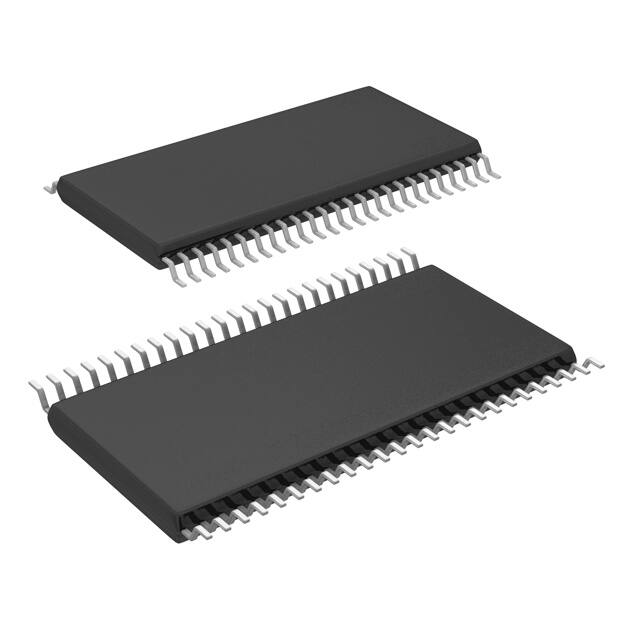
Packaged in Thin Shrink Small-Outline
Package (TSSOP) With 20-Mil Terminal
Pitch
Consumes Less Than 1 mW When Disabled
Wide Phase-Lock Input Frequency Range
of 31 MHz to 68 MHz
No External Components Required for PLL
Inputs Meet or Exceed the Standard
Requirements of ANSI EIA/TIA-644
Standard
Improved Replacement for the DS90C364
and SN75LVDS86
Improved Jitter Tolerance
See SN65LVDS86A-Q1 Data Sheet for
Information About the Automotive
Qualified Version
DGG PACKAGE
(TOP VIEW)
D17
D18
GND
D19
D20
NC
LVDSGND
A0M
A0P
A1M
A1P
LVDSVCC
LVDSGND
A2M
A2P
CLKINM
CLKINP
LVDSGND
PLLGND
PLLVCC
PLLGND
SHTDN
CLKOUT
D0
1
48
2
47
3
46
4
45
5
44
6
43
7
42
8
41
9
40
10
39
11
38
12
37
13
36
14
35
15
34
16
33
17
32
18
31
19
30
20
29
21
28
22
27
23
26
24
25
VCC
D16
D15
D14
GND
D13
VCC
D12
D11
D10
GND
D9
VCC
D8
D7
D6
GND
D5
D4
D3
VCC
D2
D1
GND
NC − Not connected
description
The SN65LVDS86A/SN75LVDS86A FlatLinkt receiver contains three serial-in 7-bit parallel-out shift registers
and four low-voltage differential signaling (LVDS) line receivers in a single integrated circuit. These functions
allow receipt of synchronous data from a compatible transmitter, such as the SN75LVDS81, ’83, ’84, or ’85, over
four balanced-pair conductors and expansion to 21 bits of single-ended low-voltage LVTTL synchronous data
at a lower transfer rate.
When receiving, the high-speed LVDS data is received and loaded into registers at seven times the LVDS input
clock (CLKIN) rate. The data is then unloaded to a 21-bit-wide LVTTL parallel bus at the CLKIN rate. The
’LVDS86A presents valid data on the falling edge of the output clock (CLKOUT).
The ’LVDS86A requires only four line-termination resistors for the differential inputs and little or no control. The
data bus appears the same at the input to the transmitter and output of the receiver with the data transmission
transparent to the user(s). The only user intervention is the possible use of the shutdown/clear (SHTDN)
active-low input to inhibit the clock and shut off the LVDS receivers for lower power consumption. A low level
on this signal clears all internal registers to a low level.
The SN75LVDS86A is characterized for operation over ambient free-air temperatures of 0_C to 70_C. The
SN65LVDS86A is characterized for operation over the full Automotive temperature range of − 40°C to 125°C.
Please be aware that an important notice concerning availability, standard warranty, and use in critical applications of
Texas Instruments semiconductor products and disclaimers thereto appears at the end of this data sheet.
FlatLink is a trademark of Texas Instruments Incorporated.
Copyright 2007, Texas Instruments Incorporated
���������� � � ����������� �� !"��#�� �� �� $"%
�!����� &��#'
���&"!�� !������ �� �$#!���!������ $#� �(# �#��� �� �#)�� �����"�#���
����&��& *������+' ���&"!���� $��!#����, &�#� ��� �#!#�����
+ ��!
"&#
�#����, �� �
$����#�#��'
POST OFFICE BOX 655303
• DALLAS, TEXAS 75265
1
�����������
����������
�
������ ��������
SLLS318D − NOVEMBER 1998 − REVISED NOVEMBER 2007
functional block diagram
Serial-In/ParallelOut Shift Register
A0P
A0M
Serial In
CLK
A, B, ...G
Serial-In/ParallelOut Shift Register
A1P
A1M
D0
D1
D2
D3
D4
D5
D6
Serial In
A, B, ...G
CLK
Serial-In/ParallelOut Shift Register
A2P
A2M
Serial In
D7
D8
D9
D10
D11
D12
D13
A, B, ...G
CLK
Control Logic
SHTDN
D14
D15
D16
D17
D18
D19
D20
Clock Generator
CLK
Clock In
CLKINP
CLKINM
Clock Out
Input Bus
2
POST OFFICE BOX 655303
• DALLAS, TEXAS 75265
CLKOUT
�����������
����������
�
������ ��������
CLKIN
ÇÇ
ÇÇ
ÉÉÉ
ÉÉÉ
Previous Cycle
D0−1
D6
A1
D7−1
A2
D14−1
ÇÇ
ÇÇ
ÉÉ
ÉÉ
Current Cycle
A0
CLKOUT
ÇÇ
ÇÇ
SLLS318D − NOVEMBER 1998 − REVISED NOVEMBER 2007
Next Cycle
D5
D4
D3
D2
D1
D0
D6+1
D13
D12
D11
D10
D9
D8
D7
D13+1
D20
D19
D18
D17
D16
D15
D14
D20+1
ÉÉÉ
ÉÉÉ
ÇÇ
ÇÇ
ÉÉ
ÉÉ
Dn − 1
D0
ÇÇÇ
ÇÇÇ
ÇÇ
ÇÇ
Dn
Dn + 1
Figure 1. SN65LVDS86A/SN75LVDS86A Load and Shift Timing Sequences
equivalent input and output schematic diagrams
VCC
300 kΩ
VCC
300 kΩ
5Ω
100 Ω
D Output
100 Ω
AnM
AnP
7V
7V
7V
VCC
OUTPUT
INPUT
SHTDN
50 Ω
7V
INPUT
POST OFFICE BOX 655303
• DALLAS, TEXAS 75265
3
�����������
����������
�
������ ��������
SLLS318D − NOVEMBER 1998 − REVISED NOVEMBER 2007
absolute maximum ratings over operating free-air temperature range (unless otherwise noted)†
Supply voltage range, VCC (see Note 1) . . . . . . . . . . . . . . . . . . . . . . . . . . . . . . . . . . . . . . . . . . . . . . . . . . . . −0.5 V to 4 V
Voltage range at any terminal . . . . . . . . . . . . . . . . . . . . . . . . . . . . . . . . . . . . . . . . . . . . . . . . . −0.5 V to VCC + 0.5 V
Electrostatic discharge (see Note 2): All pins (Class 3A) . . . . . . . . . . . . . . . . . . . . . . . . . . . . . . . . . . . . . . . . 4 KV
All pins (Class 2B) . . . . . . . . . . . . . . . . . . . . . . . . . . . . . . . . . . . . . . . 200 V
Continuous total power dissipation . . . . . . . . . . . . . . . . . . . . . . . . . . . . . . . . . . . . . . See Dissipation Rating Table
Operating virtual junction temperature range, TJ . . . . . . . . . . . . . . . . . . . . . . . . . . . . . . . . . . . . . . −40_C to 150_C
Storage temperature range, Tstg . . . . . . . . . . . . . . . . . . . . . . . . . . . . . . . . . . . . . . . . . . . . . . . . . . . . −65_C to 150_C
Lead temperature 1,6 mm (1/16 in) from case for 10 s . . . . . . . . . . . . . . . . . . . . . . . . . . . . . . . . . . . . . . . . . 260_C
† Stresses beyond those listed under “absolute maximum ratings” may cause permanent damage to the device. These are stress ratings only, and
functional operation of the device at these or any other conditions beyond those indicated under “recommended operating conditions” is not
implied. Exposure to absolute-maximum-rated conditions for extended periods may affect device reliability.
NOTES: 1. All voltage values are with respect to the GND terminals unless otherwise noted.
2. This rating is measured using MIL-STD-883C Method, 3015.7.
DISSIPATION RATING TABLE
PACKAGE
TA ≤ 25°C
POWER RATING
DERATING FACTOR‡
ABOVE TA = 25°C
TA = 70°C
POWER RATING
TA = 125°C
POWER RATING
DGG
1637 mW
13.1 mW/°C
1048 mW
327 mW
‡ This is the inverse of the junction-to-ambient thermal resistance when board mounted and with no air flow.
recommended operating conditions (see Figure 2)
MIN
Supply voltage, VCC
3
High-level input voltage, VIH (SHTDN)
2
NOM
MAX
UNIT
3.6
V
3.3
V
Low-level input voltage, VIL (SHTDN)
Magnitude differential input voltage, |VID|
0.1
|V
ID
2
Common-mode input voltage, VIC
Operating free-air temperature, TA
|
0.8
V
0.6
V
2.4 *
|V
ID
2
SN75LVDS86A
0
70
SN65LVDS86A
−40
125
|
V
°C
timing requirements
Cycle time, input clock, tc§
§ Parameter tc is defined as the mean duration of a minimum of 32 000 clock cycles.
4
POST OFFICE BOX 655303
• DALLAS, TEXAS 75265
MIN
NOM
MAX
UNIT
14.7
tc
32.4
ns
�����������
����������
�
������ ��������
SLLS318D − NOVEMBER 1998 − REVISED NOVEMBER 2007
electrical characteristics over recommended operating conditions (unless otherwise noted)
PARAMETER
TEST CONDITIONS
VIT+
Positive-going differential input threshold voltage
VIT−
Negative-going differential input threshold voltage‡
VOH
VOL
High-level output voltage
ICC
IIH
Disabled,
All inputs to GND
Enabled,
AnM = 1.4 V,
AnP = 1 V,
tc = 15.38 ns
UNIT
100
mV
mV
V
33
0.4
V
280
µA
40
43
Enabled,
CL = 8 pF,
Worst-case pattern (see Figure 4)
tc = 15.38 ns
VIH = VCC
High-level input current (SHTDN)
MAX
2.4
Enabled,
CL = 8 pF,
Grayscale pattern (see Figure 3),
tc = 15.38 ns
Quiescent current (average)
TYP†
−100
IOH = − 4 mA
IOL = 4 mA
Low-level output voltage
MIN
mA
68
±20
SN75LVDS86A
±20
SN65LVDS86A
±25
µA
µA
A
IIL
Low-level input current (SHTDN)
VIL = 0
II
IOZ
Input current A inputs
0 ≤ VI ≤ 2.4 V
±20
µA
High-impedance output current
VO = 0 or VCC
±10
µA
† All typical values are at VCC = 3.3 V, TA = 25°C.
‡ The algebraic convention, in which the less-positive (more-negative) limit is designated minimum, is used in this data sheet for the negative-going
input voltage threshold only.
switching characteristics over recommended operating conditions (unless otherwise noted)
PARAMETER
tsu
th
TEST CONDITIONS
Setup time, D0–D20 to CLKOUT↓
CL = 8 pF, See Figure 5
Data hold time, CLKOUT↓ to D0–D20
MIN
TYP†
MAX
UNIT
5
ns
5
ns
t(RSKM) Receiver input skew margin§ (see Figure 7)
tc = 15.38 ns (± 0.2%),
|Input clock jitter| < 50 ps¶,
td
Delay time, CLKIN↑ to CLKOUT↓ (see Figure 7)
VCC = 3.3 V,
tc = 15.38 ns (± 0.2%), TA = 25°C
ten
Enable time, SHTDN to phase lock
See Figure 7
1
ms
tdis
Disable time, SHTDN to off state
See Figure 8
400
ns
tt
tt
Transition time, output (10% to 90% tr or tf) (data only)
CL = 8 pF
3
ns
Transition time, output (10% to 90% tr or tf) (clock only)
CL = 8 pF
1.5
ns
550
700
3
5
ps
7
ns
tw
Pulse duration, output clock
0.50 tc
ns
† All typical values are at VCC = 3.3 V, TA = 25°C.
§ The parameter t(RSKM) is the timing margin available to allocate to the transmitter and interconnection skews and clock jitter. The value of this
parameter at clock periods other than 15.38 ns can be calculated from tRSKM = tc/14 – 550 ps.
¶ |Input clock jitter| is the magnitude of the change in input clock period.
POST OFFICE BOX 655303
• DALLAS, TEXAS 75265
5
�����������
����������
�
������ ��������
SLLS318D − NOVEMBER 1998 − REVISED NOVEMBER 2007
PARAMETER MEASUREMENT INFORMATION
AP
VIAP
(VIAP + VIAM)/2
VID
AM
VIC
VIAM
Figure 2. Voltage Definitions
CLKIN/CLKOUT
D0, D6, D12
D1, D7, D13
D2, D8, D14
D3, D9, D15
D18, D19, D20
ALL OTHERS
NOTE A: The 16-grayscale test-pattern test device power consumption for a typical display pattern.
Figure 3. 16-Grayscale Test-Pattern Waveforms
tc
CLKIN/CLKOUT
Even Dn
Odd Dn
NOTE A: The worst-case test pattern produces nearly the maximum switching frequency for all of the LVTTL outputs.
Figure 4. Worst-Case Test-Pattern Waveforms
6
POST OFFICE BOX 655303
• DALLAS, TEXAS 75265
�����������
����������
�
������ ��������
SLLS318D − NOVEMBER 1998 − REVISED NOVEMBER 2007
PARAMETER MEASUREMENT INFORMATION
tsu
70% VOH
D0 −D20
30% VOH
th
70% VOH
CLKOUT
30% VOH
Figure 5. Setup and Hold Time Waveforms
POST OFFICE BOX 655303
• DALLAS, TEXAS 75265
7
�����������
����������
�
������ ��������
SLLS318D − NOVEMBER 1998 − REVISED NOVEMBER 2007
PARAMETER MEASUREMENT INFORMATION
Tektronix
HFS9003/HFS9DG1
Stimulus System
(repeating patterns of
1110111 and 0001000)
An
D0 − D20
Device
Under
Test
(DUT)
CLKIN
Tektronix
Microwave Logic
Multi-BERT-100RX
Word Error Detector
CLKOUT
tc
Internal Strobing Position
4 t ±t
7 c (RSKM)
(see Note A)
tsu1
th1
3 t t
±
7 c (RSKM)
(see Note A)
ÉÉÉÇÇ
ÉÉÉÇÇ
ÇÇÇÉÉ
ÇÇÇÉÉ
An
and An
ÉÉÉÇÇ
ÉÉÉÇÇ
ÇÇÇÉÉ
ÇÇÇÉÉ
CLKIN
td
tW
CLKOUT
tr < 1 ns
90%
CLKIN
or An
≈ 300 mV
0V
10%
≈ −300 mV
tW
td
VOH
1.4 V
VOL
CLKOUT
NOTE A: CLKIN is advanced or delayed with respect to data until errors are observed at the receiver outputs. The advance or delay is then
reduced until there are no data errors observed. The magnitude of the advance or delay is t(RSKM).
Figure 6. Receiver Input Skew Margin, Setup/Hold Time, and Delay Time Definitions
8
POST OFFICE BOX 655303
• DALLAS, TEXAS 75265
�����������
����������
�
������ ��������
SLLS318D − NOVEMBER 1998 − REVISED NOVEMBER 2007
PARAMETER MEASUREMENT INFORMATION
CLKIN
An
ten
SHTDN
ÉÉÉÉÉÉÉÉÉÉÉÉÉÉÉÉÉÉÉÉÉÉÉÉÉÉ
ÉÉÉÉÉÉÉÉÉÉÉÉÉÉÉÉÉÉÉÉÉÉÉÉÉÉ
Dn
Invalid
Valid
Figure 7. Enable Time Waveforms
CLKIN
tdis
SHTDN
CLKOUT
Figure 8. Disable Time Waveforms
POST OFFICE BOX 655303
• DALLAS, TEXAS 75265
9
�����������
����������
�
������ ��������
SLLS318D − NOVEMBER 1998 − REVISED NOVEMBER 2007
TYPICAL CHARACTERISTICS
SUPPLY CURRENT
vs
CLOCK FREQUENCY
60
I CC − Supply Current − mA
55
VCC = 3.6 V
50
45
40
VCC = 3.3 V
35
Grayscale Data Pattern
CL = 8 pF
TA = 25°C
30
VCC = 3 V
25
30
40
50
60
70
80
90
fclk − Clock Frequency − MHz
Figure 9. RMS Grayscale ICC vs Clock Frequency
10
POST OFFICE BOX 655303
• DALLAS, TEXAS 75265
�����������
����������
�
������ ��������
SLLS318D − NOVEMBER 1998 − REVISED NOVEMBER 2007
APPLICATION INFORMATION
Host
Cable
Flat Panel Display
SN75LVDS84/5
Y0M
41
8
100 Ω
Y0P
Y1M
40
9
39
10
100 Ω
Y1P
Y2M
38
11
35
14
100 Ω
Y2P
CLKOUTM
34
15
33
16
100 Ω
CLKOUTP
32
17
SN75LVDS86A/
SN65LVDS86A
D0
A0M
D1
D2
D3
A0P
D4
D5
D6
A1M
D7
D8
D9
A1P
D10
D11
D12
A2M
D13
D14
D15
A2P
D16
D17
D18
CLKINM
D19
D20
CLKOUT
CLKINP
Graphics Controller
24
26
27
29
30
31
33
34
35
37
39
40
41
43
45
46
47
1
2
4
5
23
12-BIT
RED0
RED1
RED2
RED3
NA
NA
GREEN0
GREEN1
GREEN2
GREEN3
NA
NA
BLUE0
BLUE1
BLUE2
BLUE3
NA
NA
H_SYNC
V_SYNC
ENABLE
CLOCK
18-BIT
RED0
RED1
RED2
RED3
RED4
RED5
GREEN0
GREEN1
GREEN2
GREEN3
GREEN4
GREEN5
BLUE0
BLUE1
BLUE2
BLUE3
BLUE4
BLUE5
H_SYNC
V_SYNC
ENABLE
CLOCK
NOTES: A. The four 100-Ω terminating resistors are recommended to be 0603 types.
B. NA - not applicable, these unused inputs should be left open.
Figure 10. 18-Bit Color Host to Flat Panel Display Application
POST OFFICE BOX 655303
• DALLAS, TEXAS 75265
11
�����������
����������
�
������ ��������
SLLS318D − NOVEMBER 1998 − REVISED NOVEMBER 2007
APPLICATION INFORMATION
Host
Cable
Flat Panel Display
SN75LVDS81/83
Y0M
48
8
SN75LVDS86A/
SN65LVDS86A
A0M
100 Ω
Y0P
Y1M
47
9
46
10
A0P
A1M
100 Ω
Y1P
Y2M
45
11
42
14
A1P
A2M
100 Ω
Y2P
41
15
40
16
CLKOUTM
A2P
CLKINM
100 Ω
CLKOUTP
Y3M
Y3P
39
17
CLKINP
D0
D1
D2
D3
D4
D5
D6
D7
D8
D9
D10
D11
D12
D13
D14
D15
D16
D17
D18
D19
D20
CLKOUT
Graphics Controller
24
26
27
29
30
31
33
34
35
37
39
40
41
43
45
46
47
1
2
4
5
23
12-BIT
RED0
RED1
RED2
RED3
NA
NA
GREEN0
GREEN1
GREEN2
GREEN3
NA
NA
BLUE0
BLUE1
BLUE2
BLUE3
NA
NA
H_SYNC
V_SYNC
ENABLE
CLOCK
38
37
NOTES: A. The four 100-Ω terminating resistors are recommended to be 0603 types.
B. NA - not applicable, these unused inputs should be left open.
Figure 11. 24-Bit Color Host to 18-Bit Color LCD Panel Display Application
See the FlatLinkt Designer’s Guide (SLLA012) for more application information.
12
POST OFFICE BOX 655303
• DALLAS, TEXAS 75265
18-BIT
RED0
RED1
RED2
RED3
RED4
RED5
GREEN0
GREEN1
GREEN2
GREEN3
GREEN4
GREEN5
BLUE0
BLUE1
BLUE2
BLUE3
BLUE4
BLUE5
H_SYNC
V_SYNC
ENABLE
CLOCK
�PACKAGE OPTION ADDENDUM
www.ti.com
14-Oct-2022
PACKAGING INFORMATION
Orderable Device
Status
(1)
Package Type Package Pins Package
Drawing
Qty
Eco Plan
(2)
Lead finish/
Ball material
MSL Peak Temp
Op Temp (°C)
(3)
Device Marking
Samples
(4/5)
(6)
SN65LVDS86AQDGG
ACTIVE
TSSOP
DGG
48
40
RoHS & Green
NIPDAU
Level-2-260C-1 YEAR
-40 to 125
65LVDS86AQ
Samples
SN65LVDS86AQDGGR
ACTIVE
TSSOP
DGG
48
2000
RoHS & Green
NIPDAU
Level-2-260C-1 YEAR
-40 to 125
65LVDS86AQ
Samples
SN75LVDS86ADGG
ACTIVE
TSSOP
DGG
48
40
RoHS & Green
NIPDAU
Level-2-260C-1 YEAR
0 to 70
SN75LVDS86A
Samples
SN75LVDS86ADGGR
ACTIVE
TSSOP
DGG
48
2000
RoHS & Green
NIPDAU
Level-2-260C-1 YEAR
SN75LVDS86A
Samples
(1)
The marketing status values are defined as follows:
ACTIVE: Product device recommended for new designs.
LIFEBUY: TI has announced that the device will be discontinued, and a lifetime-buy period is in effect.
NRND: Not recommended for new designs. Device is in production to support existing customers, but TI does not recommend using this part in a new design.
PREVIEW: Device has been announced but is not in production. Samples may or may not be available.
OBSOLETE: TI has discontinued the production of the device.
(2)
RoHS: TI defines "RoHS" to mean semiconductor products that are compliant with the current EU RoHS requirements for all 10 RoHS substances, including the requirement that RoHS substance
do not exceed 0.1% by weight in homogeneous materials. Where designed to be soldered at high temperatures, "RoHS" products are suitable for use in specified lead-free processes. TI may
reference these types of products as "Pb-Free".
RoHS Exempt: TI defines "RoHS Exempt" to mean products that contain lead but are compliant with EU RoHS pursuant to a specific EU RoHS exemption.
Green: TI defines "Green" to mean the content of Chlorine (Cl) and Bromine (Br) based flame retardants meet JS709B low halogen requirements of


 工商网监
湘ICP备2023018690号
工商网监
湘ICP备2023018690号
