SP16160CH1RBKIT/NOPB 数据手册
SP16160CH1RB
High-IF Receiver Reference Design Board
LMH6517 + ADC16DV160 + LMK04031B
User’s Guide
1.0 Reference Board Overview
2
2.0 Evaluation Kit Contents
4
3.0 System Description
4
4.0 Data Capture
5
5.0 Quick Start
5
6.0 Functional Description
7
7.0 System Performance
11
8.0 Device Configuration
13
9.0 Optional Hardware Configurations
17
10.0 Schematic
19
11.0 Layout
23
12.0 Bill of Materials
29
www.national.com
Rev 2.2
September 2009
�SP16160CH1RB Reference Design Board User’s Guide
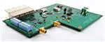
1.0 Reference Board Overview
Manual DVGA
Gain Control (Optional)
FutureBus
Connector
SMA_AMP_I:
In-Phase
Analog Input
LMH
6517
ADC
16DV160
SMA_AMP_Q:
Quadrature
Analog Input
SAW &
Clock
Buffer
VCXO
(76.8 MHz)
LMK
04031B
Low Noise
Regulators
Reference
Crystal
Oscillator
(61.44 MHz)
H3: uWire
Header
+5.0V
Power
Connector
JP1
Figure 1: SP16160CH1RB board (front side)
-2-
www.national.com
�SP16160CH1RB Reference Design Board User’s Guide
Switching
Regulators
Varactor
Controlled
Crystal XO
(Optional)
Figure 2: SP16160CH1RB board (back side)
-3-
www.national.com
�SP16160CH1RB Reference Design Board User’s Guide
SP16160CH1RB Reference Board
1:4
16-bit, 8-lane
DDR Interleaved
LVDS Digital Data
ADC – I
6-bit Gain
Control
VRM
LMH6517
FutureBus
Connector
DVGA – I
ADC16DV160
DVGA – Q
16-bit, 8-lane
DDR Interleaved
LVDS Digital Data
ADC – Q
VA 3.0V
+5V
LM2734
61.44 MHz
Crystal Oscillator
Reference
LP3878-ADJ
153.6 MHz
SAW Filter
CLK+
CLK-
VA 1.8V
LM2734
LMK04031B
LP3878-ADJ
Low Noise
CMOS
Buffer
153.6 MHz
CMOS
Sampling
Clock
VD 1.8V
LP5900
76.8 MHz
Voltage Controlled
Crystal Oscillator
VPLL 3.3V
LP3878-ADJ
VXO 3.3V
PLL2 External
Loop Filter
Components
PLL1 External
Loop Filter
Components
LP5900
Figure 3: SP16160CH1RB block diagram
2.0 Evaluation Kit Contents
3.0 System Description
The SP16160CH1RB evaluation kit includes the
following items:
The SP16160CH1RB is a high IF receiver reference
design board that utilizes the following components
from National Semiconductor:
•
SP16160CH1RB reference design board
•
PIC microcontroller board (ADC14PIC REV. A)
•
The SP16160CH1RB reference board is fully
assembled for immediate evaluation. A PIC
microcontroller board is included with the evaluation kit
to properly configure the on-board clock solution.
ADC16DV160 A dual channel, 16-bit, 160 MSPS
(Megasamples-per-second)
analog-to-digital
converter (ADC) with parallel LVDS outputs.
•
LMH6517 A high performance, dual channel
digitally controlled variable gain amplifier (DVGA)
with a 31.5 dB gain range in 0.5 dB steps.
The following items are required to evaluate the
SP16160CH1RB but NOT included in the evaluation
kit. See section 5.0 Quickstart for more information.
•
LMK04031B A clock conditioning solution
composed of a low-noise jitter cleaner, clock
multiplier, and clock distribution stage.
•
Several energy-efficient power management ICs
including the LM2734 switching regulator and the
LP3878-ADJ and LP5900 low drop-out (LDO)
regulators.
•
Signal generator and connecting cables
•
+5V, 1A power supply and cable
•
Data capture hardware and analysis software
-4-
www.national.com
�SP16160CH1RB Reference Design Board User’s Guide
Figure 4: Connection diagram for the SP16160CH1RB board and WaveVision 5.1 data capture hardware
As shown in block diagram of Figure 3, this subsystem
reference
design
provides
single-to-differential
conversion, digitally controlled gain, bandpass filtering
of dual channel input signals and high dynamic range
digitization. The low-noise optimized clock path
provides a 153.6 MHz low-jitter, single-ended CMOS
sampling clock for the ADC.
The measured system performance demonstrates an
Nyquist band SNR of 72 dBFS for a -3 dBFS, 192 MHz
input signal and SFDR greater than 85 dBFS for single
tone input frequencies between 182 and 202 MHz and
a sampling frequency of 153.6 MSPS.
This reference design enables immediate evaluation of
a high dynamic range, high-IF sampling application
such as a wireless communications sampling receiver
subsystem.
Interface Board and associated WaveVision 5
software. Please note that the SP16160CH1RB board
is not compatible with previous versions of the
WaveVision hardware (WaveVision 4.x Digital Interface
Boards).
The WaveVision hardware and software package
allows fast and easy data acquisition and analysis. The
WaveVision hardware connects to a host PC via a USB
cable and is fully configured and controlled by the latest
WaveVision software.
The latest version of the
WaveVision 5 software and information about the
WaveVision 5.1 Signal Path Digital Interface hardware
(part number: WAVEVSN BRD 5.1) are available
through the National Semiconductor website at
http://www.national.com/analog/adc.
5.0 Quick Start
4.0 Data Capture
5.1 WaveVision Software and Hardware Installation
The digital data from the SP16160CH1RB reference
design board can be captured with a suitable
instrument, such as a logic analyzer, or with National
Semiconductor’s WaveVision signal path data
acquisition hardware and software platform.
The
SP16160CH1RB board is connected to the data
acquisition hardware through the FutureBus connector
(schematic reference designator H4).
•
Begin by installing the latest version of WaveVision
5 and be sure to enable the update manager to
keep up to date with the most current version. Do
not start the WaveVision software application at
this point.
The WaveVision software must be installed
before connecting the WaveVision hardware.
The SP16160CH1RB is compatible with National
Semiconductor’s WaveVision 5.1 Signal Path Digital
-5-
www.national.com
�SP16160CH1RB Reference Design Board User’s Guide
•
Connect the WaveVision 5.1 Digital Interface
Board to your PC through the supplied USB cable
and apply power to the WaveVision 5.1 board
through the +12V AC-DC power adapter included
in the WaveVision 5.1 hardware kit.
The
connection diagram is shown in Figure 4.
If this is the first time connecting a WaveVision 5.1
board to your PC, follow the on-screen instructions for
installing the drivers for the hardware.
•
Press the “RESET” button on the PIC
microcontroller to load the register settings into the
LMK04031B.
The three LED’s on the PIC
microcontroller board will flash four times to
indicate that the register bits have been sent to the
LMK04031B. If the lights to not flash, ensure that
JP1 is connected to supply power to the PIC board.
•
Connect the signal source to the “SMA_AMP_I”
SMA connector indicated in Figure 1.
The
recommended signal generators are the HP8644B
(HP/Agilent) or the SMA100A (Rohde & Schwarz).
A bandpass filter between the signal generator
output and the SP16160CH1RB SMA connector is
required to measure the true performance of the
board. A Trilithic bandpass filter is recommended.
See Figure 4.
•
Set the signal source frequency to 190 MHz and
the starting input amplitude to -15 dBm.
•
Start the WaveVision software. The WaveVision
software will automatically load the appropriate
firmware to initialize data capture from the
SP16160CH1RB. Allow the firmware file to finish
downloading before continuing. When finished, the
board should be ready to capture digital data.
•
Capture the data and display the FFT of the
captured data with the WaveVision software.
For more information on installing the WaveVision data
acquisition hardware or software, please refer to the
Quick Start Guide in the WaveVision User’s Guide
which can be found on the National Semiconductor
website
at
http://www.national.com/
appinfo/adc/evalboards_datacapture.html.
Please note that the SP16160CH1RB is only
compatible with National Semiconductor’s WaveVision
5.1 Digital Interface board.
5.2 Reference Board Jumper Positions
•
Verify that the JP1 jumper is installed to provide
power to the PIC microcontroller board. The PIC is
used for programming the LMK04031B registers.
Remove JP1 if using CodeLoader to program the
LMK04031B (see Section 8.2 of this guide).
5.3 Connecting Power and Signal Sources
•
•
•
•
Switch 1 = ON
Switch 2 = ON
Connect the SP16160CH1RB reference board to
the WaveVision 5.1 board through the FutureBus
connector as shown in Figure 4.
The
SP16160CH1RB reference board should not be
powered up, as the WaveVision hardware does not
support hot-swapping of boards.
Place JP1 on
main board to
provide power
to PIC board
Power up the WaveVision 5.1 board and connect it
to the PC with a USB cable.
Plug the PIC microcontroller board onto the dualrow header labeled “H3” as shown in Figure 5.
Align the arrows on the two boards to ensure
proper orientation. JP1 should have a jumper
installed on the main board to provide power to the
PIC microcontroller board. Lastly, flip the switches
on the PIC microcontroller board to the following
positions: Switch 1 = ON, Switch 2 = ON.
Align Pin
1 Arrows
Figure 5: PIC microcontroller Board Connection
and Configuration
Connect a 5.0V power supply capable of sourcing
up to 1A to the green, 2-terminal power connector
located along the side edge of the SP16160CH1RB
board. This is shown in Figure 4. Ensure that the
polarity of the wires going to the green power
connector match the “+5V” and “GND” labels on
the reference board. After the polarity is verified,
turn on the 5V supply.
-6-
www.national.com
�SP16160CH1RB Reference Design Board User’s Guide
Figure 6: Single channel analog input signal path
6.0 Functional Description
6.1 Signal Path
The critical signal path of the SP16160CH1RB travels
from the signal source input through a transformer, the
DVGA, a bandpass filter, and then to the ADC. Circuit
details are shown in Figure 6.
loss. The source resistors and 3 pF shunt capacitor at
the DVGA output are necessary to maintain amplifier
stability and provide an adequate passband profile.
The ADC samples the input signal at 153.6 MSPS,
quantizes it to 16-bits, and outputs LVDS data. The full
scale input range of the ADC is 2.4 V differential peakto-peak (Vdiff-PP) and must be fully utilized to maximize
the SNR performance.
Table 1: Bandpass filter component values
A transformer is necessary to match the 50 ohm
impedance of the signal generator to the 200 ohm input
impedance of the LMH6517. The 1:4 impedance ratio
of the transformer provides ~6 dB of voltage gain at the
input of the DVGA. AC coupling capacitors isolate the
internal common-mode bias of the DVGA from the
grounded center tap of the transformer.
LD
[nH]
LU
[nH]
CDU
[pF]
CT1
[pF]
CT2
[pF]
LT
[nH]
192
20
110
200
4
16
4
33
0
0
Magnitude [dB]
-10
The T-matched bandpass anti-aliasing filter between
the LMH6517 DVGA and the ADC16DV160 provides
attenuation of amplifier distortion and noise. The
SP16160CH1RB filter has been designed for an
intermediate frequency (IF) of 192 MHz and a 20 MHz
bandwidth.
Filter component values for the circuit in Figure 6 are
given in Table 1 and the normalized filter profile is
shown in Figure 7. The load resistors of the filter are
chosen to provide a low impedance input commonmode reference for the ADC and 0 dB voltage insertion
BW
[MHz]
10
The DVGA is composed of a ladder attenuator followed
by a 22 dB, fixed-gain amplifier. The ladder has a 31.5
dB attenuation range in 0.5 dB steps and is controlled
by a 6-bit internal register.
Frequencies above the bandpass center have greater
th
than 4 order roll-off (> 24dB/octave) with this filter
st
topology whereas low frequencies have only a 1 order
roll-off. This architecture can provide > 40 dB harmonic
attenuation with minimal filter complexity and nearly 0
dB insertion loss to allow the DVGA to drive the ADC
input to full scale without compressing at the supply
rails. Ripple in the passband is easily kept below 1 dB.
The equivalent noise bandwidth (ENBW) of this filter is
approximately 44 MHz.
Center
Frequency
[MHz]
-2
-20
-4
-30
-6
160
180
200
220
[MHz]
-40
-50
-60
-70
0
200
400
600
Frequency [MHz]
Figure 7: Bandpass filter profile centered at 192 MHz
A low noise signal generator such as the HP8644B
(HP/Agilent) or SMA100A (Rohde & Schwarz) is
recommended to drive the signal input of the
SP16160CH1RB evaluation board. The output of the
signal generator must be filtered to suppress the
harmonic distortion and noise produced by the signal
generator and to allow accurate measurement of the
system’s distortion performance. A tunable bandpass
filter made by Trilithic (Indianapolis, IN) is
-7-
www.national.com
�CpOut2
OSCin
CpOut1
SP16160CH1RB Reference Design Board User’s Guide
Figure 9: Sampling clock path of the SP16160CH1RB
recommended. Using only a lowpass filter is not
recommended as the SNR performance is significantly
degraded by the broad-band signal generator noise in
the passband.
The ADC has an internal register option to reduce the
reference voltage for improved distortion at the cost of
reduced SNR. The register can be configured using the
WaveVision 5 data capture platform.
6.2 IF-Sampling Sub-System Frequency Plan
6.4 Clock Path
The SP16160CH1RB sub-samples the 192 MHz IF
with a 153.6 MSPS clock so that the 20 MHz signal
band aliases to the center of the first Nyquist zone at
38.4 MHz.
The clock signal used to sample the analog input is
generated using the LMK04031B. The LMK04031B is a
low-jitter precision clock conditioner that consists of
cascaded phase locked loops (PLLs), an internal
voltage controlled oscillator (VCO) and a distribution
stage. The first PLL locks an external voltage controlled
crystal oscillator (VCXO) to an incoming reference
clock and filters the phase noise of the reference. The
output of the first PLL becomes the reference input to
the second PLL stage which uses a VCO to multiply the
external VCXO frequency. The VCO output is passed
to the distribution stage which provides frequency
division, buffering and conversion to a number of clock
output formats including CMOS, LVPECL and LVDS.
A large benefit of this plan is the placement of of the
second order harmonic, H2, completely out of the band
of interest when it aliases. H3 cannot be excluded from
the signal band and must be reduced in the system as
much as possible. The frequency ranges of the H2 and
H3 aliases are shown in Figure 8.
IF Band
20 MHz
H2
H3
[MHz]
38.4
76.8
Figure 8: Frequency plan showing aliasing of
the 192 MHz IF band, H2 band, and H3 band
into the first Nyquist zone
6.3 ADC Reference
The SP16160CH1RB reference board is configured to
use the internal 1.2V reference on the ADC16DV160.
This is the recommended reference configuration for
the ADC16DV160.
For a lower cost implementation, the first PLL can also
be configured to use an internal, low-noise oscillator
circuit with an external crystal and varactor diode.
In the SP16160CH1RB system shown in Figure 9, the
clock is generated with the LMK04031B by locking a
76.8 MHz VCXO (Crystek CVHD-950-76.8) to the
61.44 MHz reference oscillator, cleaning the phase
noise, multiplying the VCXO to 1536 MHz and then
dividing the frequency down to output a 153.6 MHz,
single-ended CMOS clock. The external loop filter
components for PLL1 and PLL2 are optimized for low
jitter performance.
The single-ended CMOS clock signal from the
LMK04031B is passed through a narrow bandwidth
SAW filter and then buffered with a low-noise CMOS
buffer to create a very low jitter, single-ended clock
source at the CLK+ input of the ADC16DV160. Filtering
-8-
www.national.com
�SP16160CH1RB Reference Design Board User’s Guide
and buffering the clock reduces broadband white noise
present on the clock output from the LMK04031B.
Reducing the broadband noise is important because
the noise present at the wideband clock input of the
ADC convolves with the input signal during the
sampling process and aliases back into the first Nyquist
zone to degrade the SNR. A capacitive divider is then
used to reduce the clock amplitude to within tolerable
levels for the ADC.
6.5 Output Data
The dual channel, 16-bit digitized outputs from the
SP16160CH1RB reference board consist of 38 lines
that are arranged into 17 LVDS pairs. These 17 pairs
of lines carry the 16-bit output data (16 pairs) and the
DRDY output clock signal (1 pair) across the FutureBus
connector on the edge of the reference board to the
data capture hardware.
The data is clocked out of the ADC using the DRDY
signal with a dual date rate (DDR) such that the even
bits of both channels are available on the rising edge of
DRDY while the odd bits are available on the falling
edge.
Channel I data is available on the reference board at
pins A5/B5 (MSB +/-) through A12/B12 (LSB +/-) of the
FutureBus connector and Channel Q data is available
at pins A14/B14 through A21/B21. The DRDY signal is
at pins A13/B13.
Please see the SP16160CH1RB reference board
schematic in Section 10.0 of this guide and the
ADC16DV160 datasheet for further details.
6.6 Power requirements.
Power to the SP16160CH1RB evaluation board is
supplied through the green power connector labeled
“POWER” located along the side edge of the board.
The power supply must be capable of sourcing +5V up
to 1A. The SP16160CH1RB reference board draws
approximately 800 mA when digitizing a full scale input.
-9-
www.national.com
�SP16160CH1RB Reference Design Board User’s Guide
Ch.I Average -1dBFS
SP16160CH1RB Typical SFDR
Ch.I Average -3dBFS
Ch.I Average -6dBFS
100
Ch.Q Average -1dBFS
Ch.Q Average -3dBFS
Ch.Q Average -6dBFS
Magnitude [dBFS]
95
90
85
80
75
181
186
191
196
201
Frequency [MHz]
Figure 10: Typical SFDR performance vs. input signal frequency
Ch.I Average -1dBFS
SP16160CH1RB Typical SNR
Ch.I Average -3dBFS
Ch.I Average -6dBFS
74
Ch.Q Average -1dBFS
Ch.Q Average -3dBFS
73.5
Ch.Q Average -6dBFS
Magnitude [dBFS]
73
72.5
72
71.5
71
70.5
70
181
186
191
196
201
Frequency [MHz]
Figure 11: Typical Nyquist-band SNR performance vs. input signal frequency
- 10 -
www.national.com
�SP16160CH1RB Reference Design Board User’s Guide
7.0 System Performance
insertion loss of the filter but will result in worse
intermodulation distortion.
Figure 10 and Figure 11 show the typical SFDR and
SNR performance respectively over frequency. The
input signal is measured at -1, -3, and -6 dBFS and the
sample rate is 153.6 MSPS. Figure 12 (a) and (b) show
typical spectra for single and two-tone signals near 192
MHz.
Jitter plays a role in limiting the SNR for large signal
inputs. A 192 MHz, -1 dBFS input signal yields phase
noise that results in an SNR, due to jitter (SNRJitter), of
~75 dBFS. This SNRJitter performance suggests a total
clock jitter of less than 200 fs.
7.1 Sources of Distortion
Harmonic distortion is introduced by the DVGA but
does not appear at the ADC input due to the high
attenuation of the anti-aliasing filter. Third-order
intermodulation distortion falls into the filter bandpass
and cannot be filtered out due to its proximity to the
bandwidth of interest. Two-tone test measurements
show that the third order products remain below 84
dBFS for a two-tone composite signal that has a 1 MHz
tone separation and swings 90% of full scale (-1 dBFS,
peak-to-peak).
The second- and third-order harmonic distortion (H2
and H3) that limits the SFDR of the system dominantly
occurs at the interface to the ADC. Charge kickback
from CMOS switches in the input stage of the ADC is a
significant cause of the harmonic distortion and can be
kept low with an empirical choice of capacitance in the
filter’s LC tank. Input signals near -1 dBFS amplitude
result in an SFDR typically greater than 82 dBFS
across the passband while -6 dBFS inputs typically
have an SFDR of greater than 92 as shown in Figure
10.
7.2 Sources of Noise
Combining the noise sources from the ADC, DVGA,
and clock results in the total SNR (SNRT) of 71 dBFS
for a -1 dBFS input signal as shown in Figure 11. SNRT
also improves for lower DVGA gain settings due to a
reduction in DVGA noise.
7.3 Wireless Base-Station Specific Performance
Base-station applications are concerned with
maximizing the sensitivity in a certain channel
bandwidth which can be limited by noise and spurs that
appear in the channel.
Blocking signals that appear close in frequency to the
channel not only limit the ability of the DVGA to apply
gain to the signal, but also contribute more noise to the
channel due to the phase noise skirt and the higher
broadband phase noise level that accompanies large
signals. To prevent overloading the ADC, a receiver’s
automation gain control (AGC) loop will keep the
blocking signal at a reasonable level such as -4 dBFS.
Assuming a GSM-type channel bandwidth of 200 kHz
and a -4 dBFS blocking signal that is 800 kHz from the
channel center, the SP16160CH1RB achieves a SNR
of 94 dBFS in the channel. In the absence of a blocking
signal, the system achieves a channel SNR of greater
than 99 dBFS.
The SNR of the SP16160CH1RB is limited by the
thermal noise in the DVGA, thermal noise in the ADC,
and the jitter on the sampling clock.
Thermal noise in the ADC sets the hard SNR limit in
the system. An ideal 16-bit ADC is capable of a 98
dBFS SNR if quantization noise is the only contributor.
Additional noise in the ADC16DV160 limits the small
signal SNR to 78 dBFS and large signal SNR to 76.5
for a 192 MHz signal.
The signal bandwidth of the anti-aliasing filter is 20
MHz, considered here as the bandwidth with 0.5 dB
ripple, but the effective noise bandwidth is 44 MHz due
to the gradual roll-off of the filter profile. Noise from the
DVGA passes through the filter bandpass to contribute
to the total noise of the system. With the LMH6517
output noise density of 22 nV/sqrt(Hz) at 192 MHz and
a 1 dB insertion loss through a filter with a 44 MHz
ENBW, the small signal SNR due to the DVGA noise
(SNRDVGA) is 76.3 dBFS. The SNRDVGA can be
improved using a filter with a narrower effective noise
bandwidth. It can also be improved by increasing the
- 11 -
www.national.com
�SP16160CH1RB Reference Design Board User’s Guide
IM3
IM2
H3
H2
H2
(a)
(b)
Figure 12: Typical FFT plot for a (a) 192 MHz, -1 dBFS input signal and (b) 194 MHz two-tone
composite signal with 1 MHz spacing and -7 dBFS tones
- 12 -
www.national.com
�SP16160CH1RB Reference Design Board User’s Guide
8.0 Device Configuration
8.1 ADC16DV160 and LMH6517 Programming
The ADC16DV160 and LMH6517 are both
programmable via a shared serial programming
interface (SPI) bus that is accessible on the FutureBus
connector. Writing to a device is handled with individual
chip selects and is transparent to the user when using
the WaveVision 5 capture platform and software.
Registers are programmed via the Registers tab in the
WaveVision 5 software as shown in Figure 13 and
Figure 14. After the reference board is been identified
by the software, the Registers tab appears on the righthand side of the window. Opening the tab reveals
options for modifying the individual registers with highlevel nomenclature.
Figure 13: ADC16DV160 Registers tab in
the WaveVision 5 software (Default)
ADC Device Registers (Figure 13)
•
Operation Mode: Changes the operation of the
ADC from normal operation to sleep, powerdown, or fixed pattern modes.
•
Data Format: Selects the output data format as
Offset Binary or 2’s Complement.
•
Full Scale Reference Voltage: Varies the
reference range of the ADC from 2.4 Vpp to
1.0 Vpp.
•
Sample Phase: Selects the sampling edge of
the clock.
•
Clock Divider: Sets the internal clock to be
divided by 1 or 2.
•
Output Clock Phase: Varies the phase offset of
the output data clock.
LMH Device Registers (Figure 14)
•
Ch. A/B Enable: Enables or disables the DVGA
output stage.
•
DVGA A/B Attenuation (bits): Varies the
attenuation of the ladder attenuator from 0 dB
(value = 0) to 31.5 dB (value = 64).
The ADC16DV160 can only be programmed via SPI
but the LMH6517 can operate in multiple modes.
These modes include a Serial Mode in which the
device is programmed via SPI, Parallel Mode in which
the gain of the DVGA is controlled by manual switches,
and Pulse Mode. The SP16160CH1RB is factory
configured for Serial Mode but can be modified to
operate in Parallel Mode. Pulse Mode is not supported
on the SP16160CH1RB. Refer to the Optional
Configurations section for more information.
Max
Attenuation
Figure 14: LMH6517 Registers tab in the
WaveVision 5 software
8.2 LMK04031B Programming
The LMK04031B, which provides the sample clock for
the ADC, must be configured correctly for the desired
clock frequency. Programming can be accomplished by
two methods.
The first method is to attach a small PIC-based module
that is included in this evaluation kit. This module is
plugged onto the 10-pin uWire header labeled “H3” as
described in section 5.3 of this user’s guide. If this
module is used, the JP1 jumper must be installed to
provide power from the main board to the PIC module.
The PIC module will program the LMK04031B to output
a 153.6 MHz single ended CMOS signal.
The second method for programming the LMK04031B
uses the 10-pin uWire header to connect the
LMK04031B’s serial programming interface (DATA,
CLK, LE) to a PC. To use this programming interface,
a special parallel port (LPT) cable supplied by National
Semiconductor allows the device to be directly
- 13 -
www.national.com
�SP16160CH1RB Reference Design Board User’s Guide
programmed with a PC using National Semiconductor’s
CodeLoader software.
The serial programming
interface can also be programmed over the USB port of
the PC. To program the LMK04031B through the USB
port, a separate interface board is available from
National Semiconductor.
See
http://www.national.com/appinfo/interface/clk_condition
ers.html to download CodeLoader, obtain a user’s
guide and to order any necessary hardware such as
programming cables or USB interface boards.
Remove JP1 if using CodeLoader to program the
LMK04031B.
The procedure for programming the LMK04031B
through National’s CodeLoader software and special
parallel port cable is described here if the user intends
to program the SP16160CH1RB reference board for
sampling rates other than 153.6 MSPS. Please note
that the achievable sample rates are limited by the
61.44 MHz reference crystal oscillator and the 76.8
MHz VCXO if they are used. Hardware changes are
also necessary to modify the clock path from the
standard 153.6 MHz path. Some output frequencies
may also require loop filter changes for optimal jitter
performance. In the default hardware configuration,
153.6 MHz is the only possible clock frequency due to
the narrowband SAW filter in the clock path.
Figure 17 through Figure 25 illustrate each CodeLoader
configuration screen and its contents used to properly
program the LMK04031B Clock Conditioner through
either a parallel port or USB PC interface and
appropriate cable. These configuration screens are for
programming the LMK04031B to output 153.6 MHz at
CLKout2, which is the same output produced by using
the PIC-module included in this evaluation kit.
Before programming the device, it is important that the
LMK04031B go through a proper reset cycle. Check
and then uncheck the RESET checkbox in the Bits/Pins
tab in Figure 18 to accomplish the reset. Then
configure the CodeLoader software according to the
following figures and select Load Device from the
Keyboard Controls file menu to program the device.
Figure 15: LMK04031B CodeLoader software communication port setup for programming
The user may be required to select a different LPT port that is compatible with the capabilities of the
PC being used to program the device. Using the USB port requires a separate interface board,
available from National Semiconductor.
- 14 -
www.national.com
�SP16160CH1RB Reference Design Board User’s Guide
Figure 16: LMK04031 CodeLoader configuration, Bits/Pins tab.
Figure 17: LMK04031B CodeLoader configuration, PLL1 tab.
- 15 -
www.national.com
�SP16160CH1RB Reference Design Board User’s Guide
Figure 18: LMK04031B CodeLoader configuration, PLL2 tab.
Using PLL parameter values different from the values shown in Figure 17 and Figure 18 may result
in degraded performance of the reference board.
Figure 19: LMK04031B CodeLoader configuration, Clock Outputs tab.
The LMK04031B clock outputs are not easily accessible on the SP16160CH1RB reference board.
See http://www.national.com/appinfo/interface/clk_conditioners.html for information on acquiring the
LMK04031B Evaluation board that provides full access to all clock outputs on the LMK04031B.
- 16 -
www.national.com
�SP16160CH1RB Reference Design Board User’s Guide
9.0 Optional Hardware Configurations
Part
Some optional hardware configurations are available
on the SP16160CH1RB to evaluate the sub-system
with different specified parameters and controls.
9.1 DVGA Gain DIP Switches
The SP16160CH1RB board is factory configured for
programmable control of the DVGA gain via the SPI
bus that is accessible on the FutureBus connector
H4. 8-position DIP switches can be installed in the
case that manual control of the gain is desired. The
following changes must be made to the reference
board to control the DVGA gain with switches. Table
2 gives the functions of the individual switches.
Sw #
Description
1
Latch (active high)
2
DVGA Enable (active high)
SWQ
3
Gain[0] (LSB)
(Controls
Q-Channel
DVGA)
4
Gain[1]
5
Gain[2]
6
Gain[3]
7
Gain[4]
8
Gain[5] (MSB, active high)
1
Gain[5] (MSB, active high)
2
Gain[4]
•
Remove R71-R78 and R91-R98.
SWI
3
Gain[3]
•
Populate R61-R68 and R81-R88 with 10k ohm,
0402 resistors.
4
Gain[2]
5
Gain[1]
•
Populate R71-R78 and R91-R98 with 20k ohm,
0402 resistors.
(Controls
I-Channel
DVGA)
6
Gain[0] (LSB)
•
Populate SWI and SWQ with 8-position, 10 mil
spaced DIP switches. Note the orientation of the
switch ON position in Figure 20.
7
DVGA Enable (active high)
8
Latch (active high)
•
•
Table 2: Function of optional DVGA DIP switches
Remove R32. Populate R31 and R32 with 11k
and 24k ohm, 0402 resistors respectively. These
footprints are located on the back of the board
under the DVGA.
9.2 Sampling Clock Options
Utilizing the SAW filter and CMOS buffer with a
single-ended CMOS clock optimizes the clock path
for minimal jitter. There are additional available
clocking schemes as listed below. Each non-default
option requires hardware and software modification of
the reference board.
Remove resistors R4-R7 located on the back side
by the FutureBus Connector.
1. External signal generator clock source
2. Single Ended CMOS with SAW and Buffer
(Default configuration)
3. Differential LVPECL
4. Differential CMOS
SWQ
The clock options above are listed in order from
potentially least jitter (#1) to most jitter (#4).
Perform the following changes to modify the board for
a 153.6 MHz differential LVPECL clock:
•
Remove R171, C174, C176 and C177
•
Populate R154, R155, R159, and R160 with 0
ohm, 0402 resistors
•
Populate R157 and R158 with 121 ohm, 0402
resistors
•
Populate C172 and C173 with 0.1uF, 0402
capacitors
SWI
Figure 20: Orientation of the DIP switches that
control the DVGA gain
- 17 -
www.national.com
�SP16160CH1RB Reference Design Board User’s Guide
•
Please contact National Semiconductor for more
information on configuring the reference board if this
option is desired.
Program the LMK04031B with the PIC Loader
board set with Switch 1 = ON, Switch 2 = OFF
Perform the following changes to modify the board for
a differential CMOS clock:
•
Remove R171, C174, C176 and C177
•
Populate R152, R153, R159 and R160 with 0
ohm, 0402 resistors
•
Populate C172 and C173 with 0.1uF, 0402
capacitors
•
This
mode
requires
programming
LMK04031B via the CodeLoader software
9.4 Bypassed Switching Regulators
LM2734 Switching regulators are utilized in this
reference board design to minimize LDO regulator
losses for the high current ADC supplies.
Noise on the supplies, especially the sensitive 1.8 V
analog supply to the ADC, can cause a performance
degradation in the form of small spurs offset ~500
kHz from a large input tone as shown in Figure 21.
These spurs may be insignificant in many
applications but can be reduced further if needed by
reducing the supply ripple at the output of the
switching regulators or eliminated completely by
bypassing the switching regulators.
the
Perform the following changes to modify the board for
an External signal generator clock source:
Remove R171, C174, C176 and C177
•
Populate R151 and R158 with 0 ohm, 0402
resistors
•
Populate T4 with a MA/COM MABA007159 or
equivalent transformer
•
Populate C172 and C173 with 20pF, 0402
capacitors
•
Populate C174 with a 5 pF, 0402 capacitor
•
Populate SMA_CLK with a SMA connector
•
Provide a low-jitter, +18 dBm sinusoidal signal
through a bandpass filter.
-90
Magnitude [dBFS]
•
-95
-100
-105
-110
-115
Figure 22: The on-board switching regulators
can cause small spurious tones offset ~500
kHz from a large input signal
9.3 Varactor Controlled Crystal Oscillator
Very low-jitter clock performance is in-part achieved
by using low noise oscillators for the frequency
reference and VCXO. The reference board comes
standard with Crystek CCHD-950 and CVHD-950
model oscillator modules that achieve low noise
performance with -162 dBc/Hz broadband phase
noise. Low phase noise comes with an associated
high cost.
Bypassing the switching regulators reduces the noise
on the ADC supplies at the expense of expending
more power in the LDO regulators. Perform the
following changes to bypass the switching regulators.
A lower cost solution is achieved for this reference
board design with a varactor controlled crystal at the
expense of lower noise performance at high input
signal frequencies due to jitter. This circuit can be
installed on the back side of the board to replace the
VCXO module.
- 18 -
•
Remove the resistor jumpers on L22 and L24.
•
Remove R212 and R232.
•
Populate R211 and R231 with 0805 0 ohm
resistors.
www.national.com
��
�
�
10.0 Schematic
�
�
���
�
��
�
@�
�
�
�
�
���2
���
���
���2
���
����2
���
���2
=�
���
������
������
��2
���
�
���2
���
����2
�
� ���
�
��������������
������������
���
�
��
���
������
�
���
�
�
�
������
������
"#$%&)*%�
"#$%&'(%��
"#$%&'(%�(
������
������
��
��
��
��
��
��
��
��
��
��
��
��
��
��
��
��
��
������
������
����
����
���
����
����2
�
��
���2
�
�
��
���2
�
��
�
�
���2
�
���
�
�
���2
��
���2
���
���2
�
�
�
�
�
�
�
�
�
��
��
��
��
��
��
��
��
� ���
����
� ���
����
�� !
���
�
����
�
� ���
��� �
��2
�
��2
��
���2
�
���2
���
�
�
�
�
��2
���2
���2
���2
�
�
�
�
���
���2
���
���
���2
�
���2
�
��
���2
�
��
���2
�
���
�
���2
����2
�
����
���
���2
���
�
��
�
���
���
�
�
��
�
���
����2
���
���2
���
� ���
���2
���
+��
� ���%�
��;�
+��%�
� ���%�
����%�
����%�
����%�
����%�
�� !
����%��
����%��
����%��
����%��
� ���%��
+��%��
��;�
� ���%��
���
���2
��
����������
��������
��������
��������
��������
��������
��������
������
������
��������
��������
��������
��������
��������
��������
������
������
������
��������
��������
��
��
��
��
��
��
��
��
��
��
��
��
��
��
��
��
��
��������
��������
��������
��������
������
������
��������
��������
��������
��������
��
��
��
��
��
��
��
��
��
��
��
��
��
��
��
��
��
����2


 工商网监
湘ICP备2023018690号
工商网监
湘ICP备2023018690号
